EP3886126B1 - Dünnschichtspule und herstellungsverfahren dafür, integrierte schaltung und endgerät - Google Patents
Dünnschichtspule und herstellungsverfahren dafür, integrierte schaltung und endgerät Download PDFInfo
- Publication number
- EP3886126B1 EP3886126B1 EP18943437.6A EP18943437A EP3886126B1 EP 3886126 B1 EP3886126 B1 EP 3886126B1 EP 18943437 A EP18943437 A EP 18943437A EP 3886126 B1 EP3886126 B1 EP 3886126B1
- Authority
- EP
- European Patent Office
- Prior art keywords
- magnetic
- film
- magnetic film
- sub
- films
- Prior art date
- Legal status (The legal status is an assumption and is not a legal conclusion. Google has not performed a legal analysis and makes no representation as to the accuracy of the status listed.)
- Active
Links
Images















Classifications
-
- H—ELECTRICITY
- H01—ELECTRIC ELEMENTS
- H01F—MAGNETS; INDUCTANCES; TRANSFORMERS; SELECTION OF MATERIALS FOR THEIR MAGNETIC PROPERTIES
- H01F17/00—Fixed inductances of the signal type
- H01F17/0006—Printed inductances
-
- H—ELECTRICITY
- H01—ELECTRIC ELEMENTS
- H01F—MAGNETS; INDUCTANCES; TRANSFORMERS; SELECTION OF MATERIALS FOR THEIR MAGNETIC PROPERTIES
- H01F27/00—Details of transformers or inductances, in general
- H01F27/34—Special means for preventing or reducing unwanted electric or magnetic effects, e.g. no-load losses, reactive currents, harmonics, oscillations, leakage fields
-
- H—ELECTRICITY
- H01—ELECTRIC ELEMENTS
- H01F—MAGNETS; INDUCTANCES; TRANSFORMERS; SELECTION OF MATERIALS FOR THEIR MAGNETIC PROPERTIES
- H01F17/00—Fixed inductances of the signal type
- H01F17/04—Fixed inductances of the signal type with magnetic core
- H01F17/06—Fixed inductances of the signal type with magnetic core with core substantially closed in itself, e.g. toroid
-
- H—ELECTRICITY
- H01—ELECTRIC ELEMENTS
- H01F—MAGNETS; INDUCTANCES; TRANSFORMERS; SELECTION OF MATERIALS FOR THEIR MAGNETIC PROPERTIES
- H01F27/00—Details of transformers or inductances, in general
- H01F27/24—Magnetic cores
- H01F27/26—Fastening parts of the core together; Fastening or mounting the core on casing or support
- H01F27/266—Fastening or mounting the core on casing or support
-
- H—ELECTRICITY
- H01—ELECTRIC ELEMENTS
- H01F—MAGNETS; INDUCTANCES; TRANSFORMERS; SELECTION OF MATERIALS FOR THEIR MAGNETIC PROPERTIES
- H01F27/00—Details of transformers or inductances, in general
- H01F27/28—Coils; Windings; Conductive connections
- H01F27/32—Insulating of coils, windings, or parts thereof
- H01F27/324—Insulation between coil and core, between different winding sections, around the coil; Other insulation structures
-
- H—ELECTRICITY
- H01—ELECTRIC ELEMENTS
- H01F—MAGNETS; INDUCTANCES; TRANSFORMERS; SELECTION OF MATERIALS FOR THEIR MAGNETIC PROPERTIES
- H01F41/00—Apparatus or processes specially adapted for manufacturing or assembling magnets, inductances or transformers; Apparatus or processes specially adapted for manufacturing materials characterised by their magnetic properties
- H01F41/02—Apparatus or processes specially adapted for manufacturing or assembling magnets, inductances or transformers; Apparatus or processes specially adapted for manufacturing materials characterised by their magnetic properties for manufacturing cores, coils, or magnets
- H01F41/04—Apparatus or processes specially adapted for manufacturing or assembling magnets, inductances or transformers; Apparatus or processes specially adapted for manufacturing materials characterised by their magnetic properties for manufacturing cores, coils, or magnets for manufacturing coils
- H01F41/041—Printed circuit coils
- H01F41/046—Printed circuit coils structurally combined with ferromagnetic material
-
- H—ELECTRICITY
- H01—ELECTRIC ELEMENTS
- H01F—MAGNETS; INDUCTANCES; TRANSFORMERS; SELECTION OF MATERIALS FOR THEIR MAGNETIC PROPERTIES
- H01F10/00—Thin magnetic films, e.g. of one-domain structure
- H01F10/26—Thin magnetic films, e.g. of one-domain structure characterised by the substrate or intermediate layers
- H01F10/265—Magnetic multilayers non exchange-coupled
-
- H—ELECTRICITY
- H01—ELECTRIC ELEMENTS
- H01F—MAGNETS; INDUCTANCES; TRANSFORMERS; SELECTION OF MATERIALS FOR THEIR MAGNETIC PROPERTIES
- H01F17/00—Fixed inductances of the signal type
- H01F17/0006—Printed inductances
- H01F2017/0053—Printed inductances with means to reduce eddy currents
-
- H—ELECTRICITY
- H01—ELECTRIC ELEMENTS
- H01F—MAGNETS; INDUCTANCES; TRANSFORMERS; SELECTION OF MATERIALS FOR THEIR MAGNETIC PROPERTIES
- H01F17/00—Fixed inductances of the signal type
- H01F17/0006—Printed inductances
- H01F2017/0066—Printed inductances with a magnetic layer
-
- H—ELECTRICITY
- H01—ELECTRIC ELEMENTS
- H01F—MAGNETS; INDUCTANCES; TRANSFORMERS; SELECTION OF MATERIALS FOR THEIR MAGNETIC PROPERTIES
- H01F17/00—Fixed inductances of the signal type
- H01F17/0006—Printed inductances
- H01F2017/0086—Printed inductances on semiconductor substrate
-
- H—ELECTRICITY
- H01—ELECTRIC ELEMENTS
- H01F—MAGNETS; INDUCTANCES; TRANSFORMERS; SELECTION OF MATERIALS FOR THEIR MAGNETIC PROPERTIES
- H01F17/00—Fixed inductances of the signal type
- H01F17/04—Fixed inductances of the signal type with magnetic core
- H01F17/06—Fixed inductances of the signal type with magnetic core with core substantially closed in itself, e.g. toroid
- H01F2017/065—Core mounted around conductor to absorb noise, e.g. EMI filter
-
- H—ELECTRICITY
- H01—ELECTRIC ELEMENTS
- H01F—MAGNETS; INDUCTANCES; TRANSFORMERS; SELECTION OF MATERIALS FOR THEIR MAGNETIC PROPERTIES
- H01F27/00—Details of transformers or inductances, in general
- H01F27/34—Special means for preventing or reducing unwanted electric or magnetic effects, e.g. no-load losses, reactive currents, harmonics, oscillations, leakage fields
- H01F2027/348—Preventing eddy currents
-
- H—ELECTRICITY
- H01—ELECTRIC ELEMENTS
- H01F—MAGNETS; INDUCTANCES; TRANSFORMERS; SELECTION OF MATERIALS FOR THEIR MAGNETIC PROPERTIES
- H01F3/00—Cores, Yokes, or armatures
- H01F3/10—Composite arrangements of magnetic circuits
- H01F3/14—Constrictions; Gaps, e.g. air-gaps
-
- H—ELECTRICITY
- H10—SEMICONDUCTOR DEVICES; ELECTRIC SOLID-STATE DEVICES NOT OTHERWISE PROVIDED FOR
- H10D—INORGANIC ELECTRIC SEMICONDUCTOR DEVICES
- H10D1/00—Resistors, capacitors or inductors
- H10D1/20—Inductors
Definitions
- This application relates to the field of electronic technologies, and in particular, to a thin film inductor and a preparation method thereof, an integrated circuit, and a terminal device.
- Miniaturization of an electronic component is a prerequisite for miniaturization of an electronic product.
- the electronic product may be a wearable device such as a band, a smart watch, or a Bluetooth headset; or a mobile display terminal such as a mobile phone or a tablet computer; or a device such as a server, an AI processor, or a network processor; or the like.
- a common electronic component includes an inductor.
- a voltage converter is usually disposed in the electronic product.
- an inductor L is disposed in the DC-DC buck circuit.
- the inductor L has an energy storage function and a filtering function.
- the switch transistor Q When a switch transistor Q is conducted, the inductor L is charged.
- the switch transistor Q When the switch transistor Q is cut off, the inductor L is discharged.
- a switch frequency of the switch transistor Q when relatively low, for example, 1 KHz to 100 KHz, to reduce a ripple of a current output from the buck circuit, an inductance of the inductor L needs to be hundreds of ⁇ H to hundreds of nH.
- US 9 047 890 B1 discloses a thin film inductor having yokes, one or more of which is laminated, and one or more conductors passing between the yokes.
- the laminated yoke or yokes help reduce eddy currents and/or hysteresis losses.
- Magnetic layers of the laminated yoke have varying thickness, with the thickness of magnetic layers closer to the winding (that is, in areas of higher density magnetic flux) having relatively lower thickness(es) in order to further reduce eddy currents and related energy losses.
- US 2013/176095 A1 discloses a thin film inductor having yokes, one or more of which is laminated, and one or more conductors passing between the yokes.
- the laminated yoke or yokes help reduce eddy currents and/or hysteresis losses.
- US 2018/358166 A1 discloses techniques for fabricating low-loss magnetic vias within a magnetic core.
- vias with small, well-defined sizes may be fabricated without reliance on precise alignment of layers.
- a magnetic core including a low-loss magnetic via can be wrapped around conductive coils of an inductor. The low-loss magnetic vias can improve performance of an inductive component by improving the quality factor relative to higher loss magnetic vias.
- Embodiments of this application provide a thin film inductor and a preparation method thereof, an integrated circuit, and a terminal device, to resolve a problem of a relatively large size of an inductor in an electronic product.
- the invention provides a thin film inductor of claim 1 and a terminal device of claim 17.
- the following technical solutions are used in embodiments of this application:
- a thin film inductor includes a magnetic core, where the magnetic core includes a first magnetic film and a second magnetic film, and an accommodation cavity exists between the first magnetic film and the second magnetic film; a conductor, located in the accommodation cavity; and an insulating isolation film including regions, disposed on two sides of the conductor and located between the first magnetic film and the second magnetic film.
- the insulating isolation film is in contact with the first magnetic film and the second magnetic film.
- the first magnetic film and the second magnetic film each include magnetic sub-films and insulating sub-films. In the first magnetic film, the magnetic sub-films and the insulating sub-films are alternately disposed.
- the magnetic sub-films and the insulating sub-films are alternately disposed.
- the magnetic sub-films and the insulating sub-films in the first magnetic film are exposed from a surface that is of the first magnetic film and that is in contact with the insulating isolation film; and/or the magnetic sub-films and the insulating sub-films in the second magnetic film are exposed from a surface that is of the second magnetic film and that is in contact with the insulating isolation film.
- an eddy current at the insulating isolation film can intersect the magnetic sub-films and the insulating sub-films that are exposed from the surface that is of the first magnetic film and that is in contact with the insulating isolation film, and/or the surface that is of the second magnetic film and that is in contact with the insulating isolation film. Therefore, the eddy current at the insulating isolation film is separated, at a position of a plane on which the eddy current is located and that intersects the layers of magnetic sub-films, into a plurality of sub-eddy currents by the layers of magnetic sub-films. Each sub-eddy current enters one layer of magnetic sub-film. In this case, each sub-eddy current can be limited to one layer of magnetic sub-film, to reduce loss of the eddy current.
- the surface that is of the first magnetic film and that is in contact with the insulating isolation film and/or the surface that is of the second magnetic film and that is in contact with the insulating isolation film is an inclined surface.
- the magnetic sub-films and the insulating sub-films in the first magnetic film and the second magnetic film are parallel to a lower surface of the first magnetic film.
- the lower surface of the first magnetic film is a surface that is of the first magnetic film and that is away from the second magnetic film.
- the surface that is of the first magnetic film and that is in contact with the insulating isolation film and the surface that is of the second magnetic film and that is in contact with the insulating isolation film are inclined surfaces with a same slope.
- a thickness of the insulating isolation film between the second magnetic film and the first magnetic film is the same at all positions.
- the first magnetic film is a trapezoidal frustum.
- An upper base of the trapezoidal frustum is close to the second magnetic film, and a lower base is away from the second magnetic film.
- the thin film inductor further includes a flattened dielectric layer, covering the upper base of the trapezoidal frustum and a part of side surfaces of the trapezoidal frustum; a magnetic flux hole, prepared on the flattened dielectric layer, where the insulating isolation film is located in the magnetic flux hole and covers the other part of the side surfaces of the trapezoidal frustum; and an interlayer dielectric layer, covering an upper surface of the flattened dielectric layer and a sidewall of the magnetic flux hole.
- the interlayer dielectric layer and the insulating isolation film are made of the same material and are an integrated structure.
- the flattened dielectric layer is configured to flatten a bearing surface configured to bear the conductor in the thin film inductor.
- the insulating isolation film in contact with the first magnetic film and the second magnetic film is formed in the magnetic flux hole.
- the interlayer dielectric layer is configured to form a part of a lower support layer below the conductor.
- a tail of the second magnetic film covers the sidewall on a side that is of the magnetic flux hole and that is away from the accommodation cavity, and an upper surface that is of the interlayer dielectric layer and that is connected to the sidewall, so that the tail of the second magnetic film has a turning.
- an end that is of the tail of the second magnetic film and that is away from the accommodation cavity has a taper angle.
- the taper angle is from 10° to 90°. In some embodiments of this disclosure, the taper angle ⁇ may be 12°, 15°, 19°, 20°, 30°, 60°, or 85°.
- the first magnetic film is a trapezoidal frustum.
- An upper base of the trapezoidal frustum is close to the second magnetic film, and a lower base is away from the second magnetic film. Side surfaces of the trapezoidal frustum are fully covered by the insulating isolation film.
- the thin film inductor further includes a flattened dielectric layer, covering the upper base of the trapezoidal frustum; and an interlayer dielectric layer, covering the flattened dielectric layer.
- the interlayer dielectric layer and the insulating isolation film are made of the same material and are an integrated structure. Technical effects of the flattened dielectric layer and the interlayer dielectric layer are the same as those described above. Details are not described herein again.
- an end that is away from the accommodation cavity and that is of a part that is of the second magnetic film and that is in contact with the insulating isolation film has a taper angle.
- the taper angle is less than 90°.
- the taper angle is from 10° to 90°.
- the taper angle ⁇ may be 12°, 15°, 19°, 20°, 30°, 60°, or 85°. No turning needs to be disposed at the tail of the second magnetic film.
- the surface that is of the first magnetic film and that is in contact with the insulating isolation film and/or the surface that is of the second magnetic film and that is in contact with the insulating isolation film are/is curved surfaces/a curved surface.
- the magnetic sub-films and the insulating sub-films in the first magnetic film and the second magnetic film are parallel to the lower surface of the first magnetic film.
- the lower surface of the first magnetic film is a surface that is of the first magnetic film and that is away from the second magnetic film.
- a plurality of magnetic lines passing through the insulating isolation film are separately perpendicular to the surface that is of the first magnetic film and that is in contact with the insulating isolation film, that is, a tangent plane at a position of an intersecting point between each magnetic line and the curved surface.
- a sub-eddy current is induced in an alternating magnetic field at a section perpendicular to a direction of a magnetic line, that is, the tangent plane. Planes at which some sub-eddy currents are located respectively intersect film surfaces of the magnetic sub-films. Therefore, a sub-eddy current intersecting a film surface of a magnetic sub-film can enter the magnetic sub-film.
- the sub-eddy currents can be limited to the magnetic sub-films, to reduce loss of the eddy current.
- the surface that is of the first magnetic film and that is in contact with the insulating isolation film and the surface that is of the second magnetic film and that is in contact with the insulating isolation film are curved surfaces with same curvature.
- a thickness of the insulating isolation film between the second magnetic film and the first magnetic film is the same at all positions.
- the thin film inductor further includes a support pad.
- the support pad is located below the first magnetic film.
- a part below the first magnetic film is a side that is of the first magnetic film and that is away from the second magnetic film.
- An upper surface of the support pad is in contact with the insulating isolation film.
- the first magnetic film covers two sides of the upper surface of the support pad. In the first magnetic film covering the support pad, the magnetic sub-films and the insulating sub-films are in contact with the insulating isolation film.
- a surface that is of the support pad and that is in contact with the first magnetic film is a curved surface.
- the plurality of magnetic lines of the alternating magnetic field at a position of the insulating isolation film pass through the insulating isolation film from the second magnetic film, then separately enter the curved magnetic sub-films in the first magnetic film covering the support pad, and then go along a direction of laying the magnetic sub-films.
- the magnetic sub-films and the insulating sub-films in the first magnetic film covering the support pad intersect a surface at which the insulating isolation film is located. Paths of the plurality of magnetic lines are respectively limited to the layers of curved magnetic sub-films.
- a plane in which an induced sub-eddy current is located and that is in a section perpendicular to a direction of each magnetic line in the alternating magnetic field also intersect the magnetic sub-films covering the support pad.
- the sub-eddy current is also limited to each layer of magnetic sub-film. In this way, the sub-eddy currents can be limited to the magnetic sub-films, to reduce loss of the eddy current.
- the surface that is of the support pad and that is in contact with the first magnetic film is an arc surface.
- a lower surface of the support pad is flush with a lower surface of the first magnetic film.
- the thin film inductor further includes: a seed layer, located in the accommodation cavity.
- the seed layer is in contact with a surface that is of the conductor and that is close to the first magnetic film.
- the seed layer is configured to set the conductor on the lower support layer.
- An upper support layer is located in the accommodation cavity. A surface of the conductor except the surface in contact with the seed layer is covered by the upper support layer.
- the upper support layer is configured to support the second magnetic film.
- the upper support layer can be used to adjust an overall thickness of the thin film inductor.
- An adhesion layer is disposed on a surface that is of the second magnetic film and that is close to the first magnetic film, and is configured to fasten the second magnetic film.
- a thickness of the insulating sub-film is from 5 nm to 50 nm.
- a switch frequency in a circuit is a high frequency
- an impedance of a capacitor formed between the layers of magnetic sub-films is relatively small, so that sub-eddy currents in the magnetic sub-films easily pass through the insulating sub-films and converge, to reduce an effect of loss of the eddy current.
- the thickness of the insulating sub-film is greater than 50 nm, if the first magnetic film or the second magnetic film is fixed, a proportion of a thickness of the magnetic sub-films in a thickness of the first magnetic film or the second magnetic film decreases, thereby reducing an effective magnetic permeability of the thin film inductor.
- the thickness of the magnetic sub-film is from 100 nm to 500 nm.
- the thickness of the magnetic sub-film is greater than 500 nm
- a proportion of the thickness of the insulating sub-films in the thickness of the first magnetic film or the second magnetic film decreases, so that the sub-eddy currents in the magnetic sub-films easily pass through the insulating sub-films and converge, thereby reducing an effect of loss of the eddy current.
- the thickness t of the magnetic sub-film is greater than 500 nm, and a switch frequency in a circuit is a high frequency, an impedance of an eddy current path of the thin film inductor decreases. This does not facilitate limiting each sub-eddy current to a long and narrow loop of the magnetic sub-film.
- a length of the first magnetic film is less than a length of the second magnetic film in a direction of a hard axis of the thin film inductor.
- the conductor is at least one metal conducting wire.
- the thin film inductor includes at least two magnetic cores. Two adjacent magnetic cores are spaced along a length direction of the metal conducting wire. The two adjacent magnetic cores are spaced, to reduce loss of the eddy current of the thin film inductor in the length direction of the metal conducting wire.
- the conductor is a coil.
- the thin film inductor includes a first magnetic core and a second magnetic core.
- the coil includes a plurality of first line segments and a plurality of second line segments.
- the first line segments are disposed opposite to the second line segments.
- the plurality of first line segments are located in the first magnetic core.
- the plurality of second line segments are located in the second magnetic core.
- an integrated circuit including a silicon substrate and any thin film inductor described above.
- the thin film inductor is located on a silicon substrate.
- the integrated circuit has technical effects the same as the thin film inductor provided in the foregoing embodiment. Details are not described herein again.
- the integrated circuit further includes a circuit structure disposed on the silicon substrate, a circuit-inductor interconnection layer sequentially covering the circuit structure, and a chip encapsulation structure.
- the thin film inductor is located between the circuit-inductor interconnection layer and the chip encapsulation structure.
- the circuit-inductor interconnection layer is configured to electrically connect the thin film inductor to the circuit structure.
- a first magnetic film in the thin film inductor is closer to the silicon substrate than a second magnetic film.
- a second magnetic film in the thin film inductor is closer to the silicon substrate than a first magnetic film.
- Signal interconnection can be implemented between the thin film inductor and the circuit structure by using the circuit-inductor interconnection layer.
- a terminal device including at least one integrated circuit described above.
- the mobile terminal further includes a power management chip and a power bus connected to the power management chip, where the power management chip includes an integrated circuit; and/or the mobile terminal further includes a processor and a data bus connected to the processor, where the processor includes an integrated circuit.
- the mobile terminal has technical effects the same as the integrated circuit provided in the foregoing embodiment. Details are not described herein again.
- a method for preparing a thin film inductor includes the following: First, a first magnetic film is formed on a substrate by using a composition process.
- the first magnetic film is a trapezoidal frustum. An upper base of the trapezoidal frustum is away from the substrate, and a lower base is close to the substrate.
- the first magnetic film includes magnetic sub-films and insulating sub-films that are alternately disposed. The magnetic sub-films and the insulating sub-films in the first magnetic film are exposed from side surfaces of the trapezoid frustum.
- a first dielectric layer is deposited on the substrate on which the first magnetic film is formed.
- a flattening process is performed on the first dielectric layer, and a magnetic flux hole is prepared on the first dielectric layer by using the composition process.
- the first dielectric layer formed by using the composition process covers the upper base of the trapezoidal frustum and a part of the side surfaces of the trapezoidal frustum.
- a second dielectric layer is deposited on the substrate on which the foregoing structures are formed. The second dielectric layer covers an upper surface of the first dielectric layer and a sidewall of the magnetic flux hole, and is in contact with the other part of the side surfaces of the trapezoidal frustum by using the magnetic flux hole.
- a conductor is formed above the upper base of the trapezoid frustum by using the composition process.
- a second magnetic film is formed by using the composition process.
- the second magnetic film includes magnetic sub-films and insulating sub-films that are alternately disposed.
- An accommodation cavity for accommodating the conductor is formed between the first magnetic film and the second magnetic film.
- 01 film inductor; 02: integrated circuit; 03: terminal device; 10: magnetic core; 101: first magnetic film; 120: magnetic sub-film; 121: insulating sub-film; 102: second magnetic film; 20: conductor; 201: first line segment; 202: second line segment; 30: insulating isolation film; 40: support pad; 21: accommodation cavity; 22: flattened dielectric layer; 23: magnetic flux hole; 24: interlayer dielectric layer; 25: tail of a second magnetic film; 26: lower support layer; 27: seed layer; 28: upper support layer; 29: adhesion layer; 50: silicon substrate; 51: circuit structure; 501: transistor; 502: metal interconnection layer; 52: circuit-inductor interconnection layer; 53: chip encapsulation structure; 54: chip encapsulation pin; 60: power management chip; 61: processor; 70: photoresist; 71: mask reticle; 80: first dielectric layer; 81: second dielectric layer.
- first and second are merely intended for a purpose of description, and shall not be understood as an indication or implication of relative importance or implicit indication of the number of indicated technical features. Therefore, a feature limited by “first” or “second” may explicitly or implicitly include one or more features.
- position terms such as “top” and “bottom” are defined relative to positions of components in the accompanying drawings. It should be understood that these position terms are relative concepts used for relative description and clarification, and may correspondingly change according to changes in the positions of the components in the accompanying drawings.
- An embodiment of this application provides an integrated circuit.
- the integrated circuit is a voltage conversion circuit is used.
- a switch frequency of a switch transistor in the voltage conversion circuit is improved, for example, the switch frequency of the switch transistor is increased to 40 MHz to 200 MHz, an inductor with a very small inductance may be selected in the circuit, to reduce a ripple of a current output from the voltage conversion circuit.
- an area of the inductor is small, thereby resolving a problem of a relatively large size of an inductor in an electronic product.
- the inductor may be integrated into a silicon substrate of the integrated circuit, and the inductor is prepared at a position near a ball grid array (BGA) of a power supply in the integrated circuit, to form an integrated voltage regulator (IVR) circuit.
- BGA ball grid array
- IVR integrated voltage regulator
- the integrated circuit provided in this embodiment of this application includes a thin film inductor.
- the thin film inductor 01 includes at least one magnetic core 10 and a conductor 20 located in each magnetic core 10.
- Each magnetic core 10 includes a first magnetic film 101 and a second magnetic film 102 that are disposed opposite to each other.
- the second magnetic film 102 and the first magnetic film 101 are made of a magnetic material.
- a magnetic material with a relatively high magnetic permeability and a relatively good saturation characteristic may be used, for example, a magnetic alloy material such as FeNi, CoZrTa, CoZrTaB, CZTB, FeCoB, FeHfO, or CoFeHfO alloy.
- an accommodation cavity 21 exists between the first magnetic film 101 and the second magnetic film 102.
- the conductor 20 is located in the accommodation cavity 21.
- the conductor 20 may be at least one metal conducting wire.
- the thin film inductor 01 may include at least two magnetic cores, for example, a first magnetic core 10_a and a second magnetic core 10_b.
- the two adjacent magnetic cores that is, the first magnetic core 10_a and the second magnetic core 10_b are spaced and insulated in the length direction (Z direction) of the metal conducting wire.
- the first magnetic film 101 and the second magnetic film 102 may be anisotropic.
- the length direction (Z direction) of the metal conducting wire is an easy axis (easy axis) of a magnetic field of the first magnetic film 101 and the second magnetic film 102.
- a width direction (X direction) of the metal conducting wire is a hard axis (hard axis) of the magnetic field of the first magnetic film 101 and the second magnetic film 102.
- the thin film inductor 01 may be a coupling inductor.
- the two metal conducting wires need to be separately driven by using two independent circuits.
- the conductor 20 is a coil.
- the thin film inductor includes a first magnetic core 10_a and a second magnetic core 10_b.
- the coil includes a plurality of first line segments 201 and a plurality of line segments 202.
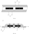
- the first line segments 201 are disposed opposite to the second line segments 202. As shown in FIG. 5 , the plurality of first line segments 201 are an upper part of the coil, and the plurality of second line segments 202 are a lower part of the coil.
- the plurality of first line segments 201 are located in the first magnetic core 10_a, and the plurality of second line segments 202 are located in the second magnetic core 10_b.
- this application does not limit a quantity of turns of the coil obtained through winding the conducting wire 20.
- the quantity of turns of the coil obtained through winding the conducting wire 20 may be designed based on an inductance required by the thin film inductor 01.
- a larger quantity of turns of the coil indicates a larger inductance of the thin film inductor 01, and a smaller quantity of turns of the coil indicates a smaller inductance of the thin film inductor 01.
- the thin film inductor 01 is applied to a power delivery circuit of a power supply.
- the film inductor 01 further includes an insulating isolation film 30.
- the insulating isolation film 30 is disposed on two sides of the conductor 20, and is located in a gap (gap) between the first magnetic film 101 and the second magnetic film 102. A lower surface and an upper surface of the insulating isolation film 30 are respectively in contact with the first magnetic film 101 and the second magnetic film 102.
- the two sides of the conductor 20 indicate two sides of the conductor 20 in a signal transmission direction (for example, the Z direction in FIG. 3 ).
- the insulating isolation film 30 separates the first magnetic film 101 from the second magnetic film 102, to prevent the first magnetic film 101 from being electrically connected to the second magnetic film 102.
- a thickness of the insulating isolation film 30 is thin.
- the thickness may be about 0.5 ⁇ m. Therefore, a magnetic line in the first magnetic film 101 can enter the second magnetic film 102 through the insulating isolation film 30, or a magnetic line in the second magnetic film 102 can enter the first magnetic film 101 through the insulating isolation film 30.
- a magnetic material with a relatively high magnetic permeability and a relatively good saturation characteristic may be used to form the first magnetic film 101 and the second magnetic film 102.
- a resistivity of the thin film inductor 01 is relatively small.
- a switch frequency of a switch transistor in a voltage conversion circuit is relatively high, relatively large loss may occur to an eddy current generated in the thin film inductor 01. In this way, the inductance of the thin film inductor 01 is reduced.
- the relatively large loss of the eddy current causes heat emitting of the thin film inductor 01, thereby reducing an inductance value Q and reducing conversion efficiency of the voltage conversion circuit.
- the first magnetic film 101 and the second magnetic film 102 each include magnetic sub-films 120 and insulating sub-films 121.
- the magnetic sub-films 120 and the insulating sub-films 121 are alternately disposed.
- the magnetic sub-films 120 and the insulating sub-films 121 are alternately disposed.
- the first magnetic film 101 and the second magnetic film 102 are in a structure of a plurality of laminated (laminated) layers of thin films.
- a direction of magnetic lines (indicated by using black arrows in the figure) of an alternating magnetic field generated by the thin film inductor 01 may be clockwise.
- a direction of magnetic lines of an alternating magnetic field generated by the thin film inductor 01 is counterclockwise.
- a closed loop current that is, the eddy current is induced in the alternating magnetic field at a section perpendicular to the direction of the magnetic lines.
- Generation of the eddy current causes additional loss, thereby weakening the magnetic field.
- a loop current is induced in the alternating magnetic field at a section perpendicular to horizontal (X direction) magnetic lines.
- the loop current is a longitudinal eddy current.
- the longitudinal eddy current formed at the section perpendicular to the X direction is separated into a plurality of sub-eddies M1 by the layers of magnetic sub-films 120 in the first magnetic film 101 and the second magnetic film 102.
- Each sub-eddy current M1 is limited to a long and narrow loop of each magnetic sub-film 120. In this way, a resistance on a path of the eddy current is increased, to reduce loss of the eddy current.
- a magnetic field generated by the eddy current is a change to an original magnetic field generated when the first magnetic film 101 and the second magnetic film 102 are powered on.
- a direction H of the original magnetic field generated when the first magnetic film 101 and the second magnetic film 102 are powered on is from inside to outside, and a direction of the eddy current is clockwise during the original magnetic field is being enhanced.
- a direction H of the original magnetic field generated when the first magnetic film 101 and the second magnetic film 102 are powered on is from inside to outside, and a direction of the eddy current is counterclockwise during the magnetic field is being weakened.
- each sub-eddy current M1 is easily limited to each layer of magnetic sub-film 120.
- the switch frequency in the circuit is a high frequency, because a capacitance effect exists between the layers of magnetic sub-films 120, that is, a higher frequency indicates a smaller impedance of a capacitor, the sub-eddy currents M1 in the magnetic sub-films 120 more easily pass through the insulating sub-films 121 and converge, to form a large eddy current path. In this way, an effect of the loss of the eddy current is reduced.
- a thickness of the insulating sub-film 121 may be appropriately increased.
- a thickness d of each layer of insulating sub-film 121 may be from 5 nm to 50 nm.
- the thickness d of the insulating sub-film 121 is less than 5 nm, and the switch frequency in the circuit is a high frequency, the impedance of the capacitor formed between the layers of magnetic sub-films 120 is relatively small, so that sub-eddy currents M1 in the magnetic sub-films 120 easily pass through the insulating sub-films 121 and converge, to reduce the effect of the loss of the eddy current.
- the thickness d of the insulating sub-film 121 is greater than 50 nm, if the first magnetic film 101 or the second magnetic film 102 is fixed, a proportion of a thickness of the magnetic sub-films 120 in a thickness of the first magnetic film 101 or the second magnetic film 102 decreases, thereby reducing an effective magnetic permeability of the thin film inductor 01.
- the thickness d of the insulating sub-film 121 may be 5 nm, 10 nm, 15 nm, 25 nm, or 50 nm.
- the insulating sub-film 121 is made of an insulating inorganic or organic material.
- a thickness t of each layer of magnetic sub-film 120 may be from 100 nm to 500 nm. When the thickness t of the magnetic sub-film 120 is less than 100 nm, the thickness t of the magnetic sub-film 120 is quite small. This does not facilitate improving the effective magnetic permeability of the thin film inductor 01.
- the thickness t of the magnetic sub-film 120 is greater than 500 nm, if the first magnetic film 101 or the second magnetic film 102 is fixed, a proportion of the thickness of the insulating sub-films 121 in the thickness of the first magnetic film 101 or the second magnetic film 102 decreases, so that the sub-eddy currents M1 in the magnetic sub-films 120 easily pass through the insulating sub-films 121 and converge, thereby reducing the effect of the loss of the eddy current.
- the thickness t of the magnetic sub-film 120 is greater than 500 nm, and the switch frequency in the circuit is a high frequency, an impedance of an eddy current path of the thin film inductor 01 decreases. This does not facilitate limiting each sub-eddy current M1 to a long and narrow loop of the magnetic sub-film 120.
- the thickness t of the magnetic sub-film 120 may be 100 nm, 150 nm, 180 nm, 250 nm, 300 nm, 350 nm, 400 nm, 450 nm, or 500 nm.
- the magnetic sub-film 120 is made of the foregoing magnetic material.
- the magnetic lines are perpendicular to a magnetic film surface of the first magnetic film 101.
- a closed loop current is induced in the alternating magnetic field at a section perpendicular to a direction (Y direction) of a vertical magnetic line.
- the loop current is a lateral eddy current M2 that is shown in FIG. 9 and that is parallel to a film surface B of the first magnetic film 101.
- a direction of the eddy current in FIG. 9 is related to the original magnetic field generated when the first magnetic film 101 and the second magnetic film 102 are powered on. Details are not described herein.
- a plane in which the lateral eddy current M2 is located is parallel to the magnetic sub-films 120 in the first magnetic film 101 or the second magnetic film 102. Therefore, the lateral eddy current M2 cannot be separated by the plurality of layers magnetic sub-films 120. In this case, loss of the eddy current at a position of the insulating isolation film 30 cannot be effectively reduced.
- the magnetic sub-films 120 and the insulating sub-films 121 in the first magnetic film 101 are exposed from a surface that is of the first magnetic film 101 and that is in contact with the insulating isolation film 30, and/or, the magnetic sub-films 120 and the insulating sub-films 121 in the second magnetic film 102 are exposed from a surface that is of the second magnetic film 102 and that is in contact with the insulating isolation film 30.
- the magnetic sub-films 120 and the insulating sub-films 121 that are exposed from the surface that is of the first magnetic film 101 and that is in contact with the insulating isolation film 30 and/or the surface that is of the second magnetic film 102 and that is in contact with the insulating isolation film 30 intersect a plane in which an eddy current generated from magnetic lines passing through the insulating isolation film 30.
- the magnetic lines passing through the insulating isolation film 30 can enter the first magnetic film 101 and/or the magnetic sub-films 120 exposed from the surface in contact with the insulating isolation film 30.
- the eddy current generated in the plane perpendicular to the magnetic lines is separated into the plurality of sub-eddy currents by the layers of magnetic sub-films 120.
- each sub-eddy current enters one layer of magnetic sub-film 120.
- each sub-eddy current can be limited to one layer of magnetic sub-film 120, to reduce loss of the eddy current.
- the magnetic core 10 can be described by using an example.
- the magnetic sub-films 120 intersect the plane in which the eddy current generated from the magnetic lines passing through the insulating isolation film 30 is located.
- the surface that is of the first magnetic film 101 and that is in contact with the insulating isolation film 30 and the surface that is of the second magnetic film 102 and that is in contact with the insulating isolation film 30 are inclined surfaces C with a same slope.
- a thickness of the insulating isolation film 30 is the same at all positions.
- the included angle ⁇ may be an acute angle shown in FIG. 11a .
- the included angle ⁇ is an obtuse angle. This is not limited in this application.
- the lower surface D of the first magnetic film 101 is a surface that is of the first magnetic film 101 and that is away from the second magnetic film 102.
- the magnetic sub-films 120 and the insulating sub-films 121 in the first magnetic film 101 are parallel to the lower surface D of the first magnetic film 101.
- a physical vapor deposition (Physical Vapor Deposition, PVD) process is applied on a bearing surface of a substrate for a plurality of times to implement alternately sputtering, to form the magnetic sub-films 120 and insulating sub-films 121 that are alternately disposed, thereby finally forming the first magnetic film 101.
- PVD Physical Vapor Deposition
- the magnetic sub-films 120 and the insulating sub-films 121 formed in the foregoing steps are parallel to the bearing surface of the substrate, so that the magnetic sub-films 120 and the insulating sub-films 121 in the first magnetic film 101 can be parallel to the lower surface D of the first magnetic film 101 (that is, the surface that is of the first magnetic film 101 and that is in contact with the bearing surface of the substrate).
- the magnetic sub-films 120 and the insulating sub-films 121 in the first magnetic film 101 intersect the inclined surface C, so that the magnetic sub-films 120 and the insulating sub-films 121 in the first magnetic film 101 can be exposed from the inclined surface C.
- the inclined surface C may be prepared by using a lift-off (lift-off) process.
- lift-off process is described in detail in the following description.
- the insulating isolation film 30 and the conductor 20 are prepared.
- the magnetic sub-films 120 and the insulating sub-films 121 in the second magnetic film 102 are parallel to the lower surface D of the first magnetic film 101.
- the inclined surface C may also be formed at the surface that is of the second magnetic film 102 and that is in contact with the insulating isolation film 30.
- the surface that is of the first magnetic film 101 and that is in contact with the insulating isolation film 30 and the surface that is of the second magnetic film 102 and that is in contact with the insulating isolation film 30 are the inclined surfaces C.
- the included angle ⁇ between the lower surface D of the first magnetic film 101 and each of the surface that is of the first magnetic film 101 and that is in contact with the insulating isolation film 30 and the surface that is of the second magnetic film 102 and that is in contact with the insulating isolation film 30 is an acute angle.
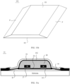
- the first magnetic film 101 shown in FIG. 11a may be a trapezoidal frustum shown in FIG. 11b .
- An upper base E1 of the trapezoidal frustum is close to the second magnetic film 102, and a lower base E2 is away from the second magnetic film 102.
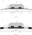
- the thin film inductor 01 further includes a flattened dielectric layer 22, a magnetic flux hole 23, and an interlayer dielectric layer 24.
- the flattened dielectric layer 22 covers the upper base of the trapezoidal frustum, that is, the first magnetic film 101, and a part of side surfaces F of the trapezoidal frustum.
- a dielectric layer may be first deposited on the substrate on which the first magnetic film 101 is prepared.
- a material of the dielectric layer may include at least one of Si 3 N 4 or SiO 2 .
- CPM Chemical Mechanical Planarization
- a part of the material of the flattened dielectric layer 22 is etched, to form the magnetic flux hole 23.
- the insulating isolation film 30 is located in the magnetic flux hole 23, and covers the other part of the side surfaces F of the trapezoidal frustum.
- the interlayer dielectric layer 24 covers an upper surface of the flattened dielectric layer 22 and a sidewall of the magnetic flux hole 23.
- the interlayer dielectric layer 24 and the insulating isolation film 30 are made of the same material.
- the material may be at least one of Si 3 N 4 or SiO 2 .
- the interlayer dielectric layer 24 and the insulating isolation film 30 may be an integrated structure.
- a dielectric layer may be deposited by using the same deposition process on the substrate on which the flattened dielectric layer 22 and the magnetic flux hole 23 are prepared.
- a part that is of the dielectric layer, that is located in the magnetic flux hole 23, and that is in contact with the side surfaces of the trapezoidal frustum, that is, the first magnetic film 101 is the insulating isolation film 30.
- the interlayer dielectric layer 24 is the interlayer dielectric layer 24.
- the flattened dielectric layer 22 and a part that is of the interlayer dielectric layer 24 and that covers the upper base E1 of the trapezoidal frustum, that is, the first magnetic film 101 serve as a lower support layer 26 for bearing the conductor 20.
- the lower support layer 26 is made of an inorganic material, for example, mainly Si 3 N 4 and/or SiO 2 .
- a tail 25 of the second magnetic film 102 covers the sidewall on a side that is of the magnetic flux hole 23 and that is away from the accommodation cavity 21, and covers, after a turning, the upper surface of the interlayer dielectric layer 24 connected to the sidewall.
- An end that is of the tail 25 of the second magnetic film 102 and that is away from the accommodation cavity 21 has a taper angle ⁇ .
- the taper angle ⁇ is from 10° to 90°.
- the taper angle ⁇ may be 12°, 15°, 19°, 20°, 30°, 60°, or 85°.
- the thin film inductor 01 further includes a seed layer (Seed layer) 27, an upper support layer 28, and an adhesion layer (Adhesion layer) 29.
- the seed layer 27 is located in the accommodation cavity 21.
- the seed layer 27 is in contact with a surface that is of the conductor 20 and that is close to the first magnetic film 101.
- a material forming the seed layer 27 includes at least one of titanium (Ti) or copper (Cu).
- the conductor 20 may be disposed on an upper surface of the lower support layer 26 by using the seed layer 27.
- the upper support layer 28 is located in the accommodation cavity 21.
- the upper support layer 28 covers surfaces of the conductor 20 except the surface in contact with the seed layer 27.
- a material forming the upper support layer 28 may be an organic macromolecular polymer (Polymer).
- the upper support layer 28 has a relatively large thickness relative to the lower support layer 26 (as shown in FIG. 11a ), to support the second magnetic film 102.
- the thickness of the upper support layer 28 is adjusted to adjust a height of the entire thin film inductor 01.
- a film length of the second magnetic film 102 covering the upper support layer 28 is greater than a film length of the first magnetic film 101 covering the substrate in the X direction (in FIG. 11a , the hard axis of the film inductor 01).
- a film length of the second magnetic film 102 and a film length of the first magnetic film 101 are not limited in the Z direction (in FIG. 3 , the easy axis of the film inductor 01).
- the film length of the second magnetic film 102 may be greater than the film length of the first magnetic film 101.
- the film length of the second magnetic film 102 may be less than the film length of the first magnetic film 101.
- the adhesion layer 29 is disposed on a surface that is of the second magnetic film 102 and that is close to the first magnetic film 101.
- a material forming the adhesion layer 29 includes at least one of tantalum (Ta), titanium (Ti), titanium nitride (TiN), or tantalum nitride (TaN).
- the adhesion layer 29 is configured to bond the second magnetic film 102 to the upper support layer 28, a magnetic film air gap film layer 30, and the interlayer dielectric layer 24.
- FIG. 11d a specific structure of the thin film inductor 01 is shown in FIG. 11d when the included angle ⁇ between the lower surface D of the first magnetic film 101 and each of the surface that is of the first magnetic film 101 and that is in contact with the insulating isolation film 30 and the surface that is of the second magnetic film 102 and that is in contact with the insulating isolation film 30 is an acute angle.
- the first magnetic film 101 is the trapezoidal frustum shown in FIG 11b .
- the upper base E1 of the trapezoidal frustum is close to the second magnetic film 102, and the lower base E2 is away from the second magnetic film 102.
- a difference between the structure shown in FIG. 11a and that shown in FIG. 11d is that the side surfaces F of the trapezoidal frustum are fully covered by the insulating isolation film 30.
- the thin film inductor 01 shown in FIG. 11d further includes the flattened dielectric layer 22 and the interlayer dielectric layer 24.
- the flattened dielectric layer 22 covers the upper base E1 of the trapezoidal frustum.
- a material of the flattened dielectric layer 22 is the same as that described above. Details are not described herein again.
- a dielectric layer may be first deposited on the substrate on which the first magnetic film 101 is prepared.
- a material of the dielectric layer may include Si 3 N 4 and/or SiO 2 .
- CPM Chemical Mechanical Planarization
- an etching process is used to remove a part of the dielectric layer except the part covering the upper base E1 of the trapezoid frustum, to obtain the flattened dielectric layer 22 shown in FIG. 11d .
- the interlayer dielectric layer 24 covers the flattened dielectric layer 22.
- the interlayer dielectric layer 24 and the insulating isolation film 30 are made of the same material and are an integrated structure.
- a dielectric layer may be deposited by using the same deposition process on the substrate on which the flattened dielectric layer 22 is prepared.
- a part that is of the dielectric layer and that covers the side surfaces of the trapezoid frustum, that is, the first magnetic film 101 serves as the insulating isolation film 30.
- the remaining part of the dielectric layer is the interlayer dielectric layer 24.
- the flattened dielectric layer 22 and the part that is of the interlayer dielectric layer 24 and that covers the upper base E1 of the trapezoidal frustum, that is, the first magnetic film 101 serve as the lower support layer 26 for bearing the conductor 20.
- the lower support layer 26 is made of an inorganic material, for example, mainly Si 3 N 4 and/or SiO 2 .
- an end that is away from the accommodation cavity 21 and that is of a part that is of the second magnetic film 102 and that is in contact with the insulating isolation film 30 has a taper angle ⁇ .
- the taper angle ⁇ is from 10° to 90°.
- the taper angle ⁇ may be 12°, 15°, 19°, 20°, 30°, 60°, or 85°.
- the thin film inductor 01 shown in FIG. 11d also has the seed layer 27, the upper support layer 28, and the adhesion layer 29. A manner of setting these thin film layers is the same as that described above. Details are not described herein again.
- the following uses the structure shown in FIG. 11a as an example to describe a process in which the inclined surfaces C can be used to reduce loss of the eddy current at the insulating isolation film 30 in the thin film inductor 01 when the surface that is of the first magnetic film 101 and that is in contact with the insulating isolation film 30 and the surface that is of the second magnetic film 102 and that is in contact with the insulating isolation film 30 are the inclined planes C.
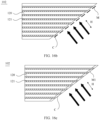
- the magnetic lines passing through the insulating isolation film 30 are perpendicular to the surface that is of the first magnetic film 101 and that is in contact with the insulating isolation film 30, that is, the inclined surface C shown in FIG. 13 .
- the eddy current M is induced in the alternating magnetic field at the section perpendicular to the direction of the magnetic lines, that is, the section parallel to the inclined surface C.
- the magnetic sub-films 120 and the insulating sub-films 121 in the first magnetic film 101 are parallel to the lower surface D of the first magnetic film 101, as shown in FIG. 10 , the magnetic sub-films 120 and the insulating sub-films 121 in the first magnetic film 101 can be exposed from the surface that is of the first magnetic film 101 and that is in contact with the insulating isolation film 30, that is, the inclined surface C shown in FIG. 13 . In this case, the magnetic lines passing through the insulating isolation film 30 can enter the magnetic sub-films 120 in the first magnetic film 101 shown in FIG. 14 .
- each sub-eddy current M1 is separated into the plurality of sub-eddy currents M1 by the layers of magnetic sub-films 120.
- each sub-eddy current M1 enters one layer of magnetic sub-film 120.
- each sub-eddy current M1 can be limited to each layer of magnetic sub-film 120, to reduce loss of the eddy current.
- the magnetic lines passing through the insulating isolation film 30 are perpendicular to the surface that is of the first magnetic film 101 and that is in contact with the insulating isolation film 30, that is, the inclined surface C shown in FIG. 13 , so that the magnetic lines can enter the magnetic sub-films 120 in the first magnetic film 101.
- This is the same as Example 1.
- the eddy current M is induced in the alternating magnetic field at the section perpendicular to the direction of the magnetic lines, that is, the section parallel to the inclined surface C.
- each sub-eddy current M1 is separated into the plurality of sub-eddy currents M1 by the layers of magnetic sub-films 120.
- each sub-eddy current M1 enters one layer of magnetic sub-film 120.
- each sub-eddy current M1 can be limited to each layer of magnetic sub-film 120, to reduce loss of the eddy current.
- the magnetic lines passing through the insulating isolation film 30 from the first magnetic film 101 are perpendicular to the surface that is of the second magnetic film 102 and that is in contact with the insulating isolation film 30, that is, the inclined surface C shown in FIG. 16b , so that the magnetic lines can enter the magnetic sub-films 120 in the second magnetic film 102 shown in FIG. 16c .
- This is the same as Example 1.
- the eddy current M is induced in the alternating magnetic field at the section perpendicular to the direction of the magnetic lines, that is, the section parallel to the inclined surface C.
- each sub-eddy current M1 is separated into the plurality of sub-eddy currents M1 by the layers of magnetic sub-films 120.
- each sub-eddy current M1 enters one layer of magnetic sub-film 120.
- each sub-eddy current M1 can be limited to each layer of magnetic sub-film 120, to reduce loss of the eddy current.
- the surface that is of the first magnetic film 101 and that is in contact with the insulating isolation film 30 and the surface that is of the second magnetic film 102 and that is in contact with the insulating isolation film 30 are curved surfaces S with same curvature.
- a thickness of the insulating isolation film 30 is the same at all positions.
- the magnetic sub-films 120 and the insulating sub-films 121 in the first magnetic film 101 and the second magnetic film 102 are parallel to the lower surface D of the first magnetic film 101.
- the magnetic sub-films 120 and the insulating sub-films 121 in the first magnetic film 101 are exposed from the curved surface S that is of the first magnetic film 101 and that is in contact with the insulating isolation film 30.
- the magnetic lines passing through the insulating isolation film 30 enter the magnetic sub-films 120 in the first magnetic film 101.
- the sub-eddy current M1 is induced in the alternating magnetic field at a section perpendicular to a direction of a magnetic line.
- the sub-eddy currents M1 can be respectively limited to the magnetic sub-films 120, to reduce loss of the eddy current.
- the thickness of the insulating isolation film 30 does not need to be the same at all positions, in the magnetic core 10, only the surface that is of the second magnetic film 102 and that is in contact with the insulating isolation film 30 may be set to the curved surface S.
- the surface that is of the first magnetic film 101 and that is in contact with the insulating isolation film 30 is set to the curved surface S.
- a process of reducing loss of the eddy current at the position of the insulating isolation film 30 by using the surface S may be obtained in the same manner. Details are not described herein again.
- the thin film inductor 01 shown in FIG. 17 also has the flattened dielectric layer 22, the interlayer dielectric layer 24, the seed layer 27, the upper support layer 28, and the adhesion layer 29.
- a manner of setting these thin films is the same as that described above. Details are not described herein again.
- the thin film inductor 01 further includes a support pad 40.
- the support pad 40 is located below the first magnetic film 101, and corresponds to the position of the insulating isolation film 30.
- a material forming the support pad 40 may be a non-magnetic material.
- first magnetic film 101 a part below the first magnetic film 101 is a side that is of the first magnetic film 101 and that is away from the second magnetic film 102.
- an upper surface G of the support pad 40 is in contact with the insulating isolation film 30.
- the first magnetic film 101 covers two sides of the upper surface G of the support pad 40. In the first magnetic film 101 covering the support pad 40, the magnetic sub-films 120 and the insulating sub-films 121 are in contact with the insulating isolation film 30.
- the surface that is of the support pad 40 and that is in contact with the first magnetic film 101 is a curved surface.
- the magnetic sub-films 120 and the insulating sub-films 121 in the first magnetic film 101 alternately cover the curved surface of the support pad 40.
- the magnetic sub-films 120 and the insulating sub-films 121 in the first magnetic film 101 are also in a curved state.
- a curvature of these sub-films is the same as or similar to a curvature of the curved surface of the support pad 40 covered by these sub-films.
- the magnetic sub-films 120 and the insulating sub-films 121 in the first magnetic film 101 are in the curved state. Therefore, in the first magnetic film 101, the magnetic sub-films 120 and the insulating sub-films 121 that cover the support pad 40 intersect a plane in which the insulating isolation film 30 is located. In this way, the magnetic sub-films 120 and the insulating sub-films 121 in the first magnetic film 101 can be exposed from the surface that is of the first magnetic film 101 and that is in contact with the insulating isolation film 30.
- the surface that is of the support pad 40 and that is in contact with the first magnetic film 101 is an arc surface.
- a lower surface of the support pad 40 is flush with the lower surface of the first magnetic film 101.
- FIG. 7b a partial structure of the thin film inductor 01 at the position of the left-side insulating isolation film 30 is used as an example.
- a plurality of magnetic lines of the alternating magnetic field at the position of the insulating isolation film 30 pass through the insulating isolation film 30 from the second magnetic film 102, then separately enter the curved magnetic sub-films 120 in the first magnetic film 101 covering the support pad 40, and then go along a direction of laying the magnetic sub-films 120.
- the plurality of magnetic lines passing through the insulating isolation film 30 can enter the layers of magnetic sub-films 120 in the first magnetic film 101. Therefore, the sub-eddy currents M1 are induced in the alternating magnetic field at sections perpendicular to the magnetic lines. As shown in FIG. 8 , the sub-eddy current M1 is limited to the layers of magnetic sub-films 120, thereby reducing loss of the eddy current.
- the thin film inductor 01 shown in FIG. 19 also has the flattened dielectric layer 22, the interlayer dielectric layer 24, the seed layer 27, the upper support layer 28, and the adhesion layer 29.
- a manner of setting these thin films is the same as that described above. Details are not described herein again.
- the integrated circuit 02 includes a silicon substrate 50 and any foregoing described thin film inductor 01 disposed on the silicon substrate 50.
- the integrated circuit 02 has technical effects the same as the thin film inductor 01 provided in the foregoing embodiment. Details are not described herein again.
- the material forming the silicon substrate 50 includes Si and a polymer (polymer).
- the integrated circuit 02 may be a System-on-Chip (SoC), a central processing unit (central processing unit, CPU), a graphics processing unit (graphics processing unit, GPU), or a power management integrated circuit (power management integrate circuit, PMIC).
- SoC System-on-Chip
- CPU central processing unit
- GPU graphics processing unit
- PMIC power management integrated circuit
- the integrated circuit 02 further includes a circuit structure 51 disposed on the silicon substrate 50, a circuit-inductor interconnection layer 52 sequentially covering the circuit structure 51, and a chip encapsulation structure 53.
- the circuit structure 51 includes a plurality of transistors 501, and a metal interconnection layer 502 configured to connect the plurality of transistors 501 together to form a circuit.
- the transistor 501 may be a transistor prepared by using a complementary metal oxide semiconductor (complementary metal oxide semiconductor, CMOS) process, a silicon germanium (SiGe) process, or a gallium nitride (GaN) process.
- CMOS complementary metal oxide semiconductor
- SiGe silicon germanium
- GaN gallium nitride
- the metal interconnection layer 502 includes a plurality of dielectric layers or passivation layers (passivation layer), and a metal conducting wire embedded in the dielectric layers or the passivation layers.
- a material forming the dielectric layer or the passivation layer in the metal interconnection layer 502 includes any one of silicon dioxide (SiO 2 ), silicon nitride (Si 3 N 4 ), and polyimide (polyimide).
- the thin film inductor 01 is located between the circuit-inductor interconnection layer 52 and the chip encapsulation structure 53.
- the circuit-inductor interconnection layer 52 is configured to electrically connect the thin film inductor 01 to the circuit structure 51 located below the thin film inductor 01.
- the manner of setting the thin film inductor 01 in the integrated circuit 02 may be that the first magnetic film 101 is closer to the silicon substrate 50 (the left-side thin film inductor 01) than the second magnetic film 102; or the second magnetic film 102 in the thin film inductor 01 is closer to the silicon substrate 50 (the right-side thin film inductor 01) than the first magnetic film 101.
- a package assembly structure configured to implement signal interconnection between a circuit and an inductor, for example, an interconnection path (Via), a solder pillar (solder pillar), a copper pillar (copper pillar), a micro bump (micro bump), or a lead bump (solder bump) is disposed in the circuit-inductor interconnection layer 52.
- the chip encapsulation structure 53 may be prepared by using a wafer-level packaging (wafer-level packaging, WLP) process.
- WLP wafer-level packaging
- the chip encapsulation structure includes an encapsulation substrate and encapsulation cabling disposed inside the encapsulation substrate.
- a chip encapsulation pin 54 is disposed above the chip encapsulation structure 53, so that the entire integrated circuit 02 can be connected to a printed circuit board (printed circuit board, PCB).
- the terminal device includes at least one integrated circuit 02 described above.
- the mobile terminal 03 further includes a power management chip 60 and a power bus or a power delivery network of a power supply that is connected to the power management chip 60.
- the power management chip 60 includes the integrated circuit 02, and the thin film inductor 01 is integrated into the integrated circuit 02.
- the power management chip 60 may provide working voltage to other components of the terminal device 03 by using the power bus, for example, a radio frequency transceiver (radio frequency module), a memory, a hard disk, a camera and an image processor (imaging processing module), an input/output (I/O) interface, and a man-machine interaction device.
- the mobile terminal 03 further includes a processor 61 and a data bus (Data bus) connected to the processor 61.
- the processor 61 includes the integrated circuit 02.
- the integrated circuit 02 is an integrated power module
- the thin film inductor 01 is integrated into the integrated power module.
- the processor 61 may provide working voltage to other components of the terminal device 03 by using the power bus, for example, the radio frequency transceiver, the memory, the hard disk, the camera and the image processor, the input/output interface, and the man-machine interaction device.
- the power bus for example, the radio frequency transceiver, the memory, the hard disk, the camera and the image processor, the input/output interface, and the man-machine interaction device.
- the processor 61 may be any one of a SoC, a CPU, and a GPU.
- terminal device 03 has technical effects the same as the integrated circuit 02 provided in the foregoing embodiment. Details are not described herein again.
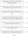
- An embodiment of this application provides a method for preparing the thin film inductor 01 shown in FIG. 11a . As shown in FIG. 23 , the method includes steps S101 to S105.
- the first magnetic film 101 is a trapezoid frustum.
- An upper base E1 of the trapezoidal frustum is away from the substrate, and a lower base E2 is close to the substrate.
- magnetic sub-films 120 and insulating sub-films 121 in the first magnetic film 101 are exposed from side surfaces F of the trapezoid frustum.
- composition process in this embodiment of this application includes a photolithography process, or includes a photolithography process and an etching step, or includes printing, ink jetting, another process for forming a predetermined pattern, or the like.
- the photolithography process indicates a process that includes processes of film forming, exposing, developing, and the like and in which a photoresist, a mask reticle, an exposure machine, and the like are used to form a pattern.
- a preparing process of preparing the first magnetic film 101 by using the lift-off process is as follows:
- a photoresist 70 coats the substrate.
- the photoresist 70 in this embodiment of this application may be a positive photoresist, or may be a negative photoresist. This is not limited in the present invention.
- a mask reticle 71 is configured to implement mask exposure on the photoresist 70.
- a developing process is performed on the photoresist after the exposure performed by using the mask reticle.
- the photoresist shielded by the mask reticle 71 is not irradiated by light, and therefore is dissolved in a developing solution.
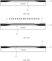
- an adhesion layer (a black film layer in FIG. 24d ) is deposited on the substrate on which the foregoing structures are formed.
- a physical vapor deposition process is used for a plurality of times to implement alternately sputtering, to form magnetic sub-films 120 and insulating sub-films 121 that are alternately disposed.
- the photoresist 70 is lifted off, thereby forming the first magnetic film 101 in a trapezoidal frustum shape on the substrate.
- a first dielectric layer 80 is deposited.
- a CPM process is performed on the first dielectric layer 80, so that an upper surface of the first dielectric layer 80 is flat to some extent as shown in FIG. 25b .
- the first dielectric layer 80 is exposed by using the mask reticle 71 and the photoresist 70.
- the developing process is performed on the photoresist 70.
- a part that is of the photoresist 70 and that is irradiated by light is dissolved in the developing solution.
- a dry etching process is used to etch a part that is the first dielectric layer 80 and that is not covered by the photoresist 70, to form a magnetic flux hole 23 shown in FIG. 25e .
- a part of a side surface F of the first magnetic film 101 in the trapezoidal frustum shape is exposed at a bottom of the magnetic flux hole 23.
- a size of an opening of the magnetic flux hole 23 is controlled, so that the first dielectric layer 80 can cover a part of the side surface of the trapezoid frustum.
- the part of the side surface F of the first magnetic film 101 in the trapezoidal frustum shape is exposed in the magnetic flux hole 23, and the other part is covered by the first dielectric layer 80.
- the first dielectric layer 80 further covers the upper base of the trapezoidal frustum.
- the first dielectric layer 80 formed by using the composition process may serve as the flattened dielectric layer 22.
- a second dielectric layer 81 is deposited.
- the second dielectric layer 81 covers an upper surface of the first dielectric layer 80 and a side wall of the magnetic flux hole 23, and is in contact with the other part of the side surface of the trapezoidal frustum by using the magnetic flux hole 23.
- a part that is of the second dielectric layer 81 and that is in contact with the side surface of the trapezoidal frustum serves as the insulating isolation film 30.
- the photoresist 70 above the upper base E1 of the trapezoidal frustum, that is, the first magnetic film 101 is formed by using the composition process, and the photoresist is exposed by using the mask reticle 71.
- the developing process is used and performed on the photoresist 70 after the exposure, so that the photoresist 70 irradiated by light is removed through the developing process.
- a material forming the conductor 20 may be at least one of copper (Cu), titanium (Ti), nickel (Ni), or gold (Au).
- An accommodation cavity 21 for accommodating the conductor 20 is formed between the first magnetic film 101 and the second magnetic film 102.
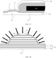
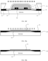
- the photoresist 70 coats the structure of FIG. 27d . Because the photoresist 70 is used to form an upper support layer 28, the photoresist 70 has a relatively large thickness. Then, the photoresist 70 is exposed by using the mask reticle 71.
- the developing process is performed on the photoresist 70 after the exposure, and a thermal reflow (thermal reflow) process is performed on the photoresist 70 after the developing process, to form the upper support layer 28 shown in FIG. 28c .
- the photoresist 70 coats the structure shown in FIG. 28c , and the photoresist 70 is exposed by using the mask reticle 71.
- the developing process is performed on the photoresist 70 after the exposure.
- the physical vapor deposition process is used for a plurality of times to implement alternately sputtering, to form magnetic sub-films 120 and insulating sub-films 121 that are alternately disposed.
- a tail of the prepared second magnetic film 102 covers a sidewall on a side that is of the magnetic flux hole 23 and that is away from the accommodation cavity 21, and covers, after a turning, an upper surface of the interlayer dielectric layer 24 connected to the sidewall.
- an end that is of the tail 25 of the second magnetic film 102 and that is away from the accommodation cavity 21 has a taper angle ⁇ .
- the taper angle ⁇ is less than 90°.
- the method for preparing the thin film inductor 01 has technical effects the same as the magnetic film inductor 01 provided in the foregoing embodiment. Details are not described herein again.
- An embodiment of this application provides a method for preparing the thin film inductor 02 shown in FIG. 11d .
- the method still includes the foregoing steps S101 to S105.
- a structure of the thin film inductor 02 is different from the structure shown in FIG. 11a . Therefore, specific processes of some steps in the foregoing steps S101 to S105 are also different. The following describes in detail the specific processes of these steps.
- step S101 is performed.
- a process of preparing the first magnetic film 101 is the same as the foregoing description. Details are not described herein again.
- step S102 In a process of performing step S102, first, steps in FIG. 25a and FIG. 25b are performed.
- the first dielectric layer 80 is deposited on the substrate on which the first magnetic film 101 is formed.
- a flattening process is performed on the first dielectric layer 80.
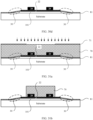
- the photoresist 70 coats the substrate on which the foregoing structures are formed, and the photoresist 70 is exposed by using the mask reticle 71. Then, as shown in FIG. 29b , the developing process is performed on the photoresist 70 after the exposure.
- the first dielectric layer 80 that is not covered by the photoresist 70 is etched to form the flattened dielectric layer 22.
- the first dielectric layer 80 formed by using the composition process, that is, the flattened dielectric layer 22 covers the upper base E1 of the trapezoid frustum.
- the photoresist on a surface of the flattened dielectric layer 22 is removed.
- the second dielectric layer 81 is deposited on the substrate on which the foregoing structures are formed.
- the second dielectric layer 81 covers the flattened dielectric layer 22.
- a part that is of the second dielectric layer 81 and that fully covers the side surfaces of the trapezoid frustum, that is, the first magnetic film 101 serves as the insulating isolation film 30.
- the photoresist 70 coats the substrate on which the insulating isolation film 30 is formed, and the photoresist 70 is exposed by using the mask reticle 71.
- the developing process is performed on the photoresist 70 after the exposure, to remove a part of the photoresist 70.
- the conductor 20 located above the upper base E1 of the trapezoidal frustum is formed by using the composition process.
- the photoresist 70 on a surface of the conductor 20 is lifted off.
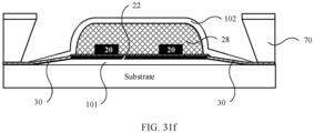
- the photoresist 70 coats the structure of FIG. 30d . Because the photoresist 70 is used to form the upper support layer 28, the photoresist 70 has a relatively large thickness. Next, the photoresist 70 is exposed by using the mask reticle 71.
- the developing process is performed on the photoresist 70 after the exposure, and a thermal reflow process is performed on the photoresist 70 after the developing process, to form the upper support layer 28 shown in FIG. 31c .
- the photoresist 70 coats the structure shown in FIG. 31c , and the photoresist 70 is exposed by using the mask reticle 71.
- the developing process is performed on the photoresist 70 after the exposure.
- the physical vapor deposition process is used for a plurality of times to implement alternately sputtering, to form the magnetic sub-films 120 and the insulating sub-films 121 that are laminated and alternately disposed.
- the tail of the prepared second magnetic film 102 flatly covers the upper surface of the insulating isolation film 30.
- an end that is of the tail 25 of the second magnetic film 102 and that is away from the accommodation cavity 21 has a taper angle ⁇ .
- the taper angle ⁇ is less than 90°.
- the method for preparing the thin film inductor 01 has technical effects the same as the magnetic film inductor 01 provided in the foregoing embodiment. Details are not described herein again.
- This application provides a method for preparing a thin film inductor 01. As shown in FIG. 32 , the method includes steps S201 to S207.
- FIG. 33a As shown in FIG. 33a , two spaced support pads 40 are disposed on a substrate 02. A surface that is of the support pad 40 and that is away from the substrate 02 is a curved surface.
- a material forming the support pad 40 may be a non-magnetic material.
- the substrate 02 may be a silicon substrate.
- a surface that is of the support pad 40 and that is away from the substrate 02 is an arc surface.
- a first magnetic film 101 is formed by using a composition process on the substrate 02 on which the support pads 40 are formed.
- the first magnetic film 101 includes magnetic sub-films 121 and insulating sub-films 120 that are alternately disposed.
- a method for preparing the first magnetic film 101 is the same as the method described above. Details are not described herein again.
- a composition process is performed on a dielectric layer at the positions of the support pads 40, for example, a dielectric layer with the same material as the second dielectric layer 81, to form an insulating isolation film 30.
- the formed insulating isolation film 30 covers the upper surfaces of the support pads 40, and sides of magnetic sub-films 120 and the insulating sub-films 121 in the first magnetic film 101 on two sides of the upper surfaces of the support pads 40.
- a part of the second dielectric layer 81 except the insulating isolation film 30 may be used as a lower support layer 26.
- a conductor 20 on the lower support layer 26 is formed on the substrate 02 on which the foregoing structures are formed.
- a process for preparing the conductor 20 is the same as the process described above. Details are not described herein again.
- an upper support layer 28 is formed on the substrate 02 on which the foregoing structures are formed.
- a process for preparing the upper support layer 28 is the same as the process described above. Details are not described herein again.
- a second magnetic film 102 is formed by using a composition process on the substrate 02 on which the foregoing structures are formed.
- the second magnetic film 102 includes magnetic sub-films 120 and insulating sub-films 121 that are alternately disposed.
- a method for preparing the second magnetic film 102 is the same as the method described above. Details are not described herein again.
- the method for preparing the thin film inductor 01 has technical effects the same as the thin film inductor 01 provided in the foregoing embodiment. Details are not described herein again.
Landscapes
- Engineering & Computer Science (AREA)
- Power Engineering (AREA)
- Microelectronics & Electronic Packaging (AREA)
- Manufacturing & Machinery (AREA)
- Coils Or Transformers For Communication (AREA)
- Semiconductor Integrated Circuits (AREA)
Claims (18)
- Dünnfilminduktor, umfassend:einen magnetischen Kern (10), wobei der magnetische Kern (10) einen ersten magnetischen Film (101) und einen zweiten magnetischen Film (102) umfasst, und ein Aufnahmehohlraum (21) zwischen dem ersten magnetischen Film (101) und dem zweiten magnetischen Film (102) vorhanden ist;einen Leiter (20), der sich in dem Aufnahmehohlraum (21) befindet; undeinen isolierenden Isolierfilm (30), der auf zwei Seiten des Leiters (20) angeordnet ist und sich zwischen dem ersten magnetischen Film (101) und dem zweiten magnetischen Film (102) befindet, wobei der isolierende Isolierfilm (30) in Kontakt mit dem ersten magnetischen Film (101) und dem zweiten magnetischen Film (102) ist; wobei der erste magnetische Film (101) und der zweite magnetische Film (102) jeweils magnetische Subfilme (120) und isolierende Subfilme (121) umfassen;in dem ersten magnetischen Film (101) die magnetischen Subfilme (120) und die isolierenden Subfilme (121) alternierend angeordnet sind;in dem zweiten magnetischen Film (102) die magnetischen Subfilme (120) und die isolierenden Subfilme (121) alternierend angeordnet sind;dadurch gekennzeichnet, dassdie magnetischen Subfilme (120) und die isolierenden Subfilme (121) in dem ersten magnetischen Film (101) von einer Oberfläche exponiert sind, die von dem ersten magnetischen Film (101) ist und die in Kontakt mit dem isolierenden Isolierfilm (30) ist; und/oder die magnetischen Subfilme (120) und die isolierenden Subfilme (121) in dem zweiten magnetischen Film (102) von einer Oberfläche exponiert sind, die von dem zweiten magnetischen Film (102) ist und die in Kontakt mit dem isolierenden Isolierfilm (30) ist.
- Dünnfilminduktor nach Anspruch 1, wobeidie Oberfläche, die von dem ersten magnetischen Film (101) ist und die in Kontakt mit dem isolierenden Isolierfilm (30) ist, und/oder die Oberfläche, die von dem zweiten magnetischen Film (102) ist und die in Kontakt mit dem isolierenden Isolierfilm (30) ist, eine geneigte Oberfläche ist;die magnetischen Subfilme (120) und die isolierenden Subfilme (121) in dem ersten magnetischen Film (101) und dem zweiten magnetischen Film (102) parallel zu der unteren Oberfläche des ersten magnetischen Films (101) sind; unddie untere Oberfläche des ersten magnetischen Films (101) eine Oberfläche ist, die von dem ersten magnetischen Film (101) ist und die von dem zweiten magnetischen Film (102) entfernt liegt.
- Dünnfilminduktor nach Anspruch 1, wobei
die Oberfläche, die von dem ersten magnetischen Film (101) ist und die in Kontakt mit dem isolierenden Isolierfilm (30) ist, und die Oberfläche, die von dem zweiten magnetischen Film (102) ist und die in Kontakt mit dem isolierenden Isolierfilm (30) ist, geneigte Oberflächen mit derselben Neigung sind. - Dünnfilminduktor nach Anspruch 2 oder 3, wobei der erste magnetische Film (101) ein trapezförmiger Stumpf ist, eine obere Basis des trapezförmigen Stumpfes nahe an dem zweiten magnetischen Film (102) liegt, und eine untere Basis von dem zweiten magnetischen Film (102) entfernt liegt; und
der Dünnfilminduktor des Weiteren umfasst:eine abgeflachte Dielektrikumschicht (22), die die obere Basis des trapezförmigen Stumpfes und einen Teil der Seitenoberflächen des trapezförmigen Stumpfes bedeckt;ein Magnetflussloch (23), das auf der abgeflachten Dielektrikumschicht (22) hergestellt worden ist, wobei der isolierende Isolierfilm (30) sich in dem Magnetflussloch (23) befindet und den anderen Teil der Seitenoberflächen des trapezförmigen Stumpfes bedeckt; undeine Zwischenschicht-Dielektrikumschicht (24), die eine obere Basis der abgeflachten Dielektrikumschicht (22) und eine Seitenwand des Magnetflusslochs (23) bedeckt, wobei die Zwischenschicht-Dielektrikumschicht und der isolierende Isolierfilm (30) aus dem gleichen Material gefertigt sind und eine integrierte Struktur sind. - Dünnfilminduktor nach Anspruch 4, wobeiein Ausläufer (25) des zweiten magnetischen Films (102) die Seitenwand auf einer Seite, die von dem Magnetflussloch (23) ist und die von dem Aufnahmehohlraum (21) entfernt liegt, und eine obere Oberfläche bedeckt, die von der Zwischenschicht-Dielektrikumschicht ist und die mit der Seitenwand verbunden ist; undein Ende, das von dem Ausläufer (25) des zweiten magnetischen Films (102) ist und das von dem Aufnahmehohlraum (21) entfernt liegt, einen Schrägwinkel aufweist, und der Schrägwinkel 10° bis 90° beträgt.
- Dünnfilminduktor nach Anspruch 2 oder 3, wobei der erste magnetische Film (101) ein trapezförmiger Stumpf ist, eine obere Basis des trapezförmigen Stumpfes nahe an dem zweiten magnetischen Film (102) liegt, eine untere Basis von dem zweiten magnetischen Film (102) entfernt liegt, und Seitenoberflächen des trapezförmigen Stumpfes vollständig von dem isolierenden Isolierfilm (30) bedeckt sind; und
der Dünnfilminduktor des Weiteren umfasst:eine abgeflachte Dielektrikumschicht (22), die die obere Basis des trapezförmigen Stumpfes bedeckt; undeine Zwischenschicht-Dielektrikumschicht (24), die die abgeflachte Dielektrikumschicht (22) bedeckt, wobei die Zwischenschicht-Dielektrikumschicht und der isolierende Isolierfilm (30) aus dem gleichen Material gefertigt sind und eine integrierte Struktur sind. - Dünnfilminduktor nach Anspruch 6, wobei ein Ende, das von dem Aufnahmehohlraum (21) entfernt liegt und das von einem Teil ist, das von dem zweiten magnetischen Film (102) ist und das in Kontakt mit dem isolierenden Isolierfilm (30) ist, einen Schrägwinkel aufweist, wobei der Schrägwinkel 10° bis 90° beträgt.
- Dünnfilminduktor nach Anspruch 1, wobei die Oberfläche, die von dem ersten magnetischen Film (101) ist und die in Kontakt mit dem isolierenden Isolierfilm (30) ist, und/oder die Oberfläche, die von dem zweiten magnetischen Film (102) ist und die in Kontakt mit dem isolierenden Isolierfilm (30) ist, eine gekrümmte Oberfläche/gekrümmte Oberflächen ist/sind;die magnetischen Subfilme (120) und die isolierenden Subfilme (121) in dem ersten magnetischen Film (101) und dem zweiten magnetischen Film (102) parallel zu der unteren Oberfläche des ersten magnetischen Films (101) sind; unddie untere Oberfläche des ersten magnetischen Films (101) eine Oberfläche ist, die von dem ersten magnetischen Film (101) ist und die von dem zweiten magnetischen Film (102) entfernt liegt.
- Dünnfilminduktor nach Anspruch 1, wobeider Dünnfilminduktor des Weiteren ein Trägerpad (40) umfasst, wobei das Trägerpad (40) sich unter dem ersten magnetischen Film (101) befindet, und ein Teil unter dem ersten magnetischen Film (101) eine Seite ist, die von dem ersten magnetischen Film (101) ist und die von dem zweiten magnetischen Film (102) entfernt liegt;eine obere Oberfläche des Trägerpads (40) in Kontakt mit dem isolierenden Isolierfilm (30) ist;der erste magnetische Film (101) zwei Seiten der oberen Oberfläche des Trägerpads (40) bedeckt;in dem ersten magnetischen Film (101), der das Trägerpad (40) bedeckt, die magnetischen Subfilme (120) und die isolierenden Subfilme (121) in Kontakt mit dem isolierenden Isolierfilm (30) sind; undeine Oberfläche, die von dem Trägerpad (40) ist und die in Kontakt mit dem ersten magnetischen Film (101) ist, eine gekrümmte Oberfläche ist.
- Dünnfilminduktor nach Anspruch 9, wobeidie Oberfläche, die von dem Trägerpad (40) ist und die in Kontakt mit dem ersten magnetischen Film (101) ist, eine Bogenoberfläche ist; undeine untere Oberfläche des Trägerpads (40) bündig mit einer unteren Oberfläche des ersten magnetischen Films (101) ist.
- Dünnfilminduktor nach einem der Ansprüche 1 bis 10, wobei der Dünnfilminduktor des Weiteren umfasst:eine Impfschicht (27), die sich in dem Aufnahmehohlraum (21) befindet, wobei die Impfschicht (27) in Kontakt mit einer Oberfläche ist, die von dem Leiter (20) ist und die nahe an dem ersten magnetischen Film (101) liegt;eine obere Trägerschicht (28), die sich in dem Aufnahmehohlraum (21) befindet, wobei eine Oberfläche des Leiters (20), mit Ausnahme der Oberfläche in Kontakt mit der Impfschicht (27), mit der oberen Trägerschicht (28) bedeckt ist; undeine Adhäsionsschicht (29), die auf einer Oberfläche angeordnet ist, die von dem zweiten magnetischen Film (102) ist und die nahe an dem ersten magnetischen Film (101) liegt.
- Dünnschichtinduktor nach einem der Ansprüche 1 bis 11, wobei der erste magnetische Film (101) und der zweite magnetische Film (102) anisotrop sind; und
eine Länge des ersten magnetischen Films (101) kleiner als eine Länge des zweiten magnetischen Films (102) in einer Richtung einer harten Achse des Dünnfilminduktors ist. - Dünnfilminduktor nach einem der Ansprüche 1 bis 12, wobei der Leiter (20) mindestens ein Metallleiterdraht ist, der Dünnfilminduktor mindestens zwei magnetische Kerne (10) umfasst, und zwei benachbarte magnetische Kerne (10) entlang einer Längsrichtung des Metallleiterdrahts beabstandet sind.
- Dünnfilminduktor nach einem der Ansprüche 1 bis 12, wobei der Leiter (20) eine Wendel ist und der Dünnfilminduktor einen ersten magnetischen Kern (10) und einen zweiten magnetischen Kern umfasst;die Wendel eine Vielzahl von ersten Liniensegmenten (201) und eine Vielzahl von zweiten Liniensegmenten (202) umfasst, und die ersten Liniensegmente (201) gegenüber von den zweiten Liniensegmenten (202) angeordnet sind; unddie Vielzahl der ersten Liniensegmente (201) sich in dem ersten magnetischen Kern (10) befindet, und die Vielzahl der zweiten Liniensegmente (202) sich in dem zweiten magnetischen Kern befindet.
- Integrierte Schaltung, umfassend ein Siliciumsubstrat (50) und einen Dünnfilminduktor gemäß einem der Ansprüche 1 bis 14, der auf dem Siliciumsubstrat (50) angeordnet ist.
- Integrierte Schaltung nach Anspruch 15, wobei die integrierte Schaltung des Weiteren eine Schaltungsstruktur (51), die auf dem Siliciumsubstrat (50) angeordnet ist, eine Schaltung-Induktor-Interkonnektionsschicht (52), die sequentiell die Schaltungsstruktur (51) bedeckt, und eine Chipverkapselungsstruktur (53) umfasst;der Dünnfilminduktor sich zwischen der Schaltung-Induktor-Interkonnektionsschicht (52) und der Chipverkapselungsstruktur (53) befindet, und die Schaltung-Induktor-Interkonnektionsschicht (52) ausgestaltet ist, um den Dünnfilminduktor mit der Schaltungsstruktur (51) zu verbinden; undein erster magnetischer Film (101) in dem Dünnfilminduktor näher an dem Siliciumsubstrat (50) als ein zweiter magnetischer Film (102) liegt; oderder zweite magnetische Film (102) in dem Dünnfilminduktor näher an dem Siliciumsubstrat (50) liegt als ein erster magnetischer Film (101).
- Endgerät (3), umfassend mindestens eine integrierte Schaltung gemäß Anspruch 15 oder 16, wobeidas Endgerät (3) des Weiteren einen Powermanagement-Chip (60) und einen mit dem Powermanagement-Chip (60) verbundenen Powerbus umfasst, wobei der Powermanagement-Chip (60) eine integrierte Schaltung umfasst; und/oderdas Endgerät des Weiteren einen Prozessor (61) und einen mit dem Prozessor (61) verbundenen Datenbus umfasst, wobei der Prozessor (61) die integrierte Schaltung umfasst.
- Verfahren zur Herstellung des Dünnfilminduktors gemäß Anspruch 4, wobei das Verfahren umfasst:Bilden des ersten magnetischen Films (101) auf einem Substrat durch Verwenden eines Kompositionsprozesses, wobei der erste magnetische Film (101) ein trapezförmiger Stumpf ist, eine obere Basis des trapezförmigen Stumpfes von dem Substrat entfernt liegt, und eine untere Basis nahe an dem Substrat liegt; und die isolierenden Subfilme (121) in dem ersten magnetischen Film (101) von Seitenoberflächen des trapezförmigen Stumpfes exponiert sind;Abscheiden einer ersten Dielektrikumschicht (80) auf dem Substrat, auf dem der erste magnetische Film (101) gebildet ist, Durchführen eines Abflachungsprozesses auf der ersten Dielektrikumschicht (80), und Herstellen eines Magnetflusslochs (23) auf der ersten Dielektrikumschicht (80) unter Verwendung des Kompositionsprozesses, wobei die erste Dielektrikumschicht (80), die unter Verwendung des Kompositionsprozesses gebildet ist, die obere Basis des trapezförmigen Stumpfes und einen Teil der Seitenoberflächen des trapezförmigen Stumpfes bedeckt;Abscheiden einer zweiten Dielektrikumschicht (81) auf dem Substrat, auf dem die vorhergehenden Strukturen gebildet sind, wobei die zweite Dielektrikumschicht (81) eine obere Oberfläche der ersten Dielektrikumschicht (80) und eine Seitenwand des Magnetflusslochs (23) bedeckt und unter Verwendung des Magnetflussloches (23) in Kontakt mit dem anderen Teil der Seitenoberflächen des trapezförmigen Stumpfes ist; und ein Teil, der von der zweiten Dielektrikumschicht (81) ist und der in Kontakt mit den Seitenoberflächen des trapezförmigen Stumpfes ist, als isolierender Isolierfilm (30) dient;Bilden des Leiters (20) oberhalb der oberen Basis des trapezförmigen Stumpfes auf dem Substrat, auf dem der isolierende Isolierfilm (30) gebildet ist, unter Verwendung des Kompositionsprozesses, undBilden des zweiten magnetischen Films (102) auf dem Substrat, auf dem der Leiter (20) gebildet ist, unter Verwendung des Kompositionsprozesses, wobei der Aufnahmehohlraum (21) zum Aufnehmen des Leiters (20) zwischen dem ersten magnetischen Film (101) und dem zweiten magnetischen Film (102) gebildet ist.
Applications Claiming Priority (1)
| Application Number | Priority Date | Filing Date | Title |
|---|---|---|---|
| PCT/CN2018/121623 WO2020124341A1 (zh) | 2018-12-17 | 2018-12-17 | 薄膜电感及其制作方法、集成电路、终端设备 |
Publications (3)
| Publication Number | Publication Date |
|---|---|
| EP3886126A1 EP3886126A1 (de) | 2021-09-29 |
| EP3886126A4 EP3886126A4 (de) | 2021-12-22 |
| EP3886126B1 true EP3886126B1 (de) | 2024-11-27 |
Family
ID=71100041
Family Applications (1)
| Application Number | Title | Priority Date | Filing Date |
|---|---|---|---|
| EP18943437.6A Active EP3886126B1 (de) | 2018-12-17 | 2018-12-17 | Dünnschichtspule und herstellungsverfahren dafür, integrierte schaltung und endgerät |
Country Status (3)
| Country | Link |
|---|---|
| EP (1) | EP3886126B1 (de) |
| CN (2) | CN113016043B (de) |
| WO (1) | WO2020124341A1 (de) |
Families Citing this family (4)
| Publication number | Priority date | Publication date | Assignee | Title |
|---|---|---|---|---|
| CN115803832B (zh) * | 2020-07-27 | 2026-01-09 | 华为技术有限公司 | 电感器件及电子设备 |
| CN114340143B (zh) * | 2021-12-30 | 2024-06-18 | Oppo广东移动通信有限公司 | 电路板集成电感、其制备方法及电子设备 |
| US12476228B2 (en) | 2022-08-25 | 2025-11-18 | Qualcomm Incorporated | Wafer level packaging process for thin film inductors |
| WO2024044438A1 (en) * | 2022-08-25 | 2024-02-29 | Qualcomm Incorporated | Wafer level packaging process for thin film inductors |
Family Cites Families (16)
| Publication number | Priority date | Publication date | Assignee | Title |
|---|---|---|---|---|
| JP4047252B2 (ja) * | 2003-06-09 | 2008-02-13 | アルプス電気株式会社 | 薄膜構造体の製造方法 |
| JP2005109246A (ja) * | 2003-09-30 | 2005-04-21 | Tdk Corp | 高周波用磁性薄膜、その作製方法及び磁気素子 |
| JP4716308B2 (ja) * | 2005-01-12 | 2011-07-06 | Fdk株式会社 | 積層インダクタ |
| JP2008277339A (ja) * | 2007-04-25 | 2008-11-13 | Tdk Corp | 電子部品およびその製造方法 |
| JP5276034B2 (ja) * | 2010-03-17 | 2013-08-28 | ニチレイマグネット株式会社 | 磁性フィルム及びそれを用いた磁性カード |
| US8102236B1 (en) * | 2010-12-14 | 2012-01-24 | International Business Machines Corporation | Thin film inductor with integrated gaps |
| US8717136B2 (en) * | 2012-01-10 | 2014-05-06 | International Business Machines Corporation | Inductor with laminated yoke |
| CN102568797A (zh) * | 2012-02-17 | 2012-07-11 | 鸿康磁业电子(昆山)有限公司 | 磁性薄膜电感器 |
| US9064628B2 (en) * | 2012-05-22 | 2015-06-23 | International Business Machines Corporation | Inductor with stacked conductors |
| US9047890B1 (en) * | 2013-12-30 | 2015-06-02 | International Business Machines Corporation | Inductor with non-uniform lamination thicknesses |
| CN204375745U (zh) * | 2015-02-05 | 2015-06-03 | 中国科学院金属研究所 | 一种基于铁镍多元合金磁芯的微型薄膜电感 |
| KR102380114B1 (ko) * | 2016-09-22 | 2022-03-30 | 애플 인크. | 자성 막들을 이용한 커플링된 인덕터 구조체들 |
| CN106910602B (zh) * | 2017-01-24 | 2019-05-10 | 华为机器有限公司 | 一种薄膜电感和电源转换电路 |
| CN107146690B (zh) * | 2017-03-03 | 2019-11-05 | 华为机器有限公司 | 一种薄膜电感、电源转换电路和芯片 |
| US11404197B2 (en) * | 2017-06-09 | 2022-08-02 | Analog Devices Global Unlimited Company | Via for magnetic core of inductive component |
| CN107481833B (zh) * | 2017-07-12 | 2020-12-15 | 华为机器有限公司 | 一种薄膜耦合电感和电源转换电路 |
-
2018
- 2018-12-17 WO PCT/CN2018/121623 patent/WO2020124341A1/zh not_active Ceased
- 2018-12-17 CN CN201880099469.1A patent/CN113016043B/zh active Active
- 2018-12-17 CN CN202210962239.1A patent/CN115331935B/zh active Active
- 2018-12-17 EP EP18943437.6A patent/EP3886126B1/de active Active
Also Published As
| Publication number | Publication date |
|---|---|
| CN115331935B (zh) | 2025-06-03 |
| CN115331935A (zh) | 2022-11-11 |
| WO2020124341A1 (zh) | 2020-06-25 |
| EP3886126A1 (de) | 2021-09-29 |
| EP3886126A4 (de) | 2021-12-22 |
| CN113016043B (zh) | 2022-08-26 |
| CN113016043A (zh) | 2021-06-22 |
Similar Documents
| Publication | Publication Date | Title |
|---|---|---|
| US9799721B2 (en) | Integrated magnetic core inductor and methods of fabrications thereof | |
| CN104969312B (zh) | 无基板分立耦合电感器结构 | |
| US8618631B2 (en) | On-chip ferrite bead inductor | |
| US9209148B2 (en) | Semiconductor package | |
| US20090201113A1 (en) | Integrated inductor structure and method of fabrication | |
| US10868106B2 (en) | Semiconductor structure and method | |
| US20150340422A1 (en) | Method of manufacturing a micro-fabricated wafer level integrated inductor or transformer for high frequency switch mode power supplies | |
| US11393787B2 (en) | Conductor design for integrated magnetic devices | |
| EP3886126A1 (de) | Dünnschichtspule und herstellungsverfahren dafür, integrierte schaltung und endgerät | |
| US7897472B2 (en) | Apparatus and method for wafer level fabrication of high value inductors on semiconductor integrated circuits | |
| TW200427057A (en) | High performance system-on-chip inductor using post passivation process | |
| US11538617B2 (en) | Integrated magnetic core inductors on glass core substrates | |
| US8531002B2 (en) | Apparatus and method for wafer level fabrication of high value inductors on semiconductor integrated circuits | |
| CN106575623A (zh) | 用于低剖面基板的图案间图案 | |
| US20240234481A1 (en) | Semiconductor device with inductive component and method of forming | |
| CN111128946B (zh) | 集成磁器件的封装基板及集成磁器件的方法 | |
| JP2006319094A (ja) | 半導体装置およびその製造方法 | |
| CN107946236A (zh) | 一种晶圆级封装线路层互连集成电感及其制造方法 | |
| KR102528067B1 (ko) | 전력용 반도체 소자 및 이의 제조 방법 |
Legal Events
| Date | Code | Title | Description |
|---|---|---|---|
| STAA | Information on the status of an ep patent application or granted ep patent |
Free format text: STATUS: THE INTERNATIONAL PUBLICATION HAS BEEN MADE |
|
| PUAI | Public reference made under article 153(3) epc to a published international application that has entered the european phase |
Free format text: ORIGINAL CODE: 0009012 |
|
| STAA | Information on the status of an ep patent application or granted ep patent |
Free format text: STATUS: REQUEST FOR EXAMINATION WAS MADE |
|
| 17P | Request for examination filed |
Effective date: 20210621 |
|
| AK | Designated contracting states |
Kind code of ref document: A1 Designated state(s): AL AT BE BG CH CY CZ DE DK EE ES FI FR GB GR HR HU IE IS IT LI LT LU LV MC MK MT NL NO PL PT RO RS SE SI SK SM TR |
|
| A4 | Supplementary search report drawn up and despatched |
Effective date: 20211123 |
|
| RIC1 | Information provided on ipc code assigned before grant |
Ipc: H01F 17/00 20060101ALI20211117BHEP Ipc: H01F 3/14 20060101AFI20211117BHEP |
|
| DAV | Request for validation of the european patent (deleted) | ||
| DAX | Request for extension of the european patent (deleted) | ||
| GRAP | Despatch of communication of intention to grant a patent |
Free format text: ORIGINAL CODE: EPIDOSNIGR1 |
|
| STAA | Information on the status of an ep patent application or granted ep patent |
Free format text: STATUS: GRANT OF PATENT IS INTENDED |
|
| INTG | Intention to grant announced |
Effective date: 20240717 |
|
| GRAS | Grant fee paid |
Free format text: ORIGINAL CODE: EPIDOSNIGR3 |
|
| GRAA | (expected) grant |
Free format text: ORIGINAL CODE: 0009210 |
|
| STAA | Information on the status of an ep patent application or granted ep patent |
Free format text: STATUS: THE PATENT HAS BEEN GRANTED |
|
| AK | Designated contracting states |
Kind code of ref document: B1 Designated state(s): AL AT BE BG CH CY CZ DE DK EE ES FI FR GB GR HR HU IE IS IT LI LT LU LV MC MK MT NL NO PL PT RO RS SE SI SK SM TR |
|
| REG | Reference to a national code |
Ref country code: GB Ref legal event code: FG4D |
|
| REG | Reference to a national code |
Ref country code: CH Ref legal event code: EP |
|
| REG | Reference to a national code |
Ref country code: IE Ref legal event code: FG4D |
|
| REG | Reference to a national code |
Ref country code: DE Ref legal event code: R096 Ref document number: 602018077135 Country of ref document: DE |
|
| REG | Reference to a national code |
Ref country code: LT Ref legal event code: MG9D |
|
| REG | Reference to a national code |
Ref country code: NL Ref legal event code: MP Effective date: 20241127 |
|
| PG25 | Lapsed in a contracting state [announced via postgrant information from national office to epo] |
Ref country code: IS Free format text: LAPSE BECAUSE OF FAILURE TO SUBMIT A TRANSLATION OF THE DESCRIPTION OR TO PAY THE FEE WITHIN THE PRESCRIBED TIME-LIMIT Effective date: 20250327 Ref country code: PT Free format text: LAPSE BECAUSE OF FAILURE TO SUBMIT A TRANSLATION OF THE DESCRIPTION OR TO PAY THE FEE WITHIN THE PRESCRIBED TIME-LIMIT Effective date: 20250327 Ref country code: HR Free format text: LAPSE BECAUSE OF FAILURE TO SUBMIT A TRANSLATION OF THE DESCRIPTION OR TO PAY THE FEE WITHIN THE PRESCRIBED TIME-LIMIT Effective date: 20241127 |
|
| PG25 | Lapsed in a contracting state [announced via postgrant information from national office to epo] |
Ref country code: NL Free format text: LAPSE BECAUSE OF FAILURE TO SUBMIT A TRANSLATION OF THE DESCRIPTION OR TO PAY THE FEE WITHIN THE PRESCRIBED TIME-LIMIT Effective date: 20241127 Ref country code: FI Free format text: LAPSE BECAUSE OF FAILURE TO SUBMIT A TRANSLATION OF THE DESCRIPTION OR TO PAY THE FEE WITHIN THE PRESCRIBED TIME-LIMIT Effective date: 20241127 |
|
| REG | Reference to a national code |
Ref country code: AT Ref legal event code: MK05 Ref document number: 1746560 Country of ref document: AT Kind code of ref document: T Effective date: 20241127 |
|
| PG25 | Lapsed in a contracting state [announced via postgrant information from national office to epo] |
Ref country code: BG Free format text: LAPSE BECAUSE OF FAILURE TO SUBMIT A TRANSLATION OF THE DESCRIPTION OR TO PAY THE FEE WITHIN THE PRESCRIBED TIME-LIMIT Effective date: 20241127 |
|
| PG25 | Lapsed in a contracting state [announced via postgrant information from national office to epo] |
Ref country code: ES Free format text: LAPSE BECAUSE OF FAILURE TO SUBMIT A TRANSLATION OF THE DESCRIPTION OR TO PAY THE FEE WITHIN THE PRESCRIBED TIME-LIMIT Effective date: 20241127 |
|
| PG25 | Lapsed in a contracting state [announced via postgrant information from national office to epo] |
Ref country code: NO Free format text: LAPSE BECAUSE OF FAILURE TO SUBMIT A TRANSLATION OF THE DESCRIPTION OR TO PAY THE FEE WITHIN THE PRESCRIBED TIME-LIMIT Effective date: 20250227 |
|
| PG25 | Lapsed in a contracting state [announced via postgrant information from national office to epo] |
Ref country code: LV Free format text: LAPSE BECAUSE OF FAILURE TO SUBMIT A TRANSLATION OF THE DESCRIPTION OR TO PAY THE FEE WITHIN THE PRESCRIBED TIME-LIMIT Effective date: 20241127 Ref country code: GR Free format text: LAPSE BECAUSE OF FAILURE TO SUBMIT A TRANSLATION OF THE DESCRIPTION OR TO PAY THE FEE WITHIN THE PRESCRIBED TIME-LIMIT Effective date: 20250228 Ref country code: AT Free format text: LAPSE BECAUSE OF FAILURE TO SUBMIT A TRANSLATION OF THE DESCRIPTION OR TO PAY THE FEE WITHIN THE PRESCRIBED TIME-LIMIT Effective date: 20241127 |
|
| PG25 | Lapsed in a contracting state [announced via postgrant information from national office to epo] |
Ref country code: PL Free format text: LAPSE BECAUSE OF FAILURE TO SUBMIT A TRANSLATION OF THE DESCRIPTION OR TO PAY THE FEE WITHIN THE PRESCRIBED TIME-LIMIT Effective date: 20241127 |
|
| PG25 | Lapsed in a contracting state [announced via postgrant information from national office to epo] |
Ref country code: RS Free format text: LAPSE BECAUSE OF FAILURE TO SUBMIT A TRANSLATION OF THE DESCRIPTION OR TO PAY THE FEE WITHIN THE PRESCRIBED TIME-LIMIT Effective date: 20250227 |
|
| PG25 | Lapsed in a contracting state [announced via postgrant information from national office to epo] |
Ref country code: SM Free format text: LAPSE BECAUSE OF FAILURE TO SUBMIT A TRANSLATION OF THE DESCRIPTION OR TO PAY THE FEE WITHIN THE PRESCRIBED TIME-LIMIT Effective date: 20241127 |
|
| PG25 | Lapsed in a contracting state [announced via postgrant information from national office to epo] |
Ref country code: DK Free format text: LAPSE BECAUSE OF FAILURE TO SUBMIT A TRANSLATION OF THE DESCRIPTION OR TO PAY THE FEE WITHIN THE PRESCRIBED TIME-LIMIT Effective date: 20241127 |
|
| PG25 | Lapsed in a contracting state [announced via postgrant information from national office to epo] |
Ref country code: EE Free format text: LAPSE BECAUSE OF FAILURE TO SUBMIT A TRANSLATION OF THE DESCRIPTION OR TO PAY THE FEE WITHIN THE PRESCRIBED TIME-LIMIT Effective date: 20241127 |
|
| PG25 | Lapsed in a contracting state [announced via postgrant information from national office to epo] |
Ref country code: RO Free format text: LAPSE BECAUSE OF FAILURE TO SUBMIT A TRANSLATION OF THE DESCRIPTION OR TO PAY THE FEE WITHIN THE PRESCRIBED TIME-LIMIT Effective date: 20241127 |
|
| PG25 | Lapsed in a contracting state [announced via postgrant information from national office to epo] |
Ref country code: SK Free format text: LAPSE BECAUSE OF FAILURE TO SUBMIT A TRANSLATION OF THE DESCRIPTION OR TO PAY THE FEE WITHIN THE PRESCRIBED TIME-LIMIT Effective date: 20241127 |
|
| PG25 | Lapsed in a contracting state [announced via postgrant information from national office to epo] |
Ref country code: CZ Free format text: LAPSE BECAUSE OF FAILURE TO SUBMIT A TRANSLATION OF THE DESCRIPTION OR TO PAY THE FEE WITHIN THE PRESCRIBED TIME-LIMIT Effective date: 20241127 |
|
| PG25 | Lapsed in a contracting state [announced via postgrant information from national office to epo] |
Ref country code: IT Free format text: LAPSE BECAUSE OF FAILURE TO SUBMIT A TRANSLATION OF THE DESCRIPTION OR TO PAY THE FEE WITHIN THE PRESCRIBED TIME-LIMIT Effective date: 20241127 |
|
| REG | Reference to a national code |
Ref country code: CH Ref legal event code: PL |
|
| PG25 | Lapsed in a contracting state [announced via postgrant information from national office to epo] |
Ref country code: LU Free format text: LAPSE BECAUSE OF NON-PAYMENT OF DUE FEES Effective date: 20241217 |
|
| REG | Reference to a national code |
Ref country code: DE Ref legal event code: R097 Ref document number: 602018077135 Country of ref document: DE |
|
| PG25 | Lapsed in a contracting state [announced via postgrant information from national office to epo] |
Ref country code: SE Free format text: LAPSE BECAUSE OF FAILURE TO SUBMIT A TRANSLATION OF THE DESCRIPTION OR TO PAY THE FEE WITHIN THE PRESCRIBED TIME-LIMIT Effective date: 20241127 |
|
| PG25 | Lapsed in a contracting state [announced via postgrant information from national office to epo] |
Ref country code: MC Free format text: LAPSE BECAUSE OF FAILURE TO SUBMIT A TRANSLATION OF THE DESCRIPTION OR TO PAY THE FEE WITHIN THE PRESCRIBED TIME-LIMIT Effective date: 20241127 |
|
| PLBE | No opposition filed within time limit |
Free format text: ORIGINAL CODE: 0009261 |
|
| STAA | Information on the status of an ep patent application or granted ep patent |
Free format text: STATUS: NO OPPOSITION FILED WITHIN TIME LIMIT |
|
| REG | Reference to a national code |
Ref country code: BE Ref legal event code: MM Effective date: 20241231 |
|
| PG25 | Lapsed in a contracting state [announced via postgrant information from national office to epo] |
Ref country code: BE Free format text: LAPSE BECAUSE OF NON-PAYMENT OF DUE FEES Effective date: 20241231 |
|
| PG25 | Lapsed in a contracting state [announced via postgrant information from national office to epo] |
Ref country code: FR Free format text: LAPSE BECAUSE OF NON-PAYMENT OF DUE FEES Effective date: 20250127 |
|
| PG25 | Lapsed in a contracting state [announced via postgrant information from national office to epo] |
Ref country code: CH Free format text: LAPSE BECAUSE OF NON-PAYMENT OF DUE FEES Effective date: 20241231 |
|
| PG25 | Lapsed in a contracting state [announced via postgrant information from national office to epo] |
Ref country code: IE Free format text: LAPSE BECAUSE OF NON-PAYMENT OF DUE FEES Effective date: 20241217 |
|
| GBPC | Gb: european patent ceased through non-payment of renewal fee |
Effective date: 20250227 |
|
| 26N | No opposition filed |
Effective date: 20250828 |
|
| PGFP | Annual fee paid to national office [announced via postgrant information from national office to epo] |
Ref country code: DE Payment date: 20251104 Year of fee payment: 8 |
|
| PG25 | Lapsed in a contracting state [announced via postgrant information from national office to epo] |
Ref country code: GB Free format text: LAPSE BECAUSE OF NON-PAYMENT OF DUE FEES Effective date: 20250227 |
|
| PG25 | Lapsed in a contracting state [announced via postgrant information from national office to epo] |
Ref country code: CY Free format text: LAPSE BECAUSE OF FAILURE TO SUBMIT A TRANSLATION OF THE DESCRIPTION OR TO PAY THE FEE WITHIN THE PRESCRIBED TIME-LIMIT Effective date: 20241127 |