EP3882973B1 - Festkörperbildgebungsvorrichtung und elektronisches gerät - Google Patents
Festkörperbildgebungsvorrichtung und elektronisches gerät Download PDFInfo
- Publication number
- EP3882973B1 EP3882973B1 EP19885232.9A EP19885232A EP3882973B1 EP 3882973 B1 EP3882973 B1 EP 3882973B1 EP 19885232 A EP19885232 A EP 19885232A EP 3882973 B1 EP3882973 B1 EP 3882973B1
- Authority
- EP
- European Patent Office
- Prior art keywords
- substrate
- solid
- state imaging
- imaging device
- floating diffusion
- Prior art date
- Legal status (The legal status is an assumption and is not a legal conclusion. Google has not performed a legal analysis and makes no representation as to the accuracy of the status listed.)
- Active
Links
Images















Classifications
-
- H—ELECTRICITY
- H10—SEMICONDUCTOR DEVICES; ELECTRIC SOLID-STATE DEVICES NOT OTHERWISE PROVIDED FOR
- H10F—INORGANIC SEMICONDUCTOR DEVICES SENSITIVE TO INFRARED RADIATION, LIGHT, ELECTROMAGNETIC RADIATION OF SHORTER WAVELENGTH OR CORPUSCULAR RADIATION
- H10F39/00—Integrated devices, or assemblies of multiple devices, comprising at least one element covered by group H10F30/00, e.g. radiation detectors comprising photodiode arrays
- H10F39/80—Constructional details of image sensors
- H10F39/811—Interconnections
-
- H—ELECTRICITY
- H04—ELECTRIC COMMUNICATION TECHNIQUE
- H04N—PICTORIAL COMMUNICATION, e.g. TELEVISION
- H04N25/00—Circuitry of solid-state image sensors [SSIS]; Control thereof
- H04N25/40—Extracting pixel data from image sensors by controlling scanning circuits, e.g. by modifying the number of pixels sampled or to be sampled
- H04N25/42—Extracting pixel data from image sensors by controlling scanning circuits, e.g. by modifying the number of pixels sampled or to be sampled by switching between different modes of operation using different resolutions or aspect ratios, e.g. switching between interlaced and non-interlaced mode
-
- H—ELECTRICITY
- H04—ELECTRIC COMMUNICATION TECHNIQUE
- H04N—PICTORIAL COMMUNICATION, e.g. TELEVISION
- H04N25/00—Circuitry of solid-state image sensors [SSIS]; Control thereof
- H04N25/50—Control of the SSIS exposure
- H04N25/57—Control of the dynamic range
- H04N25/58—Control of the dynamic range involving two or more exposures
- H04N25/587—Control of the dynamic range involving two or more exposures acquired sequentially, e.g. using the combination of odd and even image fields
-
- H—ELECTRICITY
- H04—ELECTRIC COMMUNICATION TECHNIQUE
- H04N—PICTORIAL COMMUNICATION, e.g. TELEVISION
- H04N25/00—Circuitry of solid-state image sensors [SSIS]; Control thereof
- H04N25/50—Control of the SSIS exposure
- H04N25/57—Control of the dynamic range
- H04N25/59—Control of the dynamic range by controlling the amount of charge storable in the pixel, e.g. modification of the charge conversion ratio of the floating node capacitance
-
- H—ELECTRICITY
- H04—ELECTRIC COMMUNICATION TECHNIQUE
- H04N—PICTORIAL COMMUNICATION, e.g. TELEVISION
- H04N25/00—Circuitry of solid-state image sensors [SSIS]; Control thereof
- H04N25/70—SSIS architectures; Circuits associated therewith
-
- H—ELECTRICITY
- H04—ELECTRIC COMMUNICATION TECHNIQUE
- H04N—PICTORIAL COMMUNICATION, e.g. TELEVISION
- H04N25/00—Circuitry of solid-state image sensors [SSIS]; Control thereof
- H04N25/70—SSIS architectures; Circuits associated therewith
- H04N25/71—Charge-coupled device [CCD] sensors; Charge-transfer registers specially adapted for CCD sensors
- H04N25/75—Circuitry for providing, modifying or processing image signals from the pixel array
-
- H—ELECTRICITY
- H04—ELECTRIC COMMUNICATION TECHNIQUE
- H04N—PICTORIAL COMMUNICATION, e.g. TELEVISION
- H04N25/00—Circuitry of solid-state image sensors [SSIS]; Control thereof
- H04N25/70—SSIS architectures; Circuits associated therewith
- H04N25/76—Addressed sensors, e.g. MOS or CMOS sensors
- H04N25/77—Pixel circuitry, e.g. memories, A/D converters, pixel amplifiers, shared circuits or shared components
- H04N25/771—Pixel circuitry, e.g. memories, A/D converters, pixel amplifiers, shared circuits or shared components comprising storage means other than floating diffusion
-
- H—ELECTRICITY
- H04—ELECTRIC COMMUNICATION TECHNIQUE
- H04N—PICTORIAL COMMUNICATION, e.g. TELEVISION
- H04N25/00—Circuitry of solid-state image sensors [SSIS]; Control thereof
- H04N25/70—SSIS architectures; Circuits associated therewith
- H04N25/76—Addressed sensors, e.g. MOS or CMOS sensors
- H04N25/77—Pixel circuitry, e.g. memories, A/D converters, pixel amplifiers, shared circuits or shared components
- H04N25/772—Pixel circuitry, e.g. memories, A/D converters, pixel amplifiers, shared circuits or shared components comprising A/D, V/T, V/F, I/T or I/F converters
-
- H—ELECTRICITY
- H04—ELECTRIC COMMUNICATION TECHNIQUE
- H04N—PICTORIAL COMMUNICATION, e.g. TELEVISION
- H04N25/00—Circuitry of solid-state image sensors [SSIS]; Control thereof
- H04N25/70—SSIS architectures; Circuits associated therewith
- H04N25/76—Addressed sensors, e.g. MOS or CMOS sensors
- H04N25/78—Readout circuits for addressed sensors, e.g. output amplifiers or A/D converters
-
- H—ELECTRICITY
- H04—ELECTRIC COMMUNICATION TECHNIQUE
- H04N—PICTORIAL COMMUNICATION, e.g. TELEVISION
- H04N25/00—Circuitry of solid-state image sensors [SSIS]; Control thereof
- H04N25/70—SSIS architectures; Circuits associated therewith
- H04N25/79—Arrangements of circuitry being divided between different or multiple substrates, chips or circuit boards, e.g. stacked image sensors
-
- H—ELECTRICITY
- H10—SEMICONDUCTOR DEVICES; ELECTRIC SOLID-STATE DEVICES NOT OTHERWISE PROVIDED FOR
- H10F—INORGANIC SEMICONDUCTOR DEVICES SENSITIVE TO INFRARED RADIATION, LIGHT, ELECTROMAGNETIC RADIATION OF SHORTER WAVELENGTH OR CORPUSCULAR RADIATION
- H10F39/00—Integrated devices, or assemblies of multiple devices, comprising at least one element covered by group H10F30/00, e.g. radiation detectors comprising photodiode arrays
- H10F39/10—Integrated devices
- H10F39/12—Image sensors
- H10F39/15—Charge-coupled device [CCD] image sensors
- H10F39/153—Two-dimensional or three-dimensional array CCD image sensors
-
- H—ELECTRICITY
- H10—SEMICONDUCTOR DEVICES; ELECTRIC SOLID-STATE DEVICES NOT OTHERWISE PROVIDED FOR
- H10F—INORGANIC SEMICONDUCTOR DEVICES SENSITIVE TO INFRARED RADIATION, LIGHT, ELECTROMAGNETIC RADIATION OF SHORTER WAVELENGTH OR CORPUSCULAR RADIATION
- H10F39/00—Integrated devices, or assemblies of multiple devices, comprising at least one element covered by group H10F30/00, e.g. radiation detectors comprising photodiode arrays
- H10F39/10—Integrated devices
- H10F39/12—Image sensors
- H10F39/18—Complementary metal-oxide-semiconductor [CMOS] image sensors; Photodiode array image sensors
-
- H—ELECTRICITY
- H10—SEMICONDUCTOR DEVICES; ELECTRIC SOLID-STATE DEVICES NOT OTHERWISE PROVIDED FOR
- H10F—INORGANIC SEMICONDUCTOR DEVICES SENSITIVE TO INFRARED RADIATION, LIGHT, ELECTROMAGNETIC RADIATION OF SHORTER WAVELENGTH OR CORPUSCULAR RADIATION
- H10F39/00—Integrated devices, or assemblies of multiple devices, comprising at least one element covered by group H10F30/00, e.g. radiation detectors comprising photodiode arrays
- H10F39/80—Constructional details of image sensors
- H10F39/802—Geometry or disposition of elements in pixels, e.g. address-lines or gate electrodes
-
- H—ELECTRICITY
- H10—SEMICONDUCTOR DEVICES; ELECTRIC SOLID-STATE DEVICES NOT OTHERWISE PROVIDED FOR
- H10F—INORGANIC SEMICONDUCTOR DEVICES SENSITIVE TO INFRARED RADIATION, LIGHT, ELECTROMAGNETIC RADIATION OF SHORTER WAVELENGTH OR CORPUSCULAR RADIATION
- H10F39/00—Integrated devices, or assemblies of multiple devices, comprising at least one element covered by group H10F30/00, e.g. radiation detectors comprising photodiode arrays
- H10F39/80—Constructional details of image sensors
- H10F39/803—Pixels having integrated switching, control, storage or amplification elements
-
- H—ELECTRICITY
- H10—SEMICONDUCTOR DEVICES; ELECTRIC SOLID-STATE DEVICES NOT OTHERWISE PROVIDED FOR
- H10F—INORGANIC SEMICONDUCTOR DEVICES SENSITIVE TO INFRARED RADIATION, LIGHT, ELECTROMAGNETIC RADIATION OF SHORTER WAVELENGTH OR CORPUSCULAR RADIATION
- H10F39/00—Integrated devices, or assemblies of multiple devices, comprising at least one element covered by group H10F30/00, e.g. radiation detectors comprising photodiode arrays
- H10F39/80—Constructional details of image sensors
- H10F39/803—Pixels having integrated switching, control, storage or amplification elements
- H10F39/8037—Pixels having integrated switching, control, storage or amplification elements the integrated elements comprising a transistor
-
- H—ELECTRICITY
- H10—SEMICONDUCTOR DEVICES; ELECTRIC SOLID-STATE DEVICES NOT OTHERWISE PROVIDED FOR
- H10F—INORGANIC SEMICONDUCTOR DEVICES SENSITIVE TO INFRARED RADIATION, LIGHT, ELECTROMAGNETIC RADIATION OF SHORTER WAVELENGTH OR CORPUSCULAR RADIATION
- H10F39/00—Integrated devices, or assemblies of multiple devices, comprising at least one element covered by group H10F30/00, e.g. radiation detectors comprising photodiode arrays
- H10F39/80—Constructional details of image sensors
- H10F39/803—Pixels having integrated switching, control, storage or amplification elements
- H10F39/8037—Pixels having integrated switching, control, storage or amplification elements the integrated elements comprising a transistor
- H10F39/80373—Pixels having integrated switching, control, storage or amplification elements the integrated elements comprising a transistor characterised by the gate of the transistor
-
- H—ELECTRICITY
- H10—SEMICONDUCTOR DEVICES; ELECTRIC SOLID-STATE DEVICES NOT OTHERWISE PROVIDED FOR
- H10F—INORGANIC SEMICONDUCTOR DEVICES SENSITIVE TO INFRARED RADIATION, LIGHT, ELECTROMAGNETIC RADIATION OF SHORTER WAVELENGTH OR CORPUSCULAR RADIATION
- H10F39/00—Integrated devices, or assemblies of multiple devices, comprising at least one element covered by group H10F30/00, e.g. radiation detectors comprising photodiode arrays
- H10F39/80—Constructional details of image sensors
- H10F39/807—Pixel isolation structures
-
- H—ELECTRICITY
- H10—SEMICONDUCTOR DEVICES; ELECTRIC SOLID-STATE DEVICES NOT OTHERWISE PROVIDED FOR
- H10F—INORGANIC SEMICONDUCTOR DEVICES SENSITIVE TO INFRARED RADIATION, LIGHT, ELECTROMAGNETIC RADIATION OF SHORTER WAVELENGTH OR CORPUSCULAR RADIATION
- H10F39/00—Integrated devices, or assemblies of multiple devices, comprising at least one element covered by group H10F30/00, e.g. radiation detectors comprising photodiode arrays
- H10F39/80—Constructional details of image sensors
- H10F39/809—Constructional details of image sensors of hybrid image sensors
-
- H—ELECTRICITY
- H10—SEMICONDUCTOR DEVICES; ELECTRIC SOLID-STATE DEVICES NOT OTHERWISE PROVIDED FOR
- H10F—INORGANIC SEMICONDUCTOR DEVICES SENSITIVE TO INFRARED RADIATION, LIGHT, ELECTROMAGNETIC RADIATION OF SHORTER WAVELENGTH OR CORPUSCULAR RADIATION
- H10F39/00—Integrated devices, or assemblies of multiple devices, comprising at least one element covered by group H10F30/00, e.g. radiation detectors comprising photodiode arrays
- H10F39/10—Integrated devices
- H10F39/12—Image sensors
- H10F39/199—Back-illuminated image sensors
-
- H—ELECTRICITY
- H10—SEMICONDUCTOR DEVICES; ELECTRIC SOLID-STATE DEVICES NOT OTHERWISE PROVIDED FOR
- H10F—INORGANIC SEMICONDUCTOR DEVICES SENSITIVE TO INFRARED RADIATION, LIGHT, ELECTROMAGNETIC RADIATION OF SHORTER WAVELENGTH OR CORPUSCULAR RADIATION
- H10F39/00—Integrated devices, or assemblies of multiple devices, comprising at least one element covered by group H10F30/00, e.g. radiation detectors comprising photodiode arrays
- H10F39/80—Constructional details of image sensors
- H10F39/813—Electronic components shared by multiple pixels, e.g. one amplifier shared by two pixels
Definitions
- the present disclosure relates to a solid-state imaging device and an electronic apparatus.
- the solid-state imaging device has been used for, for example, an imaging apparatus such as a digital still camera or a video camera, or an electronic apparatus such as a portable terminal apparatus having an imaging function.
- the solid-state imaging device include a CMOS (complementary MOS) image sensor that reads charges accumulated in a photodiode, which is a photoelectric conversion element, via a MOS (Metal Oxide Semiconductor) transistor.
- CMOS complementary MOS
- MOS Metal Oxide Semiconductor
- the JP 2007150361 A and the US 2016/0233263 A1 disclose a method for manufacturing such an image sensor which includes a photodiode, one floating diffusion and one amplification transistor.
- An image sensor of the aforementioned type arranged within two substrates is for example disclosed in the JP 2013009301 A , the JP 2012248952 A , WO 2017/161060 A1 , the US 8773562 B1 .
- the CMOS image sensor has desirably high sensitivity to enable an imaging signal to be acquired even during low illuminance.
- a photodiode be less likely to be saturated.
- PTL 1 discloses that a floating diffusion with small capacity and a floating diffusion with large capacity are provided and that the floating diffusion with small capacity is coupled to a photodiode during low illuminance, whereas the floating diffusion with large capacity is coupled during high illuminance.
- a solid-state imaging device includes a photoelectric conversion section, a first signal path including a first floating diffusion and a first amplification transistor, and a second signal path including a second floating diffusion and a second amplification transistor.
- the solid-state imaging device further includes a mode-switching switch section that, in a first mode, electrically couples the first signal path to the photoelectric conversion section and electrically decouples the second signal path from the photoelectric conversion section, and that, in a second mode, electrically couples both of the first signal path and the second signal path to the photoelectric conversion section.
- the solid-state imaging device further includes a first substrate and a second substrate.
- the photoelectric conversion section is formed, among the photoelectric conversion section, the first floating diffusion, the first amplification transistor, the second floating diffusion, the second amplification transistor, and the mode-switching switch section.
- the second substrate is stacked on the first substrate.
- at least the second amplification transistor is formed, among the photoelectric conversion section, the first floating diffusion, the first amplification transistor, the second floating diffusion, the second amplification transistor, and the mode-switching switch section.
- An electronic apparatus includes a solid-state imaging device that outputs a pixel signal corresponding to incident light, and a signal processing circuit that processes the pixel signal.
- the solid-state imaging device provided in the electronic apparatus has configurations similar to those of the solid-state imaging device according to the first aspect of the present disclosure.
- an amplification transistor to be used is selected depending on the mode. This makes it possible to expand a dynamic range while maintaining high sensitivity.
- at least the amplification transistor is formed in a substrate different from a substrate in which the photoelectric conversion section is formed. This enables even a high-definition solid-state imaging device to secure an enough space to provide the floating diffusion and the amplification transistor.
- FIG. 1 illustrates an example of a schematic configuration of the solid-state imaging device 1 according to an embodiment of the present disclosure.
- the solid-state imaging device 1 includes three substrates (a first substrate 10, a second substrate 20, and a third substrate 30).
- the solid-state imaging device 1 is a three-dimensionally structured imaging device in which the three substrates (the first substrate 10, the second substrate 20, and the third substrate 30) are attached together.
- the first substrate 10, the second substrate 20, and the third substrate 30 are stacked in this order.
- the first substrate 10 includes a pixel region 13 in which a plurality of sensor pixels 12 that perform photoelectric conversion are arranged in matrix.
- the pixel region 13 is formed on a semiconductor substrate 11.
- the second substrate 20 includes a plurality of readout circuits 22 that output pixel signals based on charges outputted from the sensor pixels 12.
- the plurality of readout circuits 22 are formed on a semiconductor substrate 21, and are assigned one by one for the respective sensor pixels 12, for example.
- the second substrate 20 includes a plurality of pixel drive lines 23 extending in a row direction and a plurality of vertical signal lines 24 extending in a column direction.
- the third substrate 30 includes a logic circuit 32 that processes the pixel signal.
- the logic circuit 32 is formed on a semiconductor substrate 31.
- Each sensor pixel 12 further includes, for example, a switching transistor FDG that switches between the two floating diffusions FD 1 and FD2.
- the switching transistor FDG corresponds to a specific example of a "mode-switching switch section" of the present disclosure.
- the switching transistor FDG is, for example, an NMOS transistor.
- a source of the switching transistor FDG is the floating diffusion FD 1, and is electrically coupled to the drain of the transfer transistor TRG.
- a drain of the switching transistor FDG is the floating diffusion FD2, and is electrically coupled to a source of a reset transistor RST described later.
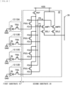
- a source of the selection transistor SEL1 (an output end of the readout circuit 22) is electrically coupled to the vertical signal line 24, and a gate of the selection transistor SEL1 is electrically coupled to the pixel drive line 23 (see FIG. 1 ).
- a source of the amplification transistor AMP2 is electrically coupled to a drain of the selection transistor SEL2, and a gate of the amplification transistor AMP2 is electrically coupled to the floating diffusion FD2.
- a source of the selection transistor SEL2 (an output end of the readout circuit 22) is electrically coupled to the vertical signal line 24, and a gate of the selection transistor SEL2 is electrically coupled to the pixel drive line 23 (see FIG. 1 ).
- the readout circuit 22 is provided with a signal path P1 including the floating diffusion FD1 and the amplification transistor AMP 1 and with a signal path P2 including the floating diffusion FD2 and the amplification transistor AMP2.
- the signal path P1 corresponds to a specific example of a "first signal path" of the present disclosure.
- the signal path P2 corresponds to a specific example of a "second signal path” of the present disclosure.
- One end of each of the signal paths P1 and P2 is electrically coupled to the vertical signal line 24, the other end of the signal path P1 is electrically coupled to the floating diffusion FD1, and the other end of the signal path P2 is electrically coupled to the floating diffusion FD2.
- the signal paths P1 and P2 are coupled in parallel with each other when the switching transistor FDG is ON.
- the signal path P1 is electrically coupled to the transfer transistor TRG, regardless of ON/OFF of the switching transistor FDG.
- the signal path P2 is electrically coupled to the transfer transistor TRG when the switching transistor FDG is ON, but is electrically separated from the transfer transistor TRG when the switching transistor FDG is OFF. That is, when the switching transistor FDG is OFF, no current flows to the signal path P2.
- the transfer transistor TRG When the transfer transistor TRG is brought into an ON state, the transfer transistor TRG transfers charges of the photodiode PD to the floating diffusion FD1 or the floating diffusion FD2.
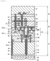
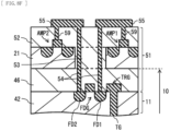
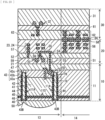
- the gate (a transfer gate TG) of the transfer transistor TRG extends to penetrate a well layer 42 from a top surface of the semiconductor substrate 11 to such a depth as to reach a PD 41, for example, as illustrated in FIG. 3 .
- the reset transistor RST resets an electric potential of each of the floating diffusions FD1 and FD2 to a predetermined electric potential.
- the reset transistor RST is brought into an ON state, the electric potential of each of the floating diffusions FD1 and FD2 is reset to an electric potential of the power source line VDD.
- the selection transistors SEL1 and SEL2 each control an output timing of the pixel signal from the readout circuit 22.
- the amplification transistor AMP1 generates, as a pixel signal, a signal of a voltage corresponding to a level of charges held in the floating diffusion FD 1.
- the amplification transistor AMP2 generates, as a pixel signal, a signal of a voltage corresponding to a level of charges held in the floating diffusion FD2.
- the amplification transistors AMP 1 and AMP2 configure a source-follower type amplifier, and output a pixel signal of a voltage corresponding to a level of charges generated in the photodiode PD.
- the amplification transistor AMP 1 amplifies an electric potential of the floating diffusion FD1, and outputs a voltage corresponding to the electric potential to the column signal processing circuit 34 via the vertical signal line 24.
- the amplification transistor AMP2 amplifies an electric potential of the floating diffusion FD2, and outputs a voltage corresponding to the electric potential to the column signal processing circuit 34 via the vertical signal line 24.
- the switching transistor FDG is used when switching a conversion efficiency.
- the pixel signal is small when shooting in a dark place.
- FD capacity C larger capacity of the floating diffusion FD1
- the pixel signal becomes large in a bright place; it is therefore not possible, for the floating diffusion FD1, to receive the charges of the photodiode PD unless the FD capacity C is large.
- the FD capacity C needs to be large to allow the value V not to be too large (i.e., to be small) upon the conversion to a voltage using the amplification transistor.
- the switching transistor FDG switches the FD capacity C between the time of high-sensitivity low-illuminance mode (first mode) and the time of low-sensitivity high-illuminance mode (second mode). Specifically, the switching transistor FDG is brought into an OFF state to cause the FD capacity C to be relatively small in the first mode, whereas the switching transistor FDG is brought into an ON state to cause the FD capacity C to be relatively large in the second mode.
- the switching transistor FDG, the reset transistor RST, the amplification transistors AMP 1 and AMP2, and the selection transistors SEL1 and SEL2 are each, for example, an NMOS transistor.
- the switching transistor FDG electrically couples the signal path P1 to the photodiode PD and electrically decouples the signal path P2 from the photodiode PD, whereas, in the second mode, the switching transistor FDG electrically couples both of the signal path P1 and the signal path P2 to the photodiode PD. Specifically, the switching transistor FDG is brought into an OFF state in the first mode, and is brought into an ON state in the second mode.
- the PD 41 has an electric conductivity type different from that of the p-well layer 42, and has an electric conductivity type of, for example, an n-type.
- the semiconductor substrate 11 includes, inside the p-well layer 42, the floating diffusions FD1 and FD2 of an electric conductivity type different from that of the p-well layer 42.
- the second substrate 20 has a configuration in which an insulating layer 52 is stacked on the semiconductor substrate 21.
- the second substrate 20 includes the insulating layer 52 as a portion of the interlayer insulating film 51.
- the insulating layer 52 is provided in a gap between the semiconductor substrate 21 and the semiconductor substrate 31.
- the semiconductor substrate 21 is configured by a silicon substrate.
- the second substrate 20 includes, for example, one readout circuit 22 for one sensor pixel 12.
- the second substrate 20 has a configuration in which the readout circuit 22 is provided on a top surface of the semiconductor substrate 21.
- the second substrate 20 is attached to the first substrate 10, with a back surface of the semiconductor substrate 21 being opposed to side of the top surface of the semiconductor substrate 11. That is, the second substrate 20 is attached to the first substrate 10 in a face-to-back manner.
- the second substrate 20 further includes an insulating layer 53 that penetrates the semiconductor substrate 21, in the same layers as the semiconductor substrate 21.
- the second substrate 20 includes the insulating layer 53 as a portion of the interlayer insulating film 51.
- the insulating layer 53 is provided to cover the side surface of a through-wiring line 54 described later.
- a stacked body including the first substrate 10 and the second substrate 20 includes the interlayer insulating film 51 and a plurality of through-wiring lines 54 provided inside the interlayer insulating film 51.
- the plurality of through-wiring lines 54 extend in a normal direction of the semiconductor substrate 21, and is provided to penetrate a location, of the interlayer insulating film 51, including the insulating layer 53.
- the first substrate 10 and the second substrate 20 are electrically coupled to each other by the plurality of through-wiring lines 54.
- two through-wiring lines 54 are electrically coupled to the floating diffusions FD1 and FD2 and a coupling wiring line 55 described later.
- the floating diffusion FD 1 and the gate of the amplification transistor AMP 1 are electrically coupled to each other by the coupling wiring line 55 and the through-wiring line 54.
- the floating diffusion FD2 and the gate of the amplification transistor AMP2 are electrically coupled to each other by the coupling wiring line 55 and the through-wiring line 54.
- the wiring layer 56 further includes, for example, a plurality of pad electrodes 58 inside the insulating layer 57.
- Each of the pad electrodes 58 is formed by Cu (copper), for example.
- Each of the pad electrodes 58 is exposed to a top surface of the wiring layer 56.
- Each of the pad electrodes 58 is used for electric coupling between the second substrate 20 and the third substrate 30 as well as for attaching the second substrate 20 and the third substrate 30 together.
- the plurality of pad electrodes 58 are provided one by one for the respective pixel drive lines 23 and the respective vertical signal lines 24, for example.
- the first substrate 10 and the second substrate 20 are electrically coupled to each other by the through-wiring line 54.
- the second substrate 20 and the third substrate 30 are electrically coupled to each other by bonding between the pad electrodes 58 and 64.
- the through-wiring line 54 has a width that is narrower than a width of a bonded part between the pad electrodes 58 and 64. That is, the through-wiring line 54 has a cross-sectional area that is smaller than a cross-sectional area of the bonded part between the pad electrodes 58 and 64. Accordingly, the through-wiring line 54 does not interfere with higher integration of the sensor pixels 12 inside the first substrate 10.
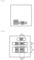
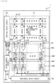
- FIGs. 4 and 5 each illustrate an example of a cross-sectional configuration of the solid-state imaging device 1 in a horizontal direction.
- FIG. 4 illustrates an example of a top surface configuration of the semiconductor substrate 11
- FIG. 5 illustrates an example of a top surface configuration of the semiconductor substrate 21.
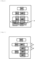
- FIG. 6 illustrates an example of a configuration in which the configuration illustrated in FIG. 4 and the configuration illustrated in FIG. 5 are superimposed on each other.
- the transfer transistor TRG, the switching transistor FDG, and the floating diffusions FD1 and FD2 are provided on the top surface of the semiconductor substrate 11. That is, the transfer transistor TRG, the switching transistor FDG, and the floating diffusions FD 1 and FD2 are provided in the first substrate 10.
- the solid-state imaging device 1 when the configuration illustrated in FIG. 4 and the configuration illustrated in FIG. 5 are superimposed on each other, an overlapping region ⁇ exists. It is appreciated, from the above, that, in the solid-state imaging device 1, as compared with a case where the transfer transistor TRG, the switching transistor FDG and the floating diffusions FD 1 and FD2, the reset transistor RST, the amplification transistors AMP1 and AMP2, and the selection transistors SEL1 and SEL2 are provided in the substrate in common, the solid-state imaging device 1 is miniaturized by the overlapping region ⁇ .
- L lengths b1 and b2 of the amplification transistors AMP1 and AMP2 are equal to each other, for example. Meanwhile, as for W lengths of the amplification transistors AMP1 and AMP2, for example, a W length a2 of the amplification transistor AMP2 is larger than a W length a1 of the amplification transistor AMP 1.
- the W length a2 of the amplification transistor AMP2 is, for example, twice or three times as long as the W length a1 of the amplification transistor AMP 1.
- the W length of the amplification transistor as the readout circuit 22 is the sum of the W length a1 of the amplification transistor AMP1 and the W length a2 of the amplification transistor AMP2.
- performing ON/OF switching of the switching transistor FDG makes it possible, for example, to triple or quadruple the W length of the amplification transistor as the readout circuit 22.
- a plurality of amplification transistors AMP2 may be provided for the readout circuit 22.
- the W length a2 of each of the amplification transistors AMP2 may be equal to the W length a1 of the amplification transistor AMP 1, or may be larger than the W length a1 of the amplification transistor AMP1.
- FIGs. 8A to 8G each illustrate an example of a manufacturing process of the solid-state imaging device 1.
- the p-well layer 42, the element separation section 43, and the p-well layer 44 are formed on the semiconductor substrate 11.
- the photodiode PD, the transfer transistor TRG, the switching transistor FDG, and the floating diffusions FD1 and FD2 are formed on the semiconductor substrate 11 ( FIG. 8A ).
- the insulating layer 46 is formed on the semiconductor substrate 11 ( FIG. 8A ). In this manner, the first substrate 10 is formed.
- the semiconductor substrate 21 is attached onto the first substrate 10 (insulating layer 46) ( FIG. 8B ). At this time, the semiconductor substrate 21 is thinned as necessary. In this occasion, the thickness of the semiconductor substrate 21 is set to be a film thickness necessary for formation of the readout circuit 22.
- the thickness of the semiconductor substrate 21 is typically about several hundred nm. However, depending on the concept of the readout circuit 22, an FD (Fully Depletion) type is also available; in such a case, a range of several nm to several ⁇ m is also employable as the thickness of the semiconductor substrate 21.
- FIG. 15 illustrates a modification example of the circuit configuration of the sensor pixel 12 and the readout circuit 22 of the solid-state imaging device 1 according to the foregoing modification example B.
- four sensor pixels 12 (12A, 12B, 12C, and 12D) share one readout circuit 22.
- the one readout circuit 22 is formed in a region, of the second substrate 20, facing the four sensor pixels 12. Accordingly, as compared with the foregoing embodiment, an area for forming one readout circuit 22 is able to be expanded by four times, thus making it possible to secure an enough space to provide the floating diffusions FD 1 and FD2 and the amplification transistors AMP1 and AMP2. As a result, it is possible to achieve both high sensitivity and a high dynamic range even in a high-definition use application.
- an electrode of each of the transistors formed in the semiconductor substrates 21 and 26 may include a silicide.
- each of the transistors formed in the semiconductor substrates 21 and 26 is formed after the formation of the sensor pixel 12.
- a silicide having low heat resistance for a surface of an impurity diffusion region that is in contact with a source electrode and a drain electrode of each of the transistors included in the readout circuit 22 is possible to use.
- the plurality of through-wiring lines 54, the plurality of through-wiring lines 68, and the plurality of through-wiring lines 67 are arranged in line in a strip shape in the first direction V (a horizontal direction in FIGs. 24 and 25 ) in a plane of the first substrate 10. It is to be noted that FIGs. 24 and 25 each exemplify the case where the plurality of through-wiring lines 54, the plurality of through-wiring lines 68, and the plurality of through-wiring lines 67 are arranged in line in two rows in the first direction V.
- the insulating layer 53 is configured by a plurality of blocks extending in the first direction V.
- the semiconductor substrate 21 extends in the first direction V, and is configured by the plurality of island-shaped blocks 21A arranged side by side in the second direction H orthogonal to the first direction V, with the insulating layer 53 interposed therebetween.
- Each block 21A includes, for example, the reset transistor RST, the amplification transistor AMP, and the selection transistor SEL.
- One readout circuit 22 shared by the four sensor pixels 12 is not arranged to squarely face the four sensor pixels 12, for example, and is arranged to be shifted in the second direction H.
- the one readout circuit 22 shared by the four sensor pixels 12 is configured by the reset transistor RST, the amplification transistor AMP, the selection transistor SEL, and an FD transfer transistor FDG, which are inside a region, of the second substrate 20, shifted in the second direction H from the region facing the four sensor pixels 12.
- the one readout circuit 22 shared by the four sensor pixels 12 is configured by, for example, the amplification transistor AMP, the reset transistor RST, the selection transistor SEL, and the FD transfer transistor FDG inside the one block 21A.
- the one readout circuit 22 shared by the four sensor pixels 12 is not arranged to squarely face the four sensor pixels 12, for example, and is arranged to be shifted in the second direction H from a position squarely facing the four sensor pixels 12.
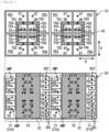
- FIG. 26 illustrates a modification example of the cross-sectional configuration in the horizontal direction of the solid-state imaging device 1 according to any of the modification examples D, J, K, and L.
- An upper drawing in FIG. 26 illustrates an example of the cross-sectional configuration of the first substrate 10 in the solid-state imaging device 1 having the configuration of any of the modification examples D, J, K, and L.
- the upper drawing of FIG. 26 exemplifies a cross-sectional configuration of a location, of the first substrate 10 of the solid-state imaging device 1 having the configuration of any of the modification examples D, J, K, and L, corresponding to the cross-section Sec1 of FIG. 3 . It is to be noted that, in the upper cross-sectional view of FIG.
- FIG. 26 illustrates an example of the cross-sectional configuration of the second substrate 20 in the solid-state imaging device 1 having the configuration of any of the modification examples D, J, K, and L.
- the lower drawing of FIG. 26 exemplifies a cross-sectional configuration of a location, of the second substrate 20 of the solid-state imaging device 1 having the configuration of any of the modification examples D, J, K, and L, corresponding to the cross-section Sec2 of FIG. 3 . It is to be noted that, in the lower cross-sectional view of FIG.
- FIG. 26 exemplifies a configuration in which two sets of four sensor pixels 12 of 2 ⁇ 2 are arranged in the second direction H.
- the semiconductor substrate 21 is configured by the plurality of island-shaped blocks 21A arranged side by side in the first direction V and the second direction H, with the insulating layer 53 interposed therebetween.
- Each block 21A includes, for example, a set of the reset transistor RST, the amplification transistor AMP, and the selection transistor SEL.
- RST reset transistor
- AMP amplification transistor
- SEL selection transistor
- FIG. 27 illustrates a modification example of the cross-sectional configuration in the horizontal direction of the solid-state imaging device 1 according to any of the modification examples D, J, K, L, and M.
- An upper drawing in FIG. 27 illustrates an example of the cross-sectional configuration of the first substrate 10 in the solid-state imaging device 1 having the configuration of any of the modification examples D, J, K, L, and M.
- the upper drawing of FIG. 27 exemplifies a cross-sectional configuration of a location, of the first substrate 10 of the solid-state imaging device 1 having the configuration of any of the modification examples D, J, K, L, and M, corresponding to the cross-section Sec1 of FIG. 3 . It is to be noted that, in the upper cross-sectional view of FIG.
- FIG. 27 illustrates an example of the cross-sectional configuration of the second substrate 20 in the solid-state imaging device 1 having the configuration of any of the modification examples D, J, K, L, and M.
- the lower drawing of FIG. 27 exemplifies a cross-sectional configuration of a location, of the second substrate 20 of the solid-state imaging device 1 having the configuration of any of the modification examples D, J, K, L, and M, corresponding to the cross-section Sec2 of FIG. 3 . It is to be noted that, in the lower cross-sectional view of FIG.
- FIG. 27 exemplifies a configuration in which two sets of four sensor pixels 12 of 2 ⁇ 2 are arranged in the second direction H.
- the one readout circuit 22 shared by the four sensor pixels 12 is not arranged to squarely face the four sensor pixels 12, for example, and is arranged to be shifted in the first direction V.
- the semiconductor substrate 21 is further configured by the plurality of island-shaped blocks 21A arranged side by side in the first direction V and the second direction H, with the insulating layer 53 interposed therebetween.
- Each block 21A includes, for example, a set of the reset transistor RST, the amplification transistor AMP, and the selection transistor SEL.
- the plurality of through-wiring lines 67 and the plurality of through-wiring lines 54 are further arranged also in the second direction H.
- the plurality of through-wiring lines 67 is disposed between the four through-wiring lines 54 sharing a certain readout circuit 22 and the four through-wiring lines 54 sharing another readout circuit 22 adjacent to the certain readout circuit 22 in the second direction H.
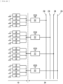
- FIG. 28 illustrates an example of a circuit configuration of the solid-state imaging device 1 according to any of the foregoing embodiment and modification examples thereof.
- the solid-state imaging device 1 according to the present modification example is a CMOS image sensor mounted with a column-parallel ADC.
- the solid-state imaging device 1 is configured to include the vertical drive circuit 33, the column signal processing circuit 34, a reference voltage supply section 38, the horizontal drive circuit 35, a horizontal output line 37, and the system control circuit 36, in addition to the pixel region 13 in which the plurality of sensor pixels 12 each including a photoelectric conversion element are two-dimensionally arranged in matrix (matrix shape).
- the system control circuit 36 on the basis of a master clock MCK, the system control circuit 36 generates a clock signal, a control signal, or the like that serves as a criterion for an operation of the vertical drive circuit 33, the column signal processing circuit 34, the reference voltage supply section 38, the horizontal drive circuit 35, and the like, and provides the clock signal, the control signal, or the like to the vertical drive circuit 33, the column signal processing circuit 34, the reference voltage supply section 38, the horizontal drive circuit 35, and the like.
- the vertical drive circuit 33 is formed in the first substrate 10 together with each of the sensor pixels 12 of the pixel region 13, and is further formed in the second substrate 20, as well, in which the readout circuit 22 is formed.
- the column signal processing circuit 34, the reference voltage supply section 38, the horizontal drive circuit 35, the horizontal output line 37 and the system control circuit 36 are formed in the third substrate 30.
- the sensor pixel 12 for example, a configuration including, in addition to the photodiode PD, the transfer transistor TR that transfers charges obtained by photoelectric conversion in the photodiode PD to the floating diffusion FD, although illustration is omitted here.
- the readout circuit 22 for example, a three-transistor configuration including the reset transistor RST that controls an electric potential of the floating diffusion FD, the amplification transistor AMP that outputs a signal corresponding to an electric potential of the floating diffusion FD, and the selection transistor SEL for selecting a pixel, although illustration is omitted here.
- the sensor pixels 12 are two-dimensionally arranged; with respect to this pixel arrangement of m-row and n-column, the pixel drive lines 23 are wired for respective rows, and the vertical signal lines 24 are wired for respective columns.
- Each one end of the plurality of pixel drive lines 23 is coupled to a corresponding output end of the rows of the vertical drive circuit 33.
- the vertical drive circuit 33 is configured by a shift register or the like, and controls row address and row scanning of the pixel region 13 via the plurality of pixel drive lines 23.
- the reference voltage supply section 38 includes, for example, a DAC (digital-to-analog conversion circuit) 38A as a means to generate a reference voltage Vref of a so-called ramp (RAMP) waveform having a level that changes in an inclined manner as time elapses. It is to be noted that the means to generate the reference voltage Vref of the ramp waveform is not limited to the DAC 38A.
- the DAC 38A Under the control of a control signal CS1 provided from the system control circuit 36, the DAC 38A generates the reference voltage Vref of the ramp waveform on the basis of a clock CK provided from this system control circuit 36 to supply the generated reference voltage Vref to the ADCs 34-1 to 34-m of the column signal processing circuit 34.
- each of the ADCs 34-1 to 34-m is configured to selectively perform an AD conversion operation corresponding to each operation mode of a normal frame rate mode in a progressive scanning system for reading information on all of the sensor pixels 12, and a high-speed frame rate mode for setting exposure time of the sensor pixel 12 to 1/N to increase a frame rate by N times, e.g., by twice, as compared with the time of the normal frame rate mode.
- the switching between the operation modes is executed by controls performed by control signals CS2 and CS3 provided from the system control circuit 36.
- instruction information for switching between the normal frame rate mode and the high-speed frame rate mode is provided from an external system controller (unillustrated) to the system control circuit 36.
- the ADC 34-m is configured to include a comparator 34A, an up/down counter (referred to as U/D CNT in the drawing) 34B as a number-counting means, a transfer switch 34C, and a memory 34D.
- the comparator 34A compares a signal voltage Vx of the vertical signal line 24 corresponding to a signal outputted from each sensor pixel 12 of an n-th column of the pixel region 13 and the reference voltage Vref of the ramp waveform supplied from the reference voltage supply section 38 with each other. For example, when the reference voltage Vref is larger than the signal voltage Vx, an output Vco becomes an "H” level, whereas, when the reference voltage Vref is equal to or less than the signal voltage Vx, the output Vco becomes an "L" level.
- the up/down counter 34B is an asynchronous counter; under the control of the control signal CS2 provided from the system control circuit 36, the up/down counter 34B is provided with the clock CK from the system control circuit 36 simultaneously with the DAC 18A, and performs down (DOWN)-counting or up (UP)-counting in synchronization with the clock CK to thereby measure a comparison period from the start of a comparison operation to the end of the comparison operation in the comparator 34A.
- the down-counting is performed upon a first reading operation to thereby measure comparison time upon the first reading, whereas the up-counting is performed upon a second reading operation to measure comparison time upon the second reading.
- the down-counting is subsequently performed for the sensor pixels 12 of the next row upon the first reading operation from the previous count result to thereby measure the comparison time upon the first reading, and the up-counting is performed upon the second reading operation to thereby measure the comparison time upon the second reading.
- the transfer switch 34C Under the control of the control signal CS3 provided from the system control circuit 36, the transfer switch 34C, in the normal frame rate mode, is brought into an ON (closed) state upon completion of the counting operation of the up/down counter 34B for the sensor pixels 12 of the certain row to transfer, to the memory 34D, the count results of the up/down counter 34B.
- an OFF (open) state remains upon completion of the counting operation of the up/down counter 34B for the sensor pixels 12 of the certain row, and subsequently an ON state is obtained upon completion of the counting operation of the up/down counter 34B for the sensor pixels 12 of the next row to transfer, to the memory 34D, the count results of the up/down counter 34B for the vertical two pixels.
- the horizontal drive circuit 35 is configured by a shift register or the like, and controls column address and column scanning of the ADCs 34-1 to 34-m in the column signal processing circuit 34. Under the control of the horizontal drive circuit 35, the N-bit digital signals having been subjected to the AD conversion in the respective ADCs 34-1 to 34-m are read in order to the horizontal output line 37, and are outputted as imaging data via the horizontal output line 37.
- the count results of the up/down counter 34B are able to be selectively transferred to the memory 34D via the transfer switch 34C. This makes it possible to control the counting operation of the up/down counter 34B and the reading operation of the count results of the up/down counter 34B to the horizontal output line 37 independently of each other.
- FIG. 29 illustrates an example of a configuration of the solid-state imaging device 1 of FIG. 28 , in which three substrates (first substrate 10, second substrate 20, and third substrate 30) are stacked.
- the first substrate 10 has a middle part where the pixel region 13 including the plurality of sensor pixels 12 is formed, with the vertical drive circuit 33 being formed around the pixel region 13.
- the second substrate 20 has a middle part where a readout circuit region 15 including the plurality of readout circuits 22 is formed, with the vertical drive circuit 33 being formed around the readout circuits region 15.
- the column signal processing circuit 34, the horizontal drive circuit 35, the system control circuit 36, the horizontal output line 37, and the reference voltage supply section 38 are formed.
- the solid-state imaging device 1 having a chip size equivalent to an existing chip size and having a three-layered structure not inhibiting the miniaturization of an area per pixel.
- the vertical drive circuit 33 may be formed only in the first substrate 10 or may be formed only in the second substrate 20.
- FIG. 30 illustrates a modification example of the cross-sectional configuration of the solid-state imaging device 1 according to any of the foregoing embodiment and modification examples thereof.
- the third substrate 30 may be omitted, and the logic circuits 32 provided in the third substrate 30 may be formed separately in the first substrate 10 and the second substrate 20, for example, as illustrated in FIG. 30 .
- a circuit 32A, of the logic circuit 32, provided on side of the first substrate 10 is provided with a transistor having a gate structure, in which a high dielectric constant film including a material (e.g., high-k) that is able to withstand a high-temperature process and a metal gate electrode are stacked.
- a material e.g., high-k
- a low-resistance region 27 which includes a silicide formed using a Salicide (Self Aligned Silicide) process such as CoSi 2 and NiSi, on a front surface of an impurity diffusion region in contact with a source electrode and a drain electrode.
- the low-resistance region 27 including a silicide is formed by a compound of a semiconductor substrate material and a metal. This makes it possible to use a high-temperature process such as thermal oxidation when forming the sensor pixel 12.
- FIG. 31 illustrates a modification example of the cross-sectional configuration of the solid-state imaging device 1 according to any of the foregoing embodiment and modification examples thereof.
- a low-resistance region 39 including a silicide formed by using the Salicide (Self Aligned Silicide) process such as CoSi 2 and NiSi may be formed on the front surface of the impurity diffusion region in contact with the source electrode and the drain electrode. This makes it possible to use a high-temperature process such as thermal oxidation when forming the sensor pixel 12.
- Salicide Self Aligned Silicide
- the electric conductivity type may be opposite.
- the p-type may be read as the n-type
- the n-type may be read as the p-type. Even in such a case, it is possible to obtain effects similar to those of the foregoing embodiment and modification examples thereof.
- FIG. 32 illustrates an example of a schematic configuration of an imaging system 2 including the solid-state imaging device 1 according to any of the foregoing embodiment and modification examples thereof.
- the imaging system 2 is an electronic apparatus including, for example, a solid-state imaging apparatus such as a digital still camera or a video camera, or a portable terminal apparatus such as a smartphone or a tablet-type terminal.
- the imaging system 2 includes, for example, the solid-state imaging device 1 according to any of the foregoing embodiment and modification examples thereof, a DSP circuit 141, a frame memory 142, a display unit 143, a storage unit 144, an operation unit 145, and a power source unit 146.
- the solid-state imaging device 1 In the imaging system 2, the solid-state imaging device 1 according to any of the foregoing embodiment and modification examples thereof, the DSP circuit 141, the frame memory 142, the display unit 143, the storage unit 144, the operation unit 145, and the power source unit 146 are coupled to one another via a bus line 147.
- the solid-state imaging device 1 outputs image data corresponding to incident light.
- the DSP circuit 141 is a signal processing circuit that processes a signal (image data) outputted from the solid-state imaging device 1 according to any of the foregoing embodiment and modification examples thereof.
- the frame memory 142 temporarily holds the image data processed by the DSP circuit 141 in a frame unit.
- the display unit 143 includes, for example, a panel-type display device such as a liquid crystal panel or an organic EL (Electro Luminescence) panel, and displays a moving image or a still image captured by the solid-state imaging device 1 according to any of the foregoing embodiment and modification examples thereof.
- the storage unit 144 records image data of a moving image or a still image captured by the solid-state imaging device 1 according to any of the foregoing embodiment and modification examples thereof in a recording medium such as a semiconductor memory or a hard disk.
- the operation unit 145 issues an operation command for various functions of the imaging system 2 in accordance with an operation by a user.
- the power source unit 146 appropriately supplies various types of power for operation to the solid-state imaging device 1 according to any of the foregoing embodiment and modification examples thereof, the DSP circuit 141, the frame memory 142, the display unit 143, the storage unit 144, and the operation unit 145 which are supply targets.
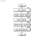
- FIG. 33 illustrates an example of a flowchart of an imaging operation in the imaging system 2.
- a user instructs start of imaging by operating the operation unit 145 (step S101).
- the operation unit 145 transmits an imaging command to the solid-state imaging device 1 (step S102).
- the solid-state imaging device 1 (specifically, the system control circuit 36) executes imaging in a predetermined imaging method upon receiving the imaging command (step S103).
- the driving system control unit 12010 controls the operation of devices related to the driving system of the vehicle in accordance with various kinds of programs.
- the driving system control unit 12010 functions as a control device for a driving force generating device for generating the driving force of the vehicle, such as an internal combustion engine, a driving motor, or the like, a driving force transmitting mechanism for transmitting the driving force to wheels, a steering mechanism for adjusting the steering angle of the vehicle, a braking device for generating the braking force of the vehicle, and the like.
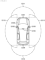
- At least one of the imaging sections 12101 to 12104 may be an infrared camera that detects infrared rays.
- the microcomputer 12051 can, for example, recognize a pedestrian by determining whether or not there is a pedestrian in imaged images of the imaging sections 12101 to 12104. Such recognition of a pedestrian is, for example, performed by a procedure of extracting characteristic points in the imaged images of the imaging sections 12101 to 12104 as infrared cameras and a procedure of determining whether or not it is the pedestrian by performing pattern matching processing on a series of characteristic points representing the contour of the object.
- FIG. 36 is a view depicting an example of a schematic configuration of an endoscopic surgery system to which the technology according to an embodiment of the present disclosure (present technology) can be applied.
- the CCU 11201 includes a central processing unit (CPU), a graphics processing unit (GPU) or the like and integrally controls operation of the endoscope 11100 and a display apparatus 11202. Further, the CCU 11201 receives an image signal from the camera head 11102 and performs, for the image signal, various image processes for displaying an image based on the image signal such as, for example, a development process (demosaic process).
- a development process demosaic process
- the display apparatus 11202 displays thereon an image based on an image signal, for which the image processes have been performed by the CCU 11201, under the control of the CCU 11201.
- the light source apparatus 11203 may be controlled such that the intensity of light to be outputted is changed for each predetermined time.
- driving of the image pickup element of the camera head 11102 in synchronism with the timing of the change of the intensity of light to acquire images time-divisionally and synthesizing the images an image of a high dynamic range free from underexposed blocked up shadows and overexposed highlights can be created.
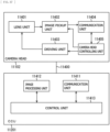
- FIG. 37 is a block diagram depicting an example of a functional configuration of the camera head 11102 and the CCU 11201 depicted in FIG. 36 .
- the driving unit 11403 includes an actuator and moves the zoom lens and the focusing lens of the lens unit 11401 by a predetermined distance along an optical axis under the control of the camera head controlling unit 11405. Consequently, the magnification and the focal point of a picked up image by the image pickup unit 11402 can be adjusted suitably.
- the image pickup conditions such as the frame rate, exposure value, magnification or focal point may be designated by the user or may be set automatically by the control unit 11413 of the CCU 11201 on the basis of an acquired image signal.
- an auto exposure (AE) function, an auto focus (AF) function and an auto white balance (AWB) function are incorporated in the endoscope 11100.
- the image processing unit 11412 performs various image processes for an image signal in the form of RAW data transmitted thereto from the camera head 11102.
- the control unit 11413 performs various kinds of control relating to image picking up of a surgical region or the like by the endoscope 11100 and display of a picked up image obtained by image picking up of the surgical region or the like. For example, the control unit 11413 creates a control signal for controlling driving of the camera head 11102.
- control unit 11413 controls, on the basis of an image signal for which image processes have been performed by the image processing unit 11412, the display apparatus 11202 to display a picked up image in which the surgical region or the like is imaged.
- control unit 11413 may recognize various objects in the picked up image using various image recognition technologies.
- the control unit 11413 can recognize a surgical tool such as forceps, a particular living body region, bleeding, mist when the energy device 11112 is used and so forth by detecting the shape, color and so forth of edges of objects included in a picked up image.
- the control unit 11413 may cause, when it controls the display apparatus 11202 to display a picked up image, various kinds of surgery supporting information to be displayed in an overlapping manner with an image of the surgical region using a result of the recognition. Where surgery supporting information is displayed in an overlapping manner and presented to the surgeon 11131, the burden on the surgeon 11131 can be reduced and the surgeon 11131 can proceed with the surgery with certainty.
- the transmission cable 11400 which connects the camera head 11102 and the CCU 11201 to each other is an electric signal cable ready for communication of an electric signal, an optical fiber ready for optical communication or a composite cable ready for both of electrical and optical communications.
- communication is performed by wired communication using the transmission cable 11400
- the communication between the camera head 11102 and the CCU 11201 may be performed by wireless communication.
- an amplification transistor to be used is selected depending on the mode, and at least the amplification transistor is formed in a substrate different from a substrate in which the photoelectric conversion section is formed, thus making it possible to achieve both high sensitivity and a high dynamic range even in a high-definition use application. It is to be noted that the effects of the present technology are not necessarily limited to the effects described herein, and may have any of the effects described herein.
Landscapes
- Engineering & Computer Science (AREA)
- Multimedia (AREA)
- Signal Processing (AREA)
- Solid State Image Pick-Up Elements (AREA)
- Transforming Light Signals Into Electric Signals (AREA)
Claims (10)
- Festzustandsbildgebungsvorrichtung (1), umfassend:einen photoelektrischen Umwandlungsabschnitt (PD);einen ersten Signalpfad (P1), der eine erste floatende Diffusion (FD1) und einen ersten Verstärkungstransistor (AMP1) umfasst;einen zweiten Signalpfad (P2), der eine zweite floatende Diffusion (FD2) und einen zweiten Verstärkungstransistor (AMP2) umfasst;einen Modusumschaltschalterabschnitt (FDG), der in einem ersten Modus den ersten Signalpfad (P1) mit dem photoelektrischen Umwandlungsabschnitt (PD) elektrisch koppelt und den zweiten Signalpfad (P2) von dem photoelektrischen Umwandlungsabschnitt (PD) elektrisch entkoppelt, und der in einem zweiten Modus sowohl den ersten Signalpfad (P1) als auch den zweiten Signalpfad (P2) mit dem photoelektrischen Umwandlungsabschnitt (PD) elektrisch koppelt;ein erstes Substrat (10), in dem mindestens der photoelektrische Umwandlungsabschnitt (PD) aus der Gruppe aus dem photoelektrischen Umwandlungsabschnitt (PD), der ersten floatenden Diffusion (FD1), dem ersten Verstärkungstransistor (AMP1), der zweiten floatenden Diffusion (FD2), dem zweiten Verstärkungstransistor (AMP2) und dem Modusumschaltschalterabschnitt (FDG) ausgebildet ist; undein zweites Substrat (20), das auf dem ersten Substrat (10) gestapelt ist, und in dem mindestens der zweite Verstärkungstransistor (AMP2) aus der Gruppe aus dem photoelektrischen Umwandlungsabschnitt (PD), der ersten floatenden Diffusion (FD1), dem ersten Verstärkungstransistor (AMP1), der zweiten floatenden Diffusion (FD2), dem zweiten Verstärkungstransistor (AMP2) und dem Modusumschaltschalterabschnitt (FDG) ausgebildet ist.
- Festzustandsbildgebungsvorrichtung (1) nach Anspruch 1, wobeider photoelektrische Umwandlungsabschnitt (PD), die erste floatende Diffusion (FD1), die zweite floatende Diffusion (FD2) und der Modusumschaltschalterabschnitt (FDG) in dem ersten Substrat (10) ausgebildet sind, undder erste Verstärkungstransistor (AMP1) und der zweite Verstärkungstransistor (AMP2) in dem zweiten Substrat (20) ausgebildet sind.
- Festzustandsbildgebungsvorrichtung (1) nach Anspruch 1, wobeider photoelektrische Umwandlungsabschnitt (PD), die erste floatende Diffusion (FD1), der erste Verstärkungstransistor (AMP1), die zweite floatende Diffusion (FD2) und der Modusumschaltschalterabschnitt (FDG) in dem ersten Substrat (10) ausgebildet sind, undder zweite Verstärkungstransistor (AMP2) in dem zweiten Substrat (20) ausgebildet ist.
- Festzustandsbildgebungsvorrichtung (1) nach Anspruch 1, wobeider photoelektrische Umwandlungsabschnitt (PD) in dem ersten Substrat (10) ausgebildet ist, unddie erste floatende Diffusion (FD1), der erste Verstärkungstransistor (AMP1), die zweite floatende Diffusion (FD2), der zweite Verstärkungstransistor (AMP2) und der Modusumschaltschalterabschnitt (FDG) in dem zweiten Substrat ausgebildet sind.
- Festzustandsbildgebungsvorrichtung (1) nach einem der Ansprüche 1 bis 4, wobei eine Elektrode des Transistors, der in dem zweiten Substrat (20) ausgebildet ist, ein Silicid einschließt.
- Festzustandsbildgebungsvorrichtung (1) nach einem der Ansprüche 1 bis 5, ferner umfassend eine Antriebsschaltung (33, 35), die einen Antriebsstrom abhängig von einem Ausmaß einer Größe des Transistors ändert, der durch Umschalten des Modusumschaltschalterabschnitts (FDG) umgewandelt wird.
- Festzustandsbildgebungsvorrichtung (1), umfassend:einen photoelektrischen Umwandlungsabschnitt (PD);einen ersten Signalpfad (P1), der eine erste floatende Diffusion (FD1) und einen ersten Verstärkungstransistor (AMP1) umfasst;einen zweiten Signalpfad (P2), der eine zweite floatende Diffusion (FD2) und einen zweiten Verstärkungstransistor (AMP2) umfasst;einen Modusumschaltschalterabschnitt (FDG), der in einem ersten Modus den ersten Signalpfad (P1) mit dem photoelektrischen Umwandlungsabschnitt (PD) elektrisch koppelt und den zweiten Signalpfad (P2) von dem photoelektrischen Umwandlungsabschnitt (PD) elektrisch entkoppelt, und der in einem zweiten Modus sowohl den ersten Signalpfad (P1) als auch den zweiten Signalpfad (P2) mit dem photoelektrischen Umwandlungsabschnitt (PD) elektrisch koppelt;ein erstes Substrat (10), in dem der photoelektrische Umwandlungsabschnitt (PD) und die erste floatende Diffusion (FD1) ausgebildet sind;ein zweites Substrat (20), das auf dem ersten Substrat (10) gestapelt ist und in dem der erste Verstärkungstransistor (AMP1), die zweite floatende Diffusion (FD2) und der Modusumschaltschalterabschnitt (FDG) ausgebildet sind; undein drittes Substrat (30), das auf dem zweiten Substrat (20) gestapelt ist und in dem der zweite Verstärkungstransistor (AMP2) ausgebildet ist.
- Festzustandsbildgebungsvorrichtung (1) nach Anspruch 7, wobei eine Elektrode jedes der Transistoren, die in dem zweiten Substrat (20) und in dem dritten Substrat (30) ausgebildet sind, ein Silicid einschließt.
- Elektronische Einrichtung (2), umfassend:eine Festzustandsbildgebungsvorrichtung (1) nach Anspruch 1, die ein Pixelsignal ausgibt, das einfallendem Licht entspricht; undeine Signalverarbeitungsschaltung (141), die das Pixelsignal verarbeitet.
- Elektronische Einrichtung (2), umfassend:eine Festzustandsbildgebungsvorrichtung (1) nach Anspruch 7, die ein Pixelsignal ausgibt, das einfallendem Licht entspricht; undeine Signalverarbeitungsschaltung (141), die das Pixelsignal verarbeitet.
Priority Applications (1)
| Application Number | Priority Date | Filing Date | Title |
|---|---|---|---|
| EP24179505.3A EP4411819A3 (de) | 2018-11-13 | 2019-10-29 | Festkörperabbildungsvorrichtung und elektronische vorrichtung |
Applications Claiming Priority (2)
| Application Number | Priority Date | Filing Date | Title |
|---|---|---|---|
| JP2018213147 | 2018-11-13 | ||
| PCT/JP2019/042356 WO2020100577A1 (ja) | 2018-11-13 | 2019-10-29 | 固体撮像装置および電子機器 |
Related Child Applications (1)
| Application Number | Title | Priority Date | Filing Date |
|---|---|---|---|
| EP24179505.3A Division EP4411819A3 (de) | 2018-11-13 | 2019-10-29 | Festkörperabbildungsvorrichtung und elektronische vorrichtung |
Publications (3)
| Publication Number | Publication Date |
|---|---|
| EP3882973A1 EP3882973A1 (de) | 2021-09-22 |
| EP3882973A4 EP3882973A4 (de) | 2022-01-12 |
| EP3882973B1 true EP3882973B1 (de) | 2024-07-03 |
Family
ID=70731995
Family Applications (2)
| Application Number | Title | Priority Date | Filing Date |
|---|---|---|---|
| EP24179505.3A Pending EP4411819A3 (de) | 2018-11-13 | 2019-10-29 | Festkörperabbildungsvorrichtung und elektronische vorrichtung |
| EP19885232.9A Active EP3882973B1 (de) | 2018-11-13 | 2019-10-29 | Festkörperbildgebungsvorrichtung und elektronisches gerät |
Family Applications Before (1)
| Application Number | Title | Priority Date | Filing Date |
|---|---|---|---|
| EP24179505.3A Pending EP4411819A3 (de) | 2018-11-13 | 2019-10-29 | Festkörperabbildungsvorrichtung und elektronische vorrichtung |
Country Status (7)
| Country | Link |
|---|---|
| US (1) | US12262129B2 (de) |
| EP (2) | EP4411819A3 (de) |
| JP (1) | JP7679198B2 (de) |
| KR (1) | KR102761019B1 (de) |
| CN (1) | CN112970115B (de) |
| TW (1) | TWI853847B (de) |
| WO (1) | WO2020100577A1 (de) |
Families Citing this family (11)
| Publication number | Priority date | Publication date | Assignee | Title |
|---|---|---|---|---|
| JP2020088480A (ja) * | 2018-11-19 | 2020-06-04 | ソニーセミコンダクタソリューションズ株式会社 | 固体撮像素子、および、撮像装置 |
| KR102940126B1 (ko) | 2021-03-16 | 2026-03-16 | 삼성전자주식회사 | 이미지 센서 |
| FR3122057B1 (fr) | 2021-04-15 | 2025-01-10 | Pyxalis | Matrice de Pixel à sommation analogique à obturation globale |
| US20240381007A1 (en) * | 2021-05-17 | 2024-11-14 | Sony Semiconductor Solutions Corporation | Solid-state imaging apparatus and electronic apparatus |
| KR20220169592A (ko) * | 2021-06-21 | 2022-12-28 | 삼성전자주식회사 | 이미지 센싱 장치 |
| JP7796492B2 (ja) * | 2021-08-06 | 2026-01-09 | ブリルニクス シンガポール プライベート リミテッド | 固体撮像装置、固体撮像装置の駆動方法、および電子機器 |
| JP2024066609A (ja) * | 2022-11-02 | 2024-05-16 | ソニーセミコンダクタソリューションズ株式会社 | 固体撮像素子 |
| WO2024142692A1 (ja) * | 2022-12-28 | 2024-07-04 | ソニーセミコンダクタソリューションズ株式会社 | 固体撮像装置 |
| WO2024252866A1 (ja) * | 2023-06-06 | 2024-12-12 | ソニーセミコンダクタソリューションズ株式会社 | 光検出装置 |
| CN119997636A (zh) * | 2023-11-07 | 2025-05-13 | 上海华力集成电路制造有限公司 | Cis像素读出电路结构及制造方法 |
| WO2025150439A1 (ja) * | 2024-01-10 | 2025-07-17 | ソニーセミコンダクタソリューションズ株式会社 | 光検出装置 |
Family Cites Families (24)
| Publication number | Priority date | Publication date | Assignee | Title |
|---|---|---|---|---|
| JP3713418B2 (ja) * | 2000-05-30 | 2005-11-09 | 光正 小柳 | 3次元画像処理装置の製造方法 |
| JP3984814B2 (ja) * | 2001-10-29 | 2007-10-03 | キヤノン株式会社 | 撮像素子、その撮像素子を用いた放射線撮像装置及びそれを用いた放射線撮像システム |
| US7335958B2 (en) * | 2003-06-25 | 2008-02-26 | Micron Technology, Inc. | Tailoring gate work-function in image sensors |
| KR100775058B1 (ko) * | 2005-09-29 | 2007-11-08 | 삼성전자주식회사 | 픽셀 및 이를 이용한 이미지 센서, 그리고 상기 이미지센서를 포함하는 이미지 처리 시스템 |
| JP2007228460A (ja) * | 2006-02-27 | 2007-09-06 | Mitsumasa Koyanagi | 集積センサを搭載した積層型半導体装置 |
| JP4693183B2 (ja) * | 2007-03-07 | 2011-06-01 | パナソニック株式会社 | 固体撮像装置の製造方法 |
| JP5215681B2 (ja) * | 2008-01-28 | 2013-06-19 | キヤノン株式会社 | 撮像装置及び撮像システム |
| JP5347283B2 (ja) * | 2008-03-05 | 2013-11-20 | ソニー株式会社 | 固体撮像装置およびその製造方法 |
| JP5482025B2 (ja) * | 2009-08-28 | 2014-04-23 | ソニー株式会社 | 固体撮像装置とその製造方法、及び電子機器 |
| JP5820620B2 (ja) * | 2011-05-25 | 2015-11-24 | オリンパス株式会社 | 固体撮像装置、撮像装置、および信号読み出し方法 |
| JP6045156B2 (ja) * | 2011-05-25 | 2016-12-14 | オリンパス株式会社 | 固体撮像装置 |
| US9257468B2 (en) | 2012-11-21 | 2016-02-09 | Olympus Corporation | Solid-state imaging device, imaging device, and signal reading medium that accumulates an amplified signal without digitization |
| JP5791982B2 (ja) * | 2011-07-06 | 2015-10-07 | オリンパス株式会社 | 固体撮像装置、撮像装置、および信号読み出し方法 |
| JP2013090127A (ja) | 2011-10-18 | 2013-05-13 | Olympus Corp | 固体撮像装置および撮像装置 |
| US8773562B1 (en) * | 2013-01-31 | 2014-07-08 | Apple Inc. | Vertically stacked image sensor |
| JP6300491B2 (ja) * | 2013-11-08 | 2018-03-28 | オリンパス株式会社 | 固体撮像装置および撮像装置 |
| CN111968998B (zh) * | 2014-12-26 | 2024-12-13 | 松下知识产权经营株式会社 | 摄像装置 |
| JP2016149387A (ja) * | 2015-02-10 | 2016-08-18 | ルネサスエレクトロニクス株式会社 | 撮像装置およびその製造方法 |
| ES2843101T3 (es) * | 2016-03-15 | 2021-07-15 | Dartmouth College | Sensor de imagen Quanta con iluminación posterior apilado con lectura de agrupaciones en paralelo |
| US10044960B2 (en) * | 2016-05-25 | 2018-08-07 | Omnivision Technologies, Inc. | Systems and methods for detecting light-emitting diode without flickering |
| US9930274B2 (en) * | 2016-06-30 | 2018-03-27 | Sony Corporation | Sample-and-hold circuit with RTS noise reduction by periodic mode switching |
| US9888197B1 (en) * | 2017-01-04 | 2018-02-06 | Semiconductor Components Industries, Llc | Methods and apparatus for a CMOS image sensor with an in-pixel amplifier |
| CN108337409B (zh) * | 2017-01-19 | 2021-06-22 | 松下知识产权经营株式会社 | 摄像装置及照相机系统 |
| US11431926B2 (en) * | 2018-11-09 | 2022-08-30 | Semiconductor Components Industries, Llc | Image sensors having high dynamic range imaging pixels |
-
2019
- 2019-10-29 JP JP2020555983A patent/JP7679198B2/ja active Active
- 2019-10-29 US US17/291,316 patent/US12262129B2/en active Active
- 2019-10-29 KR KR1020217012707A patent/KR102761019B1/ko active Active
- 2019-10-29 WO PCT/JP2019/042356 patent/WO2020100577A1/ja not_active Ceased
- 2019-10-29 EP EP24179505.3A patent/EP4411819A3/de active Pending
- 2019-10-29 CN CN201980073018.5A patent/CN112970115B/zh active Active
- 2019-10-29 EP EP19885232.9A patent/EP3882973B1/de active Active
- 2019-11-06 TW TW108140199A patent/TWI853847B/zh active
Also Published As
| Publication number | Publication date |
|---|---|
| JPWO2020100577A1 (ja) | 2021-09-30 |
| JP7679198B2 (ja) | 2025-05-19 |
| EP4411819A2 (de) | 2024-08-07 |
| TWI853847B (zh) | 2024-09-01 |
| US20220077207A1 (en) | 2022-03-10 |
| KR102761019B1 (ko) | 2025-02-04 |
| EP3882973A1 (de) | 2021-09-22 |
| TW202029733A (zh) | 2020-08-01 |
| EP4411819A3 (de) | 2024-11-20 |
| KR20210092725A (ko) | 2021-07-26 |
| US12262129B2 (en) | 2025-03-25 |
| WO2020100577A1 (ja) | 2020-05-22 |
| EP3882973A4 (de) | 2022-01-12 |
| CN112970115B (zh) | 2025-09-19 |
| CN112970115A (zh) | 2021-06-15 |
Similar Documents
| Publication | Publication Date | Title |
|---|---|---|
| US12266675B2 (en) | Imaging element | |
| EP3882973B1 (de) | Festkörperbildgebungsvorrichtung und elektronisches gerät | |
| US20250240549A1 (en) | Imaging device | |
| EP3940752B1 (de) | Bilderfassungselement | |
| US12615872B2 (en) | Image sensor and electronic apparatus | |
| US20220021826A1 (en) | Imaging device and electronic apparatus | |
| US12389695B2 (en) | Imaging device | |
| EP3896723B1 (de) | Festkörperbildgebungselement und videoaufzeichnungsvorrichtung | |
| US20210384237A1 (en) | Solid-state imaging element and imaging device | |
| US20210408090A1 (en) | Imaging device | |
| US12119359B2 (en) | Imaging device | |
| US20220157876A1 (en) | Imaging unit, method of manufacturing imaging unit, and semiconductor device | |
| US12501733B2 (en) | Semiconductor device and imaging unit |
Legal Events
| Date | Code | Title | Description |
|---|---|---|---|
| STAA | Information on the status of an ep patent application or granted ep patent |
Free format text: STATUS: THE INTERNATIONAL PUBLICATION HAS BEEN MADE |
|
| PUAI | Public reference made under article 153(3) epc to a published international application that has entered the european phase |
Free format text: ORIGINAL CODE: 0009012 |
|
| STAA | Information on the status of an ep patent application or granted ep patent |
Free format text: STATUS: REQUEST FOR EXAMINATION WAS MADE |
|
| 17P | Request for examination filed |
Effective date: 20210610 |
|
| AK | Designated contracting states |
Kind code of ref document: A1 Designated state(s): AL AT BE BG CH CY CZ DE DK EE ES FI FR GB GR HR HU IE IS IT LI LT LU LV MC MK MT NL NO PL PT RO RS SE SI SK SM TR |
|
| A4 | Supplementary search report drawn up and despatched |
Effective date: 20211209 |
|
| RIC1 | Information provided on ipc code assigned before grant |
Ipc: H04N 5/3745 20110101ALI20211203BHEP Ipc: H04N 5/355 20110101ALI20211203BHEP Ipc: H04N 5/369 20110101ALI20211203BHEP Ipc: H01L 27/146 20060101AFI20211203BHEP |
|
| DAV | Request for validation of the european patent (deleted) | ||
| DAX | Request for extension of the european patent (deleted) | ||
| RIC1 | Information provided on ipc code assigned before grant |
Ipc: H01L 27/146 20060101AFI20231205BHEP |
|
| GRAP | Despatch of communication of intention to grant a patent |
Free format text: ORIGINAL CODE: EPIDOSNIGR1 |
|
| STAA | Information on the status of an ep patent application or granted ep patent |
Free format text: STATUS: GRANT OF PATENT IS INTENDED |
|
| INTG | Intention to grant announced |
Effective date: 20240130 |
|
| GRAS | Grant fee paid |
Free format text: ORIGINAL CODE: EPIDOSNIGR3 |
|
| GRAA | (expected) grant |
Free format text: ORIGINAL CODE: 0009210 |
|
| STAA | Information on the status of an ep patent application or granted ep patent |
Free format text: STATUS: THE PATENT HAS BEEN GRANTED |
|
| P01 | Opt-out of the competence of the unified patent court (upc) registered |
Effective date: 20240502 |
|
| AK | Designated contracting states |
Kind code of ref document: B1 Designated state(s): AL AT BE BG CH CY CZ DE DK EE ES FI FR GB GR HR HU IE IS IT LI LT LU LV MC MK MT NL NO PL PT RO RS SE SI SK SM TR |
|
| REG | Reference to a national code |
Ref country code: CH Ref legal event code: EP |
|
| REG | Reference to a national code |
Ref country code: DE Ref legal event code: R096 Ref document number: 602019054787 Country of ref document: DE |
|
| REG | Reference to a national code |
Ref country code: NL Ref legal event code: FP |
|
| REG | Reference to a national code |
Ref country code: LT Ref legal event code: MG9D |
|
| REG | Reference to a national code |
Ref country code: DE Ref legal event code: R079 Ref document number: 602019054787 Country of ref document: DE Free format text: PREVIOUS MAIN CLASS: H01L0027146000 Ipc: H10F0039180000 |
|
| PG25 | Lapsed in a contracting state [announced via postgrant information from national office to epo] |
Ref country code: PT Free format text: LAPSE BECAUSE OF FAILURE TO SUBMIT A TRANSLATION OF THE DESCRIPTION OR TO PAY THE FEE WITHIN THE PRESCRIBED TIME-LIMIT Effective date: 20241104 |
|
| REG | Reference to a national code |
Ref country code: AT Ref legal event code: MK05 Ref document number: 1700750 Country of ref document: AT Kind code of ref document: T Effective date: 20240703 |
|
| PG25 | Lapsed in a contracting state [announced via postgrant information from national office to epo] |
Ref country code: PT Free format text: LAPSE BECAUSE OF FAILURE TO SUBMIT A TRANSLATION OF THE DESCRIPTION OR TO PAY THE FEE WITHIN THE PRESCRIBED TIME-LIMIT Effective date: 20241104 |
|
| PG25 | Lapsed in a contracting state [announced via postgrant information from national office to epo] |
Ref country code: NO Free format text: LAPSE BECAUSE OF FAILURE TO SUBMIT A TRANSLATION OF THE DESCRIPTION OR TO PAY THE FEE WITHIN THE PRESCRIBED TIME-LIMIT Effective date: 20241003 |
|
| PG25 | Lapsed in a contracting state [announced via postgrant information from national office to epo] |
Ref country code: FI Free format text: LAPSE BECAUSE OF FAILURE TO SUBMIT A TRANSLATION OF THE DESCRIPTION OR TO PAY THE FEE WITHIN THE PRESCRIBED TIME-LIMIT Effective date: 20240703 Ref country code: GR Free format text: LAPSE BECAUSE OF FAILURE TO SUBMIT A TRANSLATION OF THE DESCRIPTION OR TO PAY THE FEE WITHIN THE PRESCRIBED TIME-LIMIT Effective date: 20241004 Ref country code: PL Free format text: LAPSE BECAUSE OF FAILURE TO SUBMIT A TRANSLATION OF THE DESCRIPTION OR TO PAY THE FEE WITHIN THE PRESCRIBED TIME-LIMIT Effective date: 20240703 |
|
| PG25 | Lapsed in a contracting state [announced via postgrant information from national office to epo] |
Ref country code: BG Free format text: LAPSE BECAUSE OF FAILURE TO SUBMIT A TRANSLATION OF THE DESCRIPTION OR TO PAY THE FEE WITHIN THE PRESCRIBED TIME-LIMIT Effective date: 20240703 |
|
| PG25 | Lapsed in a contracting state [announced via postgrant information from national office to epo] |
Ref country code: LV Free format text: LAPSE BECAUSE OF FAILURE TO SUBMIT A TRANSLATION OF THE DESCRIPTION OR TO PAY THE FEE WITHIN THE PRESCRIBED TIME-LIMIT Effective date: 20240703 |
|
| PG25 | Lapsed in a contracting state [announced via postgrant information from national office to epo] |
Ref country code: AT Free format text: LAPSE BECAUSE OF FAILURE TO SUBMIT A TRANSLATION OF THE DESCRIPTION OR TO PAY THE FEE WITHIN THE PRESCRIBED TIME-LIMIT Effective date: 20240703 Ref country code: IS Free format text: LAPSE BECAUSE OF FAILURE TO SUBMIT A TRANSLATION OF THE DESCRIPTION OR TO PAY THE FEE WITHIN THE PRESCRIBED TIME-LIMIT Effective date: 20241103 |
|
| PG25 | Lapsed in a contracting state [announced via postgrant information from national office to epo] |
Ref country code: HR Free format text: LAPSE BECAUSE OF FAILURE TO SUBMIT A TRANSLATION OF THE DESCRIPTION OR TO PAY THE FEE WITHIN THE PRESCRIBED TIME-LIMIT Effective date: 20240703 Ref country code: CZ Free format text: LAPSE BECAUSE OF FAILURE TO SUBMIT A TRANSLATION OF THE DESCRIPTION OR TO PAY THE FEE WITHIN THE PRESCRIBED TIME-LIMIT Effective date: 20240703 |
|
| PG25 | Lapsed in a contracting state [announced via postgrant information from national office to epo] |
Ref country code: RS Free format text: LAPSE BECAUSE OF FAILURE TO SUBMIT A TRANSLATION OF THE DESCRIPTION OR TO PAY THE FEE WITHIN THE PRESCRIBED TIME-LIMIT Effective date: 20241003 Ref country code: ES Free format text: LAPSE BECAUSE OF FAILURE TO SUBMIT A TRANSLATION OF THE DESCRIPTION OR TO PAY THE FEE WITHIN THE PRESCRIBED TIME-LIMIT Effective date: 20240703 |
|
| PG25 | Lapsed in a contracting state [announced via postgrant information from national office to epo] |
Ref country code: RS Free format text: LAPSE BECAUSE OF FAILURE TO SUBMIT A TRANSLATION OF THE DESCRIPTION OR TO PAY THE FEE WITHIN THE PRESCRIBED TIME-LIMIT Effective date: 20241003 Ref country code: PL Free format text: LAPSE BECAUSE OF FAILURE TO SUBMIT A TRANSLATION OF THE DESCRIPTION OR TO PAY THE FEE WITHIN THE PRESCRIBED TIME-LIMIT Effective date: 20240703 Ref country code: NO Free format text: LAPSE BECAUSE OF FAILURE TO SUBMIT A TRANSLATION OF THE DESCRIPTION OR TO PAY THE FEE WITHIN THE PRESCRIBED TIME-LIMIT Effective date: 20241003 Ref country code: LV Free format text: LAPSE BECAUSE OF FAILURE TO SUBMIT A TRANSLATION OF THE DESCRIPTION OR TO PAY THE FEE WITHIN THE PRESCRIBED TIME-LIMIT Effective date: 20240703 Ref country code: IS Free format text: LAPSE BECAUSE OF FAILURE TO SUBMIT A TRANSLATION OF THE DESCRIPTION OR TO PAY THE FEE WITHIN THE PRESCRIBED TIME-LIMIT Effective date: 20241103 Ref country code: HR Free format text: LAPSE BECAUSE OF FAILURE TO SUBMIT A TRANSLATION OF THE DESCRIPTION OR TO PAY THE FEE WITHIN THE PRESCRIBED TIME-LIMIT Effective date: 20240703 Ref country code: GR Free format text: LAPSE BECAUSE OF FAILURE TO SUBMIT A TRANSLATION OF THE DESCRIPTION OR TO PAY THE FEE WITHIN THE PRESCRIBED TIME-LIMIT Effective date: 20241004 Ref country code: FI Free format text: LAPSE BECAUSE OF FAILURE TO SUBMIT A TRANSLATION OF THE DESCRIPTION OR TO PAY THE FEE WITHIN THE PRESCRIBED TIME-LIMIT Effective date: 20240703 Ref country code: ES Free format text: LAPSE BECAUSE OF FAILURE TO SUBMIT A TRANSLATION OF THE DESCRIPTION OR TO PAY THE FEE WITHIN THE PRESCRIBED TIME-LIMIT Effective date: 20240703 Ref country code: CZ Free format text: LAPSE BECAUSE OF FAILURE TO SUBMIT A TRANSLATION OF THE DESCRIPTION OR TO PAY THE FEE WITHIN THE PRESCRIBED TIME-LIMIT Effective date: 20240703 Ref country code: BG Free format text: LAPSE BECAUSE OF FAILURE TO SUBMIT A TRANSLATION OF THE DESCRIPTION OR TO PAY THE FEE WITHIN THE PRESCRIBED TIME-LIMIT Effective date: 20240703 Ref country code: AT Free format text: LAPSE BECAUSE OF FAILURE TO SUBMIT A TRANSLATION OF THE DESCRIPTION OR TO PAY THE FEE WITHIN THE PRESCRIBED TIME-LIMIT Effective date: 20240703 |
|
| REG | Reference to a national code |
Ref country code: DE Ref legal event code: R097 Ref document number: 602019054787 Country of ref document: DE |
|
| PG25 | Lapsed in a contracting state [announced via postgrant information from national office to epo] |
Ref country code: RO Free format text: LAPSE BECAUSE OF FAILURE TO SUBMIT A TRANSLATION OF THE DESCRIPTION OR TO PAY THE FEE WITHIN THE PRESCRIBED TIME-LIMIT Effective date: 20240703 Ref country code: DK Free format text: LAPSE BECAUSE OF FAILURE TO SUBMIT A TRANSLATION OF THE DESCRIPTION OR TO PAY THE FEE WITHIN THE PRESCRIBED TIME-LIMIT Effective date: 20240703 Ref country code: SM Free format text: LAPSE BECAUSE OF FAILURE TO SUBMIT A TRANSLATION OF THE DESCRIPTION OR TO PAY THE FEE WITHIN THE PRESCRIBED TIME-LIMIT Effective date: 20240703 |
|
| PG25 | Lapsed in a contracting state [announced via postgrant information from national office to epo] |
Ref country code: EE Free format text: LAPSE BECAUSE OF FAILURE TO SUBMIT A TRANSLATION OF THE DESCRIPTION OR TO PAY THE FEE WITHIN THE PRESCRIBED TIME-LIMIT Effective date: 20240703 |
|
| PG25 | Lapsed in a contracting state [announced via postgrant information from national office to epo] |
Ref country code: SK Free format text: LAPSE BECAUSE OF FAILURE TO SUBMIT A TRANSLATION OF THE DESCRIPTION OR TO PAY THE FEE WITHIN THE PRESCRIBED TIME-LIMIT Effective date: 20240703 Ref country code: IT Free format text: LAPSE BECAUSE OF FAILURE TO SUBMIT A TRANSLATION OF THE DESCRIPTION OR TO PAY THE FEE WITHIN THE PRESCRIBED TIME-LIMIT Effective date: 20240703 |
|
| PLBE | No opposition filed within time limit |
Free format text: ORIGINAL CODE: 0009261 |
|
| STAA | Information on the status of an ep patent application or granted ep patent |
Free format text: STATUS: NO OPPOSITION FILED WITHIN TIME LIMIT |
|
| REG | Reference to a national code |
Ref country code: CH Ref legal event code: PL |
|
| 26N | No opposition filed |
Effective date: 20250404 |
|
| PG25 | Lapsed in a contracting state [announced via postgrant information from national office to epo] |
Ref country code: MC Free format text: LAPSE BECAUSE OF FAILURE TO SUBMIT A TRANSLATION OF THE DESCRIPTION OR TO PAY THE FEE WITHIN THE PRESCRIBED TIME-LIMIT Effective date: 20240703 |
|
| PG25 | Lapsed in a contracting state [announced via postgrant information from national office to epo] |
Ref country code: LU Free format text: LAPSE BECAUSE OF NON-PAYMENT OF DUE FEES Effective date: 20241029 Ref country code: BE Free format text: LAPSE BECAUSE OF NON-PAYMENT OF DUE FEES Effective date: 20241031 |
|
| PG25 | Lapsed in a contracting state [announced via postgrant information from national office to epo] |
Ref country code: CH Free format text: LAPSE BECAUSE OF NON-PAYMENT OF DUE FEES Effective date: 20241031 |
|
| REG | Reference to a national code |
Ref country code: BE Ref legal event code: MM Effective date: 20241031 |
|
| PG25 | Lapsed in a contracting state [announced via postgrant information from national office to epo] |
Ref country code: SE Free format text: LAPSE BECAUSE OF FAILURE TO SUBMIT A TRANSLATION OF THE DESCRIPTION OR TO PAY THE FEE WITHIN THE PRESCRIBED TIME-LIMIT Effective date: 20240703 |
|
| PGFP | Annual fee paid to national office [announced via postgrant information from national office to epo] |
Ref country code: NL Payment date: 20250923 Year of fee payment: 7 |
|
| PGFP | Annual fee paid to national office [announced via postgrant information from national office to epo] |
Ref country code: GB Payment date: 20250923 Year of fee payment: 7 |
|
| PGFP | Annual fee paid to national office [announced via postgrant information from national office to epo] |
Ref country code: FR Payment date: 20250924 Year of fee payment: 7 |
|
| PG25 | Lapsed in a contracting state [announced via postgrant information from national office to epo] |
Ref country code: IE Free format text: LAPSE BECAUSE OF NON-PAYMENT OF DUE FEES Effective date: 20241029 |
|
| PGFP | Annual fee paid to national office [announced via postgrant information from national office to epo] |
Ref country code: DE Payment date: 20250923 Year of fee payment: 7 |
|
| PG25 | Lapsed in a contracting state [announced via postgrant information from national office to epo] |
Ref country code: HU Free format text: LAPSE BECAUSE OF FAILURE TO SUBMIT A TRANSLATION OF THE DESCRIPTION OR TO PAY THE FEE WITHIN THE PRESCRIBED TIME-LIMIT; INVALID AB INITIO Effective date: 20191029 |
|
| PG25 | Lapsed in a contracting state [announced via postgrant information from national office to epo] |
Ref country code: CY Free format text: LAPSE BECAUSE OF FAILURE TO SUBMIT A TRANSLATION OF THE DESCRIPTION OR TO PAY THE FEE WITHIN THE PRESCRIBED TIME-LIMIT; INVALID AB INITIO Effective date: 20191029 |