EP3882965A1 - Semiconductor device with an electromigration reducing area - Google Patents
Semiconductor device with an electromigration reducing area Download PDFInfo
- Publication number
- EP3882965A1 EP3882965A1 EP20193077.3A EP20193077A EP3882965A1 EP 3882965 A1 EP3882965 A1 EP 3882965A1 EP 20193077 A EP20193077 A EP 20193077A EP 3882965 A1 EP3882965 A1 EP 3882965A1
- Authority
- EP
- European Patent Office
- Prior art keywords
- semiconductor device
- electromigration
- electrode
- bonding surface
- area
- Prior art date
- Legal status (The legal status is an assumption and is not a legal conclusion. Google has not performed a legal analysis and makes no representation as to the accuracy of the status listed.)
- Pending
Links
Images






Classifications
-
- G—PHYSICS
- G01—MEASURING; TESTING
- G01R—MEASURING ELECTRIC VARIABLES; MEASURING MAGNETIC VARIABLES
- G01R27/00—Arrangements for measuring resistance, reactance, impedance, or electric characteristics derived therefrom
- G01R27/02—Measuring real or complex resistance, reactance, impedance, or other two-pole characteristics derived therefrom, e.g. time constant
- G01R27/08—Measuring resistance by measuring both voltage and current
-
- H—ELECTRICITY
- H10—SEMICONDUCTOR DEVICES; ELECTRIC SOLID-STATE DEVICES NOT OTHERWISE PROVIDED FOR
- H10W—GENERIC PACKAGES, INTERCONNECTIONS, CONNECTORS OR OTHER CONSTRUCTIONAL DETAILS OF DEVICES COVERED BY CLASS H10
- H10W72/00—Interconnections or connectors in packages
- H10W72/60—Strap connectors, e.g. thick copper clips for grounding of power devices
-
- G—PHYSICS
- G01—MEASURING; TESTING
- G01R—MEASURING ELECTRIC VARIABLES; MEASURING MAGNETIC VARIABLES
- G01R31/00—Arrangements for testing electric properties; Arrangements for locating electric faults; Arrangements for electrical testing characterised by what is being tested not provided for elsewhere
- G01R31/50—Testing of electric apparatus, lines, cables or components for short-circuits, continuity, leakage current or incorrect line connections
- G01R31/66—Testing of connections, e.g. of plugs or non-disconnectable joints
-
- H—ELECTRICITY
- H10—SEMICONDUCTOR DEVICES; ELECTRIC SOLID-STATE DEVICES NOT OTHERWISE PROVIDED FOR
- H10W—GENERIC PACKAGES, INTERCONNECTIONS, CONNECTORS OR OTHER CONSTRUCTIONAL DETAILS OF DEVICES COVERED BY CLASS H10
- H10W72/00—Interconnections or connectors in packages
- H10W72/071—Connecting or disconnecting
- H10W72/076—Connecting or disconnecting of strap connectors
-
- H—ELECTRICITY
- H10—SEMICONDUCTOR DEVICES; ELECTRIC SOLID-STATE DEVICES NOT OTHERWISE PROVIDED FOR
- H10W—GENERIC PACKAGES, INTERCONNECTIONS, CONNECTORS OR OTHER CONSTRUCTIONAL DETAILS OF DEVICES COVERED BY CLASS H10
- H10W72/00—Interconnections or connectors in packages
- H10W72/30—Die-attach connectors
-
- H—ELECTRICITY
- H10—SEMICONDUCTOR DEVICES; ELECTRIC SOLID-STATE DEVICES NOT OTHERWISE PROVIDED FOR
- H10W—GENERIC PACKAGES, INTERCONNECTIONS, CONNECTORS OR OTHER CONSTRUCTIONAL DETAILS OF DEVICES COVERED BY CLASS H10
- H10W72/00—Interconnections or connectors in packages
- H10W72/01—Manufacture or treatment
- H10W72/015—Manufacture or treatment of bond wires
- H10W72/01515—Forming coatings
-
- H—ELECTRICITY
- H10—SEMICONDUCTOR DEVICES; ELECTRIC SOLID-STATE DEVICES NOT OTHERWISE PROVIDED FOR
- H10W—GENERIC PACKAGES, INTERCONNECTIONS, CONNECTORS OR OTHER CONSTRUCTIONAL DETAILS OF DEVICES COVERED BY CLASS H10
- H10W72/00—Interconnections or connectors in packages
- H10W72/071—Connecting or disconnecting
- H10W72/073—Connecting or disconnecting of die-attach connectors
-
- H—ELECTRICITY
- H10—SEMICONDUCTOR DEVICES; ELECTRIC SOLID-STATE DEVICES NOT OTHERWISE PROVIDED FOR
- H10W—GENERIC PACKAGES, INTERCONNECTIONS, CONNECTORS OR OTHER CONSTRUCTIONAL DETAILS OF DEVICES COVERED BY CLASS H10
- H10W72/00—Interconnections or connectors in packages
- H10W72/071—Connecting or disconnecting
- H10W72/073—Connecting or disconnecting of die-attach connectors
- H10W72/07331—Connecting techniques
-
- H—ELECTRICITY
- H10—SEMICONDUCTOR DEVICES; ELECTRIC SOLID-STATE DEVICES NOT OTHERWISE PROVIDED FOR
- H10W—GENERIC PACKAGES, INTERCONNECTIONS, CONNECTORS OR OTHER CONSTRUCTIONAL DETAILS OF DEVICES COVERED BY CLASS H10
- H10W72/00—Interconnections or connectors in packages
- H10W72/071—Connecting or disconnecting
- H10W72/073—Connecting or disconnecting of die-attach connectors
- H10W72/07331—Connecting techniques
- H10W72/07336—Soldering or alloying
-
- H—ELECTRICITY
- H10—SEMICONDUCTOR DEVICES; ELECTRIC SOLID-STATE DEVICES NOT OTHERWISE PROVIDED FOR
- H10W—GENERIC PACKAGES, INTERCONNECTIONS, CONNECTORS OR OTHER CONSTRUCTIONAL DETAILS OF DEVICES COVERED BY CLASS H10
- H10W72/00—Interconnections or connectors in packages
- H10W72/071—Connecting or disconnecting
- H10W72/075—Connecting or disconnecting of bond wires
-
- H—ELECTRICITY
- H10—SEMICONDUCTOR DEVICES; ELECTRIC SOLID-STATE DEVICES NOT OTHERWISE PROVIDED FOR
- H10W—GENERIC PACKAGES, INTERCONNECTIONS, CONNECTORS OR OTHER CONSTRUCTIONAL DETAILS OF DEVICES COVERED BY CLASS H10
- H10W72/00—Interconnections or connectors in packages
- H10W72/071—Connecting or disconnecting
- H10W72/075—Connecting or disconnecting of bond wires
- H10W72/07531—Techniques
- H10W72/07532—Compression bonding, e.g. thermocompression bonding
- H10W72/07533—Ultrasonic bonding, e.g. thermosonic bonding
-
- H—ELECTRICITY
- H10—SEMICONDUCTOR DEVICES; ELECTRIC SOLID-STATE DEVICES NOT OTHERWISE PROVIDED FOR
- H10W—GENERIC PACKAGES, INTERCONNECTIONS, CONNECTORS OR OTHER CONSTRUCTIONAL DETAILS OF DEVICES COVERED BY CLASS H10
- H10W72/00—Interconnections or connectors in packages
- H10W72/071—Connecting or disconnecting
- H10W72/075—Connecting or disconnecting of bond wires
- H10W72/07551—Connecting or disconnecting of bond wires characterised by changes in properties of the bond wires during the connecting
- H10W72/07555—Connecting or disconnecting of bond wires characterised by changes in properties of the bond wires during the connecting changes in materials
-
- H—ELECTRICITY
- H10—SEMICONDUCTOR DEVICES; ELECTRIC SOLID-STATE DEVICES NOT OTHERWISE PROVIDED FOR
- H10W—GENERIC PACKAGES, INTERCONNECTIONS, CONNECTORS OR OTHER CONSTRUCTIONAL DETAILS OF DEVICES COVERED BY CLASS H10
- H10W72/00—Interconnections or connectors in packages
- H10W72/30—Die-attach connectors
- H10W72/351—Materials of die-attach connectors
- H10W72/352—Materials of die-attach connectors comprising metals or metalloids, e.g. solders
-
- H—ELECTRICITY
- H10—SEMICONDUCTOR DEVICES; ELECTRIC SOLID-STATE DEVICES NOT OTHERWISE PROVIDED FOR
- H10W—GENERIC PACKAGES, INTERCONNECTIONS, CONNECTORS OR OTHER CONSTRUCTIONAL DETAILS OF DEVICES COVERED BY CLASS H10
- H10W72/00—Interconnections or connectors in packages
- H10W72/50—Bond wires
- H10W72/531—Shapes of wire connectors
- H10W72/533—Cross-sectional shape
- H10W72/534—Cross-sectional shape being rectangular
-
- H—ELECTRICITY
- H10—SEMICONDUCTOR DEVICES; ELECTRIC SOLID-STATE DEVICES NOT OTHERWISE PROVIDED FOR
- H10W—GENERIC PACKAGES, INTERCONNECTIONS, CONNECTORS OR OTHER CONSTRUCTIONAL DETAILS OF DEVICES COVERED BY CLASS H10
- H10W72/00—Interconnections or connectors in packages
- H10W72/50—Bond wires
- H10W72/531—Shapes of wire connectors
- H10W72/5363—Shapes of wire connectors the connected ends being wedge-shaped
-
- H—ELECTRICITY
- H10—SEMICONDUCTOR DEVICES; ELECTRIC SOLID-STATE DEVICES NOT OTHERWISE PROVIDED FOR
- H10W—GENERIC PACKAGES, INTERCONNECTIONS, CONNECTORS OR OTHER CONSTRUCTIONAL DETAILS OF DEVICES COVERED BY CLASS H10
- H10W72/00—Interconnections or connectors in packages
- H10W72/50—Bond wires
- H10W72/541—Dispositions of bond wires
- H10W72/5434—Dispositions of bond wires the connected ends being on auxiliary connecting means on bond pads, e.g. on other bond wires
-
- H—ELECTRICITY
- H10—SEMICONDUCTOR DEVICES; ELECTRIC SOLID-STATE DEVICES NOT OTHERWISE PROVIDED FOR
- H10W—GENERIC PACKAGES, INTERCONNECTIONS, CONNECTORS OR OTHER CONSTRUCTIONAL DETAILS OF DEVICES COVERED BY CLASS H10
- H10W72/00—Interconnections or connectors in packages
- H10W72/50—Bond wires
- H10W72/541—Dispositions of bond wires
- H10W72/5445—Dispositions of bond wires being orthogonal to a side surface of the chip, e.g. parallel arrangements
-
- H—ELECTRICITY
- H10—SEMICONDUCTOR DEVICES; ELECTRIC SOLID-STATE DEVICES NOT OTHERWISE PROVIDED FOR
- H10W—GENERIC PACKAGES, INTERCONNECTIONS, CONNECTORS OR OTHER CONSTRUCTIONAL DETAILS OF DEVICES COVERED BY CLASS H10
- H10W72/00—Interconnections or connectors in packages
- H10W72/50—Bond wires
- H10W72/541—Dispositions of bond wires
- H10W72/5453—Dispositions of bond wires connecting between multiple bond pads on a chip, e.g. daisy chain
-
- H—ELECTRICITY
- H10—SEMICONDUCTOR DEVICES; ELECTRIC SOLID-STATE DEVICES NOT OTHERWISE PROVIDED FOR
- H10W—GENERIC PACKAGES, INTERCONNECTIONS, CONNECTORS OR OTHER CONSTRUCTIONAL DETAILS OF DEVICES COVERED BY CLASS H10
- H10W72/00—Interconnections or connectors in packages
- H10W72/50—Bond wires
- H10W72/541—Dispositions of bond wires
- H10W72/547—Dispositions of multiple bond wires
- H10W72/5475—Dispositions of multiple bond wires multiple bond wires connected to common bond pads at both ends of the wires
-
- H—ELECTRICITY
- H10—SEMICONDUCTOR DEVICES; ELECTRIC SOLID-STATE DEVICES NOT OTHERWISE PROVIDED FOR
- H10W—GENERIC PACKAGES, INTERCONNECTIONS, CONNECTORS OR OTHER CONSTRUCTIONAL DETAILS OF DEVICES COVERED BY CLASS H10
- H10W72/00—Interconnections or connectors in packages
- H10W72/50—Bond wires
- H10W72/551—Materials of bond wires
-
- H—ELECTRICITY
- H10—SEMICONDUCTOR DEVICES; ELECTRIC SOLID-STATE DEVICES NOT OTHERWISE PROVIDED FOR
- H10W—GENERIC PACKAGES, INTERCONNECTIONS, CONNECTORS OR OTHER CONSTRUCTIONAL DETAILS OF DEVICES COVERED BY CLASS H10
- H10W72/00—Interconnections or connectors in packages
- H10W72/50—Bond wires
- H10W72/551—Materials of bond wires
- H10W72/552—Materials of bond wires comprising metals or metalloids, e.g. silver
-
- H—ELECTRICITY
- H10—SEMICONDUCTOR DEVICES; ELECTRIC SOLID-STATE DEVICES NOT OTHERWISE PROVIDED FOR
- H10W—GENERIC PACKAGES, INTERCONNECTIONS, CONNECTORS OR OTHER CONSTRUCTIONAL DETAILS OF DEVICES COVERED BY CLASS H10
- H10W72/00—Interconnections or connectors in packages
- H10W72/50—Bond wires
- H10W72/551—Materials of bond wires
- H10W72/552—Materials of bond wires comprising metals or metalloids, e.g. silver
- H10W72/5522—Materials of bond wires comprising metals or metalloids, e.g. silver comprising gold [Au]
-
- H—ELECTRICITY
- H10—SEMICONDUCTOR DEVICES; ELECTRIC SOLID-STATE DEVICES NOT OTHERWISE PROVIDED FOR
- H10W—GENERIC PACKAGES, INTERCONNECTIONS, CONNECTORS OR OTHER CONSTRUCTIONAL DETAILS OF DEVICES COVERED BY CLASS H10
- H10W72/00—Interconnections or connectors in packages
- H10W72/50—Bond wires
- H10W72/551—Materials of bond wires
- H10W72/552—Materials of bond wires comprising metals or metalloids, e.g. silver
- H10W72/5524—Materials of bond wires comprising metals or metalloids, e.g. silver comprising aluminium [Al]
-
- H—ELECTRICITY
- H10—SEMICONDUCTOR DEVICES; ELECTRIC SOLID-STATE DEVICES NOT OTHERWISE PROVIDED FOR
- H10W—GENERIC PACKAGES, INTERCONNECTIONS, CONNECTORS OR OTHER CONSTRUCTIONAL DETAILS OF DEVICES COVERED BY CLASS H10
- H10W72/00—Interconnections or connectors in packages
- H10W72/50—Bond wires
- H10W72/551—Materials of bond wires
- H10W72/552—Materials of bond wires comprising metals or metalloids, e.g. silver
- H10W72/5525—Materials of bond wires comprising metals or metalloids, e.g. silver comprising copper [Cu]
-
- H—ELECTRICITY
- H10—SEMICONDUCTOR DEVICES; ELECTRIC SOLID-STATE DEVICES NOT OTHERWISE PROVIDED FOR
- H10W—GENERIC PACKAGES, INTERCONNECTIONS, CONNECTORS OR OTHER CONSTRUCTIONAL DETAILS OF DEVICES COVERED BY CLASS H10
- H10W72/00—Interconnections or connectors in packages
- H10W72/50—Bond wires
- H10W72/551—Materials of bond wires
- H10W72/553—Materials of bond wires not comprising solid metals or solid metalloids, e.g. polymers, ceramics or liquids
-
- H—ELECTRICITY
- H10—SEMICONDUCTOR DEVICES; ELECTRIC SOLID-STATE DEVICES NOT OTHERWISE PROVIDED FOR
- H10W—GENERIC PACKAGES, INTERCONNECTIONS, CONNECTORS OR OTHER CONSTRUCTIONAL DETAILS OF DEVICES COVERED BY CLASS H10
- H10W72/00—Interconnections or connectors in packages
- H10W72/50—Bond wires
- H10W72/551—Materials of bond wires
- H10W72/555—Materials of bond wires of outermost layers of multilayered bond wires, e.g. material of a coating
-
- H—ELECTRICITY
- H10—SEMICONDUCTOR DEVICES; ELECTRIC SOLID-STATE DEVICES NOT OTHERWISE PROVIDED FOR
- H10W—GENERIC PACKAGES, INTERCONNECTIONS, CONNECTORS OR OTHER CONSTRUCTIONAL DETAILS OF DEVICES COVERED BY CLASS H10
- H10W72/00—Interconnections or connectors in packages
- H10W72/50—Bond wires
- H10W72/59—Bond pads specially adapted therefor
-
- H—ELECTRICITY
- H10—SEMICONDUCTOR DEVICES; ELECTRIC SOLID-STATE DEVICES NOT OTHERWISE PROVIDED FOR
- H10W—GENERIC PACKAGES, INTERCONNECTIONS, CONNECTORS OR OTHER CONSTRUCTIONAL DETAILS OF DEVICES COVERED BY CLASS H10
- H10W72/00—Interconnections or connectors in packages
- H10W72/60—Strap connectors, e.g. thick copper clips for grounding of power devices
- H10W72/651—Materials of strap connectors
- H10W72/652—Materials of strap connectors comprising metals or metalloids, e.g. silver
-
- H—ELECTRICITY
- H10—SEMICONDUCTOR DEVICES; ELECTRIC SOLID-STATE DEVICES NOT OTHERWISE PROVIDED FOR
- H10W—GENERIC PACKAGES, INTERCONNECTIONS, CONNECTORS OR OTHER CONSTRUCTIONAL DETAILS OF DEVICES COVERED BY CLASS H10
- H10W72/00—Interconnections or connectors in packages
- H10W72/60—Strap connectors, e.g. thick copper clips for grounding of power devices
- H10W72/651—Materials of strap connectors
- H10W72/653—Materials of strap connectors not comprising solid metals or solid metalloids, e.g. polymers, ceramics or liquids
-
- H—ELECTRICITY
- H10—SEMICONDUCTOR DEVICES; ELECTRIC SOLID-STATE DEVICES NOT OTHERWISE PROVIDED FOR
- H10W—GENERIC PACKAGES, INTERCONNECTIONS, CONNECTORS OR OTHER CONSTRUCTIONAL DETAILS OF DEVICES COVERED BY CLASS H10
- H10W72/00—Interconnections or connectors in packages
- H10W72/60—Strap connectors, e.g. thick copper clips for grounding of power devices
- H10W72/651—Materials of strap connectors
- H10W72/655—Materials of strap connectors of outermost layers of multilayered strap connectors, e.g. material of a coating
-
- H—ELECTRICITY
- H10—SEMICONDUCTOR DEVICES; ELECTRIC SOLID-STATE DEVICES NOT OTHERWISE PROVIDED FOR
- H10W—GENERIC PACKAGES, INTERCONNECTIONS, CONNECTORS OR OTHER CONSTRUCTIONAL DETAILS OF DEVICES COVERED BY CLASS H10
- H10W72/00—Interconnections or connectors in packages
- H10W72/90—Bond pads, in general
- H10W72/921—Structures or relative sizes of bond pads
- H10W72/923—Bond pads having multiple stacked layers
-
- H—ELECTRICITY
- H10—SEMICONDUCTOR DEVICES; ELECTRIC SOLID-STATE DEVICES NOT OTHERWISE PROVIDED FOR
- H10W—GENERIC PACKAGES, INTERCONNECTIONS, CONNECTORS OR OTHER CONSTRUCTIONAL DETAILS OF DEVICES COVERED BY CLASS H10
- H10W72/00—Interconnections or connectors in packages
- H10W72/90—Bond pads, in general
- H10W72/921—Structures or relative sizes of bond pads
- H10W72/926—Multiple bond pads having different sizes
-
- H—ELECTRICITY
- H10—SEMICONDUCTOR DEVICES; ELECTRIC SOLID-STATE DEVICES NOT OTHERWISE PROVIDED FOR
- H10W—GENERIC PACKAGES, INTERCONNECTIONS, CONNECTORS OR OTHER CONSTRUCTIONAL DETAILS OF DEVICES COVERED BY CLASS H10
- H10W72/00—Interconnections or connectors in packages
- H10W72/90—Bond pads, in general
- H10W72/931—Shapes of bond pads
- H10W72/934—Cross-sectional shape, i.e. in side view
-
- H—ELECTRICITY
- H10—SEMICONDUCTOR DEVICES; ELECTRIC SOLID-STATE DEVICES NOT OTHERWISE PROVIDED FOR
- H10W—GENERIC PACKAGES, INTERCONNECTIONS, CONNECTORS OR OTHER CONSTRUCTIONAL DETAILS OF DEVICES COVERED BY CLASS H10
- H10W72/00—Interconnections or connectors in packages
- H10W72/90—Bond pads, in general
- H10W72/951—Materials of bond pads
- H10W72/952—Materials of bond pads comprising metals or metalloids, e.g. PbSn, Ag or Cu
-
- H—ELECTRICITY
- H10—SEMICONDUCTOR DEVICES; ELECTRIC SOLID-STATE DEVICES NOT OTHERWISE PROVIDED FOR
- H10W—GENERIC PACKAGES, INTERCONNECTIONS, CONNECTORS OR OTHER CONSTRUCTIONAL DETAILS OF DEVICES COVERED BY CLASS H10
- H10W72/00—Interconnections or connectors in packages
- H10W72/90—Bond pads, in general
- H10W72/951—Materials of bond pads
- H10W72/953—Materials of bond pads not comprising solid metals or solid metalloids, e.g. polymers, ceramics or liquids
Definitions
- Arrangements described herein relate generally to a semiconductor device and an inspection device.
- Power modules composed of various semiconductor devices are widely used as core components in power electronics fields, and are being researched and developed for smaller size and higher power. To achieve the smaller size and the higher power, the power modules need to have a higher current density and higher heat resistance performance. However, the increase in the current density and the rise in the operating temperature lead to a concern about occurrence of electromigration.
- a configuration of setting a diameter of wires and a length of a bonding portion of wire bonding to specific dimensions and a configuration of providing a nickel film on an aluminum electrode are disclosed as technologies to reduce the electromigration.
- the conventional technologies there are cases where effective reduction of the occurrence of the electromigration is difficult.
- the arrangements herein are attained in view of the above, and an object thereby is to provide a semiconductor device and an inspection device capable of effectively reducing the occurrence of the electromigration.
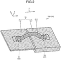
- FIGS. 1 and 2 are schematic views illustrating an example of a semiconductor device 10A according to a first arrangement.
- the semiconductor device 10A and semiconductor devices of the arrangements to be described later may each be called a semiconductor device 10 when they are collectively described.
- the semiconductor device 10A includes a pair of electrodes 16 and conductive connection members 21.
- Each of the pair of electrodes 16 is electrically bonded to the conductive connection members 21 through bonding surfaces 24.
- the bonding surfaces 24 are areas including surfaces on which the electrode 16 is electrically bonded to the conductive connection members 21. That is, each of the bonding surfaces 24 includes a bonding surface of a wiring member 18 bonded to the electrode 16 and a bonding surface of the electrode 16 bonded to the wiring member 18.
- the pair of electrodes 16 are electrically connected onto, for example, a substrate 15.
- the substrate 15 is a substrate including at least one or more layers of each of an electrically insulating layer and an electrically conducting layer.
- the pair of electrodes 16 includes a first electrode 12 and a second electrode 14.
- the present arrangement will be described by way of an example of a configuration in which the first electrode 12 serves as an anode, and the second electrode 14 serves as a cathode.
- a current direction I serving as a direction of a current (electrons) flowing through the wiring member 18 is a direction from the first electrode 12 to the second electrode 14.
- the present arrangement will be described by way of an example in which the current direction I is a direction substantially parallel to an x-axis direction.
- At least the bonding surfaces 24 bonded to the conductive connection members 21 and areas continuing to the bonding surfaces 24 only need to be made of a conductive material.
- the first electrode 12 is a surface electrode of a semiconductor device.
- the surface electrode serving as the first electrode 12 only needs to be bonded to the conductive connection members 21.
- the second electrode 14 is, for example, an electrode of the substrate.
- the electrode of the substrate may be called a substrate electrode. In that case, the substrate electrode only needs to be bonded to the conductive connection members 21.
- a semiconductor of the semiconductor device is made of any semiconductor material, such as Si, Ge, SiC, GaN, SiGe, CdTe, ZnSe, CdS, HgCdTe, CdZnTe, GaAs, GaP, InP, GaAlAs, InGaAs, GaInNAS, or InGaAlP.
- At least a portion of an end face of the semiconductor includes an electrode (semiconductor electrode) serving as the above-mentioned surface electrode.
- the semiconductor electrode is made of any metal material, such as C, W, Cu, Ag, Au, Al, Ni, Pt, Fe, Ti, indium tin oxide (ITO), or ZnO.
- the surface electrode generally has a planar shape.
- a member connected to the surface electrode is not limited to the semiconductor.
- the electrical conductivity of the member connected to the surface electrode only needs to be lower than that of the wiring member 18 and the second electrode 14, and is preferably equal to or lower than half that of the wiring member 18 and the second electrode 14.
- the thickness of the surface electrode only needs to be smaller than the thickness of the second electrode 14, and is preferably equal to or smaller than half the thickness of the second electrode 14.
- the thickness of the surface electrode is, for example, 10 ⁇ m or smaller, but is not limited to this value.
- the surface electrode may be plated.
- the type of the plating is not limited.
- the plating is made of a material, such as Ni, Zn, Cd, ICr, Cu, Ni, Cr, Au, Ag, Pb, or P.
- the substrate electrode serving as the second electrode 14 is made of any metal material, such as C, W, Cu, Ag, Au, Al, Ni, Pt, Fe, Ti, ITO, or ZnO.
- the substrate electrode generally has a planar shape, and generally has a thickness of 10 ⁇ m or larger.
- the second electrode 14 is not limited to the substrate electrode, and may have any shape made of, for example, a metal plate, a metal foil, a reed, a wire, a ribbon, or a bus bar.
- the metal plate, the metal foil, the reed, the wire, the ribbon, or the bus bar forming the substrate electrode may be covered with an insulating material except in portions to be connected to the wiring members 18.
- the metal plate, the metal foil, the reed, the wire, the ribbon, or the bus bar having any shape may be formed in advance before being bonded, or may be formed when being bonded.
- the substrate electrode may be plated.
- the type of the plating is not limited.
- the plating is made of a material, such as Ni, Zn, Cd, ICr, Cu, Ni, Cr, Au, Ag, Pb, or P.
- the conductive connection members 21 are members for electrically bonding the first electrode 12 to the second electrode 14.
- Each of the conductive connection members 21 is, for example, the wiring member 18. In the present arrangement, the case will be described as an example where the conductive connection member 21 is the wiring member 18.
- the wiring member 18 is a member serving as a conductor for conducting electricity between the first electrode 12 and the second electrode 14.
- the wiring member 18 is, for example, a reed, a wire, a ribbon, or a bus bar.
- a constituent material of the wiring member 18 is not limited, and only needs to be a conductive material.
- the wiring member 18 is made of any metal material, such as C, W, Cu, Ag, Au, Al, Ni, Pt, Fe, Ti, ITO, or ZnO.
- the constituent material of the wiring member 18 may be the same as, or different from that of at least one of the first electrode 12 and the second electrode 14.
- the wiring member may be plated.
- the type of the plating is not limited.
- the plating is made of a material, such as Ni, Zn, Cd, ICr, Cu, Ni, Cr, Au, Ag, Pb, or P.
- the constituent material of each of the first electrode 12, the second electrode 14, and the wiring member 18 provided with the electromigration reducing area 22 refers to a material other than an additive to be described later, and corresponds to a base material to be described below. That is, in the present arrangement, the term "base material" is used as a meaning including all of the electrodes, such as the first electrode 12 and the second electrode 14, and the conductive connection member 21 (including the wiring member 18 and a bonding material to be described later).
- the semiconductor device 10A of the present arrangement includes the electromigration reducing areas 22.
- electromigration refers to a phenomenon in which an interaction between atoms in a conductor and electrons passing through the conductor causes the atoms to receive momentum of the electrons to move.
- electromigration refers to a phenomenon in which electrons flowing through a metal collide with metal atoms to transport the metal atoms.
- the transportation of the metal atoms may generate, for example, voids or hillocks.
- the occurrence of the electromigration causes, for example, a disconnection, a short circuit, an insulation failure, and/or an increase in resistance at a portion where the metal atoms are reduced.
- An increase in strain and stress caused by the movement of the metal atoms can lead to mechanical deterioration, such as cracks.
- the electromigration reducing area 22 of the present arrangement is an area for reducing the occurrence of the electromigration.
- the electromigration reducing area 22 is an additive containing area containing the additive.
- the additive is a material for reducing diffusion of the electromigration or reducing the electrical conductivity of the base material of the bonding surface 24.
- the diffusion of the electromigration of the base material refers to at least one of volume diffusion, surface diffusion, grain boundary diffusion, and dislocation diffusion.
- the base material of the bonding surface 24 refers to the constituent material of the wiring member 18 or the electrode 16 included in the bonding surface 24. That is, the electromigration reducing area 22 is an area to which the additive serving as a material different from the base material of the bonding surface 24 has been added.
- the electromigration reducing area 22 is formed by adding the above-described additive to the bonding surface 24. Specifically, the electromigration reducing area 22 is formed by adding the above-described additive to the bonding surface 24 of at least one of the first electrode 12, the second electrode 14, and the wiring member 18. A known method only needs to be used as a method of the addition.
- the additive may be added to at least a portion of the bonding surface 24 in advance before the bonding, or during the bonding, or after the bonding.
- the additive may be added a plurality of times, or may be separately added to a plurality of areas.
- the additive is at least one type selected from the group comprising, for example, Al, Cu, Si, Ni, Cr, Mg, Au, Ag, Ta, Fe, a molybdenum-tungsten alloy (MoW), Ti, Be, Nd, Fr, Nb, and Co.
- MoW molybdenum-tungsten alloy
- the additive is preferably at least one type selected from Cu, Si, Ni, Cr, Mg, Ta, Fe, Ti, Be, Nd, Fr, and Nb, and more preferably at least one type selected from Cu, Si, Ni, Cr, Mg, Ta, Ti, and Be, from the viewpoint of the reduction of the electromigration.
- the type of the additive only needs to be adjusted as appropriate according to the base material of the bonding surface 24 to which the additive is to be added.
- the electromigration reducing area 22 is formed by adding the material different from the base material of the bonding surface 24 as the additive.
- the base material of the bonding surface 24 (that is, the electromigration reducing area 22) is Al.
- the additive contained in the electromigration reducing area 22 is preferably at least either one of at least one type selected from the group comprising Si, Cu, Nd, Mg, Fr, Ti, Mo, Ta, Nb, W, Ni, and Co, and an alloy of at least one type selected from the group and Al.
- the content of the additive in the electromigration reducing area 22 is not limited.
- the content of the additive in the electromigration reducing area 22 is preferably 0.1% or greater by mass and 20.0% or lower by mass, more preferably 0.1% or greater by mass and 10.0% or lower by mass, and particularly preferably 0.1% or greater by mass and 5.0% or lower by mass.
- the electromigration reducing area 22 is provided in at least a portion of a perimeter of the bonding surface 24 of the wiring member 18 bonded to the electrode 16.
- FIG. 3A is a sectional view of the semiconductor device 10A obtained by viewing a dotted line B3 portion of FIG. 3B in a positive y-axis direction.
- the positive y-axis direction refers to a direction from a start point toward an end point of an arrow indicating the y-axis direction in FIG. 3B .
- a mark represented by " ⁇ " in " ⁇ ” represents an arrow in a direction from a start point on the front side of the drawing toward an end point on the back side of the drawing.
- a mark represented by "•" (small filled circle) in “ ⁇ ” represents an arrow in a direction from the start point on the back side of the drawing toward the end point on the front side of the drawing.
- the semiconductor device 10A includes the first electrode 12 serving as the above-mentioned surface electrode (semiconductor electrode) on a portion of an end face of a semiconductor 13.
- the first electrode 12 serving as the above-mentioned surface electrode (semiconductor electrode) on a portion of an end face of a semiconductor 13.
- the second electrode 14 of the semiconductor device 10A is the above-mentioned substrate electrode.
- the bonding surface 24 of the wiring member 18 and the first electrode 12 includes a bonding surface 12A and a bonding surface 18A.
- the bonding surface 12A is the bonding surface 24 of the first electrode 12 bonded to the wiring member 18.
- the bonding surface 18A is the bonding surface 24 of the wiring member 18 bonded to the first electrode 12.
- the bonding surface 24 of the wiring member 18 and the second electrode 14 includes a bonding surface 14B and a bonding surface 18B.
- the bonding surface 14B is the bonding surface 24 of the second electrode 14 bonded to the wiring member 18.
- the bonding surface 18B is the bonding surface 24 of the wiring member 18 bonded to the second electrode 14.
- FIG. 3A illustrates a configuration in which the electromigration reducing area 22 is provided over the whole area of the perimeter of the bonding surface 24 of the wiring member 18.
- the perimeter of the bonding surface 24 refers to an area along the outer circumference of the bonding surface 24.
- FIG. 3B is a sectional view of the semiconductor device 10A obtained by viewing a dotted line A3 portion of FIG. 3A in a positive z-axis direction, and is an explanatory view of a perimeter M of the bonding surface 24.
- the positive z-axis direction refers to a direction from a start point toward an end point of an arrow indicating the z-axis direction in FIG. 3A .
- the perimeter M of the bonding surface 24 refers to an area along an outer circumference P of the bonding surface 24.
- the perimeter M of the bonding surface 24 is a belt-like area having a predetermined width extending toward the inside of the bonding surface 24 from the outer circumference P of the bonding surface 24.
- the perimeter M of the bonding surface 24 only needs to be an area along the outer circumference P of the bonding surface 24, and may include an area having a predetermined width toward the outside of the bonding surface 24 from the outer circumference P of the bonding surface 24 in addition to the belt-like area having the predetermined width extending toward the inside of the bonding surface 24.
- the predetermined width of the perimeter M only needs to be adjusted as appropriate according to, for example, a current intensity applied to the wiring member 18 and a constituent material of the base material of the perimeter M.
- the predetermined width of the perimeter M is preferably 0.1 ⁇ m or greater and 50 ⁇ m or smaller, and is, for example, 0.1 ⁇ m or greater and 5 ⁇ m or smaller, but is not limited to these ranges.
- the electromigration reducing area 22 may be provided in a portion of the perimeter M of each of the bonding surface 18A and the bonding surface 18B.
- FIG. 4A is a sectional view of the semiconductor device 10A obtained by viewing a dotted line B4 portion of FIG. 4B in the positive y-axis direction.
- FIG. 4B is a sectional view of the semiconductor device 10A obtained by viewing a dotted line A4 portion of FIG. 4A in the positive z-axis direction.
- the electromigration reducing area 22 with the above-described additive added thereto is provided in the perimeter M of the bonding surface 18A of the wiring member 18.
- the electromigration reducing area 22 with the above-described additive added thereto is also provided in an end area of the perimeter M of the bonding surface 18B of the wiring member 18, the end area being located on an upstream side in the current direction I of the wiring member 18.
- the electromigration reducing area 22 may be provided in a portion of the perimeter M of the bonding surface 18A.
- the first electrode 12 serving as the semiconductor electrode is provided on the semiconductor 13, while the second electrode 14 is the substrate electrode.
- the inventors of the present invention have found that a current density is more concentrated on the whole perimeter M of the bonding surface 24 as the thickness of the first electrode 12 serving as the surface electrode (semiconductor electrode) is smaller (for example, in the case of a metal foil of 10 ⁇ m or thinner).
- the inventors have found that a current that has flowed from the semiconductor 13 having a larger resistance into the first electrode 12 having a lower resistance and a smaller thickness than the semiconductor 13 is concentrated on the bonding surface 24, and as a result, the current density is concentrated on the whole perimeter M of the bonding surface 24.
- the inventors have also found that the current density is more concentrated on an inside area of the bonding surface 24 when the second electrode 14 serving as the substrate electrode (for example, a metal plate of 10 ⁇ m or thicker) is used.
- the inventors have found that the current density is more concentrated on the inside area of the bonding surface 24 as the thickness of the substrate electrode is larger.
- the inside area refers to an area of the bonding surface 24 on a side facing the other bonding surface 24.
- the electromigration reducing area 22 is preferably provided in the whole area of the perimeter M of the bonding surface 18A constituting the bonding surface 24 bonded to the first electrode 12 serving as the semiconductor electrode among the bonding surfaces 24 of the wiring member 18.
- the electromigration reducing area 22 is also preferably provided at least in an area on the first electrode 12 side of the perimeter M of the bonding surface 18B constituting the bonding surface 24 bonded to the second electrode 14 serving as the substrate electrode among the bonding surfaces 24 of the wiring member 18.
- the length in the current direction I of the electromigration reducing area 22 on the bonding surface 18B only needs to be adjusted as appropriate according to, for example, the current intensity applied to the wiring member 18 and the constituent material of the base material of the bonding surface 18B.
- the length in the current direction I of the electromigration reducing area 22 on the bonding surface 18B is preferably in a range of 0.1 ⁇ m to 50 ⁇ m and more preferably in a range of 0.1 ⁇ m to 5 ⁇ m from the end on the upstream side in the current direction I of the bonding surface 18B.
- the thickness of the electromigration reducing area 22 on each of the bonding surface 18A and the bonding surface 18B of the wiring member 18 is not limited.
- the thickness of the electromigration reducing area 22 refers to a length in a direction orthogonal to the current direction I (in an arrow Z direction in FIG. 4A , which hereinafter, may be called a thickness direction Z) of the wiring member 18.
- the thickness direction Z matches a stacking direction of the electrode 16 and the wiring member 18.
- the thickness of the electromigration reducing area 22 is preferably in a range of 0.1 ⁇ m to 50 ⁇ m, and is, for example, in a range of 0.1 ⁇ m to 5 ⁇ m.
- the thickness of the electromigration reducing area 22 only needs to be adjusted as appropriate according to, for example, the current intensity applied to the wiring member 18, the material of the base material of the electromigration reducing area 22, the type of the additive contained in the electromigration reducing area 22, and the content of the additive.
- the following describes an operation of the semiconductor device 10A of the present arrangement.
- a current flowing through the wiring member 18 is considered to cause the following phenomenon.
- the following description assumes a configuration in which the current flows in the current direction I, with the first electrode 12 side serving as the anode and the second electrode 14 side serving as the cathode.
- the description assumes a comparative semiconductor device having a configuration not provided with the electromigration reducing area 22.
- the comparative semiconductor device has the same configuration as that of the semiconductor device 10, except in not being provided with the electromigration reducing area 22.
- the inventors have found that, when the current flows in the current direction I through the wiring member 18 of the comparative semiconductor device, peaks of the current density, a vacancy concentration, and a hydrostatic stress appear in the perimeter M of the bonding surface 24 (the bonding surface 12A and the bonding surface 18A) of the first electrode 12 serving as the anode and the wiring member 18. This is considered to be because, as described above, the current that has flowed from the semiconductor 13 into the first electrode 12 having the lower resistance and the smaller thickness is concentrated on the bonding surface 24, and as a result, the current density is concentrated on the whole perimeter M of the bonding surface 24.
- the inventors have also found that, when the electromigration reducing area 22 is not provided, the peaks of the current density, the vacancy concentration, and the hydrostatic stress also appear in the end area on the upstream side in the current direction I of the perimeter M of the bonding surface 24 (the bonding surface 14B and the bonding surface 18B) of the second electrode 14 serving as the cathode and the wiring member 18. This is considered to be because, as described above, the current density is more concentrated on the inside area of the bonding surface 24 when the substrate electrode (for example, the metal plate of 10 ⁇ m or thicker) is used as the second electrode 14 serving as the cathode.
- the substrate electrode for example, the metal plate of 10 ⁇ m or thicker
- At least a portion of the perimeter M on each of the bonding surface 18A and the bonding surface 18B of the wiring member 18 serves as the electromigration reducing area 22 formed by adding the additive.
- the additive contained in the electromigration reducing area 22 is considered to restrain at least one of the concentration of the current density, a thermal stress, increase and decrease of the vacancy concentration, and increase and decrease of the hydrostatic stress on each of the bonding surface 18A and the bonding surface 18B of the wiring member 18.
- the semiconductor device 10 of the present arrangement can reduce the occurrence of the electromigration.
- the semiconductor device 10A of the present arrangement includes the pair of electrodes 16 and the wiring member 18 electrically bonded to the pair of electrodes 16.
- at least a portion of the perimeter M of the bonding surface 24 of at least one of the pair of electrodes 16 and the wiring member 18 includes the electromigration reducing area 22.
- the semiconductor device 10A of the present arrangement can restrain at least one of the concentration of the current density, the thermal stress, the increase and decrease of the vacancy concentration, and the increase and decrease of the hydrostatic stress in the perimeter M of the bonding surface 24.
- the semiconductor device 10A of the present arrangement can reduce the occurrence of the electromigration.
- the electromigration reducing area 22 is provided in the area of at least a portion of the perimeter M of the bonding surface 24. With this configuration, the semiconductor device 10A of the present arrangement can reduce the stress and strain caused by the electromigration.
- the semiconductor device 10A of the present arrangement can reduce the occurrence of the electromigration, and can reduce mechanical deterioration.
- the electromigration reducing area 22 is the additive containing area formed by adding the additive to the base material of the perimeter M of the bonding surface 24.
- the electromigration is reduced by adding the additive into the conductor. Adding the additive may, however, reduce the electrical conductivity or reduce the mechanical strength. Since the reduction of the electrical conductivity and the mechanical strength of the electrode 16 and the wiring member 18 directly leads to an increase in power loss and a reduction in mechanical life, the content and the containing portion of the additive are considered to be desirably as small as possible.
- the electromigration reducing area 22 is an area formed by adding the additive to a particular area, such as the area of at least a portion of the perimeter M of the bonding surface 24.
- the semiconductor device 10A of the present arrangement can restrain the electrical resistivity and the mechanical strength of the electrode 16 and the wiring member 18 from being reduced by the addition of the additive, and can reduce the electromigration.
- the additive may be added to at least a portion of the bonding surface 24 of the wiring member 18 in advance before the bonding, or during the bonding, or after the bonding.
- the additive may be added a plurality of times, or may be separately added to a plurality of areas.
- the semiconductor device 10A only needs to have a configuration in which at least a portion of the perimeter M of at least one of the bonding surface 18A and the bonding surface 18B of the wiring member 18 includes the electromigration reducing area 22. Therefore, the electromigration reducing area 22 may be included in at least a portion of the perimeter M of only one of the bonding surface 18A and the bonding surface 18B.
- the configuration has been described as an example in which the portion of the end face of the semiconductor 13 includes the first electrode 12 serving as the above-mentioned surface electrode (semiconductor electrode).
- the case has also been described as an example where the second electrode 14 of the semiconductor device 10 is the substrate electrode.
- the semiconductor device 10 may, however, include both the first electrode 12 and the second electrode 14 as the substrate electrodes.
- FIG. 5 is a sectional view of a semiconductor device 10A' of Modification 1, and illustrates a section in the same position and direction as those in FIG. 3A .
- the semiconductor device 10A' has the same configuration as that of the semiconductor device 10A of the above-described arrangement, except in including a first electrode 12' instead of the first electrode 12.
- the first electrode 12' is the substrate electrode.
- the inventors have found that the current density is more concentrated on the inside area of the bonding surface 24 when the substrate electrode (of, for example, 10 ⁇ m or thicker) is used.
- the electromigration reducing area 22 is preferably provided in at least the inside area of the perimeter M of each of both the bonding surface 18A and the bonding surface 18B.
- FIGS. 6A to 6C is a sectional view of an example in the case where a plurality of the bonding surfaces 24 are present for the wiring member 18 and the electrodes 16, and illustrates a section in the same position and direction as those in FIG. 3B .
- FIG. 6A illustrates, as an example, a case where the semiconductor device 10A has four of the bonding surfaces 24 (bonding surfaces 24A to 24D) from the upstream side toward the downstream side in the current direction I.
- FIG. 6A also illustrates, as an example, a case where the electrode 16 including the bonding surface 24A on the most upstream side in the current direction I serves as a semiconductor electrode 16A.
- FIG. 6A further illustrates, as an example, a case where the electrode 16 including the bonding surfaces 24 (bonding surfaces 24B to 24D) other than the bonding surface 24A on the most upstream side in the current direction I serves as a substrate electrode 16B.
- the inventors have found that the current density is more concentrated on the whole perimeter M of the bonding surface 24 as the thickness of the semiconductor electrode is smaller (for example, 10 ⁇ m or smaller).
- the inventors have also found that the current density is more concentrated on the inside area of the bonding surface 24 when the substrate electrode (of, for example, 10 ⁇ m or thicker) is used.
- the electromigration reducing area 22 is preferably provided in the whole area of the perimeter M of the bonding surface 24A bonded to the semiconductor electrode 16A disposed on the most upstream side in the current direction I.
- the electromigration reducing area 22 is also preferably provided at least in each of the inside areas serving as areas facing the other bonding surfaces 24 in the perimeters M of the bonding surfaces 24 (bonding surfaces 24B to 24D) other than the bonding surface 24A on the most upstream side in the current direction I.
- FIG. 6B illustrates, as an example, the case where the semiconductor device 10A has the four bonding surfaces 24 (bonding surfaces 24A to 24D) from the upstream side toward the downstream side in the current direction I.
- FIG. 6B also illustrates, as an example, a case where the electrode 16 including the bonding surface 24B adjacent on the downstream side to the bonding surface 24A on the most upstream side in the current direction I serves as the semiconductor electrode 16A.
- FIG. 6B further illustrates, as an example, a case where the electrode 16 including the bonding surfaces 24 (bonding surfaces 24A, 24C, and 24D) other than the bonding surface 24B serves as the substrate electrode 16B.
- the electromigration reducing area 22 is preferably provided in the whole area of the perimeter M of the bonding surface 24B bonded to the semiconductor electrode 16A.
- the electromigration reducing area 22 is also preferably provided at least in each of the inside areas serving as areas facing the other bonding surfaces 24 in the perimeters M of the bonding surfaces 24 (bonding surfaces 24A, 24C, and 24D) bonded to the substrate electrode 16B.
- FIG. 6C illustrates, as an example, the case where the semiconductor device 10A has the four bonding surfaces 24 (bonding surfaces 24A to 24D) from the upstream side toward the downstream side in the current direction I.
- FIG. 6C also illustrates, as an example, a case where the electrode 16 including all the bonding surfaces 24 (bonding surfaces 24A to 24B) serves as the substrate electrode 16B.
- the electromigration reducing area 22 is preferably provided at least in each of the inside areas serving as areas facing the other bonding surfaces 24 in the perimeters M of all the bonding surfaces 24A to 24D serving as the bonding surfaces 24 bonded to the substrate electrode 16B.
- the electromigration reducing area 22 is provided on the electrode 16 side.
- the electromigration reducing area 22 is the additive containing area containing the above-described additive.
- FIG. 7A is a sectional view of a semiconductor device 10B obtained by viewing a dotted line B7 portion of FIG. 7B in the positive y-axis direction.
- FIG. 7B is a sectional view of the semiconductor device 10B obtained by viewing a dotted line A7 portion of FIG. 7A in a negative z-axis direction.
- the negative z-axis direction refers to a direction from the end point toward the start point of the arrow indicating the z-axis direction in FIG. 7A .
- the semiconductor device 10B is an example of the semiconductor device 10. Parts having the same configuration as those of the first arrangement will be denoted by the same reference numerals, and will not be described in detail.
- FIG. 7A is a sectional view of the semiconductor device 10B.
- FIG. 7B is a plan view of the semiconductor device 10B.
- the semiconductor device 10B includes the pair of electrodes 16 (the first electrode 12 and the second electrode 14), and the wiring member 18.
- the semiconductor device 10B includes the first electrode 12 serving as the above-mentioned surface electrode (semiconductor electrode) on the portion of the end face of the semiconductor 13.
- the second electrode 14 of the semiconductor device 10B is the above-mentioned substrate electrode.
- the semiconductor device 10B has the same configuration as that of the semiconductor device 10 of the first arrangement, except that the electromigration reducing area 22 is provided in a different position.
- the electromigration reducing area 22 with the above-described additive added thereto is provided in each of the bonding surfaces 24 (the bonding surface 12A and the bonding surface 14B) of the electrodes 16 (the first electrode 12 and the second electrode 14).
- the electromigration reducing area 22 with the above-described additive added thereto is provided in the perimeter M of the bonding surface 12A of the first electrode 12.
- the electromigration reducing area 22 with the above-described additive added thereto is also provided in an end area of the perimeter M of the bonding surface 14B, the end area being located on the upstream side in the current direction I of the wiring member 18.
- the electromigration reducing area 22 may be provided in the whole area of the perimeter M of each of both the bonding surface 12A and the bonding surface 14B.
- the electromigration reducing area 22 may be provided in a portion of the perimeter M of the bonding surface 12A.
- the inventors have found that the current density is more concentrated on the whole perimeter M of the bonding surface 24 as the thickness of the first electrode 12 serving as the surface electrode (semiconductor electrode) is smaller. The inventors have also found that the current density is more concentrated on the inside area of the bonding surface 24 when the substrate electrode is used.
- the electromigration reducing area 22 is preferably provided in the whole area of the perimeter M of the bonding surface 12A constituting the bonding surface 24 bonded to the first electrode 12 serving as the thin semiconductor electrode among the bonding surfaces 24 of the wiring member 18.
- the electromigration reducing area 22 is also preferably provided in at least an area on the first electrode 12 side of the perimeter M of the bonding surface 14B constituting the bonding surface 24 bonded to the second electrode 14 serving as the substrate electrode among the bonding surfaces 24 of the wiring member 18.
- the length in the current direction I of the electromigration reducing area 22 on the bonding surface 14B only needs to be adjusted as appropriate according to, for example, the current intensity applied to the wiring member 18 and the constituent material of the base material of the bonding surface 14B.
- the length in the current direction I of the electromigration reducing area 22 on the bonding surface 14B is preferably in a range of 0.1 ⁇ m to 50 ⁇ m and more preferably in a range of 0.1 ⁇ m to 5 ⁇ m from the end on the upstream side in the current direction I of the bonding surface 14B.
- the thickness of the electromigration reducing area 22 on each of the bonding surface 12A and the bonding surface 14B of the electrode 16 is not limited.
- the thickness of the electromigration reducing area 22 on the electrode 16 only needs to be the same as that in the first arrangement.
- the following describes an operation of the semiconductor device 10B of the present arrangement.
- a current flowing through the wiring member 18 is considered to cause the following phenomenon.
- the following description assumes the configuration in which the current flows in the current direction I, with the first electrode 12 side serving as the anode and the second electrode 14 side serving as the cathode.
- the peaks of the current density, the vacancy concentration, and the hydrostatic stress appear in the perimeter M of the bonding surface 24 (the bonding surface 12A and the bonding surface 18A) of the first electrode 12 serving as the anode and the wiring member 18.
- the peaks of the current density, the vacancy concentration, and the hydrostatic stress also appear in the end area on the upstream side in the current direction I of the perimeter M of the bonding surface 24 (the bonding surface 14B and the bonding surface 18B) of the second electrode 14 serving as the cathode and the wiring member 18.
- the electromigration reducing area 22 formed by adding the additive is provided in an area of at least a portion of the perimeter M of each of the bonding surface 12A of the first electrode 12 and the bonding surface 14B of the second electrode 14.
- the additive contained in the electromigration reducing area 22 is considered to restrain at least one of the concentration of the current density, the thermal stress, the increase and decrease of the vacancy concentration, and the increase and decrease of the hydrostatic stress on each of the bonding surface 12A of the first electrode 12 and the bonding surface 14B of the second electrode 14.
- the semiconductor device 10B of the present arrangement can reduce the occurrence of the electromigration.
- the semiconductor device 10B of the present arrangement may have a configuration of further including the electromigration reducing area 22 described in the above-described first arrangement in addition to the electromigration reducing area 22. That is, the semiconductor device 10B may have a configuration of having the electromigration reducing areas 22 in both the bonding surface 24 on the electrode 16 side and the bonding surface 24 on the wiring member 18 side.
- the case has been described as an example where the first electrode 12 serves as the semiconductor electrode stacked on the semiconductor 13, and the second electrode 14 serves as the substrate electrode.
- the semiconductor device 10B may include both the first electrode 12 and the second electrode 14 as the substrate electrodes (refer to FIG. 5 ).
- the electromigration reducing area 22 is preferably provided at least in an area facing the other bonding surface 24 in a portion of the perimeter M on the bonding surface 24 of each of the first electrode 12 and the second electrode 14 serving as the substrate electrodes.
- the additive may be added to at least a portion of the bonding surface 24 of the electrode 16 in advance before the bonding, or during the bonding, or after the bonding.
- the additive may be added a plurality of times, or may be separately added to a plurality of areas.
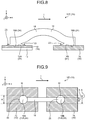
- FIG. 8 is a sectional view of a semiconductor device 10C according to a third arrangement, and illustrates a section in the same position and direction as those in FIG. 3B .
- a configuration will be described in which the bonding surface 24 of the wiring member 18 has a specific shape, and an area having the specific shape serves as an electromigration reducing area 23.
- Parts having the same configuration as those of the first arrangement will be denoted by the same reference numerals, and will not be described in detail.
- the semiconductor device 10C includes the pair of electrodes 16 (the first electrode 12 and the second electrode 14), and the wiring member 18.
- the semiconductor device 10C includes the first electrode 12 serving as the above-mentioned surface electrode (semiconductor electrode) on the portion of the end face of the semiconductor 13.
- the second electrode 14 is the substrate electrode.
- the semiconductor device 10C has the same configuration as that of the semiconductor device 10A of the first arrangement, except in including the electromigration reducing area 23 instead of the electromigration reducing area 22.
- the electromigration reducing area 23 is an area in which a sectional shape of at least a portion of the perimeter M of at least one of the bonding surface 18A and the bonding surface 18B of the wiring member 18 is a fillet shape.
- the electromigration reducing area 23 serving as a fillet-shaped area is specifically an area having a circular arc sectional shape.
- the fillet shape may be called a shape broader downward.
- the sectional shape refers to a shape of a section obtained by cutting the wiring member 18 in the thickness direction Z.
- the definition of the thickness direction Z is the same as that in the above-described arrangements.
- the perimeter M of the bonding surface 18A of the wiring member 18 serves as the electromigration reducing area 23 that is the fillet-shaped area.
- the end area of the perimeter M of the bonding surface 18B of the wiring member 18 located on the upstream side in the current direction I of the wiring member 18 also serves as the electromigration reducing area 23 that is the fillet-shaped area.
- the whole circumference of the perimeter M of each of both the bonding surface 18A and the bonding surface 18B may have the fillet shape such that the whole area of the perimeter M serves as the electromigration reducing area 23.
- a portion of the perimeter M of the bonding surface 18A may have the fillet shape such that the area having the fillet shape serves as the electromigration reducing area 23.
- the semiconductor device 10C of the present arrangement includes the first electrode 12 serving as the above-mentioned surface electrode (semiconductor electrode) on the portion of the end face of the semiconductor 13 while the second electrode 14 is the substrate electrode.
- the whole circumference of the perimeter M of the bonding surface 18A constituting the bonding surface 24 bonded to the first electrode 12 among the bonding surfaces 24 of the wiring member 18 preferably has the fillet shape.
- At least a portion on the first electrode 12 side of the perimeter M of the bonding surface 18B constituting the bonding surface 24 bonded to the second electrode 14 also preferably has the fillet shape.
- the fillet shape may be formed when the wiring member 18 is ultrasonically bonded to the electrode 16.
- each of the bonding surface 18A and the bonding surface 18B of the wiring member 18 may be formed in advance into the fillet shape, and then, bonded to the electrode 16.
- a convex portion to constitute the fillet-shaped electromigration reducing area 23 may be formed in advance on the bonding surface 24 on the electrode 16 side, and then, each of the bonding surface 18A and the bonding surface 18B of the wiring member 18 may be bonded to the convex portion to form the electromigration reducing area 23.
- the following describes an operation of the semiconductor device 10C of the present arrangement.
- a current flowing through the wiring member 18 is considered to cause the following phenomenon.
- the following description assumes the configuration in which the current flows in the current direction I, with the first electrode 12 side serving as the anode and the second electrode 14 side serving as the cathode.
- the peaks of the current density, the vacancy concentration, and the hydrostatic stress appear in the perimeter M of the bonding surface 24 (the bonding surface 12A and the bonding surface 18A) of the first electrode 12 serving as the anode and the wiring member 18.
- the peaks of the current density, the vacancy concentration, and the hydrostatic stress also appear in the end area on the upstream side in the current direction I of the perimeter M of the bonding surface 24 (the bonding surface 14B and the bonding surface 18B) of the second electrode 14 serving as the cathode and the wiring member 18.
- each of the bonding surface 18A and the bonding surface 18B of the wiring member 18 serves as the electromigration reducing area 23 having the fillet shape.
- having the fillet shape is considered to allow the electromigration reducing area 23 to restrain at least one of the concentration of the current density, the thermal stress, the increase and decrease of the vacancy concentration, and the increase and decrease of the hydrostatic stress on each of the bonding surface 18A and the bonding surface 18B of the wiring member 18.
- the semiconductor device 10C of the present arrangement can reduce the occurrence of the electromigration.
- the semiconductor device 10C of the present arrangement may have a configuration of further including the electromigration reducing area 22 described in the above-described arrangements in addition to the electromigration reducing area 23.
- the configuration has been described in which the first electrode 12 serving as the above-mentioned surface electrode (semiconductor electrode) is included in the portion of the end face of the semiconductor 13.
- the case has been described as an example where the second electrode 14 is the substrate electrode.
- the semiconductor device 10C may include both the first electrode 12 and the second electrode 14 as the substrate electrodes (refer to FIG. 5 ) .
- At least areas of the perimeters M facing the other bonding surfaces 24 preferably have the fillet shape.
- FIG. 9 is a view of a semiconductor device 10D according to a fourth arrangement as viewed in the negative z-axis direction from a viewpoint distant in the positive z-axis direction.
- a configuration will be described in which both ends in the current direction I of the wiring member 18 have a specific size to each serve as an electromigration reducing area 25.
- Parts having the same configuration as those of the first arrangement will be denoted by the same reference numerals, and will not be described in detail.
- the semiconductor device 10D includes the pair of electrodes 16 (the first electrode 12 and the second electrode 14), and the wiring member 18.
- the semiconductor device 10D includes the first electrode 12 serving as the above-mentioned surface electrode (semiconductor electrode) on the portion of the end face of the semiconductor 13.
- FIG. 9 does not illustrate the semiconductor 13.
- the second electrode 14 is the substrate electrode. Both the first electrode 12 and the second electrode 14 may be the substrate electrodes in the same way as in the above-described arrangements.
- the semiconductor device 10D has the same configuration as that of the semiconductor device 10A of the first arrangement, except in including the electromigration reducing area 25 instead of the electromigration reducing area 22.
- the electromigration reducing area 25 is an area including the perimeter M of at least one of the bonding surface 18A and the bonding surface 18B of the wiring member 18, and is an area larger than a sectional area of a body of the wiring member 18.
- the body of the wiring member 18 refers to a central portion in the current direction I of the wiring member 18.
- the sectional area refers to an area of an orthogonal section orthogonal to the current direction I of the current flowing through the wiring member 18.
- the sectional area of the bonding surface 18A of the wiring member 18 is, for example, a sectional area of a circular area having a diameter A' in FIG. 9 .
- the sectional area of the bonding surface 18B of the wiring member 18 is, for example, a sectional area of a circular area having a diameter A in FIG. 9 .
- the sectional area of the body of the wiring member 18 is, for example, a sectional area of a circular area having a diameter B in FIG. 9 .
- the sectional shape of the bonding surface 18A, the bonding surface 18B, and the body of the wiring member 18 along the current direction I is not limited to the circular shape.
- the sectional area of the electromigration reducing area 25 only needs to be larger than that of the body of the wiring member 18, and is preferably 1.1 to 5 times and more preferably 1.5 to 3 times that of the body of the wiring member 18.
- the electromigration reducing area 25 may be formed when the wiring member 18 is ultrasonically bonded to the electrode 16.
- each of the bonding surface 18A and the bonding surface 18B of the wiring member 18 may be formed into a shape larger than the body of the wiring member 18, and then, bonded to the electrode 16.
- a convex portion to constitute the electromigration reducing area 25 may be formed in advance on the bonding surface 24 on the electrode 16 side, and then, each of the bonding surface 18A and the bonding surface 18B of the wiring member 18 may be bonded to the convex portion to form the electromigration reducing area 25.
- a current flowing through the wiring member 18 is considered to cause the following phenomenon.
- the following description assumes the configuration in which the current flows in the current direction I, with the first electrode 12 side serving as the anode and the second electrode 14 side serving as the cathode.
- the electromigration reducing area 23 As described in the first arrangement, when the current flows in the current direction I through the wiring member 18 of the comparative semiconductor device provided with none of the electromigration reducing area 22, the electromigration reducing area 23, and the electromigration reducing area 25, the peaks of the current density, the vacancy concentration, and the hydrostatic stress appear in the perimeter M of the bonding surface 24 (the bonding surface 12A and the bonding surface 18A) of the first electrode 12 serving as the anode and the wiring member 18.
- the electromigration reducing area 22 When none of the electromigration reducing area 22, the electromigration reducing area 23, and the electromigration reducing area 25 is provided, the peaks of the current density, the vacancy concentration, and the hydrostatic stress also appear in the end area on the upstream side in the current direction I of the perimeter M of the bonding surface 24 (the bonding surface 14B and the bonding surface 18B) of the second electrode 14 serving as the cathode and the wiring member 18.
- the area including the perimeter M of each of the bonding surface 18A and the bonding surface 18B of the wiring member 18 has a sectional area larger than that of the body of the wiring member 18.
- This configuration is considered to restrain at least one of the concentration of the current density, the thermal stress, the increase and decrease of the vacancy concentration, and the increase and decrease of the hydrostatic stress on each of the bonding surface 18A and the bonding surface 18B of the wiring member 18.
- the semiconductor device 10D of the present arrangement can reduce the occurrence of the electromigration.
- FIG. 10 is a sectional view of a semiconductor device 10E according to a fifth arrangement, and illustrates a section in the same position and direction as those in FIG. 3B .
- a configuration will be described in which an area including the perimeter M of the bonding surface 24 in the electrode 16 is adjusted in thickness to serve as an electromigration reducing area 27 (see C and D).
- Parts having the same configuration as those of the first arrangement will be denoted by the same reference numerals, and will not be described in detail.
- the semiconductor device 10E includes the pair of electrodes 16 (the first electrode 12 and the second electrode 14), and the wiring member 18.
- the semiconductor device 10E includes the first electrode 12 serving as the above-mentioned surface electrode (semiconductor electrode) on the portion of the end face of the semiconductor 13.
- the second electrode 14 is the substrate electrode.
- the semiconductor device 10E has the same configuration as that of the semiconductor device 10 of the first arrangement, except in including the electromigration reducing area 27 instead of the electromigration reducing area 22.
- the electromigration reducing area 27 is a portion of the first electrode 12, and is an area including the perimeter M of the bonding surface 12A of the first electrode 12.
- the electromigration reducing area 27 is an area that increases in thickness stepwise or in a continuous manner as it approaches the bonding surface 12A from positions distant from the bonding surface 12A toward the upstream and downstream sides in the current direction I.
- the electromigration reducing area 27 only needs to be provided on at least one of the first electrode 12 and the second electrode 14, and is not limited to the configuration of being provided on only the first electrode 12.
- the first electrode 12 serving as the semiconductor electrode is provided on the semiconductor 13, while the second electrode 14 is the substrate electrode.
- the electromigration reducing area 27 is preferably provided on at least the bonding surface 12A constituting the bonding surface 24 bonded to the first electrode 12 serving as the semiconductor electrode among the bonding surfaces 24 of the wiring member 18.
- the electromigration reducing area 23 the electromigration reducing area 25, and the electromigration reducing area 27, the peaks of the current density, the vacancy concentration, and the hydrostatic stress appear in the perimeter M of the bonding surface 24 (the bonding surface 12A and the bonding surface 18A) of the first electrode 12 serving as the anode and the wiring member 18.
- the electromigration reducing area 22 When none of the electromigration reducing area 22, the electromigration reducing area 23, the electromigration reducing area 25, and the electromigration reducing area 27 is provided, the peaks of the current density, the vacancy concentration, and the hydrostatic stress also appear in the end area on the upstream side in the current direction I of the perimeter M of the bonding surface 24 (the bonding surface 14B and the bonding surface 18B) of the second electrode 14 serving as the cathode and the wiring member 18.
- the semiconductor device 10E of the present arrangement includes the electromigration reducing area 27.
- the electromigration reducing area 27 is a portion of the first electrode 16, and is an area including the perimeter M of the bonding surface 24 of the electrode 16.
- This configuration is considered to restrain at least one of the concentration of the current density, the thermal stress, the increase and decrease of the vacancy concentration, and the increase and decrease of the hydrostatic stress on each of the bonding surface 18A and the bonding surface 18B of the wiring member 18.
- the semiconductor device 10D of the present arrangement can reduce the occurrence of the electromigration.
- the semiconductor device 10E of the present arrangement may have a configuration obtained by further combining the electromigration reducing area 27 with at least one of the electromigration reducing area 22, the electromigration reducing area 23, and the electromigration reducing area 25 described in the above-described arrangements.
- the configuration has been described as an example in which the conductive connection member 21 is the wiring member 18.
- a configuration will be described in which the conductive connection member 21 is the bonding material.
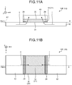
- FIG. 11A is a sectional view illustrating an example of a semiconductor device 10F obtained by viewing a dotted line B11 portion of FIG. 11B in the positive y-axis direction.
- FIG. 11B is a sectional view illustrating the example of the semiconductor device 10F obtained by viewing a dotted line A11 portion of FIG. 11A in the positive z-axis direction (A1).
- the semiconductor device 10F includes a semiconductor 40, a substrate electrode 42, and a bonding material 19.
- the semiconductor device 10F also includes electromigration reducing areas 29.
- the semiconductor 40 is the same as the first electrode 12 of the first arrangement serving as the semiconductor electrode.
- the substrate electrode 42 is the same as the second electrode 14 of the first arrangement serving as the substrate electrode.
- the bonding material 19 is an example of the conductive connection member 21.
- the bonding material 19 is a member for conducting electricity between the semiconductor 40 and the substrate electrode 42.
- the bonding material 19 is, for example, solder.
- the constituent material of the bonding material 19 only needs to be a low melting point material having conductivity, and is not limited.
- the bonding material 19 is made of a material including, for example, Sn, Ag, Cu, Ni, P, Ge, Bi, In, Ni, Sb, or Pb.
- the bonding material is not limited in shape and configuration. Examples of the shape and configuration include a paste, a wire, a plate, a ball, a ribbon, and a chip.
- the shape of the paste, the wire, the plate, the ball, the ribbon, or the chip may be formed in advance, or may be formed when being bonded.
- the solder formed in shape before being bonded is also generally called a preform solder.
- the bonding material 19 may be plated.
- the type of the plating is not limited.
- the plating is made of a material, such as Ni, Zn, Cd, ICr, Cu, Ni, Cr, Au, Ag, Pb, or P.
- the substrate electrode 42 is bonded to the bonding material 19 on a bonding surface 34.
- the bonding surface 34 is an area including a surface of which the bonding material 19 is electrically bonded to the substrate electrode 42.
- the semiconductor 40 is bonded to the bonding material 19 on a bonding surface 35.
- the bonding surface 35 is an area including a surface of which the bonding material 19 is electrically bonded to the semiconductor 40.
- the semiconductor device 10F of the present arrangement includes electromigration reducing areas 29.
- each of the electromigration reducing areas 29 is an area containing a material that reduces the grain boundary diffusion or reduces the electrical conductivity of the base material of the bonding surface 34.
- An example of the additive is the same as the additive of the first arrangement.
- the electromigration reducing areas 29 are provided at all sides of the bonding surface 34 of the bonding material 19 in contact with the substrate electrode 42 through which the current mainly passes. That is, in the semiconductor device 10F of the present arrangement, the electromigration reducing areas 29 are provided in at least portions of the perimeter M of the bonding surface 34.
- the current direction I is a direction from the substrate electrode 42 toward the semiconductor 40.
- the inventors have found that the current density is concentrated on the perimeter M of the bonding surface 34 in the process in which the current flows from the substrate electrode 42 into the bonding material 19.
- the electromigration reducing areas 29 serving as the areas with the additive added thereto are provided in areas of at least the portions of the perimeter M of the bonding surface 34 of the bonding material 19 bonded to the substrate electrode 42.
- This configuration allows the semiconductor device 10F to reduce the occurrence of the electromigration in the same way as in the above-described arrangements.
- the configuration has been described as an example in which the electromigration reducing areas 29 are provided in at least the portions of the perimeter M of the bonding surface 34.
- the configuration may be such that the electromigration reducing areas 29 are provided in at least portions of the perimeters M of the bonding surface 34 and the bonding surface 35.
- the configuration has been described as an example in which the current flows into the bonding material 19 only from the x-axis direction.
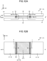
- the electromigration reducing areas 29 are preferably provided in at least portions of ends in the y-axis direction of the perimeter M of the bonding material 19.
- the electromigration reducing areas 29 are preferably provided in at least portions of ends in both the x-axis direction and the y-axis direction of the perimeter M of the bonding material 19.
- the electromigration reducing areas 29 may be provided in at least portions of the ends of the perimeter M.
- the additive may be added to at least portions of the perimeter M of the bonding material 19 in advance before the bonding, or during the bonding, or after the bonding.
- the additive may be added a plurality of times, or may be separately added to a plurality of areas.
- FIG. 12A is a sectional view illustrating an example of a semiconductor device 10F' obtained by viewing a dotted line B12 portion of FIG. 12B in the positive y-axis direction.
- FIG. 12B is a sectional view illustrating the example of the semiconductor device 10F' obtained by viewing a dotted line A12 portion of FIG. 12A in the positive z-axis direction or viewing a dotted line A12' portion in the negative z-axis direction (A2).
- the semiconductor device 10F' differs from the semiconductor device 10F of the sixth arrangement in being provided with a substrate electrode 41 instead of the semiconductor 40.
- the semiconductor device 10F' also differs from the semiconductor device 10F of the sixth arrangement in being provided with the electromigration reducing areas 29 in at least portions of the perimeters M of both the bonding surface 34 and the bonding surface 35. Except in these differences, the semiconductor device 10F' has the same configuration as that of the semiconductor device 10F of the sixth arrangement.
- the electromigration reducing areas 29 are provided on both the bonding surface 34 of the bonding material 19 in contact with the substrate electrode 42 and the bonding surface 35 of the bonding material 19 in contact with the substrate electrode 41.
- the electromigration reducing areas 29 are provided in at least the portions of the perimeters M of both the bonding surface 34 and the bonding surface 35.
- the semiconductor device 10F' can reduce the occurrence of the electromigration in the same way as in the above-described arrangements.
- the configuration has been described as an example in which the current flows into the bonding material 19 from the x-axis direction of both the substrate electrodes 41 and 42.
- the electromigration reducing areas 29 are preferably provided in at least portions of ends in the x-axis direction of the perimeter M of the bonding material 19 on the extending one of the substrate electrodes 41 and 42.
- the electromigration reducing areas 29 are preferably provided in at least portions of ends in the y-axis direction of the perimeter M of the bonding material 19.
- the electromigration reducing areas 29 are preferably provided in at least the portions of the ends in both the x-axis direction and the y-axis direction of the perimeter M of the bonding material 19.
- the electromigration reducing areas 29 may be provided in at least portions of the ends of the perimeter M.
- the additive may be added to at least portions of the perimeter M of the bonding material 19 in advance before the bonding, or during the bonding, or after the bonding.
- the additive may be added a plurality of times, or may be separately added to a plurality of areas.
- a seventh arrangement the following describes an inspection device that inspects deterioration of the conductive connection member 21 of the semiconductor device 10 (any one of the semiconductor devices 10A to 10F') described in the above-described arrangements.
- FIG. 13 is a schematic diagram illustrating an example of an inspection device 1 of the present arrangement.
- the inspection device 1 includes a control device 60, a physical property detection circuit 62, and a storage 64.
- the storage 64 is a memory area including, for example, a dynamic random access memory (DRAM) (including a synchronous dynamic random access memory (SDRAM)) and/or a static random access memory (SRAM).
- DRAM dynamic random access memory
- SDRAM synchronous dynamic random access memory
- SRAM static random access memory
- the storage 64 is, however, not limited to these memories.
- Various storage devices, such as a flash memory, a hard disk drive, and a magnetic tape recorder can be used as the storage 64.
- the storage 64 stores correlation information 64A in advance. Details of the correlation information 64A will be described later.
- the physical property detection circuit 62 is connected to conductive connection members 180 of a plurality of comparative semiconductor devices 100.
- Each of the comparative semiconductor devices 100 has the same configuration as that of the semiconductor device 10 of the above-described arrangements, except in being provided with none of the electromigration reducing areas (the electromigration reducing area 22, the electromigration reducing area 23, the electromigration reducing area 25, the electromigration reducing area 27, and the electromigration reducing areas 29) described in the above-described arrangements.
- the control device 60 may be, for example, an integrated circuit such as a system-on-chip (SoC).
- SoC system-on-chip
- the control device 60 includes a main controller 60A, a digital detection circuit 60B, and a memory controller 60C.
- the main controller 60A, the digital detection circuit 60B, and the memory controller 60C are connected so as to be capable of communicating with one another through, for example, an internal bus (not illustrated).
- the memory controller 60C is configured using, for example, an information processing device such as a digital signal processor (DSP) or a central processing unit (CPU), a memory area such as a random access memory (RAM), and a wireless or wired interface circuit or network interface card (NIC).
- DSP digital signal processor
- CPU central processing unit
- RAM random access memory
- NIC wireless or wired interface circuit or network interface card
- the memory controller 60C controls writing and reading of data to and from the storage 64.
- the digital detection circuit 60B is connected to the physical property detection circuit 62, and converts an analog physical property detection result detected by the physical property detection circuit 62 into a digital physical property detection result.
- FIG. 14 is a block diagram illustrating a functional configuration of the inspection device 1.
- the inspection device 1 includes the storage 64 and a controller 50.
- the controller 50 and the storage 64 are connected so as to be capable of communicating with each other.
- the storage 64 is the same as the above-described storage 64.
- the controller 50 corresponds to the above-described control device 60.
- the controller 50 includes a detector 50A, a deriving unit 50B, and an output controller 50C.
- At least one of the detector 50A, the deriving unit 50B, and the output controller 50C is implemented by, for example, one or a plurality of processors.
- each of the above-mentioned units may be implemented by causing a processor such as a CPU to execute a computer program, that is, by software.
- Each of the above-mentioned units may be implemented by a processor such as a dedicated integrated circuit (IC).
- IC dedicated integrated circuit
- Each of the above-mentioned units may be implemented using both hardware and software.
- each of the processors may implement one of the units, or may implement two or more of the units.
- the detector 50A is connected to the conductive connection members 180 of the comparative semiconductor devices 100.
- the detector 50A detects the physical property of each of the conductive connection members 180 of the comparative semiconductor devices 100.
- the physical property of the conductive connection member 180 refers to at least one of a current flowing through, a voltage across, and an electrical resistance value of the conductive connection member 180, the number of strain cycles in each of a plurality of different directions, the number of stress cycles in each of a plurality of different directions, and the number of temperature cycles.
- the number of cycles refers to the number of times when one periodic time is defined as one cycle.
- Each of the comparative semiconductor devices 100 may have a configuration provided with a sensor for detecting the physical property, such as the temperature, the strain, or the resistance value.
- the detector 50A only needs to acquire the physical property of the conductive connection member 180 from the sensor of the comparative semiconductor device 100 through the physical property detection circuit 62.
- the deriving unit 50B derives a deterioration value of the conductive connection member 21 of the semiconductor device 10 based on the detection result of the detector 50A.
- the semiconductor device 10 refers to any one of the semiconductor devices 10A to 10F' described in the above-described arrangements.
- the deterioration value refers to a value representing a level of deterioration of the conductive connection member 21 provided in the semiconductor device 10.
- the deterioration value is specifically a value representing, for example, a failure probability, a disconnection state, a deterioration state, or a service life of the conductive connection member 21.
- the deriving unit 50B uses the detection result of the detector 50A and the correlation information 64A to derive the deterioration value of the conductive connection member 21 of the semiconductor device 10.
- the correlation information 64A is information representing a correlation between the physical property of the conductive connection member 180 and the deterioration value of the conductive connection member 21 of the semiconductor device 10.
- the correlation information 64A is, for example, a database associating the physical property of the conductive connection member 180 of the comparative semiconductor device 100 with the deterioration value of the conductive connection member 21 of the semiconductor device 10.
- the correlation information 64A may be a function for deriving the deterioration value of the conductive connection member 21 from the physical property of the conductive connection member 180.
- the deriving unit 50B may use the detection result of the detector 50A and a cumulative damage rule algorithm derived in advance to derive the deterioration value of the conductive connection member 21.
- the cumulative damage rule algorithm is an algorithm for estimating cumulative damage of the conductive connection member 21 caused by repetitive use thereof as the deterioration value.
- the controller 50 only needs to create the correlation information 64A in advance based on experimental results of the physical property of the conductive connection member 180 of one or each of the comparative semiconductor devices 100 connected to the inspection device 1 and the deterioration value of the conductive connection member 21 in the semiconductor device 10, and store the created correlation information 64A in the storage 64.
- the output controller 50C outputs the deterioration value derived by the deriving unit 50B.
- the output controller 50C outputs the deterioration value derived by the deriving unit 50B to, for example, the host device 70.
- the deriving unit 50B can output the deterioration value of, for example, the service life of the conductive connection member 21.
- the inspection device 1 can reduce the occurrence of the electromigration in the semiconductor device 10 by causing the semiconductor device 10 to be adjusted according to the deterioration value.
- the following describes an example of a flow of information processing performed by the controller 50 of the inspection device 1.
- FIG. 15 is a flowchart illustrating the flow of the information processing performed by the controller 50 of the inspection device 1.
- the detector 50A detects the physical property of the conductive connection member 180 of the comparative semiconductor device 100 (Step S200).
- the deriving unit 50B uses the detection result of the physical property detected at Step S200 and the correlation information 64A to derive the deterioration value of the conductive connection member 21 of the semiconductor device 10 (Step S202).
- the output controller 50C outputs the deterioration value derived at Step S202 (Step S204). Then, this routine ends.
- the inspection device 1 of the present arrangement includes the detector 50A and the deriving unit 50B.
- the detector 50A is connected to the conductive connection member 180 of the comparative semiconductor device 100 including the pair of electrodes 16 and the conductive connection member 180 electrically bonded to the pair of electrodes 16, and detects the physical property of the conductive connection member 180.
- the deriving unit 50B derives the deterioration value of the conductive connection member 21 of the semiconductor device 10 based on the detection result of the detector 50A.
- the inspection device 1 of the present arrangement uses the physical property of the conductive connection member 180 of the comparative semiconductor device 100 to derive the deterioration value of, for example, the service life of the conductive connection member 21 of the semiconductor device 10.
- the conductive connection member 180 of the comparative semiconductor device 100 has the configuration not provided with the electromigration reducing area described in the above-described arrangements, and therefore, is a member having a shorter service life than that of the conductive connection member 21 of the semiconductor device 10.
- the inspection device 1 of the present arrangement uses the detection result of the physical property of the conductive connection member 180 of the comparative semiconductor device 100 to derive the deterioration value of the conductive connection member 21 of the semiconductor device 10 according to the above-described arrangements. As a result, the inspection device 1 can reduce the occurrence of the electromigration in the semiconductor device 10 by causing the semiconductor device 10 to be adjusted according to the derived deterioration value.
- the inspection device 1 of the present arrangement can reduce the occurrence of the electromigration in the conductive connection member 21 of the semiconductor device 10.
- the inspection device 1 only needs to use at least one physical property detection result of the conductive connection member 180 of the comparative semiconductor device 100 to derive the deterioration value of the conductive connection member 21 of the semiconductor device 10. Therefore, the physical property detection circuit 62 of the inspection device 1 may have a configuration of being electrically connected to one of more of the conductive connection members 180 of the comparative semiconductor devices 100 and one or more of the conductive connection members 21 of the comparative semiconductor devices 100.
- the correlation information 64A only needs to be information representing a correlation of the physical properties of the comparative semiconductor device 100 and the semiconductor device 10, electrically connected to the physical property detection circuit 62, with the deterioration value of the conductive connection member 21 of the semiconductor device 10.
- the deriving unit 50B only needs to use the detection result of the detector 50A and the correlation information 64A to derive the deterioration value of the conductive connection member 21 of the semiconductor device 10.
- the semiconductor device 10 is applied to power modules including various semiconductor devices, such as metal-oxide-semiconductor field-effect transistors (MOSFETs) and gate bipolar transistors (GBTs).
- the power modules to which the semiconductor device 10 is applied is suitably applicable as core components in power electronics fields, such as industrial equipment, railways, and automobiles. In these power modules, reduction in size and increase in power may lead to a higher current density and higher operating temperature.
- applying the semiconductor device 10 of the above-described arrangements to these modules can reduce the occurrence of the electromigration caused by the higher current density and the higher operating temperature. Accordingly, applying the semiconductor device 10 of the above-described arrangements can increase the reliability of these modules.
Landscapes
- Physics & Mathematics (AREA)
- General Physics & Mathematics (AREA)
- Internal Circuitry In Semiconductor Integrated Circuit Devices (AREA)
- Electrodes Of Semiconductors (AREA)
- Wire Bonding (AREA)
Abstract
According to an arrangement, a semiconductor device (10) includes a pair of electrodes (16) and a conductive connection member (21) electrically bonded to the pair of electrodes (16). At least a portion of a perimeter of a bonding surface (24) of at least one of the pair of electrodes (16) and the conductive connection member (21) includes an electromigration reducing area (22).
Description
- Arrangements described herein relate generally to a semiconductor device and an inspection device.
- Power modules composed of various semiconductor devices are widely used as core components in power electronics fields, and are being researched and developed for smaller size and higher power. To achieve the smaller size and the higher power, the power modules need to have a higher current density and higher heat resistance performance. However, the increase in the current density and the rise in the operating temperature lead to a concern about occurrence of electromigration.
- For example, a configuration of setting a diameter of wires and a length of a bonding portion of wire bonding to specific dimensions and a configuration of providing a nickel film on an aluminum electrode are disclosed as technologies to reduce the electromigration. However, by the conventional technologies, there are cases where effective reduction of the occurrence of the electromigration is difficult.
- The arrangements herein are attained in view of the above, and an object thereby is to provide a semiconductor device and an inspection device capable of effectively reducing the occurrence of the electromigration.
-
-
FIG. 1 is a schematic view of a semiconductor device according to a first arrangement; -
FIG. 2 is another schematic view of the semiconductor device according to the first arrangement; -
FIG. 3A is a schematic view of a section of the semiconductor device according to the first arrangement; -
FIG. 3B is a schematic view of perimeters of bonding surfaces according to the first arrangement; -
FIG. 4A is still another schematic view of the semiconductor device according to the first arrangement; -
FIG. 4B is still another schematic view of the semiconductor device according to the first arrangement; -
FIG. 5 is a schematic view of a section of a semiconductor device according to a modification; -
FIG. 6A is a schematic view of a plurality of bonding surfaces according to another modification; -
FIG. 6B is another schematic view of the bonding surfaces according to the other modification; -
FIG. 6C is still another schematic view of the bonding surfaces according to the other modification; -
FIG. 7A is a schematic view of a semiconductor device according to a second arrangement; -
FIG. 7B is another schematic view of the semiconductor device according to the second arrangement; -
FIG. 8 is a schematic view of a semiconductor device according to a third arrangement; -
FIG. 9 is a schematic view of a semiconductor device according to a fourth arrangement; -
FIG. 10 is a schematic view of a semiconductor device according to a fifth arrangement; -
FIG. 11A is a schematic view of a semiconductor device according to a sixth arrangement; -
FIG. 11B is another schematic view of the semiconductor device according to the sixth arrangement; -
FIG. 12A is a schematic view of a semiconductor device according to still another modification; -
FIG. 12B is another schematic view of the semiconductor device according to the still other modification; -
FIG. 13 is a schematic diagram of an inspection device according to a seventh arrangement; -
FIG. 14 is a block diagram illustrating a functional configuration of the inspection device according to the seventh arrangement; and -
FIG. 15 is a flowchart illustrating a flow of information processing according to the seventh arrangement. - The following describes details of arrangements with reference to the accompanying drawings.
-
FIGS. 1 and2 are schematic views illustrating an example of asemiconductor device 10A according to a first arrangement. In the present arrangement and the arrangements to be described later, thesemiconductor device 10A and semiconductor devices of the arrangements to be described later may each be called asemiconductor device 10 when they are collectively described. - The
semiconductor device 10A includes a pair ofelectrodes 16 andconductive connection members 21. Each of the pair ofelectrodes 16 is electrically bonded to theconductive connection members 21 throughbonding surfaces 24. Thebonding surfaces 24 are areas including surfaces on which theelectrode 16 is electrically bonded to theconductive connection members 21. That is, each of thebonding surfaces 24 includes a bonding surface of awiring member 18 bonded to theelectrode 16 and a bonding surface of theelectrode 16 bonded to thewiring member 18. The pair ofelectrodes 16 are electrically connected onto, for example, asubstrate 15. Thesubstrate 15 is a substrate including at least one or more layers of each of an electrically insulating layer and an electrically conducting layer. - The pair of
electrodes 16 includes afirst electrode 12 and asecond electrode 14. The present arrangement will be described by way of an example of a configuration in which thefirst electrode 12 serves as an anode, and thesecond electrode 14 serves as a cathode. Thus, the present arrangement will be described by way of an example in which a current direction I serving as a direction of a current (electrons) flowing through thewiring member 18 is a direction from thefirst electrode 12 to thesecond electrode 14. The present arrangement will be described by way of an example in which the current direction I is a direction substantially parallel to an x-axis direction. - On the
first electrode 12 and thesecond electrode 14, at least thebonding surfaces 24 bonded to theconductive connection members 21 and areas continuing to thebonding surfaces 24 only need to be made of a conductive material. - For example, the
first electrode 12 is a surface electrode of a semiconductor device. In this case, the surface electrode serving as thefirst electrode 12 only needs to be bonded to theconductive connection members 21. Thesecond electrode 14 is, for example, an electrode of the substrate. Hereinafter, the electrode of the substrate may be called a substrate electrode. In that case, the substrate electrode only needs to be bonded to theconductive connection members 21. - A semiconductor of the semiconductor device is made of any semiconductor material, such as Si, Ge, SiC, GaN, SiGe, CdTe, ZnSe, CdS, HgCdTe, CdZnTe, GaAs, GaP, InP, GaAlAs, InGaAs, GaInNAS, or InGaAlP. At least a portion of an end face of the semiconductor includes an electrode (semiconductor electrode) serving as the above-mentioned surface electrode. The semiconductor electrode is made of any metal material, such as C, W, Cu, Ag, Au, Al, Ni, Pt, Fe, Ti, indium tin oxide (ITO), or ZnO. The surface electrode generally has a planar shape.
- A member connected to the surface electrode is not limited to the semiconductor. The electrical conductivity of the member connected to the surface electrode only needs to be lower than that of the
wiring member 18 and thesecond electrode 14, and is preferably equal to or lower than half that of thewiring member 18 and thesecond electrode 14. The thickness of the surface electrode only needs to be smaller than the thickness of thesecond electrode 14, and is preferably equal to or smaller than half the thickness of thesecond electrode 14. The thickness of the surface electrode is, for example, 10 µm or smaller, but is not limited to this value. - the surface electrode may be plated. The type of the plating is not limited. The plating is made of a material, such as Ni, Zn, Cd, ICr, Cu, Ni, Cr, Au, Ag, Pb, or P.
- The substrate electrode serving as the
second electrode 14 is made of any metal material, such as C, W, Cu, Ag, Au, Al, Ni, Pt, Fe, Ti, ITO, or ZnO. The substrate electrode generally has a planar shape, and generally has a thickness of 10 µm or larger. - The
second electrode 14 is not limited to the substrate electrode, and may have any shape made of, for example, a metal plate, a metal foil, a reed, a wire, a ribbon, or a bus bar. The metal plate, the metal foil, the reed, the wire, the ribbon, or the bus bar forming the substrate electrode may be covered with an insulating material except in portions to be connected to thewiring members 18. The metal plate, the metal foil, the reed, the wire, the ribbon, or the bus bar having any shape may be formed in advance before being bonded, or may be formed when being bonded. - The substrate electrode may be plated. The type of the plating is not limited. The plating is made of a material, such as Ni, Zn, Cd, ICr, Cu, Ni, Cr, Au, Ag, Pb, or P.
- The
conductive connection members 21 are members for electrically bonding thefirst electrode 12 to thesecond electrode 14. Each of theconductive connection members 21 is, for example, thewiring member 18. In the present arrangement, the case will be described as an example where theconductive connection member 21 is thewiring member 18. - The
wiring member 18 is a member serving as a conductor for conducting electricity between thefirst electrode 12 and thesecond electrode 14. Thewiring member 18 is, for example, a reed, a wire, a ribbon, or a bus bar. - A constituent material of the
wiring member 18 is not limited, and only needs to be a conductive material. Thewiring member 18 is made of any metal material, such as C, W, Cu, Ag, Au, Al, Ni, Pt, Fe, Ti, ITO, or ZnO. The constituent material of thewiring member 18 may be the same as, or different from that of at least one of thefirst electrode 12 and thesecond electrode 14. - The wiring member may be plated. The type of the plating is not limited. The plating is made of a material, such as Ni, Zn, Cd, ICr, Cu, Ni, Cr, Au, Ag, Pb, or P.
- When an
electromigration reducing area 22 to be described later is provided, the constituent material of each of thefirst electrode 12, thesecond electrode 14, and thewiring member 18 provided with theelectromigration reducing area 22 refers to a material other than an additive to be described later, and corresponds to a base material to be described below. That is, in the present arrangement, the term "base material" is used as a meaning including all of the electrodes, such as thefirst electrode 12 and thesecond electrode 14, and the conductive connection member 21 (including thewiring member 18 and a bonding material to be described later). - The
semiconductor device 10A of the present arrangement includes theelectromigration reducing areas 22. - The term "electromigration" refers to a phenomenon in which an interaction between atoms in a conductor and electrons passing through the conductor causes the atoms to receive momentum of the electrons to move. In other words, the term "electromigration" refers to a phenomenon in which electrons flowing through a metal collide with metal atoms to transport the metal atoms. In still other words, the transportation of the metal atoms may generate, for example, voids or hillocks. As a result, the occurrence of the electromigration causes, for example, a disconnection, a short circuit, an insulation failure, and/or an increase in resistance at a portion where the metal atoms are reduced. An increase in strain and stress caused by the movement of the metal atoms can lead to mechanical deterioration, such as cracks. The
electromigration reducing area 22 of the present arrangement is an area for reducing the occurrence of the electromigration. - In the present arrangement, the
electromigration reducing area 22 is an additive containing area containing the additive. The additive is a material for reducing diffusion of the electromigration or reducing the electrical conductivity of the base material of thebonding surface 24. The diffusion of the electromigration of the base material refers to at least one of volume diffusion, surface diffusion, grain boundary diffusion, and dislocation diffusion. The base material of thebonding surface 24 refers to the constituent material of thewiring member 18 or theelectrode 16 included in thebonding surface 24. That is, theelectromigration reducing area 22 is an area to which the additive serving as a material different from the base material of thebonding surface 24 has been added. - The
electromigration reducing area 22 is formed by adding the above-described additive to thebonding surface 24. Specifically, theelectromigration reducing area 22 is formed by adding the above-described additive to thebonding surface 24 of at least one of thefirst electrode 12, thesecond electrode 14, and thewiring member 18. A known method only needs to be used as a method of the addition. - The additive may be added to at least a portion of the
bonding surface 24 in advance before the bonding, or during the bonding, or after the bonding. The additive may be added a plurality of times, or may be separately added to a plurality of areas. - The additive is at least one type selected from the group comprising, for example, Al, Cu, Si, Ni, Cr, Mg, Au, Ag, Ta, Fe, a molybdenum-tungsten alloy (MoW), Ti, Be, Nd, Fr, Nb, and Co. Of these types, the additive is preferably at least one type selected from Cu, Si, Ni, Cr, Mg, Ta, Fe, Ti, Be, Nd, Fr, and Nb, and more preferably at least one type selected from Cu, Si, Ni, Cr, Mg, Ta, Ti, and Be, from the viewpoint of the reduction of the electromigration.
- The type of the additive only needs to be adjusted as appropriate according to the base material of the
bonding surface 24 to which the additive is to be added. Theelectromigration reducing area 22 is formed by adding the material different from the base material of thebonding surface 24 as the additive. - A case is assumed where the base material of the bonding surface 24 (that is, the electromigration reducing area 22) is Al. In this case, the additive contained in the
electromigration reducing area 22 is preferably at least either one of at least one type selected from the group comprising Si, Cu, Nd, Mg, Fr, Ti, Mo, Ta, Nb, W, Ni, and Co, and an alloy of at least one type selected from the group and Al. - The content of the additive in the
electromigration reducing area 22 is not limited. For example, from the viewpoint of the reduction of the electromigration, the content of the additive in theelectromigration reducing area 22 is preferably 0.1% or greater by mass and 20.0% or lower by mass, more preferably 0.1% or greater by mass and 10.0% or lower by mass, and particularly preferably 0.1% or greater by mass and 5.0% or lower by mass. - In the
semiconductor device 10A of the present arrangement, theelectromigration reducing area 22 is provided in at least a portion of a perimeter of thebonding surface 24 of thewiring member 18 bonded to theelectrode 16. -
FIG. 3A is a sectional view of thesemiconductor device 10A obtained by viewing a dotted line B3 portion ofFIG. 3B in a positive y-axis direction. The positive y-axis direction refers to a direction from a start point toward an end point of an arrow indicating the y-axis direction inFIG. 3B . Of symbols representing xyz axes illustrated in the drawings used herein, a mark represented by "×" in "○" represents an arrow in a direction from a start point on the front side of the drawing toward an end point on the back side of the drawing. Of the symbols representing the xyz axes illustrated in the drawings used herein, a mark represented by "•" (small filled circle) in "○" represents an arrow in a direction from the start point on the back side of the drawing toward the end point on the front side of the drawing. - As illustrated in
FIG. 3A , for example, thesemiconductor device 10A includes thefirst electrode 12 serving as the above-mentioned surface electrode (semiconductor electrode) on a portion of an end face of asemiconductor 13. In the present arrangement, a case will be described as an example where thesecond electrode 14 of thesemiconductor device 10A is the above-mentioned substrate electrode. - In the
semiconductor device 10A, thebonding surface 24 of thewiring member 18 and thefirst electrode 12 includes abonding surface 12A and abonding surface 18A. Thebonding surface 12A is thebonding surface 24 of thefirst electrode 12 bonded to thewiring member 18. Thebonding surface 18A is thebonding surface 24 of thewiring member 18 bonded to thefirst electrode 12. - The
bonding surface 24 of thewiring member 18 and thesecond electrode 14 includes abonding surface 14B and abonding surface 18B. Thebonding surface 14B is thebonding surface 24 of thesecond electrode 14 bonded to thewiring member 18. Thebonding surface 18B is thebonding surface 24 of thewiring member 18 bonded to thesecond electrode 14. - The present arrangement will be described by way of an example of a configuration in which at least a portion of the perimeter of each of the
bonding surface 18A and thebonding surface 18B serving as thebonding surface 24 on thewiring member 18 side includes theelectromigration reducing area 22. As an example,FIG. 3A illustrates a configuration in which theelectromigration reducing area 22 is provided over the whole area of the perimeter of thebonding surface 24 of thewiring member 18. - The perimeter of the
bonding surface 24 refers to an area along the outer circumference of thebonding surface 24. -
FIG. 3B is a sectional view of thesemiconductor device 10A obtained by viewing a dotted line A3 portion ofFIG. 3A in a positive z-axis direction, and is an explanatory view of a perimeter M of thebonding surface 24. The positive z-axis direction refers to a direction from a start point toward an end point of an arrow indicating the z-axis direction inFIG. 3A . The perimeter M of thebonding surface 24 refers to an area along an outer circumference P of thebonding surface 24. In detail, the perimeter M of thebonding surface 24 is a belt-like area having a predetermined width extending toward the inside of thebonding surface 24 from the outer circumference P of thebonding surface 24. The perimeter M of thebonding surface 24 only needs to be an area along the outer circumference P of thebonding surface 24, and may include an area having a predetermined width toward the outside of thebonding surface 24 from the outer circumference P of thebonding surface 24 in addition to the belt-like area having the predetermined width extending toward the inside of thebonding surface 24. - The predetermined width of the perimeter M only needs to be adjusted as appropriate according to, for example, a current intensity applied to the
wiring member 18 and a constituent material of the base material of the perimeter M. For example, the predetermined width of the perimeter M is preferably 0.1 µm or greater and 50 µm or smaller, and is, for example, 0.1 µm or greater and 5 µm or smaller, but is not limited to these ranges. - The
electromigration reducing area 22 may be provided in a portion of the perimeter M of each of thebonding surface 18A and thebonding surface 18B. -
FIG. 4A is a sectional view of thesemiconductor device 10A obtained by viewing a dotted line B4 portion ofFIG. 4B in the positive y-axis direction.FIG. 4B is a sectional view of thesemiconductor device 10A obtained by viewing a dotted line A4 portion ofFIG. 4A in the positive z-axis direction. - In the
semiconductor device 10A of the present arrangement, theelectromigration reducing area 22 with the above-described additive added thereto is provided in the perimeter M of thebonding surface 18A of thewiring member 18. Theelectromigration reducing area 22 with the above-described additive added thereto is also provided in an end area of the perimeter M of thebonding surface 18B of thewiring member 18, the end area being located on an upstream side in the current direction I of thewiring member 18. Theelectromigration reducing area 22 may be provided in a portion of the perimeter M of thebonding surface 18A. - As described above, in the
semiconductor device 10A of the present arrangement, thefirst electrode 12 serving as the semiconductor electrode is provided on thesemiconductor 13, while thesecond electrode 14 is the substrate electrode. - The inventors of the present invention have found that a current density is more concentrated on the whole perimeter M of the
bonding surface 24 as the thickness of thefirst electrode 12 serving as the surface electrode (semiconductor electrode) is smaller (for example, in the case of a metal foil of 10 µm or thinner). In detail, the inventors have found that a current that has flowed from thesemiconductor 13 having a larger resistance into thefirst electrode 12 having a lower resistance and a smaller thickness than thesemiconductor 13 is concentrated on thebonding surface 24, and as a result, the current density is concentrated on the whole perimeter M of thebonding surface 24. - The inventors have also found that the current density is more concentrated on an inside area of the
bonding surface 24 when thesecond electrode 14 serving as the substrate electrode (for example, a metal plate of 10 µm or thicker) is used. In detail, the inventors have found that the current density is more concentrated on the inside area of thebonding surface 24 as the thickness of the substrate electrode is larger. The inside area refers to an area of thebonding surface 24 on a side facing theother bonding surface 24. - Hence, the
electromigration reducing area 22 is preferably provided in the whole area of the perimeter M of thebonding surface 18A constituting thebonding surface 24 bonded to thefirst electrode 12 serving as the semiconductor electrode among the bonding surfaces 24 of thewiring member 18. - The
electromigration reducing area 22 is also preferably provided at least in an area on thefirst electrode 12 side of the perimeter M of thebonding surface 18B constituting thebonding surface 24 bonded to thesecond electrode 14 serving as the substrate electrode among the bonding surfaces 24 of thewiring member 18. - The length in the current direction I of the
electromigration reducing area 22 on thebonding surface 18B only needs to be adjusted as appropriate according to, for example, the current intensity applied to thewiring member 18 and the constituent material of the base material of thebonding surface 18B. For example, the length in the current direction I of theelectromigration reducing area 22 on thebonding surface 18B is preferably in a range of 0.1 µm to 50 µm and more preferably in a range of 0.1 µm to 5 µm from the end on the upstream side in the current direction I of thebonding surface 18B. - The thickness of the
electromigration reducing area 22 on each of thebonding surface 18A and thebonding surface 18B of thewiring member 18 is not limited. The thickness of theelectromigration reducing area 22 refers to a length in a direction orthogonal to the current direction I (in an arrow Z direction inFIG. 4A , which hereinafter, may be called a thickness direction Z) of thewiring member 18. The thickness direction Z matches a stacking direction of theelectrode 16 and thewiring member 18. - The thickness of the
electromigration reducing area 22 is preferably in a range of 0.1 µm to 50 µm, and is, for example, in a range of 0.1 µm to 5 µm. The thickness of theelectromigration reducing area 22 only needs to be adjusted as appropriate according to, for example, the current intensity applied to thewiring member 18, the material of the base material of theelectromigration reducing area 22, the type of the additive contained in theelectromigration reducing area 22, and the content of the additive. - The following describes an operation of the
semiconductor device 10A of the present arrangement. - In the
semiconductor device 10A of the present arrangement, a current flowing through thewiring member 18 is considered to cause the following phenomenon. The following description assumes a configuration in which the current flows in the current direction I, with thefirst electrode 12 side serving as the anode and thesecond electrode 14 side serving as the cathode. - First, the description assumes a comparative semiconductor device having a configuration not provided with the
electromigration reducing area 22. The comparative semiconductor device has the same configuration as that of thesemiconductor device 10, except in not being provided with theelectromigration reducing area 22. - The inventors have found that, when the current flows in the current direction I through the
wiring member 18 of the comparative semiconductor device, peaks of the current density, a vacancy concentration, and a hydrostatic stress appear in the perimeter M of the bonding surface 24 (thebonding surface 12A and thebonding surface 18A) of thefirst electrode 12 serving as the anode and thewiring member 18. This is considered to be because, as described above, the current that has flowed from thesemiconductor 13 into thefirst electrode 12 having the lower resistance and the smaller thickness is concentrated on thebonding surface 24, and as a result, the current density is concentrated on the whole perimeter M of thebonding surface 24. - The inventors have also found that, when the
electromigration reducing area 22 is not provided, the peaks of the current density, the vacancy concentration, and the hydrostatic stress also appear in the end area on the upstream side in the current direction I of the perimeter M of the bonding surface 24 (thebonding surface 14B and thebonding surface 18B) of thesecond electrode 14 serving as the cathode and thewiring member 18. This is considered to be because, as described above, the current density is more concentrated on the inside area of thebonding surface 24 when the substrate electrode (for example, the metal plate of 10 µm or thicker) is used as thesecond electrode 14 serving as the cathode. - In the
semiconductor device 10A of the present arrangement, at least a portion of the perimeter M on each of thebonding surface 18A and thebonding surface 18B of thewiring member 18 serves as theelectromigration reducing area 22 formed by adding the additive. - The metal atoms move faster at a place having a higher current density. For this reason, the additive contained in the
electromigration reducing area 22 is considered to restrain at least one of the concentration of the current density, a thermal stress, increase and decrease of the vacancy concentration, and increase and decrease of the hydrostatic stress on each of thebonding surface 18A and thebonding surface 18B of thewiring member 18. - Thus, the
semiconductor device 10 of the present arrangement can reduce the occurrence of the electromigration. - As described above, the
semiconductor device 10A of the present arrangement includes the pair ofelectrodes 16 and thewiring member 18 electrically bonded to the pair ofelectrodes 16. In thesemiconductor device 10 of the present arrangement, at least a portion of the perimeter M of thebonding surface 24 of at least one of the pair ofelectrodes 16 and thewiring member 18 includes theelectromigration reducing area 22. - With this configuration, the
semiconductor device 10A of the present arrangement can restrain at least one of the concentration of the current density, the thermal stress, the increase and decrease of the vacancy concentration, and the increase and decrease of the hydrostatic stress in the perimeter M of thebonding surface 24. - Accordingly, the
semiconductor device 10A of the present arrangement can reduce the occurrence of the electromigration. - In the
semiconductor device 10A of the present arrangement, theelectromigration reducing area 22 is provided in the area of at least a portion of the perimeter M of thebonding surface 24. With this configuration, thesemiconductor device 10A of the present arrangement can reduce the stress and strain caused by the electromigration. - As a result, the
semiconductor device 10A of the present arrangement can reduce the occurrence of the electromigration, and can reduce mechanical deterioration. - In the
semiconductor device 10A of the present arrangement, theelectromigration reducing area 22 is the additive containing area formed by adding the additive to the base material of the perimeter M of thebonding surface 24. - The electromigration is reduced by adding the additive into the conductor. Adding the additive may, however, reduce the electrical conductivity or reduce the mechanical strength. Since the reduction of the electrical conductivity and the mechanical strength of the
electrode 16 and thewiring member 18 directly leads to an increase in power loss and a reduction in mechanical life, the content and the containing portion of the additive are considered to be desirably as small as possible. - In the
semiconductor device 10A of the present arrangement, theelectromigration reducing area 22 is an area formed by adding the additive to a particular area, such as the area of at least a portion of the perimeter M of thebonding surface 24. - With this configuration, the
semiconductor device 10A of the present arrangement can restrain the electrical resistivity and the mechanical strength of theelectrode 16 and thewiring member 18 from being reduced by the addition of the additive, and can reduce the electromigration. - The additive may be added to at least a portion of the
bonding surface 24 of thewiring member 18 in advance before the bonding, or during the bonding, or after the bonding. The additive may be added a plurality of times, or may be separately added to a plurality of areas. - The
semiconductor device 10A only needs to have a configuration in which at least a portion of the perimeter M of at least one of thebonding surface 18A and thebonding surface 18B of thewiring member 18 includes theelectromigration reducing area 22. Therefore, theelectromigration reducing area 22 may be included in at least a portion of the perimeter M of only one of thebonding surface 18A and thebonding surface 18B. - In the above-described arrangement, as illustrated in
FIG. 3A , the configuration has been described as an example in which the portion of the end face of thesemiconductor 13 includes thefirst electrode 12 serving as the above-mentioned surface electrode (semiconductor electrode). In the above-described arrangement, the case has also been described as an example where thesecond electrode 14 of thesemiconductor device 10 is the substrate electrode. Thesemiconductor device 10 may, however, include both thefirst electrode 12 and thesecond electrode 14 as the substrate electrodes. -
FIG. 5 is a sectional view of asemiconductor device 10A' ofModification 1, and illustrates a section in the same position and direction as those inFIG. 3A . - The
semiconductor device 10A' has the same configuration as that of thesemiconductor device 10A of the above-described arrangement, except in including a first electrode 12' instead of thefirst electrode 12. The first electrode 12' is the substrate electrode. - As described above, the inventors have found that the current density is more concentrated on the inside area of the
bonding surface 24 when the substrate electrode (of, for example, 10 µm or thicker) is used. - Therefore, when the
first electrode 12 and thesecond electrode 14 are configured as the above-described substrate electrodes, theelectromigration reducing area 22 is preferably provided in at least the inside area of the perimeter M of each of both thebonding surface 18A and thebonding surface 18B. - In the above-described arrangement, the case has been described as an example where two of the bonding surfaces 24 are present for the
wiring member 18 and theelectrodes 16. However, a plurality of the bonding surfaces 24 may be present for thewiring member 18 and theelectrodes 16. - Each of
FIGS. 6A to 6C is a sectional view of an example in the case where a plurality of the bonding surfaces 24 are present for thewiring member 18 and theelectrodes 16, and illustrates a section in the same position and direction as those inFIG. 3B . -
FIG. 6A illustrates, as an example, a case where thesemiconductor device 10A has four of the bonding surfaces 24 (bonding surfaces 24A to 24D) from the upstream side toward the downstream side in the current direction I.FIG. 6A also illustrates, as an example, a case where theelectrode 16 including thebonding surface 24A on the most upstream side in the current direction I serves as asemiconductor electrode 16A.FIG. 6A further illustrates, as an example, a case where theelectrode 16 including the bonding surfaces 24 (bonding surfaces 24B to 24D) other than thebonding surface 24A on the most upstream side in the current direction I serves as asubstrate electrode 16B. - As described above, the inventors have found that the current density is more concentrated on the whole perimeter M of the
bonding surface 24 as the thickness of the semiconductor electrode is smaller (for example, 10 µm or smaller). The inventors have also found that the current density is more concentrated on the inside area of thebonding surface 24 when the substrate electrode (of, for example, 10 µm or thicker) is used. - Therefore, in the case of the configuration illustrated in
FIG. 6A , theelectromigration reducing area 22 is preferably provided in the whole area of the perimeter M of thebonding surface 24A bonded to thesemiconductor electrode 16A disposed on the most upstream side in the current direction I. - The
electromigration reducing area 22 is also preferably provided at least in each of the inside areas serving as areas facing the other bonding surfaces 24 in the perimeters M of the bonding surfaces 24 (bonding surfaces 24B to 24D) other than thebonding surface 24A on the most upstream side in the current direction I. -
FIG. 6B illustrates, as an example, the case where thesemiconductor device 10A has the four bonding surfaces 24 (bonding surfaces 24A to 24D) from the upstream side toward the downstream side in the current direction I.FIG. 6B also illustrates, as an example, a case where theelectrode 16 including thebonding surface 24B adjacent on the downstream side to thebonding surface 24A on the most upstream side in the current direction I serves as thesemiconductor electrode 16A.FIG. 6B further illustrates, as an example, a case where theelectrode 16 including the bonding surfaces 24 (bonding surfaces 24A, 24C, and 24D) other than thebonding surface 24B serves as thesubstrate electrode 16B. - In the case of the configuration illustrated in
FIG. 6B , theelectromigration reducing area 22 is preferably provided in the whole area of the perimeter M of thebonding surface 24B bonded to thesemiconductor electrode 16A. - The
electromigration reducing area 22 is also preferably provided at least in each of the inside areas serving as areas facing the other bonding surfaces 24 in the perimeters M of the bonding surfaces 24 (bonding surfaces 24A, 24C, and 24D) bonded to thesubstrate electrode 16B. -
FIG. 6C illustrates, as an example, the case where thesemiconductor device 10A has the four bonding surfaces 24 (bonding surfaces 24A to 24D) from the upstream side toward the downstream side in the current direction I.FIG. 6C also illustrates, as an example, a case where theelectrode 16 including all the bonding surfaces 24 (bonding surfaces 24A to 24B) serves as thesubstrate electrode 16B. - In the case of the configuration illustrated in
FIG. 6C , theelectromigration reducing area 22 is preferably provided at least in each of the inside areas serving as areas facing the other bonding surfaces 24 in the perimeters M of all the bonding surfaces 24A to 24D serving as the bonding surfaces 24 bonded to thesubstrate electrode 16B. - In a second arrangement, a configuration will be described in which the
electromigration reducing area 22 is provided on theelectrode 16 side. In the same way as in the first arrangement, theelectromigration reducing area 22 is the additive containing area containing the above-described additive. -
FIG. 7A is a sectional view of asemiconductor device 10B obtained by viewing a dotted line B7 portion ofFIG. 7B in the positive y-axis direction.FIG. 7B is a sectional view of thesemiconductor device 10B obtained by viewing a dotted line A7 portion ofFIG. 7A in a negative z-axis direction. The negative z-axis direction refers to a direction from the end point toward the start point of the arrow indicating the z-axis direction inFIG. 7A . Thesemiconductor device 10B is an example of thesemiconductor device 10. Parts having the same configuration as those of the first arrangement will be denoted by the same reference numerals, and will not be described in detail. -
FIG. 7A is a sectional view of thesemiconductor device 10B.FIG. 7B is a plan view of thesemiconductor device 10B. - The
semiconductor device 10B includes the pair of electrodes 16 (thefirst electrode 12 and the second electrode 14), and thewiring member 18. In the same way as in the above-described arrangement, thesemiconductor device 10B includes thefirst electrode 12 serving as the above-mentioned surface electrode (semiconductor electrode) on the portion of the end face of thesemiconductor 13. In the present arrangement, a case will be described as an example where thesecond electrode 14 of thesemiconductor device 10B is the above-mentioned substrate electrode. Thesemiconductor device 10B has the same configuration as that of thesemiconductor device 10 of the first arrangement, except that theelectromigration reducing area 22 is provided in a different position. - In the
semiconductor device 10B of the present arrangement, theelectromigration reducing area 22 with the above-described additive added thereto is provided in each of the bonding surfaces 24 (thebonding surface 12A and thebonding surface 14B) of the electrodes 16 (thefirst electrode 12 and the second electrode 14). In detail, in thesemiconductor device 10B, theelectromigration reducing area 22 with the above-described additive added thereto is provided in the perimeter M of thebonding surface 12A of thefirst electrode 12. In thesemiconductor device 10B, theelectromigration reducing area 22 with the above-described additive added thereto is also provided in an end area of the perimeter M of thebonding surface 14B, the end area being located on the upstream side in the current direction I of thewiring member 18. - The
electromigration reducing area 22 may be provided in the whole area of the perimeter M of each of both thebonding surface 12A and thebonding surface 14B. Theelectromigration reducing area 22 may be provided in a portion of the perimeter M of thebonding surface 12A. - As described in the first arrangement, the inventors have found that the current density is more concentrated on the whole perimeter M of the
bonding surface 24 as the thickness of thefirst electrode 12 serving as the surface electrode (semiconductor electrode) is smaller. The inventors have also found that the current density is more concentrated on the inside area of thebonding surface 24 when the substrate electrode is used. - Therefore, the
electromigration reducing area 22 is preferably provided in the whole area of the perimeter M of thebonding surface 12A constituting thebonding surface 24 bonded to thefirst electrode 12 serving as the thin semiconductor electrode among the bonding surfaces 24 of thewiring member 18. - The
electromigration reducing area 22 is also preferably provided in at least an area on thefirst electrode 12 side of the perimeter M of thebonding surface 14B constituting thebonding surface 24 bonded to thesecond electrode 14 serving as the substrate electrode among the bonding surfaces 24 of thewiring member 18. - The length in the current direction I of the
electromigration reducing area 22 on thebonding surface 14B only needs to be adjusted as appropriate according to, for example, the current intensity applied to thewiring member 18 and the constituent material of the base material of thebonding surface 14B. For example, the length in the current direction I of theelectromigration reducing area 22 on thebonding surface 14B is preferably in a range of 0.1 µm to 50 µm and more preferably in a range of 0.1 µm to 5 µm from the end on the upstream side in the current direction I of thebonding surface 14B. - The thickness of the
electromigration reducing area 22 on each of thebonding surface 12A and thebonding surface 14B of theelectrode 16 is not limited. The thickness of theelectromigration reducing area 22 on theelectrode 16 only needs to be the same as that in the first arrangement. - The following describes an operation of the
semiconductor device 10B of the present arrangement. - In the
semiconductor device 10B of the present arrangement, a current flowing through thewiring member 18 is considered to cause the following phenomenon. The following description assumes the configuration in which the current flows in the current direction I, with thefirst electrode 12 side serving as the anode and thesecond electrode 14 side serving as the cathode. - As described in the first arrangement, when the current flows in the current direction I through the
wiring member 18 of the comparative semiconductor device not provided with theelectromigration reducing area 22, the peaks of the current density, the vacancy concentration, and the hydrostatic stress appear in the perimeter M of the bonding surface 24 (thebonding surface 12A and thebonding surface 18A) of thefirst electrode 12 serving as the anode and thewiring member 18. When theelectromigration reducing area 22 is not provided, the peaks of the current density, the vacancy concentration, and the hydrostatic stress also appear in the end area on the upstream side in the current direction I of the perimeter M of the bonding surface 24 (thebonding surface 14B and thebonding surface 18B) of thesecond electrode 14 serving as the cathode and thewiring member 18. - However, in the
semiconductor device 10B of the present arrangement, theelectromigration reducing area 22 formed by adding the additive is provided in an area of at least a portion of the perimeter M of each of thebonding surface 12A of thefirst electrode 12 and thebonding surface 14B of thesecond electrode 14. - Accordingly, the additive contained in the
electromigration reducing area 22 is considered to restrain at least one of the concentration of the current density, the thermal stress, the increase and decrease of the vacancy concentration, and the increase and decrease of the hydrostatic stress on each of thebonding surface 12A of thefirst electrode 12 and thebonding surface 14B of thesecond electrode 14. - Accordingly, the
semiconductor device 10B of the present arrangement can reduce the occurrence of the electromigration. - The
semiconductor device 10B of the present arrangement may have a configuration of further including theelectromigration reducing area 22 described in the above-described first arrangement in addition to theelectromigration reducing area 22. That is, thesemiconductor device 10B may have a configuration of having theelectromigration reducing areas 22 in both thebonding surface 24 on theelectrode 16 side and thebonding surface 24 on thewiring member 18 side. - In the present arrangement, the case has been described as an example where the
first electrode 12 serves as the semiconductor electrode stacked on thesemiconductor 13, and thesecond electrode 14 serves as the substrate electrode. - However, in the same way as the
semiconductor device 10A of the above-described arrangement, thesemiconductor device 10B may include both thefirst electrode 12 and thesecond electrode 14 as the substrate electrodes (refer toFIG. 5 ). - In this case, in the same way as in the above-described first arrangement and the above-described modifications, the
electromigration reducing area 22 is preferably provided at least in an area facing theother bonding surface 24 in a portion of the perimeter M on thebonding surface 24 of each of thefirst electrode 12 and thesecond electrode 14 serving as the substrate electrodes. - The additive may be added to at least a portion of the
bonding surface 24 of theelectrode 16 in advance before the bonding, or during the bonding, or after the bonding. The additive may be added a plurality of times, or may be separately added to a plurality of areas. -
FIG. 8 is a sectional view of asemiconductor device 10C according to a third arrangement, and illustrates a section in the same position and direction as those inFIG. 3B . In the present arrangement, a configuration will be described in which thebonding surface 24 of thewiring member 18 has a specific shape, and an area having the specific shape serves as anelectromigration reducing area 23. Parts having the same configuration as those of the first arrangement will be denoted by the same reference numerals, and will not be described in detail. - The
semiconductor device 10C includes the pair of electrodes 16 (thefirst electrode 12 and the second electrode 14), and thewiring member 18. In the same way as in the above-described arrangements, thesemiconductor device 10C includes thefirst electrode 12 serving as the above-mentioned surface electrode (semiconductor electrode) on the portion of the end face of thesemiconductor 13. Thesecond electrode 14 is the substrate electrode. Thesemiconductor device 10C has the same configuration as that of thesemiconductor device 10A of the first arrangement, except in including theelectromigration reducing area 23 instead of theelectromigration reducing area 22. - The
electromigration reducing area 23 is an area in which a sectional shape of at least a portion of the perimeter M of at least one of thebonding surface 18A and thebonding surface 18B of thewiring member 18 is a fillet shape. Theelectromigration reducing area 23 serving as a fillet-shaped area is specifically an area having a circular arc sectional shape. The fillet shape may be called a shape broader downward. The sectional shape refers to a shape of a section obtained by cutting thewiring member 18 in the thickness direction Z. The definition of the thickness direction Z is the same as that in the above-described arrangements. - In the
semiconductor device 10C of the present arrangement, the perimeter M of thebonding surface 18A of thewiring member 18 serves as theelectromigration reducing area 23 that is the fillet-shaped area. The end area of the perimeter M of thebonding surface 18B of thewiring member 18 located on the upstream side in the current direction I of thewiring member 18 also serves as theelectromigration reducing area 23 that is the fillet-shaped area. - The whole circumference of the perimeter M of each of both the
bonding surface 18A and thebonding surface 18B may have the fillet shape such that the whole area of the perimeter M serves as theelectromigration reducing area 23. Alternatively, a portion of the perimeter M of thebonding surface 18A may have the fillet shape such that the area having the fillet shape serves as theelectromigration reducing area 23. - As described above, the
semiconductor device 10C of the present arrangement includes thefirst electrode 12 serving as the above-mentioned surface electrode (semiconductor electrode) on the portion of the end face of thesemiconductor 13 while thesecond electrode 14 is the substrate electrode. - Hence, the whole circumference of the perimeter M of the
bonding surface 18A constituting thebonding surface 24 bonded to thefirst electrode 12 among the bonding surfaces 24 of thewiring member 18 preferably has the fillet shape. At least a portion on thefirst electrode 12 side of the perimeter M of thebonding surface 18B constituting thebonding surface 24 bonded to thesecond electrode 14 also preferably has the fillet shape. - The fillet shape may be formed when the
wiring member 18 is ultrasonically bonded to theelectrode 16. Alternatively, each of thebonding surface 18A and thebonding surface 18B of thewiring member 18 may be formed in advance into the fillet shape, and then, bonded to theelectrode 16. Further alternatively, a convex portion to constitute the fillet-shapedelectromigration reducing area 23 may be formed in advance on thebonding surface 24 on theelectrode 16 side, and then, each of thebonding surface 18A and thebonding surface 18B of thewiring member 18 may be bonded to the convex portion to form theelectromigration reducing area 23. - The following describes an operation of the
semiconductor device 10C of the present arrangement. - In the
semiconductor device 10C of the present arrangement, a current flowing through thewiring member 18 is considered to cause the following phenomenon. The following description assumes the configuration in which the current flows in the current direction I, with thefirst electrode 12 side serving as the anode and thesecond electrode 14 side serving as the cathode. - As described in the first arrangement, when the current flows in the current direction I through the
wiring member 18 of the comparative semiconductor device provided with neither theelectromigration reducing area 22 nor theelectromigration reducing area 23, the peaks of the current density, the vacancy concentration, and the hydrostatic stress appear in the perimeter M of the bonding surface 24 (thebonding surface 12A and thebonding surface 18A) of thefirst electrode 12 serving as the anode and thewiring member 18. When neither theelectromigration reducing area 22 nor theelectromigration reducing area 23 is provided, the peaks of the current density, the vacancy concentration, and the hydrostatic stress also appear in the end area on the upstream side in the current direction I of the perimeter M of the bonding surface 24 (thebonding surface 14B and thebonding surface 18B) of thesecond electrode 14 serving as the cathode and thewiring member 18. - However, in the
semiconductor device 10C of the present arrangement, at least a portion of each of thebonding surface 18A and thebonding surface 18B of thewiring member 18 serves as theelectromigration reducing area 23 having the fillet shape. - Thus, having the fillet shape is considered to allow the
electromigration reducing area 23 to restrain at least one of the concentration of the current density, the thermal stress, the increase and decrease of the vacancy concentration, and the increase and decrease of the hydrostatic stress on each of thebonding surface 18A and thebonding surface 18B of thewiring member 18. - Accordingly, the
semiconductor device 10C of the present arrangement can reduce the occurrence of the electromigration. - The
semiconductor device 10C of the present arrangement may have a configuration of further including theelectromigration reducing area 22 described in the above-described arrangements in addition to theelectromigration reducing area 23. - In the present arrangement, the configuration has been described in which the
first electrode 12 serving as the above-mentioned surface electrode (semiconductor electrode) is included in the portion of the end face of thesemiconductor 13. In the present arrangement, the case has been described as an example where thesecond electrode 14 is the substrate electrode. - However, in the same way as the
semiconductor device 10A' of the above-described arrangement, thesemiconductor device 10C may include both thefirst electrode 12 and thesecond electrode 14 as the substrate electrodes (refer toFIG. 5 ) . - In this case, in the same way as in the above-described first arrangement, on both the
bonding surface 18A and thebonding surface 18B respectively constituting thefirst electrode 12 and thesecond electrode 14 serving as the substrate electrodes, at least areas of the perimeters M facing the other bonding surfaces 24 preferably have the fillet shape. -
FIG. 9 is a view of asemiconductor device 10D according to a fourth arrangement as viewed in the negative z-axis direction from a viewpoint distant in the positive z-axis direction. In the present arrangement, a configuration will be described in which both ends in the current direction I of thewiring member 18 have a specific size to each serve as anelectromigration reducing area 25. Parts having the same configuration as those of the first arrangement will be denoted by the same reference numerals, and will not be described in detail. - The
semiconductor device 10D includes the pair of electrodes 16 (thefirst electrode 12 and the second electrode 14), and thewiring member 18. In the same way as in the above-described arrangements, thesemiconductor device 10D includes thefirst electrode 12 serving as the above-mentioned surface electrode (semiconductor electrode) on the portion of the end face of thesemiconductor 13.FIG. 9 does not illustrate thesemiconductor 13. Thesecond electrode 14 is the substrate electrode. Both thefirst electrode 12 and thesecond electrode 14 may be the substrate electrodes in the same way as in the above-described arrangements. Thesemiconductor device 10D has the same configuration as that of thesemiconductor device 10A of the first arrangement, except in including theelectromigration reducing area 25 instead of theelectromigration reducing area 22. - The
electromigration reducing area 25 is an area including the perimeter M of at least one of thebonding surface 18A and thebonding surface 18B of thewiring member 18, and is an area larger than a sectional area of a body of thewiring member 18. The body of thewiring member 18 refers to a central portion in the current direction I of thewiring member 18. The sectional area refers to an area of an orthogonal section orthogonal to the current direction I of the current flowing through thewiring member 18. - Specifically, the sectional area of the
bonding surface 18A of thewiring member 18 is, for example, a sectional area of a circular area having a diameter A' inFIG. 9 . The sectional area of thebonding surface 18B of thewiring member 18 is, for example, a sectional area of a circular area having a diameter A inFIG. 9 . The sectional area of the body of thewiring member 18 is, for example, a sectional area of a circular area having a diameter B inFIG. 9 . The sectional shape of thebonding surface 18A, thebonding surface 18B, and the body of thewiring member 18 along the current direction I is not limited to the circular shape. - The sectional area of the
electromigration reducing area 25 only needs to be larger than that of the body of thewiring member 18, and is preferably 1.1 to 5 times and more preferably 1.5 to 3 times that of the body of thewiring member 18. - The
electromigration reducing area 25 may be formed when thewiring member 18 is ultrasonically bonded to theelectrode 16. Alternatively, each of thebonding surface 18A and thebonding surface 18B of thewiring member 18 may be formed into a shape larger than the body of thewiring member 18, and then, bonded to theelectrode 16. Further alternatively, a convex portion to constitute theelectromigration reducing area 25 may be formed in advance on thebonding surface 24 on theelectrode 16 side, and then, each of thebonding surface 18A and thebonding surface 18B of thewiring member 18 may be bonded to the convex portion to form theelectromigration reducing area 25. - In the
semiconductor device 10D of the present arrangement, a current flowing through thewiring member 18 is considered to cause the following phenomenon. The following description assumes the configuration in which the current flows in the current direction I, with thefirst electrode 12 side serving as the anode and thesecond electrode 14 side serving as the cathode. - As described in the first arrangement, when the current flows in the current direction I through the
wiring member 18 of the comparative semiconductor device provided with none of theelectromigration reducing area 22, theelectromigration reducing area 23, and theelectromigration reducing area 25, the peaks of the current density, the vacancy concentration, and the hydrostatic stress appear in the perimeter M of the bonding surface 24 (thebonding surface 12A and thebonding surface 18A) of thefirst electrode 12 serving as the anode and thewiring member 18. When none of theelectromigration reducing area 22, theelectromigration reducing area 23, and theelectromigration reducing area 25 is provided, the peaks of the current density, the vacancy concentration, and the hydrostatic stress also appear in the end area on the upstream side in the current direction I of the perimeter M of the bonding surface 24 (thebonding surface 14B and thebonding surface 18B) of thesecond electrode 14 serving as the cathode and thewiring member 18. - However, in the
semiconductor device 10D of the present arrangement, the area including the perimeter M of each of thebonding surface 18A and thebonding surface 18B of thewiring member 18 has a sectional area larger than that of the body of thewiring member 18. - This configuration is considered to restrain at least one of the concentration of the current density, the thermal stress, the increase and decrease of the vacancy concentration, and the increase and decrease of the hydrostatic stress on each of the
bonding surface 18A and thebonding surface 18B of thewiring member 18. - Accordingly, the
semiconductor device 10D of the present arrangement can reduce the occurrence of the electromigration. -
FIG. 10 is a sectional view of asemiconductor device 10E according to a fifth arrangement, and illustrates a section in the same position and direction as those inFIG. 3B . In the present arrangement, a configuration will be described in which an area including the perimeter M of thebonding surface 24 in theelectrode 16 is adjusted in thickness to serve as an electromigration reducing area 27 (see C and D). Parts having the same configuration as those of the first arrangement will be denoted by the same reference numerals, and will not be described in detail. - The
semiconductor device 10E includes the pair of electrodes 16 (thefirst electrode 12 and the second electrode 14), and thewiring member 18. In the same way as in the above-described arrangements, thesemiconductor device 10E includes thefirst electrode 12 serving as the above-mentioned surface electrode (semiconductor electrode) on the portion of the end face of thesemiconductor 13. Thesecond electrode 14 is the substrate electrode. Thesemiconductor device 10E has the same configuration as that of thesemiconductor device 10 of the first arrangement, except in including theelectromigration reducing area 27 instead of theelectromigration reducing area 22. - The
electromigration reducing area 27 is a portion of thefirst electrode 12, and is an area including the perimeter M of thebonding surface 12A of thefirst electrode 12. - The
electromigration reducing area 27 is an area that increases in thickness stepwise or in a continuous manner as it approaches thebonding surface 12A from positions distant from thebonding surface 12A toward the upstream and downstream sides in the current direction I. - The
electromigration reducing area 27 only needs to be provided on at least one of thefirst electrode 12 and thesecond electrode 14, and is not limited to the configuration of being provided on only thefirst electrode 12. - As described above, in the
semiconductor device 10E of the present arrangement, thefirst electrode 12 serving as the semiconductor electrode is provided on thesemiconductor 13, while thesecond electrode 14 is the substrate electrode. - Therefore, the
electromigration reducing area 27 is preferably provided on at least thebonding surface 12A constituting thebonding surface 24 bonded to thefirst electrode 12 serving as the semiconductor electrode among the bonding surfaces 24 of thewiring member 18. - As described in the first arrangement, when the current flows in the current direction I through the
wiring member 18 of the comparative semiconductor device provided with none of theelectromigration reducing area 22, theelectromigration reducing area 23, theelectromigration reducing area 25, and theelectromigration reducing area 27, the peaks of the current density, the vacancy concentration, and the hydrostatic stress appear in the perimeter M of the bonding surface 24 (thebonding surface 12A and thebonding surface 18A) of thefirst electrode 12 serving as the anode and thewiring member 18. When none of theelectromigration reducing area 22, theelectromigration reducing area 23, theelectromigration reducing area 25, and theelectromigration reducing area 27 is provided, the peaks of the current density, the vacancy concentration, and the hydrostatic stress also appear in the end area on the upstream side in the current direction I of the perimeter M of the bonding surface 24 (thebonding surface 14B and thebonding surface 18B) of thesecond electrode 14 serving as the cathode and thewiring member 18. - However, the
semiconductor device 10E of the present arrangement includes theelectromigration reducing area 27. Theelectromigration reducing area 27 is a portion of thefirst electrode 16, and is an area including the perimeter M of thebonding surface 24 of theelectrode 16. - This configuration is considered to restrain at least one of the concentration of the current density, the thermal stress, the increase and decrease of the vacancy concentration, and the increase and decrease of the hydrostatic stress on each of the
bonding surface 18A and thebonding surface 18B of thewiring member 18. - Accordingly, the
semiconductor device 10D of the present arrangement can reduce the occurrence of the electromigration. - The
semiconductor device 10E of the present arrangement may have a configuration obtained by further combining theelectromigration reducing area 27 with at least one of theelectromigration reducing area 22, theelectromigration reducing area 23, and theelectromigration reducing area 25 described in the above-described arrangements. - In the above-described arrangements, the configuration has been described as an example in which the
conductive connection member 21 is thewiring member 18. In a sixth arrangement, a configuration will be described in which theconductive connection member 21 is the bonding material. -
FIG. 11A is a sectional view illustrating an example of asemiconductor device 10F obtained by viewing a dotted line B11 portion ofFIG. 11B in the positive y-axis direction.FIG. 11B is a sectional view illustrating the example of thesemiconductor device 10F obtained by viewing a dotted line A11 portion ofFIG. 11A in the positive z-axis direction (A1). - The
semiconductor device 10F includes asemiconductor 40, asubstrate electrode 42, and abonding material 19. Thesemiconductor device 10F also includeselectromigration reducing areas 29. - The
semiconductor 40 is the same as thefirst electrode 12 of the first arrangement serving as the semiconductor electrode. Thesubstrate electrode 42 is the same as thesecond electrode 14 of the first arrangement serving as the substrate electrode. - The
bonding material 19 is an example of theconductive connection member 21. Thebonding material 19 is a member for conducting electricity between thesemiconductor 40 and thesubstrate electrode 42. Thebonding material 19 is, for example, solder. - The constituent material of the
bonding material 19 only needs to be a low melting point material having conductivity, and is not limited. Thebonding material 19 is made of a material including, for example, Sn, Ag, Cu, Ni, P, Ge, Bi, In, Ni, Sb, or Pb. The bonding material is not limited in shape and configuration. Examples of the shape and configuration include a paste, a wire, a plate, a ball, a ribbon, and a chip. The shape of the paste, the wire, the plate, the ball, the ribbon, or the chip may be formed in advance, or may be formed when being bonded. The solder formed in shape before being bonded is also generally called a preform solder. - The
bonding material 19 may be plated. The type of the plating is not limited. The plating is made of a material, such as Ni, Zn, Cd, ICr, Cu, Ni, Cr, Au, Ag, Pb, or P. - The
substrate electrode 42 is bonded to thebonding material 19 on abonding surface 34. Thebonding surface 34 is an area including a surface of which thebonding material 19 is electrically bonded to thesubstrate electrode 42. Thesemiconductor 40 is bonded to thebonding material 19 on abonding surface 35. Thebonding surface 35 is an area including a surface of which thebonding material 19 is electrically bonded to thesemiconductor 40. - The
semiconductor device 10F of the present arrangement includeselectromigration reducing areas 29. In the same way as theelectromigration reducing area 22, each of theelectromigration reducing areas 29 is an area containing a material that reduces the grain boundary diffusion or reduces the electrical conductivity of the base material of thebonding surface 34. An example of the additive is the same as the additive of the first arrangement. - In the present arrangement, the
electromigration reducing areas 29 are provided at all sides of thebonding surface 34 of thebonding material 19 in contact with thesubstrate electrode 42 through which the current mainly passes. That is, in thesemiconductor device 10F of the present arrangement, theelectromigration reducing areas 29 are provided in at least portions of the perimeter M of thebonding surface 34. - In the
semiconductor device 10F, the current direction I is a direction from thesubstrate electrode 42 toward thesemiconductor 40. The inventors have found that the current density is concentrated on the perimeter M of thebonding surface 34 in the process in which the current flows from thesubstrate electrode 42 into thebonding material 19. - However, in the
semiconductor device 10F of the present arrangement, theelectromigration reducing areas 29 serving as the areas with the additive added thereto are provided in areas of at least the portions of the perimeter M of thebonding surface 34 of thebonding material 19 bonded to thesubstrate electrode 42. - This configuration allows the
semiconductor device 10F to reduce the occurrence of the electromigration in the same way as in the above-described arrangements. - In the above-described sixth arrangement, the configuration has been described as an example in which the
electromigration reducing areas 29 are provided in at least the portions of the perimeter M of thebonding surface 34. - However, the configuration may be such that the
electromigration reducing areas 29 are provided in at least portions of the perimeters M of thebonding surface 34 and thebonding surface 35. - In the above-described sixth arrangement, the configuration has been described as an example in which the current flows into the
bonding material 19 only from the x-axis direction. However, when thesubstrate electrode 42 extends in the y-axis direction and the current flows into thebonding material 19 from the y-axis direction, theelectromigration reducing areas 29 are preferably provided in at least portions of ends in the y-axis direction of the perimeter M of thebonding material 19. When the current flows into thebonding material 19 from both the x-axis direction and the y-axis direction, theelectromigration reducing areas 29 are preferably provided in at least portions of ends in both the x-axis direction and the y-axis direction of the perimeter M of thebonding material 19. - Furthermore, even when the
substrate electrode 42 does not extend in the x-axis direction and the y-axis direction, and the current density is not concentrated on the perimeter M, theelectromigration reducing areas 29 may be provided in at least portions of the ends of the perimeter M. - The additive may be added to at least portions of the perimeter M of the
bonding material 19 in advance before the bonding, or during the bonding, or after the bonding. The additive may be added a plurality of times, or may be separately added to a plurality of areas. -
FIG. 12A is a sectional view illustrating an example of asemiconductor device 10F' obtained by viewing a dotted line B12 portion ofFIG. 12B in the positive y-axis direction.FIG. 12B is a sectional view illustrating the example of thesemiconductor device 10F' obtained by viewing a dotted line A12 portion ofFIG. 12A in the positive z-axis direction or viewing a dotted line A12' portion in the negative z-axis direction (A2). - The
semiconductor device 10F' differs from thesemiconductor device 10F of the sixth arrangement in being provided with asubstrate electrode 41 instead of thesemiconductor 40. Thesemiconductor device 10F' also differs from thesemiconductor device 10F of the sixth arrangement in being provided with theelectromigration reducing areas 29 in at least portions of the perimeters M of both thebonding surface 34 and thebonding surface 35. Except in these differences, thesemiconductor device 10F' has the same configuration as that of thesemiconductor device 10F of the sixth arrangement. - In the present modification, the
electromigration reducing areas 29 are provided on both thebonding surface 34 of thebonding material 19 in contact with thesubstrate electrode 42 and thebonding surface 35 of thebonding material 19 in contact with thesubstrate electrode 41. In detail, in the present modification, theelectromigration reducing areas 29 are provided in at least the portions of the perimeters M of both thebonding surface 34 and thebonding surface 35. - As a result, for the same reason as that of the fact described in the above-described sixth arrangement, the
semiconductor device 10F' can reduce the occurrence of the electromigration in the same way as in the above-described arrangements. - In the present modification, the configuration has been described as an example in which the current flows into the
bonding material 19 from the x-axis direction of both thesubstrate electrodes substrate electrodes electromigration reducing areas 29 are preferably provided in at least portions of ends in the x-axis direction of the perimeter M of thebonding material 19 on the extending one of thesubstrate electrodes substrate electrodes bonding material 19 from the y-axis direction, theelectromigration reducing areas 29 are preferably provided in at least portions of ends in the y-axis direction of the perimeter M of thebonding material 19. When the current flows into thebonding material 19 from both the x-axis direction and the y-axis direction of one of thesubstrate electrodes electromigration reducing areas 29 are preferably provided in at least the portions of the ends in both the x-axis direction and the y-axis direction of the perimeter M of thebonding material 19. - Furthermore, even when one of the
substrate electrodes electromigration reducing areas 29 may be provided in at least portions of the ends of the perimeter M. - The additive may be added to at least portions of the perimeter M of the
bonding material 19 in advance before the bonding, or during the bonding, or after the bonding. The additive may be added a plurality of times, or may be separately added to a plurality of areas. - In a seventh arrangement, the following describes an inspection device that inspects deterioration of the
conductive connection member 21 of the semiconductor device 10 (any one of thesemiconductor devices 10A to 10F') described in the above-described arrangements. -
FIG. 13 is a schematic diagram illustrating an example of aninspection device 1 of the present arrangement. - The
inspection device 1 includes acontrol device 60, a physicalproperty detection circuit 62, and astorage 64. - The
storage 64 is a memory area including, for example, a dynamic random access memory (DRAM) (including a synchronous dynamic random access memory (SDRAM)) and/or a static random access memory (SRAM). Thestorage 64 is, however, not limited to these memories. Various storage devices, such as a flash memory, a hard disk drive, and a magnetic tape recorder can be used as thestorage 64. - In the present arrangement, the
storage 64stores correlation information 64A in advance. Details of thecorrelation information 64A will be described later. - The physical
property detection circuit 62 is connected toconductive connection members 180 of a plurality ofcomparative semiconductor devices 100. Each of thecomparative semiconductor devices 100 has the same configuration as that of thesemiconductor device 10 of the above-described arrangements, except in being provided with none of the electromigration reducing areas (theelectromigration reducing area 22, theelectromigration reducing area 23, theelectromigration reducing area 25, theelectromigration reducing area 27, and the electromigration reducing areas 29) described in the above-described arrangements. - The
control device 60 may be, for example, an integrated circuit such as a system-on-chip (SoC). Thecontrol device 60 includes amain controller 60A, adigital detection circuit 60B, and amemory controller 60C. Themain controller 60A, thedigital detection circuit 60B, and thememory controller 60C are connected so as to be capable of communicating with one another through, for example, an internal bus (not illustrated). - The
memory controller 60C is configured using, for example, an information processing device such as a digital signal processor (DSP) or a central processing unit (CPU), a memory area such as a random access memory (RAM), and a wireless or wired interface circuit or network interface card (NIC). Thememory controller 60C integrally controls the components included in thecontrol device 60, and in addition, wirelessly or wiredly transmits and receives, for example, data and commands to and from anexternal host device 70. - The
memory controller 60C controls writing and reading of data to and from thestorage 64. - The
digital detection circuit 60B is connected to the physicalproperty detection circuit 62, and converts an analog physical property detection result detected by the physicalproperty detection circuit 62 into a digital physical property detection result. -
FIG. 14 is a block diagram illustrating a functional configuration of theinspection device 1. - The
inspection device 1 includes thestorage 64 and acontroller 50. Thecontroller 50 and thestorage 64 are connected so as to be capable of communicating with each other. Thestorage 64 is the same as the above-describedstorage 64. Thecontroller 50 corresponds to the above-describedcontrol device 60. - The
controller 50 includes adetector 50A, a derivingunit 50B, and anoutput controller 50C. - At least one of the
detector 50A, the derivingunit 50B, and theoutput controller 50C is implemented by, for example, one or a plurality of processors. For example, each of the above-mentioned units may be implemented by causing a processor such as a CPU to execute a computer program, that is, by software. Each of the above-mentioned units may be implemented by a processor such as a dedicated integrated circuit (IC). Each of the above-mentioned units may be implemented using both hardware and software. When a plurality of processors are used, each of the processors may implement one of the units, or may implement two or more of the units. - The
detector 50A is connected to theconductive connection members 180 of thecomparative semiconductor devices 100. Thedetector 50A detects the physical property of each of theconductive connection members 180 of thecomparative semiconductor devices 100. The physical property of theconductive connection member 180 refers to at least one of a current flowing through, a voltage across, and an electrical resistance value of theconductive connection member 180, the number of strain cycles in each of a plurality of different directions, the number of stress cycles in each of a plurality of different directions, and the number of temperature cycles. The number of cycles refers to the number of times when one periodic time is defined as one cycle. - Each of the
comparative semiconductor devices 100 may have a configuration provided with a sensor for detecting the physical property, such as the temperature, the strain, or the resistance value. In this case, thedetector 50A only needs to acquire the physical property of theconductive connection member 180 from the sensor of thecomparative semiconductor device 100 through the physicalproperty detection circuit 62. - The deriving
unit 50B derives a deterioration value of theconductive connection member 21 of thesemiconductor device 10 based on the detection result of thedetector 50A. Thesemiconductor device 10 refers to any one of thesemiconductor devices 10A to 10F' described in the above-described arrangements. The deterioration value refers to a value representing a level of deterioration of theconductive connection member 21 provided in thesemiconductor device 10. The deterioration value is specifically a value representing, for example, a failure probability, a disconnection state, a deterioration state, or a service life of theconductive connection member 21. - The deriving
unit 50B uses the detection result of thedetector 50A and thecorrelation information 64A to derive the deterioration value of theconductive connection member 21 of thesemiconductor device 10. - The
correlation information 64A is information representing a correlation between the physical property of theconductive connection member 180 and the deterioration value of theconductive connection member 21 of thesemiconductor device 10. Thecorrelation information 64A is, for example, a database associating the physical property of theconductive connection member 180 of thecomparative semiconductor device 100 with the deterioration value of theconductive connection member 21 of thesemiconductor device 10. Thecorrelation information 64A may be a function for deriving the deterioration value of theconductive connection member 21 from the physical property of theconductive connection member 180. - The deriving
unit 50B may use the detection result of thedetector 50A and a cumulative damage rule algorithm derived in advance to derive the deterioration value of theconductive connection member 21. The cumulative damage rule algorithm is an algorithm for estimating cumulative damage of theconductive connection member 21 caused by repetitive use thereof as the deterioration value. - The
controller 50 only needs to create thecorrelation information 64A in advance based on experimental results of the physical property of theconductive connection member 180 of one or each of thecomparative semiconductor devices 100 connected to theinspection device 1 and the deterioration value of theconductive connection member 21 in thesemiconductor device 10, and store the createdcorrelation information 64A in thestorage 64. - The
output controller 50C outputs the deterioration value derived by the derivingunit 50B. Theoutput controller 50C outputs the deterioration value derived by the derivingunit 50B to, for example, thehost device 70. Thus, the derivingunit 50B can output the deterioration value of, for example, the service life of theconductive connection member 21. As a result, theinspection device 1 can reduce the occurrence of the electromigration in thesemiconductor device 10 by causing thesemiconductor device 10 to be adjusted according to the deterioration value. - The following describes an example of a flow of information processing performed by the
controller 50 of theinspection device 1. -
FIG. 15 is a flowchart illustrating the flow of the information processing performed by thecontroller 50 of theinspection device 1. - The
detector 50A detects the physical property of theconductive connection member 180 of the comparative semiconductor device 100 (Step S200). The derivingunit 50B uses the detection result of the physical property detected at Step S200 and thecorrelation information 64A to derive the deterioration value of theconductive connection member 21 of the semiconductor device 10 (Step S202). Theoutput controller 50C outputs the deterioration value derived at Step S202 (Step S204). Then, this routine ends. - As described above, the
inspection device 1 of the present arrangement includes thedetector 50A and the derivingunit 50B. Thedetector 50A is connected to theconductive connection member 180 of thecomparative semiconductor device 100 including the pair ofelectrodes 16 and theconductive connection member 180 electrically bonded to the pair ofelectrodes 16, and detects the physical property of theconductive connection member 180. The derivingunit 50B derives the deterioration value of theconductive connection member 21 of thesemiconductor device 10 based on the detection result of thedetector 50A. - In this way, the
inspection device 1 of the present arrangement uses the physical property of theconductive connection member 180 of thecomparative semiconductor device 100 to derive the deterioration value of, for example, the service life of theconductive connection member 21 of thesemiconductor device 10. - The
conductive connection member 180 of thecomparative semiconductor device 100 has the configuration not provided with the electromigration reducing area described in the above-described arrangements, and therefore, is a member having a shorter service life than that of theconductive connection member 21 of thesemiconductor device 10. Theinspection device 1 of the present arrangement uses the detection result of the physical property of theconductive connection member 180 of thecomparative semiconductor device 100 to derive the deterioration value of theconductive connection member 21 of thesemiconductor device 10 according to the above-described arrangements. As a result, theinspection device 1 can reduce the occurrence of the electromigration in thesemiconductor device 10 by causing thesemiconductor device 10 to be adjusted according to the derived deterioration value. - Accordingly, the
inspection device 1 of the present arrangement can reduce the occurrence of the electromigration in theconductive connection member 21 of thesemiconductor device 10. - The
inspection device 1 only needs to use at least one physical property detection result of theconductive connection member 180 of thecomparative semiconductor device 100 to derive the deterioration value of theconductive connection member 21 of thesemiconductor device 10. Therefore, the physicalproperty detection circuit 62 of theinspection device 1 may have a configuration of being electrically connected to one of more of theconductive connection members 180 of thecomparative semiconductor devices 100 and one or more of theconductive connection members 21 of thecomparative semiconductor devices 100. In this case, thecorrelation information 64A only needs to be information representing a correlation of the physical properties of thecomparative semiconductor device 100 and thesemiconductor device 10, electrically connected to the physicalproperty detection circuit 62, with the deterioration value of theconductive connection member 21 of thesemiconductor device 10. The derivingunit 50B only needs to use the detection result of thedetector 50A and thecorrelation information 64A to derive the deterioration value of theconductive connection member 21 of thesemiconductor device 10. - Applications of the semiconductor device 10 (any one of the
semiconductor devices 10A to 10F') described in the above-described arrangements are not limited. For example, thesemiconductor device 10 is applied to power modules including various semiconductor devices, such as metal-oxide-semiconductor field-effect transistors (MOSFETs) and gate bipolar transistors (GBTs). The power modules to which thesemiconductor device 10 is applied is suitably applicable as core components in power electronics fields, such as industrial equipment, railways, and automobiles. In these power modules, reduction in size and increase in power may lead to a higher current density and higher operating temperature. However, applying thesemiconductor device 10 of the above-described arrangements to these modules can reduce the occurrence of the electromigration caused by the higher current density and the higher operating temperature. Accordingly, applying thesemiconductor device 10 of the above-described arrangements can increase the reliability of these modules. - While certain arrangements have been described, these arrangements have been presented by way of example only, and are not intended to limit the scope of the claims. Indeed, the apparatuses described herein may be embodied in a variety of other forms; furthermore various omissions, substitutions and changes in the form of the apparatuses described herein may be made.
- Example 1. According to an arrangement, a semiconductor device (10) includes a pair of electrodes (16); and a conductive connection member (21) electrically bonded to the pair of electrodes (16). At least a portion of a perimeter of a bonding surface (24) of at least one of the pair of electrodes (16) and the conductive connection member (21) comprises an electromigration reducing area (22).
- Example 2. In the semiconductor device (10) according to example 1, the electromigration reducing area (22) is an area of the perimeter of the bonding surface (24).
- Example 3. In the semiconductor device (10) according to example 1 or 2, the electromigration reducing area (22) is an end area on an upstream side in a current direction of the perimeter of the bonding surface (24) of the conductive connection member (21).
- Example 4. In the semiconductor device (10) according to any one of examples 1 to 3, the electromigration reducing area (22) is an area of at least a portion of the perimeter of the bonding surface (24) of at least either of the pair of electrodes (16) and the conductive connection member (21).
- Example 5. In the semiconductor device (10) according to any one of example 1 to 4, the electromigration reducing area (22) is an additive containing area containing an additive for reducing diffusion of the electromigration or reducing electrical conductivity of a base material of the bonding surface (24).
- Example 6. In the semiconductor device (10) according to example 5, a content of the additive contained in the electromigration reducing area (22) is 0.1% or greater by mass and 20.0% or lower by mass.
- Example 7. In the semiconductor device (10) according to example 5 or 6, the additive is at least one type selected from a group comprising Al, Cu, Si, Ni, Cr, Mg, Au, Ag, Ta, Fe, a molybdenum-tungsten alloy (MoW), Ti, Be, Nd, Fr, Nb, and Co.
- Example 8. In the semiconductor device (10) according to any one of examples 5 to 7, the base material is Al, and the additive is at least either one of at least one type selected from a group comprising Si, Cu, Nd, Mg, Fr, Ti, Mo, Ta, Nb, W, Ni, and Co, and an alloy of at least one type selected from the group and Al.
- Example 9. In the semiconductor device (10) according to any one of examples 5 to 7, the base material is Cu, and the additive is at least either one of at least one type selected from a group comprising Si, Al, Nd, Mg, Fr, Ti, Mo, Ta, Nb, W, Ni, and Co, and an alloy of at least one type selected from the group and Al.
- Example 10. In the semiconductor device (10) according to any one of examples 5 to 7, the base material mainly contains Sn, and the additive is at least either one of at least one type selected from a group comprising Si, Al, Cu, Nd, Mg, Fr, Ti, Mo, Ta, Nb, W, Ni, and Co, and an alloy of at least one type selected from the group and Al.
- Example 11. In the semiconductor device (10) according to any one of examples 5 to 7, the additive is added to the base material in advance before bonding.
- Example 12. In the semiconductor device (10) according to any one of examples 1 to 11, the conductive connection member (21) is a wiring member or a bonding material.
- Example 13. In the semiconductor device (10) according to any one of examples 1 to 12, the conductive connection member (21) is a wiring member that electrically bonds each of the pair of electrodes (16), and the electromigration reducing area (22) is an area of at least a portion of the perimeter of the bonding surface (24) of the wiring member, and is an area having a fillet-shaped sectional shape.
- Example 14. In the semiconductor device (10) according to any one of examples 1 to 13, the conductive connection member (21) is a wiring member that electrically bonds each of the pair of electrodes (16), and the electromigration reducing area (22) is an area that includes the perimeter of the bonding surface (24) of the wiring member and that is larger than a sectional area of a body of the wiring member.
- Example 15. In the semiconductor device (10) according to any one of examples 1 to 14, the electromigration reducing area (22) is an area that includes the perimeter of the bonding surface (24) of one of the electrodes (16) and that is thicker than an area exposed from the bonding surface (24) of the electrode.
Claims (15)
- A semiconductor device (10) comprising:a pair of electrodes (16); anda conductive connection member (21) electrically bonded to the pair of electrodes (16), whereinat least a portion of a perimeter of a bonding surface (24) of at least one of the pair of electrodes (16) and the conductive connection member (21) comprises an electromigration reducing area (22).
- The semiconductor device (10) according to claim 1, wherein the electromigration reducing area (22) is an area of the perimeter of the bonding surface (24).
- The semiconductor device (10) according to claim 1 or 2, wherein the electromigration reducing area (22) is an end area on an upstream side in a current direction of the perimeter of the bonding surface (24) of the conductive connection member (21).
- The semiconductor device (10) according to any one of claims 1 to 3, wherein the electromigration reducing area (22) is an area of at least a portion of the perimeter of the bonding surface (24) of at least either of the pair of electrodes (16) and the conductive connection member (21).
- The semiconductor device (10) according to any one of claims 1 to 4, wherein the electromigration reducing area (22) is an additive containing area containing an additive for reducing diffusion of the electromigration or reducing electrical conductivity of a base material of the bonding surface (24).
- The semiconductor device (10) according to claim 5, wherein a content of the additive contained in the electromigration reducing area (22) is 0.1% or greater by mass and 20.0% or lower by mass.
- The semiconductor device (10) according to claim 5 or 6, wherein the additive is at least one type selected from a group comprising Al, Cu, Si, Ni, Cr, Mg, Au, Ag, Ta, Fe, a molybdenum-tungsten alloy (MoW), Ti, Be, Nd, Fr, Nb, and Co.
- The semiconductor device (10) according to any one of claims 5 to 7, wherein
the base material is Al, and
the additive is at least either one of at least one type selected from a group comprising Si, Cu, Nd, Mg, Fr, Ti, Mo, Ta, Nb, W, Ni, and Co, and an alloy of at least one type selected from the group and Al. - The semiconductor device (10) according to any one of claims 5 to 7, wherein
the base material is Cu, and
the additive is at least either one of at least one type selected from a group comprising Si, Al, Nd, Mg, Fr, Ti, Mo, Ta, Nb, W, Ni, and Co, and an alloy of at least one type selected from the group and Al. - The semiconductor device (10) according to any one of claims 5 to 7, wherein
the base material mainly contains Sn, and
the additive is at least either one of at least one type selected from a group comprising Si, Al, Cu, Nd, Mg, Fr, Ti, Mo, Ta, Nb, W, Ni, and Co, and an alloy of at least one type selected from the group and Al. - The semiconductor device (10) according to any one of claims 5 to 7, wherein the additive is added to the base material in advance before bonding.
- The semiconductor device (10) according to any one of claims 1 to 11, wherein the conductive connection member (21) is a wiring member or a bonding material.
- The semiconductor device (10) according to any one of claims 1 to 12, wherein
the conductive connection member (21) is a wiring member that electrically bonds each of the pair of electrodes (16), and
the electromigration reducing area (22) is an area of at least a portion of the perimeter of the bonding surface (24) of the wiring member, and is an area having a fillet-shaped sectional shape. - The semiconductor device (10) according to any one of claims 1 to 13, wherein
the conductive connection member (21) is a wiring member that electrically bonds each of the pair of electrodes (16), and
the electromigration reducing area (22) is an area that includes the perimeter of the bonding surface (24) of the wiring member and that is larger than a sectional area of a body of the wiring member. - The semiconductor device (10) according to any one of claims 1 to 14, wherein the electromigration reducing area (22) is an area that includes the perimeter of the bonding surface (24) of one of the electrodes (16) and that is thicker than an area exposed from the bonding surface (24) of the electrode.
Applications Claiming Priority (1)
| Application Number | Priority Date | Filing Date | Title |
|---|---|---|---|
| JP2020046497A JP7305587B2 (en) | 2020-03-17 | 2020-03-17 | Semiconductor equipment and inspection equipment |
Publications (1)
| Publication Number | Publication Date |
|---|---|
| EP3882965A1 true EP3882965A1 (en) | 2021-09-22 |
Family
ID=72290765
Family Applications (1)
| Application Number | Title | Priority Date | Filing Date |
|---|---|---|---|
| EP20193077.3A Pending EP3882965A1 (en) | 2020-03-17 | 2020-08-27 | Semiconductor device with an electromigration reducing area |
Country Status (3)
| Country | Link |
|---|---|
| US (1) | US12040303B2 (en) |
| EP (1) | EP3882965A1 (en) |
| JP (1) | JP7305587B2 (en) |
Families Citing this family (2)
| Publication number | Priority date | Publication date | Assignee | Title |
|---|---|---|---|---|
| US11868689B2 (en) | 2021-10-11 | 2024-01-09 | KLA Corp. | Systems and methods for setting up a physics-based model |
| JP7853605B2 (en) * | 2024-09-27 | 2026-04-30 | ダイキン工業株式会社 | Semiconductor equipment |
Citations (3)
| Publication number | Priority date | Publication date | Assignee | Title |
|---|---|---|---|---|
| JPS5817629A (en) * | 1981-07-24 | 1983-02-01 | Hitachi Ltd | Manufacture of semiconductor integrated circuit device |
| GB2149574A (en) * | 1983-11-11 | 1985-06-12 | Hitachi Ltd | Semiconductor device and process of manufacture thereof |
| JPS6482644A (en) * | 1987-09-25 | 1989-03-28 | Furukawa Electric Co Ltd | Semiconductor device |
Family Cites Families (17)
| Publication number | Priority date | Publication date | Assignee | Title |
|---|---|---|---|---|
| FR2510307A1 (en) | 1981-07-24 | 1983-01-28 | Hitachi Ltd | SEMICONDUCTOR DEVICE AND METHOD FOR MANUFACTURING SUCH A DEVICE |
| JPH05326615A (en) * | 1992-05-19 | 1993-12-10 | Matsushita Electron Corp | Semiconductor device |
| JP3097383B2 (en) | 1993-04-14 | 2000-10-10 | 株式会社日立製作所 | Power semiconductor device |
| US6156626A (en) * | 1999-02-27 | 2000-12-05 | Philips Electronics North America Corp. | Electromigration bonding process and system |
| US6620720B1 (en) * | 2000-04-10 | 2003-09-16 | Agere Systems Inc | Interconnections to copper IC's |
| US8749065B2 (en) * | 2007-01-25 | 2014-06-10 | Tera Probe, Inc. | Semiconductor device comprising electromigration prevention film and manufacturing method thereof |
| JP5214936B2 (en) | 2007-09-21 | 2013-06-19 | 富士電機株式会社 | Semiconductor device |
| JP2012142488A (en) * | 2011-01-05 | 2012-07-26 | Kyocera Corp | Semiconductor device |
| JP2012151351A (en) * | 2011-01-20 | 2012-08-09 | Kyocera Corp | Wiring board, wiring board with solder bumps, and semiconductor device |
| WO2013038594A1 (en) * | 2011-09-16 | 2013-03-21 | パナソニック株式会社 | Mounting structure and manufacturing method for same |
| JP6165411B2 (en) * | 2011-12-26 | 2017-07-19 | 富士通株式会社 | Electronic components and electronic equipment |
| JP2014011259A (en) * | 2012-06-28 | 2014-01-20 | Kyocera Corp | Semiconductor device |
| JP5893528B2 (en) * | 2012-07-27 | 2016-03-23 | 新日鉄住金マテリアルズ株式会社 | Lead-free solder bump bonding structure |
| JP2014078627A (en) * | 2012-10-11 | 2014-05-01 | Kyocera Corp | Wiring board, wiring board with solder bumps and semiconductor device |
| JP2016103530A (en) * | 2014-11-27 | 2016-06-02 | 新日鉄住金マテリアルズ株式会社 | Lead-free solder bump bonding structure |
| JP6550761B2 (en) | 2015-01-27 | 2019-07-31 | 日本電気株式会社 | Semiconductor integrated circuit life prediction device |
| JP2017005118A (en) * | 2015-06-10 | 2017-01-05 | トヨタ自動車株式会社 | Semiconductor module |
-
2020
- 2020-03-17 JP JP2020046497A patent/JP7305587B2/en active Active
- 2020-08-27 EP EP20193077.3A patent/EP3882965A1/en active Pending
- 2020-08-28 US US17/005,362 patent/US12040303B2/en active Active
Patent Citations (3)
| Publication number | Priority date | Publication date | Assignee | Title |
|---|---|---|---|---|
| JPS5817629A (en) * | 1981-07-24 | 1983-02-01 | Hitachi Ltd | Manufacture of semiconductor integrated circuit device |
| GB2149574A (en) * | 1983-11-11 | 1985-06-12 | Hitachi Ltd | Semiconductor device and process of manufacture thereof |
| JPS6482644A (en) * | 1987-09-25 | 1989-03-28 | Furukawa Electric Co Ltd | Semiconductor device |
Also Published As
| Publication number | Publication date |
|---|---|
| US12040303B2 (en) | 2024-07-16 |
| US20210296279A1 (en) | 2021-09-23 |
| JP7305587B2 (en) | 2023-07-10 |
| JP2021150374A (en) | 2021-09-27 |
Similar Documents
| Publication | Publication Date | Title |
|---|---|---|
| US11056563B2 (en) | Semiconductor device, semiconductor module, and packaged semiconductor device | |
| US20250357405A1 (en) | Semiconductor device | |
| US12040303B2 (en) | Semiconductor device and inspection device | |
| US10727209B2 (en) | Semiconductor device and semiconductor element with improved yield | |
| JP4452217B2 (en) | Semiconductor device | |
| Banerjee et al. | Interface engineering of electrical contacts | |
| US20190080979A1 (en) | Semiconductor device | |
| JP2013051295A (en) | Semiconductor device and manufacturing method thereof | |
| JP4073876B2 (en) | Semiconductor device | |
| KR20190045989A (en) | Metal insulating type superconducting coil improved contact resistance | |
| JP5175640B2 (en) | Superconducting coil | |
| US7205878B2 (en) | Over-current protection device and manufacturing method thereof | |
| CN104882419B (en) | Chip package | |
| CN107017288A (en) | The manufacture method of semiconductor device and semiconductor device | |
| US20160205779A1 (en) | Connection Structure of Conductors and Display Apparatus | |
| JPS63215044A (en) | Copper alloy foil for tape carrier | |
| JP7771985B2 (en) | Semiconductor Devices | |
| US20130168694A1 (en) | Super integrated circuit chip semiconductor device | |
| US20250157903A1 (en) | Packaging module and manufacturing method therefor | |
| CN203118935U (en) | DFN (dual flat-pack no-lead) package structure for rectifier chip | |
| JP2016100520A (en) | Semiconductor device | |
| US20250096102A1 (en) | Semiconductor storage device and method of heating semiconductor storage device | |
| US11171049B2 (en) | Semiconductor device and a method of forming the semiconductor device | |
| JP2020174020A (en) | Male connector and connector | |
| US20220115347A1 (en) | Semiconductor device and method for manufacturing the same |
Legal Events
| Date | Code | Title | Description |
|---|---|---|---|
| PUAI | Public reference made under article 153(3) epc to a published international application that has entered the european phase |
Free format text: ORIGINAL CODE: 0009012 |
|
| STAA | Information on the status of an ep patent application or granted ep patent |
Free format text: STATUS: REQUEST FOR EXAMINATION WAS MADE |
|
| 17P | Request for examination filed |
Effective date: 20200827 |
|
| AK | Designated contracting states |
Kind code of ref document: A1 Designated state(s): AL AT BE BG CH CY CZ DE DK EE ES FI FR GB GR HR HU IE IS IT LI LT LU LV MC MK MT NL NO PL PT RO RS SE SI SK SM TR |
|
| STAA | Information on the status of an ep patent application or granted ep patent |
Free format text: STATUS: EXAMINATION IS IN PROGRESS |
|
| 17Q | First examination report despatched |
Effective date: 20240207 |