EP3879640B1 - Coaxial connector and substrate equipped with coaxial connector - Google Patents
Coaxial connector and substrate equipped with coaxial connector Download PDFInfo
- Publication number
- EP3879640B1 EP3879640B1 EP19882315.5A EP19882315A EP3879640B1 EP 3879640 B1 EP3879640 B1 EP 3879640B1 EP 19882315 A EP19882315 A EP 19882315A EP 3879640 B1 EP3879640 B1 EP 3879640B1
- Authority
- EP
- European Patent Office
- Prior art keywords
- substrate
- coaxial connector
- conductor
- protruding
- base surface
- Prior art date
- Legal status (The legal status is an assumption and is not a legal conclusion. Google has not performed a legal analysis and makes no representation as to the accuracy of the status listed.)
- Active
Links
Images


Classifications
-
- H—ELECTRICITY
- H01—ELECTRIC ELEMENTS
- H01P—WAVEGUIDES; RESONATORS, LINES, OR OTHER DEVICES OF THE WAVEGUIDE TYPE
- H01P3/00—Waveguides; Transmission lines of the waveguide type
- H01P3/02—Waveguides; Transmission lines of the waveguide type with two longitudinal conductors
- H01P3/06—Coaxial lines
-
- H—ELECTRICITY
- H01—ELECTRIC ELEMENTS
- H01P—WAVEGUIDES; RESONATORS, LINES, OR OTHER DEVICES OF THE WAVEGUIDE TYPE
- H01P3/00—Waveguides; Transmission lines of the waveguide type
- H01P3/02—Waveguides; Transmission lines of the waveguide type with two longitudinal conductors
- H01P3/08—Microstrips; Strip lines
- H01P3/081—Microstriplines
-
- H—ELECTRICITY
- H01—ELECTRIC ELEMENTS
- H01P—WAVEGUIDES; RESONATORS, LINES, OR OTHER DEVICES OF THE WAVEGUIDE TYPE
- H01P5/00—Coupling devices of the waveguide type
- H01P5/02—Coupling devices of the waveguide type with invariable factor of coupling
-
- H—ELECTRICITY
- H01—ELECTRIC ELEMENTS
- H01P—WAVEGUIDES; RESONATORS, LINES, OR OTHER DEVICES OF THE WAVEGUIDE TYPE
- H01P5/00—Coupling devices of the waveguide type
- H01P5/08—Coupling devices of the waveguide type for linking dissimilar lines or devices
-
- H—ELECTRICITY
- H01—ELECTRIC ELEMENTS
- H01P—WAVEGUIDES; RESONATORS, LINES, OR OTHER DEVICES OF THE WAVEGUIDE TYPE
- H01P5/00—Coupling devices of the waveguide type
- H01P5/08—Coupling devices of the waveguide type for linking dissimilar lines or devices
- H01P5/085—Coaxial-line/strip-line transitions
-
- H—ELECTRICITY
- H01—ELECTRIC ELEMENTS
- H01R—ELECTRICALLY-CONDUCTIVE CONNECTIONS; STRUCTURAL ASSOCIATIONS OF A PLURALITY OF MUTUALLY-INSULATED ELECTRICAL CONNECTING ELEMENTS; COUPLING DEVICES; CURRENT COLLECTORS
- H01R13/00—Details of coupling devices of the kinds covered by groups H01R12/70 or H01R24/00 - H01R33/00
- H01R13/646—Details of coupling devices of the kinds covered by groups H01R12/70 or H01R24/00 - H01R33/00 specially adapted for high-frequency, e.g. structures providing an impedance match or phase match
- H01R13/6461—Means for preventing cross-talk
- H01R13/6464—Means for preventing cross-talk by adding capacitive elements
- H01R13/6466—Means for preventing cross-talk by adding capacitive elements on substrates, e.g. printed circuit boards [PCB]
-
- H—ELECTRICITY
- H01—ELECTRIC ELEMENTS
- H01R—ELECTRICALLY-CONDUCTIVE CONNECTIONS; STRUCTURAL ASSOCIATIONS OF A PLURALITY OF MUTUALLY-INSULATED ELECTRICAL CONNECTING ELEMENTS; COUPLING DEVICES; CURRENT COLLECTORS
- H01R13/00—Details of coupling devices of the kinds covered by groups H01R12/70 or H01R24/00 - H01R33/00
- H01R13/646—Details of coupling devices of the kinds covered by groups H01R12/70 or H01R24/00 - H01R33/00 specially adapted for high-frequency, e.g. structures providing an impedance match or phase match
- H01R13/6473—Impedance matching
- H01R13/6474—Impedance matching by variation of conductive properties, e.g. by dimension variations
-
- H—ELECTRICITY
- H01—ELECTRIC ELEMENTS
- H01R—ELECTRICALLY-CONDUCTIVE CONNECTIONS; STRUCTURAL ASSOCIATIONS OF A PLURALITY OF MUTUALLY-INSULATED ELECTRICAL CONNECTING ELEMENTS; COUPLING DEVICES; CURRENT COLLECTORS
- H01R13/00—Details of coupling devices of the kinds covered by groups H01R12/70 or H01R24/00 - H01R33/00
- H01R13/648—Protective earth or shield arrangements on coupling devices, e.g. anti-static shielding
- H01R13/658—High frequency shielding arrangements, e.g. against EMI [Electro-Magnetic Interference] or EMP [Electro-Magnetic Pulse]
-
- H—ELECTRICITY
- H01—ELECTRIC ELEMENTS
- H01R—ELECTRICALLY-CONDUCTIVE CONNECTIONS; STRUCTURAL ASSOCIATIONS OF A PLURALITY OF MUTUALLY-INSULATED ELECTRICAL CONNECTING ELEMENTS; COUPLING DEVICES; CURRENT COLLECTORS
- H01R24/00—Two-part coupling devices, or either of their cooperating parts, characterised by their overall structure
- H01R24/38—Two-part coupling devices, or either of their cooperating parts, characterised by their overall structure having concentrically or coaxially arranged contacts
- H01R24/40—Two-part coupling devices, or either of their cooperating parts, characterised by their overall structure having concentrically or coaxially arranged contacts specially adapted for high frequency
- H01R24/42—Two-part coupling devices, or either of their cooperating parts, characterised by their overall structure having concentrically or coaxially arranged contacts specially adapted for high frequency comprising impedance matching means or electrical components, e.g. filters or switches
- H01R24/44—Two-part coupling devices, or either of their cooperating parts, characterised by their overall structure having concentrically or coaxially arranged contacts specially adapted for high frequency comprising impedance matching means or electrical components, e.g. filters or switches comprising impedance matching means
-
- H—ELECTRICITY
- H05—ELECTRIC TECHNIQUES NOT OTHERWISE PROVIDED FOR
- H05K—PRINTED CIRCUITS; CASINGS OR CONSTRUCTIONAL DETAILS OF ELECTRIC APPARATUS; MANUFACTURE OF ASSEMBLAGES OF ELECTRICAL COMPONENTS
- H05K1/00—Printed circuits
- H05K1/02—Details
- H05K1/0213—Electrical arrangements not otherwise provided for
- H05K1/0237—High frequency adaptations
- H05K1/025—Impedance arrangements, e.g. impedance matching, reduction of parasitic impedance
-
- H—ELECTRICITY
- H05—ELECTRIC TECHNIQUES NOT OTHERWISE PROVIDED FOR
- H05K—PRINTED CIRCUITS; CASINGS OR CONSTRUCTIONAL DETAILS OF ELECTRIC APPARATUS; MANUFACTURE OF ASSEMBLAGES OF ELECTRICAL COMPONENTS
- H05K1/00—Printed circuits
- H05K1/18—Printed circuits structurally associated with non-printed electric components
-
- H—ELECTRICITY
- H05—ELECTRIC TECHNIQUES NOT OTHERWISE PROVIDED FOR
- H05K—PRINTED CIRCUITS; CASINGS OR CONSTRUCTIONAL DETAILS OF ELECTRIC APPARATUS; MANUFACTURE OF ASSEMBLAGES OF ELECTRICAL COMPONENTS
- H05K3/00—Apparatus or processes for manufacturing printed circuits
- H05K3/30—Assembling printed circuits with electric components, e.g. with resistor
- H05K3/32—Assembling printed circuits with electric components, e.g. with resistor electrically connecting electric components or wires to printed circuits
- H05K3/34—Assembling printed circuits with electric components, e.g. with resistor electrically connecting electric components or wires to printed circuits by soldering
- H05K3/3405—Edge mounted components, e.g. terminals
-
- H—ELECTRICITY
- H01—ELECTRIC ELEMENTS
- H01R—ELECTRICALLY-CONDUCTIVE CONNECTIONS; STRUCTURAL ASSOCIATIONS OF A PLURALITY OF MUTUALLY-INSULATED ELECTRICAL CONNECTING ELEMENTS; COUPLING DEVICES; CURRENT COLLECTORS
- H01R24/00—Two-part coupling devices, or either of their cooperating parts, characterised by their overall structure
- H01R24/38—Two-part coupling devices, or either of their cooperating parts, characterised by their overall structure having concentrically or coaxially arranged contacts
- H01R24/40—Two-part coupling devices, or either of their cooperating parts, characterised by their overall structure having concentrically or coaxially arranged contacts specially adapted for high frequency
- H01R24/50—Two-part coupling devices, or either of their cooperating parts, characterised by their overall structure having concentrically or coaxially arranged contacts specially adapted for high frequency mounted on a PCB [Printed Circuit Board]
-
- H—ELECTRICITY
- H05—ELECTRIC TECHNIQUES NOT OTHERWISE PROVIDED FOR
- H05K—PRINTED CIRCUITS; CASINGS OR CONSTRUCTIONAL DETAILS OF ELECTRIC APPARATUS; MANUFACTURE OF ASSEMBLAGES OF ELECTRICAL COMPONENTS
- H05K2201/00—Indexing scheme relating to printed circuits covered by H05K1/00
- H05K2201/09—Shape and layout
- H05K2201/09145—Edge details
- H05K2201/09154—Bevelled, chamferred or tapered edge
-
- H—ELECTRICITY
- H05—ELECTRIC TECHNIQUES NOT OTHERWISE PROVIDED FOR
- H05K—PRINTED CIRCUITS; CASINGS OR CONSTRUCTIONAL DETAILS OF ELECTRIC APPARATUS; MANUFACTURE OF ASSEMBLAGES OF ELECTRICAL COMPONENTS
- H05K2201/00—Indexing scheme relating to printed circuits covered by H05K1/00
- H05K2201/10—Details of components or other objects attached to or integrated in a printed circuit board
- H05K2201/10007—Types of components
- H05K2201/10189—Non-printed connector
Definitions
- the present invention relates to a coaxial connector and a substrate with a coaxial connector.
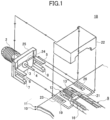
- Fig. 1 is an exploded view of a configuration 18 of mounting a coaxial RF connector 25 of the edge mount, end launch to a substrate 10 disclosed in a patent document No. 1.
- the connector 25 has a base plate 3 through which a threaded end 2 protrudes, and the end 2 is formed to receive a corresponding male SMA connector.
- a central conductor 4, and four mounting protrusions 5, 6, 7, and 8 extend from the base plate 3.
- a quasi-coaxial transmission line 9 formed on the substrate 10 has a strip of metal 13 formed on a top face of a dielectric material layer 12, and a metal layer 16 covering the dielectric material layer 12 and the strip of metal 13.
- the quasi-coaxial transmission line 9 extends to a position near an end of the substrate 10 (stops short of the end) to avoid an unintended connection between the strip of metal 13 and the base plate 3.
- the strip of metal 13 is exposed because the metal layer 16 is disposed not from the end of the substrate 10.
- Patent Document 1 Japanese Laid-open Patent Application No. 2003-208950 .
- US2017352937 describes a method to design and assemble a connector for the transition between a coaxial cable and a microstrip line, particularly for the one that features the attenuation or even elimination of a resonant response caused by the excitation of the first higher-order mode of the conventional coaxial connector from the frequency response of the transition.
- US4737111 describes a means for connecting an electroconductive circuit mounted on a printed circuit board to an outside circuit in such a manner that an operator can test fully and align the electroconductive circuit mounted on the printed circuit board prior to the final assembly of the printed circuit board within a circuit box wherein the printed circuit board is installed for operation.
- JPS5586204 describes an adaptor to connect a coaxial cable to microstrip lines.
- CZ2010833 describes an adaptor for connecting a coaxial line with a planar line carried on a substrate with a ground plane wherein the adapter consists of a coaxial connector with an internal conductor connecting the coaxial line with the planar line through a face with a through-hole of constant diameter.
- the prior art technology uses the shielding cover, which is a separate part with respect to the coaxial connector, to shield portions between the substrate and the coaxial connector, making it difficult to make the electric potentials of the base plate and the shielding cover of the coaxial connector to be identical. As a result, propagation characteristics of a signal between the substrate and the coaxial connector may be degraded.
- a coaxial connector and a substrate with a coaxial connector capable of avoiding a degradation of propagation characteristics of a signal can be provided.
- Figs. 2-7 and 9 relate to coaxial connectors that do not have all the features defined in independent claim 1. Nevertheless, said coaxial connectors are considered useful for understanding the present invention.
- a X-axis direction, a Y-axis direction, and a Z-axis direction denote a direction parallel to an X-axis, a direction parallel to a Y-axis, and a direction parallel to a Z-axis, respectively.
- the X-axis direction, the Y-axis direction, and the Z-axis direction are orthogonal to each other.
- An XY-plane, a YZ-plane, and a ZX-plane denote a virtual plane parallel to the X-axis direction and the Y-axis direction, a virtual plane parallel to the Y-axis direction and the Z-axis direction, and a virtual plane parallel to the Z-axis direction and the X-axis direction, respectively.
- a coaxial connector and a substrate with a coaxial connector are used to propagate a signal in a high frequency band (e.g., 0.3-300 GHz), e.g., microwaves or millimeter waves.
- a high frequency band includes a 0.3-3 GHz UHF band, a 3-30 GHz SHF band, and a 30-300 GHz EHF band.
- Examples of a high-frequency device formed on a substrate with a coaxial connector according to each of the present embodiments include a planar antenna, a planar waveguide (a planar transmission line), and the like.
- Fig. 2 is a partially magnified plan view depicting a substrate with a coaxial connector in one comparative example.
- Fig. 3 is a partial cross-sectional view of the substrate with the coaxial connector in the comparative example.
- Figs. 2 and 3 depict a configuration in which a coaxial connector 151 is attached to an edge of a substrate 101.
- the substrate 101 includes a plate-like dielectric layer 140, a power supply line 130 provided on one side of the dielectric layer 140, and a ground conductor 120 opposing the power supply line 130 via the dielectric layer 140.
- a transmission line 160 is formed on the substrate 101.
- the transmission line 160 is a microstrip line having a structure that includes the dielectric layer 140, the power supply line 130 formed on a first principal surface 141 of the dielectric layer 140, and the ground conductor 120 formed on a second principal surface 142 of the dielectric layer 140.
- the power supply line 130 is a planar conductor pattern whose surface is parallel to an XY plane and is formed on the first principal surface 141.
- the ground conductor 120 is a conductor pattern whose surface is parallel to the XY plane and is a conductor pattern formed on the second principal surface 142.
- the coaxial connector 151 includes a base 153, a coaxial structure 156 provided in the base 153, and a pair of protrusions 157 projecting from the base 153.
- the coaxial structure 156 has a configuration in which the dielectric 155 is between a central conductor 154 and an outer conductor 150.
- One end of the coaxial structure 156 is provided with a connecting section 152 to which an end of a coaxial cable, not depicted, is connected.
- the central conductor 154 has a contact portion 154a that extends from the other end opposite to the connecting section 152.
- the contact portion 154a is in contact with the power supply line 130 formed on the first principal surface 141 of the substrate 101 that is inserted toward the base 153 between the contact portion 154a and the pair of protrusions 157.
- the pair of protrusions 157 protrude from the X-axis ends of the base 153 toward the substrate 101, i.e., in the direction opposite to the Y-axis direction.
- the coaxial connector 151 is attached to the substrate 101 with the contact portion 154a conductively in contact with the power supply line 130. This way of attaching the coaxial connector 151 to the substrate 101 allows for transmission of a high frequency signal between the transmission line 160 formed on the substrate 101 and a coaxial cable not depicted whose one end is connected to the connecting section 152 of the coaxial connector 151.
- an outer edge portion 159 located at an edge of the substrate 101 may often have slopes 143 and 144 formed by chamfering.
- the slope 143 is a portion of the outer edge portion 159 at which the first principal surface 141 side is chamfered, and the power supply line 130 is not formed.
- the slope 144 is a portion of the outer edge portion 159 at which the second principal surface 142 side is chamfered, and the ground conductor 120 is not formed.
- Fig. 4 is a diagram illustrating a characteristic impedance of a signal path of a substrate with a coaxial connector in the comparative example.
- a characteristic impedance of the transmission line 160 formed on the substrate 101, a characteristic impedance of the coaxial connector 151, and a characteristic impedance of a coaxial cable connected to the coaxial connector 151 is 50 ⁇ .
- at least the contact portion 154a is not shielded, and also, an impedance section Z2 having a characteristic impedance different from 50 ⁇ is generated between the transmission line 160 and the coaxial connector 151.
- the impedance section Z2 where the characteristic impedance is discontinuous is present between the substrate 101 and the coaxial connector 151, multiple reflections of a signal that is transmitted may occur, resulting in degradation in the propagation characteristics of the signal (e.g., an increase in the transmission loss).
- a coaxial connector and a substrate with a coaxial connector have configurations that can avoid degradation in the signal propagation characteristics between the substrate and the coaxial connector.
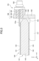
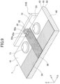
- Fig. 5 is a partial magnified perspective view depicting a coaxial connector and a substrate with the coaxial connector according to a first embodiment.
- Fig. 6 is a partially magnified plan view depicting the substrate with the coaxial connector according to the first embodiment.
- Fig. 7 is a partial cross-sectional view of the substrate with the coaxial connector according to the first embodiment.
- Figs. 5-7 depict a configuration in which the coaxial connector 51A is attached to an edge of the substrate 1.
- the substrate 1 includes a plate-like dielectric layer 40, a power supply line 30 provided on one side of the dielectric layer 40, and a ground conductor 20 opposite to the power supply line 30 via the dielectric layer 40.
- a transmission line 60 is formed in the substrate 1.
- the transmission line 60 is a microstrip line having a structure including the dielectric layer 40, the power supply line 30 formed on a first principal surface 41 of the dielectric layer 40, and the ground conductor 20 formed on a second principal surface 42 of the dielectric layer 40.
- the dielectric layer 40 has the first principal surface 41 and the second principal surface 42 opposite to the first principal surface 41.
- Figs. 5 and 6 depict the power supply line 30 provided on the first principal surface 41 side of the dielectric layer 40.
- Fig. 7 depicts the ground conductor 20 disposed on the second principal surface 42 side of the dielectric layer 40.
- the first principal surface 41 is an example of a first surface of the dielectric layer.
- the second principal surface 42 is an example of a second surface opposite the first surface of the dielectric layer.
- the dielectric layer 40 is a plate-like or sheet-like substrate mainly containing dielectric. Both the first principal surface 41 and the second principal surface 42 are parallel to the XY plane.
- the dielectric layer 40 may be, for example, a dielectric substrate or a dielectric sheet.
- a material of the dielectric layer 40 include, but are not limited to, glasses such as quartz glass, soda-lime glass, alkalifree glass, aluminosilicate glass, borosilicate glass, alkaline borosilicate glass, and the like, ceramics, fluororesins such as polytetrafluoroethylene, liquid crystal polymers, cycloolefin polymers, polycarbonates, and the like.
- the material of the dielectric layer 40 may be a transparent dielectric member through which visible light is transmitted, for example, to improve designability.
- a translucent dielectric member may be used instead of the transparent dielectric member. Transmittance with respect to visible light of the dielectric layer 40 is preferably greater than or equal to 30%, more preferably greater than or equal to 50%, yet more preferably greater than or equal to 70%, especially preferably greater than or equal to 80%, and most preferably greater than or equal to 90%, in order to avoid blockage of visible light.
- the power supply line 30 is a planar conductor pattern whose surface is parallel to the XY plane.
- the power supply line 30 is a conductor pattern formed on the first principal surface 41 and may be formed of a conductor sheet or a conductor substrate disposed on the first principal surface 41. Examples of the material of the conductor used in the power supply line 30 include, but are not limited to, gold, silver, copper, platinum, aluminum, chromium, and the like.
- the power supply line 30 is an example of a signal line in contact with the dielectric layer 40. For example, in the case where the transmission line 60 is a microstrip line, the power supply line 30 corresponds to a strip conductor.
- the power supply line 30 may be formed on the first principal surface 41 side via an interlayer such as polyvinyl butyral or ethylene vinyl acetate, or an adhesive layer such as an optically clear adhesive (OCA).
- OCA optically clear adhesive
- the power supply line 30 may be also in direct contact with the first principal surface 41.
- the power supply line 30 is a solid pattern of an area that has transmittance with respect to visible light lower than transmittance with respect to visible light of the dielectric layer 40.
- the entire power supply line 30 is made of an opaque planar conductor.
- the ground conductor 20 is a pattern of a conductor whose surface is parallel to the XY plane.
- the ground conductor 20 is a conductor pattern formed on the second principal surface 42 side and may be formed of a conductor sheet or a conductor substrate disposed on the second principal surface 42 side. Examples of the material of the ground conductor 20 include, but are not limited to, gold, silver, copper, platinum, aluminum, chromium, and the like.
- the ground conductor 20 is in contact with the dielectric layer 40.
- the ground conductor 20 may be formed on the second principal surface 42 side via an interlayer such as polyvinyl butyral or ethylene vinyl acetate, or an adhesive layer such as an optically clear adhesive (OCA).
- OCA optically clear adhesive
- the ground conductor 20 may be also in direct contact with the second principal surface 42.
- the ground conductor 20 is a solid pattern of an area that has transmittance with respect to visible light lower than the transmission with respect to visible light of the dielectric layer 40.
- the entire ground conductor 20 is made of an opaque planar conductor.
- the ground conductor 20 may be a pattern of a conductor having a mesh shape such that thus-formed lattice-like apertures improve designability.
- the mesh structure improves transmittance with respect to visible light and allows both designability and conductivity to be achieved.
- the ground conductor 20 may be the same as or differ from the dielectric layer 40 in transmittance with respect to visible light.
- the coaxial connector 51A includes a base 53, a coaxial structure 56 provided in the base 53, and a protrusion 57 protruding from a base surface 53a of the base 53.
- the base 53 has the base surface 53a parallel to the ZX plane.
- the base surface 53a is a portion facing an end surface 45 of the substrate 1.
- the end surface 45 is a portion in the Y-axis direction, which is perpendicular to the direction normal to the substrate 1 (in this case, the Z-axis direction).
- the contact portion 54a protrudes from the base surface 53a of the base 53.
- the expression that "the contact portion 54a protrudes from the base surface 53a” means that the contact portion 54a protrudes toward the substrate 1 with respect to a ZX plane including the base surface 53a.
- the base surface 53a is coplanar with one end surface of the dielectric 55 included in the coaxial structure 56.
- the base surface 53a may be at a position shifted along the Y-axis direction or the direction opposite thereto with respect to the end surface of the dielectric 55.
- the contact portion 54a When the substrate 1 is inserted between the contact portion 54a and the protrusion 57 toward the base surface 53a, the contact portion 54a is electrically in contact with the power supply line 30 formed on the first principal surface 41 of the inserted substrate 1 at a power supply end 33. It is preferable that the contact portion 54a and the power supply line 30 be electrically connected through a conductive connection implemented by a conductive adhesive, a solder, or the like.
- the protrusion 57 is a conductor having the same electrical potential as the outer conductor 50 of the coaxial structure 56, for example. Accordingly, when the substrate 1 is inserted between the contact portion 54a and the protrusion 57 toward the base surface 53a, the ground conductor 20 in contact with the protrusion 57 can have the same electrical potential as the electrical potential of the outer conductor 50.
- the protrusion 57 may be a member integrally formed with the base 53 or a separate member connected to the base 53.
- the protrusion 57 may, for example, be a portion that supports, from the lower side (from the lower side with respect to the Z-axis direction), the substrate 1 inserted between the contact portion 54a and the protrusion 57 toward the base surface 53a.
- the protrusion 57 is a part of an attaching structure for attaching the coaxial connector 51A to an edge of substrate 1.
- the coaxial connector 51A is attached to the substrate 1 with the contact portion 54a electrically conductively in contact with the power supply line 30.
- a high frequency signal can be transmitted between the transmission line 60 formed in the substrate 1 and a coaxial cable (not depicted) whose one end is connected to the connecting section 52 of the coaxial connector 51A.
- an outer edge portion 59 located at an edge of the substrate 1 often has slopes 43 and 44 formed by chamfering.
- the first slope 43 is a portion of the outer edge portion 59, in which the first principal surface 41 side is chamfered, and the power supply line 30 is not formed.
- the second slope 44 is a portion of the outer edge portion 59, in which the second principal surface 42 is chamfered, and the ground conductor 20 is not formed.
- the outer conductor 50 in the first embodiment has a protruding conductor 50a that protrudes from the base surface 53a and is not in contact with the substrate 1 inserted between the contact portion 54a and the protrusion 57.
- the expression "the protruding conductor 50a that protrudes from the base surface 53a” means that the protruding conductor 50a protrudes toward the substrate 1 with respect to a ZX plane including the base surface 53a. In the first embodiment, there is a space along the direction normal to the substrate 1 between the protruding conductor 50a and the slope 43.
- the protruding conductor 50a By thus providing the protruding conductor 50a, at least the contact portion 54a can be shielded by the protruding conductor 50a. Therefore, discontinuity of characteristic impedance occurring due to the outer edge portion 59 between the transmission line 60 and the coaxial connector 51A is reduced, and it is possible to avoid degradation in the propagation characteristics of a signal between the substrate 1 and the coaxial connector 51A. For example, multiple reflection of a signal transmitted between the substrate 1 and the coaxial connector 51A comes to be not likely to occur, and an increase in transmission loss can be avoided.
- the protruding conductor 50a protrudes from the base surface 53a in such a manner that the contact portion 54a is positioned between the substrate 1, inserted between the contact portion 54a and the protrusion 57, and the protruding conductor 50a protruding from the base surface 53a.
- the protruding conductor 50a is an eave-like portion extending from the coaxial structure 56 in a direction parallel to an axial direction of the coaxial structure 56 and has the same electric potential as the electric potential of the outer conductor 50.
- the protruding conductor 50a When viewed in a direction normal to the substrate 1 with the substrate 1 inserted between the contact portion 54a and the protrusion 57, the protruding conductor 50a preferably protrudes from the base surface 53a in such a manner that the protruding conductor 50a overlaps the outer edge portion 59. Thereby, it is possible to further reduce discontinuity of characteristic impedance, occurring due to the outer edge portion 59, between the transmission line 60 and the coaxial connector 51A, and it is possible to further avoid degradation in the propagation characteristics of a signal between the substrate 1 and the coaxial connector 51A.
- the protruding conductor 50a may protrude from the base surface 53a as far as a boundary between the power supply line 30 (power supply end 33) and the outer edge portion 59, or may protrude beyond the boundary, when viewed from a direction normal to the substrate 1. Protruding of the protruding conductor 50a from the base surface 53a up to or beyond the boundary reduces discontinuity of characteristic impedance, occurring due to the outer edge portions 59, between the transmission line 60 and the coaxial connector 51A, as compared to protruding of the protruding conductor 50a from the base surface 53a stopping short of the boundary. Thus, degradation in the propagation characteristics of a signal between the substrate 1 and the coaxial connector 51A can be further avoided.
- the protrusion 57 protrudes from the base surface 53a in such a manner that the protrusion 57 overlaps the contact portion 54a.
- the protrusion 57 may protrude from the base surface 53a as far as a distal end of the contact portion 54a or protrude beyond the distal end of the contact portion 54a, when viewed from a direction normal to the substrate 1.
- the protrusion 57 protruding from the base surface 53a up to or beyond the distal end can reduce discontinuity of the characteristic impedance, occurring due to the outer edge portion 59, between the transmission line 60 and the coaxial connector 51A, compared to protruding of the protrusion 57 from the base surface 53a stopping short of the distal end.
- degradation in the propagation characteristics of a signal between the substrate 1 and the coaxial connector 51A can be further avoided.
- parallelism of the end surface 45 in relation to the base surface 53a is preferably 100 ⁇ m or less, and more preferably 50 ⁇ m or less, from the point of view of restricting a drop in propagation characteristics of signals between the substrate 1 and the coaxial connector 51A.
- a calculated average roughness Ra of the end surface 45 is preferably 3.2 ⁇ m or less, and more preferably 1.6 ⁇ m or less, from the point of view of restricting a drop in propagation characteristics of the signals between the substrate 1 and the coaxial connector 51A. This is to enable highly accurate management of a length dimension of a part of the contact portion 54a which is not in contact with the power supply line 30 in a state of contact between the end surface 45 and the base surface 53a.
- the calculated average roughness Ra is a value defined by JIS B 0601:2001.
- an impedance adjusting portion 34 for implementing impedance matching may be provided at a portion of (at a location pathway along) the transmission line 60 such as a microstrip line.
- Fig. 5 depicts an example in which the impedance adjusting portion 34 is separated from the slope 43
- Fig. 6 depicts an example in which the impedance adjusting portion 34 is in contact with the slope 43.
- the impedance adjusting portion 34 By providing the impedance adjusting portion 34 at a portion of the transmission line 60, the advantageous effects of reducing discontinuity in characteristic impedance occurring due to the outer edge portion 59 between the transmission line 60 and the coaxial connector 51A are improved than a case where the impedance adjusting portion 34 is not provided. Therefore, it is possible to further avoid degradation in the propagation characteristics of a signal between the substrate 1 and the coaxial connector 51A.
- the impedance adjusting portion 34 may be implemented by stubs branching from the power supply line 30 on the first principal surface 41 of the substrate 1.
- the stubs are distribution-element circuits connected at locations pathway along the transmission line 60. Patterns of the stubs are formed, for example, in the same manner as a pattern of the power supply line 30.
- by forming the stubs laterally symmetrical with respect to the longitudinal direction of the power supply line 30, for example influences of the stubs on directivity of an antenna conductor, not depicted, connected at the distal ends of the transmission line 60, can be reduced.
- the impedance adjusting portion 34 may include a matching circuit formed of a lumped-element circuit using a reactance element such as an inductor or a capacitor.
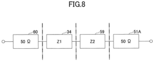
- Fig. 8 is a diagram illustrating characteristic impedances of signal paths with respect to the substrate with the coaxial connector according to the first embodiment.
- characteristic impedance of the transmission line 60 formed on the substrate 1 characteristic impedance of the coaxial connector 51A, and characteristic impedance of a coaxial cable connected to the coaxial connector 51A is 50 ⁇ .
- an impedance section Z1 can be formed between the transmission line 60 and the outer edge portion 59.
- the impedance section Z1 being thus formed compensates for a change in characteristic impedance caused by the outer edge portion 59. Therefore, it is possible to reduce discontinuity of characteristic impedance between the transmission line 60 and the coaxial connector 51A, and avoid degradation in the propagation characteristics of a signal between the substrate 1 and the coaxial connector 51A.
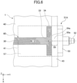
- Fig. 9 is a partially magnified perspective view depicting a coaxial connector and a substrate with the coaxial connector view according to a second embodiment.
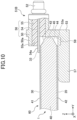
- Fig. 10 is a partial cross-sectional view of the substrate with the coaxial connector according to the second embodiment.
- Figs. 9 and 10 depict a configuration in which the coaxial connector 51B is attached to an edge of the substrate 1.
- a protruding dielectric 55a is added to the first embodiment.
- a dielectric 55 in the second embodiment has the protruding dielectric 55a protruding from a base surface 53a toward between a contact portion 54a and a protruding conductor 50a.
- the expression "the protruding dielectric 55a protruding from a base surface 53a” means that the protruding dielectric 55a protrudes toward the substrate 1 with respect to a ZX plane including the base surface 53a.
- the protruding dielectric 55a may protrude from the base surface 53a as far as a boundary between a power supply line 30 (power supply end 33) and the outer edge portion 59, or may protrude beyond the boundary, when viewed from a direction normal to the substrate 1.
- the protruding dielectric 55a protrudes from the base surface 53a to or beyond the boundary to reduce discontinuity of characteristic impedance occurring due to the outer edge portions 59 between the transmission line 60 and the coaxial connector 51B as compared to a configuration in which the protruding dielectric 55a protruding from the base surface 53a stops short of the boundary. That is, degradation in the propagation characteristics of a signal between the substrate 1 and the coaxial connector 51B can be more surely avoided.
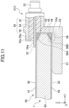
- Fig. 11 is a partial cross-sectional view of a coaxial connector and a substrate with the coaxial connector according to a third embodiment.
- Fig. 11 depicts a configuration in which the coaxial connector 51C is attached to an edge of the substrate 1.
- the third embodiment adds dielectric members 58A and 58B to the second embodiment.
- the dielectric member 58A is a generally triangular prismatic element having a side along a slope 43, a side along a contact portion 54a, and a side along a base surface 53a. At least a portion of a space between the contact portion 54a and the slope 43 is filled with the dielectric member 58A.
- the dielectric member 58B is a generally triangular prismatic element having a side along a slope 44, a side along a protrusion 57, and a side along the base surface 53a. At least a portion of a space between the protrusion 57 and the slope 44 is filled with the dielectric member 58B.
- dielectric members 58A and 58B By providing the dielectric members 58A and 58B, discontinuity of characteristic impedance occurring due to an outer edge portion 59 between a transmission line 60 and the coaxial connector 51C is reduced, and degradation in the propagation characteristics of a signal between the substrate 1 and the coaxial connector 51C is avoided. For example, multiple reflection of a signal transmitted between the substrate 1 and the coaxial connector 51C comes to be not likely to occur, and an increase in transmission loss is avoided.
- a material of the dielectric member 58A may be similar to or have a higher dielectric constant than a dielectric constant of a dielectric layer 40.
- Specific examples include, but are not limited to, glasses such as quartz glass, soda-lime glass, alkalifree glass, aluminosilicate glass, borosilicate glass, alkali borosilicate glass, and the like, ceramics, fluororesins such as polytetrafluoroethylene, liquid crystal polymers, cycloolefin polymers, polycarbonates, and the like.
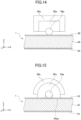
- Figs. 12-15 depict examples of configurations of protruding conductors and protruding dielectrics. Any of the configurations of Figs. 12-15 are applicable to each of the embodiments described above.
- Each of the protruding conductor 50a and the protruding dielectric 55a depicted in each of Figs. 12-15 protrudes from the base surface 53a to surround a portion of the outer peripheral surface of the contact portion 54a.
- each of the protruding conductor 50a and the protruding dielectric 55a has an eave shape obtained from a circular cylinder being approximately halved.
- the protruding conductor 50a has an eave shape obtained from a square or rectangular cylinder being approximately halved
- the protruding dielectric 55a has an eave shape obtained from a circular cylinder being approximately halved.
- each of the protruding conductor 50a and the protruding dielectric 55a has an eave shape obtained from a square or rectangular cylinder being approximately halved.
- a transmission line formed on a substrate is not limited to a microstrip line, and may be another transmission line, such as a coplanar line or a coplanar line with a ground.
Landscapes
- Engineering & Computer Science (AREA)
- Microelectronics & Electronic Packaging (AREA)
- Manufacturing & Machinery (AREA)
- Coupling Device And Connection With Printed Circuit (AREA)
- Details Of Connecting Devices For Male And Female Coupling (AREA)
Applications Claiming Priority (2)
| Application Number | Priority Date | Filing Date | Title |
|---|---|---|---|
| JP2018208766 | 2018-11-06 | ||
| PCT/JP2019/042530 WO2020095783A1 (ja) | 2018-11-06 | 2019-10-30 | 同軸コネクタ及び同軸コネクタ付き基板 |
Publications (3)
| Publication Number | Publication Date |
|---|---|
| EP3879640A1 EP3879640A1 (en) | 2021-09-15 |
| EP3879640A4 EP3879640A4 (en) | 2022-08-03 |
| EP3879640B1 true EP3879640B1 (en) | 2025-04-09 |
Family
ID=70612223
Family Applications (1)
| Application Number | Title | Priority Date | Filing Date |
|---|---|---|---|
| EP19882315.5A Active EP3879640B1 (en) | 2018-11-06 | 2019-10-30 | Coaxial connector and substrate equipped with coaxial connector |
Country Status (10)
| Country | Link |
|---|---|
| US (1) | US11967792B2 (pl) |
| EP (1) | EP3879640B1 (pl) |
| JP (1) | JPWO2020095783A1 (pl) |
| KR (1) | KR20210087933A (pl) |
| CN (1) | CN112913088A (pl) |
| DK (1) | DK3879640T3 (pl) |
| ES (1) | ES3035202T3 (pl) |
| FI (1) | FI3879640T3 (pl) |
| PL (1) | PL3879640T3 (pl) |
| WO (1) | WO2020095783A1 (pl) |
Families Citing this family (4)
| Publication number | Priority date | Publication date | Assignee | Title |
|---|---|---|---|---|
| WO2022050917A1 (en) * | 2020-09-01 | 2022-03-10 | Aselsan Elektroni̇k Sanayi̇ Ve Ti̇caret Anoni̇m Şi̇rketi̇ | Soldered adapter modulation structure |
| JP7565341B2 (ja) * | 2020-10-12 | 2024-10-10 | オリンパス株式会社 | 導波管の接続構造、導波管コネクタ、導波管ユニット、モード変換機、撮像装置、及び、内視鏡 |
| JP7488242B2 (ja) * | 2021-11-16 | 2024-05-21 | 矢崎総業株式会社 | アンテナケーブルのノイズ抑制構造 |
| KR102745032B1 (ko) * | 2022-08-31 | 2024-12-23 | (주)니나노 | Rf 커넥터 |
Family Cites Families (24)
| Publication number | Priority date | Publication date | Assignee | Title |
|---|---|---|---|---|
| JPS5586204A (en) * | 1978-12-23 | 1980-06-28 | Fujitsu Ltd | Microstrip coaxial converter |
| JPS5830761B2 (ja) * | 1979-07-27 | 1983-07-01 | 株式会社トキメック | 同軸−マイクロストリツプ変換器 |
| US4737111A (en) * | 1985-11-19 | 1988-04-12 | C-Cor Electronics, Inc. | RF connector for use in testing a printed circuit board |
| JPS63316901A (ja) * | 1987-06-19 | 1988-12-26 | Mitsubishi Electric Corp | 同軸コネクタ |
| US5404117A (en) * | 1993-10-01 | 1995-04-04 | Hewlett-Packard Company | Connector for strip-type transmission line to coaxial cable |
| US6457979B1 (en) | 2001-10-29 | 2002-10-01 | Agilent Technologies, Inc. | Shielded attachment of coaxial RF connector to thick film integrally shielded transmission line on a substrate |
| US6957980B2 (en) * | 2003-05-02 | 2005-10-25 | Insert Enterprise Co., Ltd. | Insert type super mini microwave connector |
| US6894590B2 (en) * | 2003-05-30 | 2005-05-17 | Agilent Technologies, Inc. | Apparatus and method to introduce signals into a shielded RF circuit |
| JP2005236648A (ja) * | 2004-02-19 | 2005-09-02 | Mitsubishi Electric Corp | 同軸マイクロストリップ線路変換器 |
| US7344381B2 (en) * | 2004-04-29 | 2008-03-18 | Emerson Network Power Connectivity Solutions, Inc. | High frequency edge mount connector |
| JP2007141607A (ja) * | 2005-11-17 | 2007-06-07 | Yazaki Corp | 同軸コネクタの基板接続構造 |
| JP2009099283A (ja) * | 2007-10-12 | 2009-05-07 | Murata Mfg Co Ltd | 高周波同軸コネクタ、これを用いた高周波同軸コネクタの実装構造及び高周波同軸コネクタの接続方法 |
| US8035466B2 (en) * | 2009-01-12 | 2011-10-11 | Kenneth Ray Payne | High frequency electrical connector |
| US7713067B1 (en) * | 2009-03-03 | 2010-05-11 | Bomar Interconnect Products, Inc. | Connector with a conductive shell with an extension to stradle a circuit board |
| US7946854B2 (en) * | 2009-07-21 | 2011-05-24 | Tyco Electronics Corporation | Electrical connector assembly having shield member |
| JP5240726B2 (ja) * | 2009-10-28 | 2013-07-17 | 京セラ株式会社 | 半導体装置と回路基板との接続構造 |
| US8384492B2 (en) * | 2010-09-07 | 2013-02-26 | National Taipei University Of Technology | Coaxial line to microstrip connector having slots in the microstrip line for receiving an encircling metallic plate |
| CZ303925B6 (cs) * | 2010-11-12 | 2013-06-26 | Ceské vysoké ucení technické v Praze Fakulta elektrotechnická | Adaptér pro propojení koaxiálního vedení s planárním vedením, zejména pro mericí prístroje |
| FR2985157B1 (fr) * | 2011-12-23 | 2014-10-10 | Thales Sa | Dispositif de protection electromagnetique apte a proteger une liaison hyperfrequences entre un connecteur et un element hyperfrequences |
| JP6103898B2 (ja) * | 2012-11-28 | 2017-03-29 | 三菱電機株式会社 | 同軸コネクタおよびその基板接続構造 |
| CN204271230U (zh) * | 2014-12-17 | 2015-04-15 | 电子科技大学 | 一种改善高频及驻波特性的sma接头到微带过渡装置 |
| TWI563718B (en) * | 2015-06-11 | 2016-12-21 | Univ Nat Taipei Technology | Vertical Transition Structure |
| TWI560956B (en) * | 2016-06-07 | 2016-12-01 | Univ Nat Taipei Technology | Method to design and assemble a connector for the transition between a coaxial cable and a microstrip line |
| JP6853655B2 (ja) * | 2016-11-14 | 2021-03-31 | ヒロセ電機株式会社 | 基板とコネクタとの接続構造および基板 |
-
2019
- 2019-10-30 FI FIEP19882315.5T patent/FI3879640T3/fi active
- 2019-10-30 JP JP2020555998A patent/JPWO2020095783A1/ja active Pending
- 2019-10-30 CN CN201980069266.2A patent/CN112913088A/zh active Pending
- 2019-10-30 EP EP19882315.5A patent/EP3879640B1/en active Active
- 2019-10-30 DK DK19882315.5T patent/DK3879640T3/da active
- 2019-10-30 ES ES19882315T patent/ES3035202T3/es active Active
- 2019-10-30 KR KR1020217011507A patent/KR20210087933A/ko not_active Withdrawn
- 2019-10-30 PL PL19882315.5T patent/PL3879640T3/pl unknown
- 2019-10-30 WO PCT/JP2019/042530 patent/WO2020095783A1/ja not_active Ceased
-
2021
- 2021-04-19 US US17/233,710 patent/US11967792B2/en active Active
Also Published As
| Publication number | Publication date |
|---|---|
| US20210242641A1 (en) | 2021-08-05 |
| DK3879640T3 (da) | 2025-07-21 |
| ES3035202T3 (en) | 2025-08-29 |
| EP3879640A4 (en) | 2022-08-03 |
| CN112913088A (zh) | 2021-06-04 |
| JPWO2020095783A1 (ja) | 2021-10-14 |
| WO2020095783A1 (ja) | 2020-05-14 |
| FI3879640T3 (fi) | 2025-07-04 |
| EP3879640A1 (en) | 2021-09-15 |
| PL3879640T3 (pl) | 2025-08-11 |
| KR20210087933A (ko) | 2021-07-13 |
| US11967792B2 (en) | 2024-04-23 |
Similar Documents
| Publication | Publication Date | Title |
|---|---|---|
| US11417938B2 (en) | Printed circuit board with substrate-integrated waveguide transition | |
| US11967792B2 (en) | Coaxial connector and substrate with coaxial connector | |
| CN100367417C (zh) | 扁平电缆、扁平电缆片、以及扁平电缆片的制造方法 | |
| US11224120B2 (en) | Print circuit board, optical module, and optical transmission equipment | |
| KR102687557B1 (ko) | 안테나 어셈블리 및 전자 장치 | |
| WO2009044987A1 (en) | Ultra wideband hermetically sealed surface mount technology for microwave monolithic integrated circuit package | |
| US20110234473A1 (en) | Cable connector and antenna component | |
| US10992015B2 (en) | Coupling comprising a guide member embedded within a blind via of a post-wall waveguide and extending into a hollow tube waveguide | |
| US6624722B2 (en) | Coplanar directional coupler for hybrid geometry | |
| US11011814B2 (en) | Coupling comprising a conductive wire embedded in a post-wall waveguide and extending into a hollow tube waveguide | |
| US20250096481A1 (en) | Transmission device and antenna | |
| KR101182425B1 (ko) | 스터브가 있는 슬롯 안테나 | |
| US12237590B2 (en) | Printed circuit board integrated antenna for transmitting / receiving data | |
| US11909133B2 (en) | Dielectrically loaded printed dipole antenna | |
| EP3996201B1 (en) | Coaxial microstrip line conversion circuit | |
| US20250226582A1 (en) | Antenna module | |
| JP3895716B2 (ja) | 高周波伝送基板および高周波伝送基板接続構造 | |
| SE2130275A1 (en) | A circuit board-to-waveguide transition with an h-plane-fed patch antenna | |
| KR20240018896A (ko) | 표면 실장형 고주파수용 동축 커넥터 | |
| WO2024065281A1 (zh) | 一种缝隙天线及电子设备 | |
| CN117154408A (zh) | 毫米波天线组件以及显示装置 |
Legal Events
| Date | Code | Title | Description |
|---|---|---|---|
| STAA | Information on the status of an ep patent application or granted ep patent |
Free format text: STATUS: THE INTERNATIONAL PUBLICATION HAS BEEN MADE |
|
| PUAI | Public reference made under article 153(3) epc to a published international application that has entered the european phase |
Free format text: ORIGINAL CODE: 0009012 |
|
| STAA | Information on the status of an ep patent application or granted ep patent |
Free format text: STATUS: REQUEST FOR EXAMINATION WAS MADE |
|
| 17P | Request for examination filed |
Effective date: 20210429 |
|
| AK | Designated contracting states |
Kind code of ref document: A1 Designated state(s): AL AT BE BG CH CY CZ DE DK EE ES FI FR GB GR HR HU IE IS IT LI LT LU LV MC MK MT NL NO PL PT RO RS SE SI SK SM TR |
|
| DAV | Request for validation of the european patent (deleted) | ||
| DAX | Request for extension of the european patent (deleted) | ||
| A4 | Supplementary search report drawn up and despatched |
Effective date: 20220630 |
|
| RIC1 | Information provided on ipc code assigned before grant |
Ipc: H01R 24/50 20110101ALN20220624BHEP Ipc: H05K 3/34 20060101ALI20220624BHEP Ipc: H05K 1/02 20060101ALI20220624BHEP Ipc: H01R 13/6474 20110101ALI20220624BHEP Ipc: H01R 24/44 20110101ALI20220624BHEP Ipc: H01P 5/08 20060101AFI20220624BHEP |
|
| REG | Reference to a national code |
Ref country code: DE Ref legal event code: R079 Ipc: H01P0005080000 Ref country code: DE Ref legal event code: R079 Ref document number: 602019068556 Country of ref document: DE Free format text: PREVIOUS MAIN CLASS: H01R0013646600 Ipc: H01P0005080000 |
|
| GRAP | Despatch of communication of intention to grant a patent |
Free format text: ORIGINAL CODE: EPIDOSNIGR1 |
|
| STAA | Information on the status of an ep patent application or granted ep patent |
Free format text: STATUS: GRANT OF PATENT IS INTENDED |
|
| RIC1 | Information provided on ipc code assigned before grant |
Ipc: H01R 24/50 20110101ALN20241031BHEP Ipc: H05K 3/34 20060101ALI20241031BHEP Ipc: H05K 1/02 20060101ALI20241031BHEP Ipc: H01R 24/44 20110101ALI20241031BHEP Ipc: H01R 13/6474 20110101ALI20241031BHEP Ipc: H01P 5/08 20060101AFI20241031BHEP |
|
| INTG | Intention to grant announced |
Effective date: 20241112 |
|
| GRAS | Grant fee paid |
Free format text: ORIGINAL CODE: EPIDOSNIGR3 |
|
| GRAA | (expected) grant |
Free format text: ORIGINAL CODE: 0009210 |
|
| STAA | Information on the status of an ep patent application or granted ep patent |
Free format text: STATUS: THE PATENT HAS BEEN GRANTED |
|
| AK | Designated contracting states |
Kind code of ref document: B1 Designated state(s): AL AT BE BG CH CY CZ DE DK EE ES FI FR GB GR HR HU IE IS IT LI LT LU LV MC MK MT NL NO PL PT RO RS SE SI SK SM TR |
|
| REG | Reference to a national code |
Ref country code: GB Ref legal event code: FG4D |
|
| REG | Reference to a national code |
Ref country code: CH Ref legal event code: EP |
|
| REG | Reference to a national code |
Ref country code: DE Ref legal event code: R096 Ref document number: 602019068556 Country of ref document: DE |
|
| REG | Reference to a national code |
Ref country code: IE Ref legal event code: FG4D |
|
| REG | Reference to a national code |
Ref country code: FI Ref legal event code: FGE |
|
| REG | Reference to a national code |
Ref country code: DK Ref legal event code: T3 Effective date: 20250715 |
|
| REG | Reference to a national code |
Ref country code: NL Ref legal event code: FP |
|
| REG | Reference to a national code |
Ref country code: SE Ref legal event code: TRGR |
|
| REG | Reference to a national code |
Ref country code: ES Ref legal event code: FG2A Ref document number: 3035202 Country of ref document: ES Kind code of ref document: T3 Effective date: 20250829 |
|
| REG | Reference to a national code |
Ref country code: AT Ref legal event code: MK05 Ref document number: 1784421 Country of ref document: AT Kind code of ref document: T Effective date: 20250409 |
|
| PG25 | Lapsed in a contracting state [announced via postgrant information from national office to epo] |
Ref country code: PT Free format text: LAPSE BECAUSE OF FAILURE TO SUBMIT A TRANSLATION OF THE DESCRIPTION OR TO PAY THE FEE WITHIN THE PRESCRIBED TIME-LIMIT Effective date: 20250811 |
|
| REG | Reference to a national code |
Ref country code: LT Ref legal event code: MG9D |
|
| PG25 | Lapsed in a contracting state [announced via postgrant information from national office to epo] |
Ref country code: GR Free format text: LAPSE BECAUSE OF FAILURE TO SUBMIT A TRANSLATION OF THE DESCRIPTION OR TO PAY THE FEE WITHIN THE PRESCRIBED TIME-LIMIT Effective date: 20250710 |
|
| PGFP | Annual fee paid to national office [announced via postgrant information from national office to epo] |
Ref country code: NL Payment date: 20250912 Year of fee payment: 7 Ref country code: PL Payment date: 20250912 Year of fee payment: 7 Ref country code: IT Payment date: 20250922 Year of fee payment: 7 |
|
| PG25 | Lapsed in a contracting state [announced via postgrant information from national office to epo] |
Ref country code: BG Free format text: LAPSE BECAUSE OF FAILURE TO SUBMIT A TRANSLATION OF THE DESCRIPTION OR TO PAY THE FEE WITHIN THE PRESCRIBED TIME-LIMIT Effective date: 20250409 |
|
| PGFP | Annual fee paid to national office [announced via postgrant information from national office to epo] |
Ref country code: BE Payment date: 20250917 Year of fee payment: 7 Ref country code: GB Payment date: 20250911 Year of fee payment: 7 |
|
| PG25 | Lapsed in a contracting state [announced via postgrant information from national office to epo] |
Ref country code: HR Free format text: LAPSE BECAUSE OF FAILURE TO SUBMIT A TRANSLATION OF THE DESCRIPTION OR TO PAY THE FEE WITHIN THE PRESCRIBED TIME-LIMIT Effective date: 20250409 |
|
| PG25 | Lapsed in a contracting state [announced via postgrant information from national office to epo] |
Ref country code: AT Free format text: LAPSE BECAUSE OF FAILURE TO SUBMIT A TRANSLATION OF THE DESCRIPTION OR TO PAY THE FEE WITHIN THE PRESCRIBED TIME-LIMIT Effective date: 20250409 |
|
| PGFP | Annual fee paid to national office [announced via postgrant information from national office to epo] |
Ref country code: FR Payment date: 20250908 Year of fee payment: 7 |
|
| PGFP | Annual fee paid to national office [announced via postgrant information from national office to epo] |
Ref country code: SE Payment date: 20250910 Year of fee payment: 7 |
|
| PG25 | Lapsed in a contracting state [announced via postgrant information from national office to epo] |
Ref country code: RS Free format text: LAPSE BECAUSE OF FAILURE TO SUBMIT A TRANSLATION OF THE DESCRIPTION OR TO PAY THE FEE WITHIN THE PRESCRIBED TIME-LIMIT Effective date: 20250709 |
|
| PG25 | Lapsed in a contracting state [announced via postgrant information from national office to epo] |
Ref country code: IS Free format text: LAPSE BECAUSE OF FAILURE TO SUBMIT A TRANSLATION OF THE DESCRIPTION OR TO PAY THE FEE WITHIN THE PRESCRIBED TIME-LIMIT Effective date: 20250809 |
|
| PG25 | Lapsed in a contracting state [announced via postgrant information from national office to epo] |
Ref country code: LV Free format text: LAPSE BECAUSE OF FAILURE TO SUBMIT A TRANSLATION OF THE DESCRIPTION OR TO PAY THE FEE WITHIN THE PRESCRIBED TIME-LIMIT Effective date: 20250409 |
|
| REG | Reference to a national code |
Ref country code: CH Ref legal event code: U11 Free format text: ST27 STATUS EVENT CODE: U-0-0-U10-U11 (AS PROVIDED BY THE NATIONAL OFFICE) Effective date: 20251101 |