EP3879584A1 - Light-emitting diode - Google Patents
Light-emitting diode Download PDFInfo
- Publication number
- EP3879584A1 EP3879584A1 EP19882208.2A EP19882208A EP3879584A1 EP 3879584 A1 EP3879584 A1 EP 3879584A1 EP 19882208 A EP19882208 A EP 19882208A EP 3879584 A1 EP3879584 A1 EP 3879584A1
- Authority
- EP
- European Patent Office
- Prior art keywords
- light emitting
- substrate
- light
- emitting device
- shielding layer
- Prior art date
- Legal status (The legal status is an assumption and is not a legal conclusion. Google has not performed a legal analysis and makes no representation as to the accuracy of the status listed.)
- Pending
Links
Images









Classifications
-
- H—ELECTRICITY
- H10—SEMICONDUCTOR DEVICES; ELECTRIC SOLID-STATE DEVICES NOT OTHERWISE PROVIDED FOR
- H10H—INORGANIC LIGHT-EMITTING SEMICONDUCTOR DEVICES HAVING POTENTIAL BARRIERS
- H10H20/00—Individual inorganic light-emitting semiconductor devices having potential barriers, e.g. light-emitting diodes [LED]
- H10H20/80—Constructional details
- H10H20/81—Bodies
- H10H20/819—Bodies characterised by their shape, e.g. curved or truncated substrates
- H10H20/82—Roughened surfaces, e.g. at the interface between epitaxial layers
-
- H—ELECTRICITY
- H10—SEMICONDUCTOR DEVICES; ELECTRIC SOLID-STATE DEVICES NOT OTHERWISE PROVIDED FOR
- H10H—INORGANIC LIGHT-EMITTING SEMICONDUCTOR DEVICES HAVING POTENTIAL BARRIERS
- H10H20/00—Individual inorganic light-emitting semiconductor devices having potential barriers, e.g. light-emitting diodes [LED]
- H10H20/80—Constructional details
- H10H20/81—Bodies
- H10H20/819—Bodies characterised by their shape, e.g. curved or truncated substrates
-
- H—ELECTRICITY
- H10—SEMICONDUCTOR DEVICES; ELECTRIC SOLID-STATE DEVICES NOT OTHERWISE PROVIDED FOR
- H10H—INORGANIC LIGHT-EMITTING SEMICONDUCTOR DEVICES HAVING POTENTIAL BARRIERS
- H10H20/00—Individual inorganic light-emitting semiconductor devices having potential barriers, e.g. light-emitting diodes [LED]
- H10H20/80—Constructional details
- H10H20/83—Electrodes
- H10H20/831—Electrodes characterised by their shape
- H10H20/8312—Electrodes characterised by their shape extending at least partially through the bodies
-
- H—ELECTRICITY
- H10—SEMICONDUCTOR DEVICES; ELECTRIC SOLID-STATE DEVICES NOT OTHERWISE PROVIDED FOR
- H10H—INORGANIC LIGHT-EMITTING SEMICONDUCTOR DEVICES HAVING POTENTIAL BARRIERS
- H10H20/00—Individual inorganic light-emitting semiconductor devices having potential barriers, e.g. light-emitting diodes [LED]
- H10H20/80—Constructional details
- H10H20/84—Coatings, e.g. passivation layers or antireflective coatings
-
- H—ELECTRICITY
- H10—SEMICONDUCTOR DEVICES; ELECTRIC SOLID-STATE DEVICES NOT OTHERWISE PROVIDED FOR
- H10H—INORGANIC LIGHT-EMITTING SEMICONDUCTOR DEVICES HAVING POTENTIAL BARRIERS
- H10H20/00—Individual inorganic light-emitting semiconductor devices having potential barriers, e.g. light-emitting diodes [LED]
- H10H20/80—Constructional details
- H10H20/85—Packages
- H10H20/855—Optical field-shaping means, e.g. lenses
-
- H—ELECTRICITY
- H10—SEMICONDUCTOR DEVICES; ELECTRIC SOLID-STATE DEVICES NOT OTHERWISE PROVIDED FOR
- H10H—INORGANIC LIGHT-EMITTING SEMICONDUCTOR DEVICES HAVING POTENTIAL BARRIERS
- H10H29/00—Integrated devices, or assemblies of multiple devices, comprising at least one light-emitting semiconductor element covered by group H10H20/00
- H10H29/10—Integrated devices comprising at least one light-emitting semiconductor component covered by group H10H20/00
- H10H29/14—Integrated devices comprising at least one light-emitting semiconductor component covered by group H10H20/00 comprising multiple light-emitting semiconductor components
- H10H29/142—Two-dimensional arrangements, e.g. asymmetric LED layout
-
- H—ELECTRICITY
- H10—SEMICONDUCTOR DEVICES; ELECTRIC SOLID-STATE DEVICES NOT OTHERWISE PROVIDED FOR
- H10H—INORGANIC LIGHT-EMITTING SEMICONDUCTOR DEVICES HAVING POTENTIAL BARRIERS
- H10H20/00—Individual inorganic light-emitting semiconductor devices having potential barriers, e.g. light-emitting diodes [LED]
- H10H20/01—Manufacture or treatment
- H10H20/011—Manufacture or treatment of bodies, e.g. forming semiconductor layers
- H10H20/013—Manufacture or treatment of bodies, e.g. forming semiconductor layers having light-emitting regions comprising only Group III-V materials
- H10H20/0133—Manufacture or treatment of bodies, e.g. forming semiconductor layers having light-emitting regions comprising only Group III-V materials with a substrate not being Group III-V materials
- H10H20/01335—Manufacture or treatment of bodies, e.g. forming semiconductor layers having light-emitting regions comprising only Group III-V materials with a substrate not being Group III-V materials the light-emitting regions comprising nitride materials
-
- H—ELECTRICITY
- H10—SEMICONDUCTOR DEVICES; ELECTRIC SOLID-STATE DEVICES NOT OTHERWISE PROVIDED FOR
- H10H—INORGANIC LIGHT-EMITTING SEMICONDUCTOR DEVICES HAVING POTENTIAL BARRIERS
- H10H20/00—Individual inorganic light-emitting semiconductor devices having potential barriers, e.g. light-emitting diodes [LED]
- H10H20/01—Manufacture or treatment
- H10H20/011—Manufacture or treatment of bodies, e.g. forming semiconductor layers
- H10H20/018—Bonding of wafers
-
- H—ELECTRICITY
- H10—SEMICONDUCTOR DEVICES; ELECTRIC SOLID-STATE DEVICES NOT OTHERWISE PROVIDED FOR
- H10H—INORGANIC LIGHT-EMITTING SEMICONDUCTOR DEVICES HAVING POTENTIAL BARRIERS
- H10H20/00—Individual inorganic light-emitting semiconductor devices having potential barriers, e.g. light-emitting diodes [LED]
- H10H20/01—Manufacture or treatment
- H10H20/032—Manufacture or treatment of electrodes
-
- H—ELECTRICITY
- H10—SEMICONDUCTOR DEVICES; ELECTRIC SOLID-STATE DEVICES NOT OTHERWISE PROVIDED FOR
- H10H—INORGANIC LIGHT-EMITTING SEMICONDUCTOR DEVICES HAVING POTENTIAL BARRIERS
- H10H20/00—Individual inorganic light-emitting semiconductor devices having potential barriers, e.g. light-emitting diodes [LED]
- H10H20/01—Manufacture or treatment
- H10H20/034—Manufacture or treatment of coatings
-
- H—ELECTRICITY
- H10—SEMICONDUCTOR DEVICES; ELECTRIC SOLID-STATE DEVICES NOT OTHERWISE PROVIDED FOR
- H10H—INORGANIC LIGHT-EMITTING SEMICONDUCTOR DEVICES HAVING POTENTIAL BARRIERS
- H10H20/00—Individual inorganic light-emitting semiconductor devices having potential barriers, e.g. light-emitting diodes [LED]
- H10H20/80—Constructional details
- H10H20/81—Bodies
- H10H20/811—Bodies having quantum effect structures or superlattices, e.g. tunnel junctions
- H10H20/812—Bodies having quantum effect structures or superlattices, e.g. tunnel junctions within the light-emitting regions, e.g. having quantum confinement structures
-
- H—ELECTRICITY
- H10—SEMICONDUCTOR DEVICES; ELECTRIC SOLID-STATE DEVICES NOT OTHERWISE PROVIDED FOR
- H10H—INORGANIC LIGHT-EMITTING SEMICONDUCTOR DEVICES HAVING POTENTIAL BARRIERS
- H10H20/00—Individual inorganic light-emitting semiconductor devices having potential barriers, e.g. light-emitting diodes [LED]
- H10H20/80—Constructional details
- H10H20/81—Bodies
- H10H20/822—Materials of the light-emitting regions
- H10H20/824—Materials of the light-emitting regions comprising only Group III-V materials, e.g. GaP
- H10H20/825—Materials of the light-emitting regions comprising only Group III-V materials, e.g. GaP containing nitrogen, e.g. GaN
-
- H—ELECTRICITY
- H10—SEMICONDUCTOR DEVICES; ELECTRIC SOLID-STATE DEVICES NOT OTHERWISE PROVIDED FOR
- H10H—INORGANIC LIGHT-EMITTING SEMICONDUCTOR DEVICES HAVING POTENTIAL BARRIERS
- H10H20/00—Individual inorganic light-emitting semiconductor devices having potential barriers, e.g. light-emitting diodes [LED]
- H10H20/80—Constructional details
- H10H20/83—Electrodes
- H10H20/832—Electrodes characterised by their material
- H10H20/833—Transparent materials
-
- H—ELECTRICITY
- H10—SEMICONDUCTOR DEVICES; ELECTRIC SOLID-STATE DEVICES NOT OTHERWISE PROVIDED FOR
- H10H—INORGANIC LIGHT-EMITTING SEMICONDUCTOR DEVICES HAVING POTENTIAL BARRIERS
- H10H20/00—Individual inorganic light-emitting semiconductor devices having potential barriers, e.g. light-emitting diodes [LED]
- H10H20/80—Constructional details
- H10H20/882—Scattering means
Definitions
- Exemplary embodiments of the invention relate generally to a light emitting device, and more specifically, to a light emitting device including a plurality of light emitting parts.
- Light emitting diodes as inorganic light sources, are being diversely used in various fields, such as display devices, vehicle lamps, and general lighting. Light emitting diodes are rapidly replacing existing light sources due to their longer lifetime, lower power consumption, and faster response speed than existing light sources.
- Devices constructed according to exemplary embodiments of the invention are capable of improving light efficiency and light extraction.
- a light emitting device includes a substrate having a first surface and a second surface opposing the first surface, a light emitting structure disposed on the first surface of the substrate and defining a light emitting area, and a first light shielding layer disposed on the second surface of the substrate and exposing at least a portion of the light emitting area, in which the second surface of the substrate has a rough surface that overlaps at least a portion the light emitting area.
- a thickness of a portion of the substrate including the rough surface may be less than a thickness of a portion of the substrate not formed with the rough surface.
- the second surface of the substrate may include a sidewall connected to the rough surface, and the first light shielding layer may extend to the sidewall of the substrate, at least partially cover the rough surface, and define a light extraction surface of the light emitting structure.
- the light extraction surface may have a width less than that of the rough surface and that of the light emitting area.
- the rough surface may include a convex and concave pattern, and a roughness of a portion of the convex and concave pattern formed in the light extraction surface may be different from that of a portion of the convex and concave pattern covered by the first light shielding layer.
- the first light shielding layer may have substantially the same width along the sidewall of the substrate.
- the sidewall of the substrate may be inclined with a predetermined slope, and the first light shielding layer may have a width that gradually decreases from the second surface of the substrate toward an inside of the substrate, and have a side surface vertically extending from the second surface of the substrate.
- the rough surface may be disposed within the light emitting area, and have a width less than the light emitting area.
- the rough surface may cover the light emitting area, and have a width equal to or greater than the light emitting area.
- the light emitting device may further include a second light shielding layer disposed on the first surface of the substrate and surrounding an outer side of the light emitting structure.
- the first surface of the substrate may have a convex part in the light emitting area and a concave part in an area excluding the light emitting area.
- the light emitting device may further include a second light shielding layer disposed in the concave part of the substrate and surrounding an outer side of the light emitting structure.
- a portion of the second light shielding layer disposed in the concave part and a portion of the first light shielding layer covering at least a portion of the rough surface of the substrate may overlap with each other.
- the rough surface may include a plurality of first holes, and at least a portion of the first holes may be disposed in the light emitting area.
- the first light shielding layer may be disposed in the first holes, extend along the second surface of the substrate to cover at least a portion of the light emitting area, and define a light extraction surface of the light emitting structure.
- the light extraction surface may have a width less than that of the light emitting area.
- the first holes formed in the light extraction surface may be filled with air.
- the first holes formed in the light extraction surface may be filled with the first light shielding layer.
- the light emitting device may further include a second light shielding layer disposed on the first surface of the substrate and surrounding an outer side of the light emitting structure.
- the first surface of the substrate may include a plurality of second holes, and the second light shielding layer may be disposed in at least a portion of the second holes.
- the light generated from a neighboring light emitting structure is prevented from being mixed, by first and second light shielding layers, it is possible to improve color reproducibility.
- the substrate since a substrate is formed to have a thin thickness only in a region where a rough surface is formed and retain a normal thickness in a remaining region, the substrate may support a plurality of light emitting structures and may not be damaged even by an external shock.
- the light generated by a light emitting structure is diffusively reflected by the rough surface, whereby light efficiency may be improved. Further, as the light shielding layer covers the ends of the rough surface, a light extraction surface may be defined, whereby the contrast of the light emitting device may be improved.
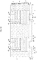
- FIGS. 1A and 1B are top views of a light emitting device according to an exemplary embodiment, and FIGS. 1C , 1D , and IE are cross-sectional views taken along line A-A' of FIG. 1A according to exemplary embodiments.
- FIG. 2A is a top view of a light emitting device according to another exemplary embodiment, and FIG. 2B is a cross-sectional view taken along line A-A' of FIG. 2A .
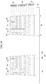
- FIG. 3A is a cross-sectional view of a light emitting structure according to an exemplary embodiment, and FIG. 3B is a cross-sectional view taken along lines A-A' and B-B' of FIG. 3A .
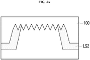
- FIGS. 4A , 4B , 5A , and 5B are cross-sectional views of the structures of rough surfaces and second light shielding layers according to exemplary embodiments.
- a light emitting device may include a substrate 100 and light emitting structures LED, each including a first light emitting part LE1, a second light emitting part LE2, and a third light emitting part LE3 stacked on the substrate 100.
- FIG. 1A is a plan view of the light emitting device when viewed from the third light emitting part LE3, and FIG. 1B is a plan view of the light emitting device when viewed from the substrate 100.
- FIG. 2A is a plan view of the light emitting device when viewed from the substrate 100.
- FIGS. 3A and 3B are enlarged views of a light emitting structure.
- the substrate 100 may be capable of growing a gallium nitride-based semiconductor layer thereon, and may include a sapphire (Al 2 O 3 ), a silicon carbide (SiC), a gallium nitride (GaN), an indium gallium nitride (InGaN), an aluminum gallium nitride (AlGaN), an aluminum nitride (AlN), a gallium oxide (Ga 2 O 3 ), or silicon.
- the substrate 100 may be a patterned sapphire substrate.
- the substrate 100 may include a material that transmits visible light.
- the substrate 100 may have a first surface SF1 and a second surface SF2 opposing the first surface SF1.
- a plurality of light emitting structures LED may be disposed on the first surface SF1 of the substrate 100 and be spaced apart from each other.
- a light emitting area LEA an area in which each light emitting structure LED is disposed
- a light shielding area LSA the remaining area in which the light emitting structures LED are not disposed
- the first surface SF1 of the substrate 100 may be substantially flat.
- the first surface SF1 of the substrate 100 according to another exemplary embodiment may have a convex part CNV in each light emitting area LEA, and may have a concave part CNC in the light shielding area LSA.
- a top surface of each convex part CNV of the first surface SF1 may be disposed at a higher level than a top surface of the concave part CNC.
- the first surface SF1 may be formed with a stepped part between the convex part CNV and the concave part CNC.
- the second surface SF2 of the substrate 100 may include rough surfaces RGH, each having a convex and concave pattern CC, and a flat surface PLT.
- Each rough surface RGH may overlap with at least a portion of each light emitting area LEA disposed on the first surface SF1 of the substrate 100.
- each light emitting area LEA may have a first width W1, and each rough surface RGH may have a second width W2 less than the first width W1.
- the center of each light emitting area LEA may be concentric with the center of each rough surface RGH.
- each light emitting area LEA according to another exemplary embodiment may have a first width W1, and each rough surface RGH may have a second width W2 equal to or greater than the first width W1.
- the center of each light emitting area LEA may be concentric with the center of each rough surface RGH.
- the second surface SF2 of the substrate 100 has the rough surfaces RGH, light generated from light emitting areas LEA may be diffusively reflected through the rough surfaces RGH, which may improve the light extraction efficiency of the light emitting device.
- the substrate 100 may have a first thickness TH1 in a portion of the flat surface PLT of the second surface SF2 of the substrate 100, and a second thickness TH2 less than the first thickness TH1 in a portion of the second surface SF2 of the substrate 100 where the rough surfaces RGH are formed. Due to a thickness difference in the substrate 100, sidewalls SDW of the substrate 100 may be defined by the ends of the rough surfaces RGH. According to another exemplary embodiment shown in FIG.
- the substrate 100 may have a first thickness TH1 between the concave part CNC of the first surface SF1 and the flat surface PLT of the second surface SF2 of the substrate 100, and may have a second thickness TH2 less than the first thickness TH1 between the convex part CNV of the first surface SF1 and the rough surface RGH of the second surface SF2 of the substrate 100.
- the thickness of the substrate 100 is formed relatively thin in a region where the rough surface RGH is formed, a distance through which light travels through the substrate 100 may be decreased. As such, the light emitting structure LED according to exemplary embodiments may reduce an amount of light lost in the substrate 100. Further, since the thickness of the substrate 100 is relatively thick in a region where the flat surface PLT is formed, the substrate 100 may support the light emitting structure LED and may prevent the substrate 100 from being damaged from an external shock.
- the convex and concave pattern CC of the rough surface RGH may have the same shape and may be arranged regularly.
- the inventive concepts are not limited thereto, and in some exemplary embodiments, the convex and concave pattern CC of the rough surface RGH may have different shapes and/or may be arranged irregularly.
- each sidewall SDW of the substrate 100 which is defined by the rough surface RGH formed on the second surface SF2 of the substrate 100, may have a slope.
- the space defined between the sidewalls SDW of the substrate 100 may have a width that gradually narrows from the second surface SF2 toward the inside of the space.
- each sidewall SDW of the substrate 100 may be vertical.
- the wavelength of light emitted from the first light emitting part LE1 may be the shortest
- the wavelength of light emitted from the second light emitting part LE2 may be longer than the wavelength of light emitted from the first light emitting part LE1 and be shorter than the wavelength of light emitted from the third light emitting part LE3
- the wavelength of light emitted from the third light emitting part LE3 may be the longest.
- the first light emitting part LE1 may emit blue light
- the second light emitting part LE2 may emit green light
- the third light emitting part LE3 may emit red light.
- the inventive concepts are not limited thereto.
- the second light emitting part LE2 may emit light having a shorter wavelength than light emitted from the first light emitting part LE1.
- the first light emitting part LE1 may include a first n-type semiconductor layer 102, a first active layer 104, a first p-type semiconductor layer 106, and a first ohmic layer 108
- the second light emitting part LE2 may include a second n-type semiconductor layer 202, a second active layer 204, a second p-type semiconductor layer 206, and a second ohmic layer 208
- the third light emitting part LE3 may include a third n-type semiconductor layer 302, a third active layer 304, a third p-type semiconductor layer 306, and a third ohmic layer 308.
- Each of the first n-type semiconductor layer 102, the second n-type semiconductor layer 202, and the third n-type semiconductor layer 302 may be a Si-doped gallium nitride-based semiconductor layer.
- Each of the first p-type semiconductor layer 106, the second p-type semiconductor layer 206, and the third p-type semiconductor layer 306 may be a Mg-doped gallium nitride-based semiconductor layer.
- Each of the first active layer 104, the second active layer 204, and the third active layer 304 may include a multi-quantum well (MQW), and the composition ratio thereof may be determined to emit light of a desired peak wavelength.
- MQW multi-quantum well
- a transparent conductive oxide such as a tin oxide (SnO), an indium oxide (InO 2 ), a zinc oxide (ZnO), an indium tin oxide (ITO), or indium tin zinc oxide (ITZO) may be used.
- TCO transparent conductive oxide
- the first light emitting part LE1 may be spaced apart from the second light emitting part LE2.
- the first ohmic layer 108 of the first light emitting part LE1 may face the second ohmic layer 208 of the second light emitting part LE2.
- the first ohmic layer 108 of the first light emitting part LE1 may face the second n-type semiconductor layer 202 of the second light emitting part LE2.
- the second light emitting part LE2 may be spaced apart from the third light emitting part LE3.
- the second ohmic layer 208 of the second light emitting part LE2 may face the third ohmic layer 308 of the third light emitting part LE3.
- the second ohmic layer 208 of the second light emitting part LE2 may face the third n-type semiconductor layer 302 of the third light emitting part LE3.
- the light emitting device may further include a first adhesion part AD1 disposed between the first light emitting part LE1 and the second light emitting part LE2 to bond the first light emitting part LE1 and the second light emitting part LE2, and a second adhesion part AD2 disposed between the second light emitting part LE2 and the third light emitting part LE3 to bond the second light emitting part LE2 and the third light emitting part LE3.
- Each of the first adhesion part AD1 and the second adhesion part AD2 may include a material that transmits visible light and has an insulating property.
- Each of the first adhesion part AD1 and the second adhesion part AD2 may include a polymer, a resist, or a polyimide.
- each of the first adhesion part AD1 and the second adhesion part AD2 may include at least one of SOG (spin-on-glass), BCB (benzo cyclo butadiene), HSQ (hydrogen silsesquioxanes), an SU-8 photoresist, epoxy, PAE (poly arylene ether), such as FlareTM, MSSQ (methylsilsesquioxane), PMMA (polymethylmethacrylate), PDMS (polydimethylsiloxane), fluoropolymer, polyimide, MSSQ (methylsilisequioxane), PEEK (polyethereherketone), ATSP (Aromatic Thermosetting Polyester), PVDC (Polyvinylidene chloride), LCP (liquid-crystal polymer), or wax.
- SOG spin-on-glass
- BCB benzo cyclo butadiene
- HSQ hydrogen silsesquioxanes
- an SU-8 photoresist
- the light emitting device may further include a first color filter CF1 disposed between the first light emitting part LE1 and the second light emitting part LE2, and a second color filter CF2 isposed between the second light emitting part LE2 and the third light emitting part LE3.
- the first color filter CF1 may be disposed on the first ohmic layer 108 of the first light emitting part LE1 or the second ohmic layer 208 of the second light emitting part LE2.
- the second color filter CF2 may be disposed on the second n-type semiconductor layer 202 of the second light emitting part LE2 or the third ohmic layer 308 of the third light emitting part LE3.
- the first color filter CF1 may reflect light emitted from the first light emitting part LE1 and pass light emitted from the second light emitting part LE2 and the third light emitting part LE3, so that light emitted from the first light emitting part LE1 does not exert an influence on each of the second light emitting part LE2 and the third light emitting part LE3.
- the second color filter CF2 may reflect light emitted from the first light emitting part LE1 and the second light emitting part LE2 and pass light emitted from the third light emitting part LE3, so that light emitted from the first light emitting part LE1 and the second light emitting part LE2 does not exert an influence on the third light emitting part LE3.
- Each of the first color filter CF1 and the second color filter CF2 may include a DBR (distributed Bragg reflector), in which TiO 2 and SiO 2 are alternately stacked.
- the first color filter CF1 may be different from the second color filter CF2 in terms of the alternation number and thickness of TiO 2 and SiO 2 .
- at least one of the first color filter CF1 and the second color filter CF2 may be selectively omitted.
- the light emitting device may further include a first pad PD1 electrically coupled with the first ohmic layer 108, a second pad PD2 electrically coupled with the second ohmic layer 208, a third pad PD3 electrically coupled with the third ohmic layer 308, and a common pad CPD electrically coupled in common with the first n-type semiconductor layer 102, the second n-type semiconductor layer 202, and the third n-type semiconductor layer 302.
- the substrate 100 when viewed from the top, the substrate 100 may have a substantially quadrangular structure, and the first pad PD1, the second pad PD2, the third pad PD3, and the common pad CPD may be disposed at the respective corners of the substrate 100.
- first n-type semiconductor layer 102, the second n-type semiconductor layer 202, and the third n-type semiconductor layer 302 are illustrated as being coupled to the common pad CPD, however, the inventive concepts are not limited thereto.
- the first ohmic layer 108, the second ohmic layer 208, and the third ohmic layer 308 may be coupled to the common pad CPD.
- the light emitting device may further include a first via pattern VA1, which passes through the third light emitting part LE3, the second color filter CF2, the second adhesion part AD2, the second light emitting part LE2, the first adhesion part AD1, and the first color filter CF1 and electrically couples the first ohmic layer 108 and the first pad PD1, a second via pattern VA2, which passes through the third light emitting part LE3, the second color filter CF2, the second adhesion part AD2, the second n-type semiconductor layer 202, the second active layer 204, and the second p-type semiconductor layer 206 and electrically couples the second ohmic layer 208 and the second pad PD2, and a third via pattern VA3, which passes through the third n-type semiconductor layer 302, the third active layer 304, and the third p-type semiconductor layer 306 and electrically couples the third ohmic layer 308 and the third pad PD3.
- a first via pattern VA1 which passes through the third light emitting part LE3, the second color filter CF2, the
- the light emitting device may further include a fourth via pattern VA4, which passes through the third light emitting part LE3, the second color filter CF2, the second adhesion part AD2, the second light emitting part LE2, the first adhesion part AD1, the first color filter CF1, the first ohmic layer 108, the first p-type semiconductor layer 106, and the first active layer 104 and electrically couples the first n-type semiconductor layer 102 and the common pad CPD, a fifth via pattern VA5, which passes through the third light emitting part LE3, the second color filter CF2, and the second adhesion part AD2 and electrically couples the second n-type semiconductor layer 202 and the common pad CPD, and a sixth via pattern VA6, which passes through a portion of the third n-type semiconductor layer 302 and electrically couples the third n-type semiconductor layer 302 and the common pad CPD.
- the sixth via pattern VA6 may be omitted.
- the light emitting structure LED is illustrated as including the first light emitting part LE1, the second light emitting part LE2, and the third light emitting part LE3, which are vertically stacked, and that the light emitting device includes the via patterns VA1, VA2, VA3, VA4, VA5, and VA6 passing through the first light emitting part LE1, the second light emitting part LE2, and the third light emitting part LE3, however, the inventive concepts are not limited thereto.
- the light emitting device may have a structure, which exposes the first n-type semiconductor layer 102, the second n-type semiconductor layer 202, the third n-type semiconductor layer 302, the first ohmic layer 108, the second ohmic layer 208, and the third ohmic layer 308.
- the light emitting device may have a structure, in which the first light emitting part LE1, the second light emitting part LE2, and the third light emitting part LE3 are horizontally disposed on the same plane.
- the light emitting device may have one light emitting part.
- the light emitting device may further include a first light shielding layer LS1, which surrounds the outer sidewall of each light emitting structure LED on the first surface SF1 of the substrate 100 and substantially fills between neighboring light emitting structures LED.
- the first light shielding layer LS1 may include a material that may shield, absorb, or reflect light generated from each light emitting structure LED and have an insulating property, such that light generated from each light emitting structure LED is not mixed with that from a neighboring light emitting structure LED.
- the first light shielding layer LS1 may include a material, such as a photoresist, epoxy, PDMS (polydimethylsiloxane), and a black matrix.
- the light emitting device may further include a second light shielding layer LS2 having openings that expose at least portions of the rough surfaces RGH on the second surface SF2 of the substrate 100.
- Each rough surface RGH exposed by the opening in the second light shielding layer LS2 may be a light extraction surface LEX.
- the second light shielding layer LS2 may include metal, such as Ti, Ni, Al, Ag, and Cr, or may include a material, such as a photoresist, epoxy, PDMS, and a black matrix.
- the light extraction surface LEX according to the illustrated exemplary embodiments is shown as having a quadrangular structure, when viewed from the top as in FIGS. 1B and 2A .
- the inventive concepts are not limited thereto, and in some exemplary embodiments, the light extraction surface LEX may have a substantially polygonal shape, such as substantially a triangular or a circular shape.
- the second light shielding layer LS2 may be disposed on the second surface SF2 of the substrate 100 while exposing the rough surfaces RGH and not being formed on the sidewalls SDW of the substrate 100. More particularly, the second light shielding layer LS2 may not cover the rough surfaces RGH.
- the second light shielding layer LS2 may extend from the second surface SF2 of the substrate 100 to the sidewalls SDW of the substrate 100, and cover the ends of the rough surfaces RGH.
- the openings of the second light shielding layer LS2 may expose portions of the rough surfaces RGH.
- the centers of the openings may be concentric with the centers of the rough surfaces RGH.
- Each rough surface RGH exposed by each opening of the second light shielding layer LS2 may be the light extraction surface LEX. Referring to FIG.
- the second light shielding layer LS2 may have substantially the same thickness on each sidewall SDW of the substrate 100, and may have a sloped side surface on each side of the substrate 100.
- the second light shielding layer LS2 may have a thickness that gradually decreases from the second surface SF2 of the substrate 100 toward the inside of the substrate 100 on each sidewall SDW of the substrate 100, such that vertical side surface may be formed on each sidewall SDW of the substrate 100.
- the first light shielding layer LS1 which is disposed on the concave part CNC of the first surface SF1 of the substrate 100, and the second light shielding layer LS2, which covers the sidewalls SDW of the substrate 100 defined by the rough surfaces RGH, may have an area that overlap with each other.
- the overlapping area between the first light shielding layer LS1 and the second light shielding layer LS2 may prevent light from being mixed between neighboring light emitting structures LED.
- the second width W2 of each rough surface RGH may be equal to or greater than the first width W1 of the light emitting area LEA, and the second light shielding layer LS2 may cover each rough surface RGH relatively thick to expose the light extraction surface LEX at a third width W3 less that the second width W2 of the light emitting area LEA.
- Light generated from neighboring light emitting structures LED may be vanished by being diffusively reflected by the convex and concave pattern CC of the rough surface RGH, which are covered by the second light shielding layer LS2, and the remaining light that has not been vanished may be absorbed, shielded, and reflected by the second light shielding layer LS2, so as to prevent a color mixing.
- the convex and concave pattern CC of the rough surface RGH that are covered by the second light shielding layer LS2 may have a first roughness
- the convex and concave pattern CC of the rough surface RGH exposed by each opening of the second light shielding layer LS2 may have a second roughness different from the first roughness.
- the first roughness may be greater than the second roughness.
- the first roughness may be less than the second roughness.
- the contrast of light emitting device may be increased, whereby color reproducibility may be improved.
- the second light shielding layer LS2 together with the first light shielding layer LS1 may prevent light generated from neighboring light emitting structures LED from being mixed, which may prevent a color mixing.
- FIG. 6A is top view of a light emitting device according to still another exemplary embodiment
- FIG. 6B is a cross-sectional view taken along line A-A' of FIG. 6A
- FIG. 7A is a top view of a light emitting device according to yet still another exemplary embodiment
- FIGS. 7B and 7C are cross-sectional views taken along line A-A' of FIG. 7A
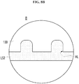
- FIGS. 8A and 8B are enlarged views of part B of the light emitting device illustrated in FIG. 6B .
- FIGS. 6A and 7A are planar views obtained when viewed from a substrate.
- a light emitting device may include a substrate 100, light emitting structures LED each including a first light emitting part LE1, a second light emitting part LE2, and a third light emitting part LE3, which are vertically stacked on a first surface SF1 of the substrate 100, a first light shielding layer LS1 disposed between the light emitting structures LED on the first surface SF1 of the substrate 100, and a second light shielding layer LS2 disposed on a second surface SF2 of the substrate 100 opposing the first surface SF1.
- the first surface SF1 of the substrate 100 may include light emitting areas LEA, in which the light emitting structures LED are disposed, and a light shielding area LSA surrounding the light emitting areas LEA and in which the first light shielding layer LS1 is disposed.
- each light emitting area LEA may have a first width W1.
- the first surface SF1 of the substrate 100 may be substantially flat.
- the first surface SF1 of the substrate 100 may include a plurality of first holes HL1.
- the first holes HL1 disposed in the light shielding area LSA may be filled with the first light shielding layer LS1.
- the inventive concepts are not limited thereto, and in some exemplary embodiments, the first holes HL1 disposed in the light emitting areas LEA may be filled with air.
- first holes HL1 in FIG. 7C are illustrated as being formed on the entire first surface SF1 of the substrate 100, in some exemplary embodiments, the first holes HL1 may be selectively formed only in the light emitting areas LEA of the first surface SF1 of the substrate 100, or may be selectively formed only in the light shielding area LSA of the first surface SF1 of the substrate 100.
- the first holes HL1 may be regularly arranged by being separated from one another by the same distance, and may have the same structure. In some exemplary embodiments, the first holes HL1 may be irregularly arranged, and/or may have different structures.
- each of the first holes HL1 filled with the first light shielding layer LS1 in FIG. 7C is illustrated as having a conical structure, however, in some exemplary embodiments, each of the first holes HL1 may have a cylindrical structure.
- the second surface SF2 of the substrate 100 may include a plurality of second holes HL2.
- each of the second holes HL2 may have substantially a conical structure, as shown in FIG. 8A .
- each of the second holes HL2 may have substantially a cylindrical structure, as shown in FIG. 8B .
- the second holes HL2 may be regularly arranged by being separated from one another by the same distance, and may have the same structure. In some exemplary embodiments, however, the second holes HL2 may be irregularly arranged, and/or may have different structures.
- the second holes HL2 of FIGS. 6B , 7B , and 7C are illustrated as being formed on the entire second surface SF2 of the substrate 100, however, the inventive concepts are not limited thereto.
- the second holes HL2 may be selectively formed only in regions corresponding to light extraction surfaces LEX, may be selectively formed only in regions corresponding to the light emitting areas LEA of the first surface SF1 of the substrate 100, or may be selectively formed only in a region corresponding to the light shielding area LSA of the first surface SF1 of the substrate 100.
- the second light shielding layer LS2 may be disposed in the second holes HL2, and may include openings that at least partially overlap with the light emitting areas LEA.
- the openings may be disposed within the light emitting areas LEA of the first surface SF1 of the substrate 100, and may have a third width W3 less than the first width W1 of the light emitting areas LEA.
- the second surface SF2 of the substrate 100 exposed by the openings may be the light extraction surfaces LEX.
- the light extraction surfaces LEX may have the third width W3 that less than the first width W1 of the light emitting areas LEA.
- the second holes HL2 disposed within the openings of the second light shielding layer LS2 may be exposed to an outside. More particularly, air may be filled in the second holes HL2 disposed within the openings of the second light shielding layer LS2. According to another exemplary embodiment illustrated in FIGS. 7B and 7C , the second light shielding layer LS2 may be filled at least in some of the second holes HL2 disposed within the openings.
- the contrast of light emitting device may be improved. Also, as light is diffusively reflected by the plurality of second holes HL2, which are disposed within the light extraction surfaces LEX, the light extraction of the light emitting device may be improved.
- first holes HL1 which are filled with the first light shielding layer LS1, and the second light shielding layer LS2, which is disposed in a region excluding the light extraction surfaces LEX, may reflect, absorb, and/or shield light generated from neighboring light emitting structures LED, a color mixing may be prevented while improving color reproducibility.
- FIGS. 6A , 6B , 7A , 7B , 7C , 8A , and 8B are substantially the same as those described above with reference to FIGS. 1A , 1B , 1C , 1D , 1E , 2A , 2B , 3A , and 3B , repeated descriptions thereof will be omitted to avoid redundancy.
- FIGS. 9 to 13 are cross-sectional views illustrating a method for manufacturing a light emitting device according to an exemplary embodiment.
- a first n-type semiconductor layer 102, a first active layer 104, a first p-type semiconductor layer 106, and a first ohmic layer 108 may be sequentially formed on a first substrate 100, to form a first light emitting part LE1.
- the first n-type semiconductor layer 102, the first active layer 104, and the first p-type semiconductor layer 106 may be sequentially formed on the first substrate 100 by using a growing method, such as MOCVD (metal organic chemical vapor deposition), MBE (molecular beam epitaxy), HVPE (hydride vapor phase epitaxy), and MOC (metal-organic chloride).
- MOCVD metal organic chemical vapor deposition
- MBE molecular beam epitaxy
- HVPE hydrogen vapor phase epitaxy
- MOC metal-organic chloride
- a second light emitting part LE2 may be formed.
- the second n-type semiconductor layer 202, the second active layer 204, and the second p-type semiconductor layer 206 may be sequentially formed on the second substrate by using a growing method, such as MOCVD, MBE, HVPE, and MOC.
- the second ohmic layer 208 may be formed on the second p-type semiconductor layer 206 through a CVD process, a PVD process, and the like.
- the second ohmic layer 208 may be disposed to face the first ohmic layer 108, and the second light emitting part LE2 may be bonded to the first light emitting part LE1 through a first adhesion part AD1.
- the second substrate may be removed through a laser lift-off (LLO) process or a chemical lift-off (CLO) process.
- LLO laser lift-off
- CLO chemical lift-off
- a third light emitting part LE3 may be formed.
- the third n-type semiconductor layer 302, the third active layer 304, and the third p-type semiconductor layer 306 may be sequentially formed on the third substrate by using a growing method, such as MOCVD, MBE, HVPE, and MOC.
- the third ohmic layer 308 may be formed on the third p-type semiconductor layer 306 through a CVD process, a PVD process, and the like.
- the third substrate may be turned over such that the second n-type semiconductor layer 202 of the second light emitting part LE2 and the third ohmic layer 308 of the third light emitting part LE3 face each other, and the second light emitting part LE2 and the third light emitting part LE3 may be bonded to each other through a second adhesion part AD2. After bonding the second light emitting part LE2 and the third light emitting part LE3 by the second adhesion part AD2, the third substrate may be removed through an LLO or CLO process.
- a first via hole exposing the first ohmic layer 108, a second via hole exposing the second ohmic layer 208, a third via hole exposing the third ohmic layer 308, a fourth via hole exposing the first n-type semiconductor layer 102, a fifth via hole exposing the second n-type semiconductor layer 202, and a sixth via hole exposing the third n-type semiconductor layer 302 may be formed.
- the first light emitting part LE1, the second light emitting part LE2, and the third light emitting part LE3 may be etched to expose the substrate 100, and thus, the light emitting devices may be individually separated from one another.
- a passivation layer PVT may be formed to at least partially fill the first via hole, the second via hole, the third via hole, the fourth via hole, the fifth via hole, and the sixth via hole, and to extend to the top surface of the third n-type semiconductor layer 302.
- the first n-type semiconductor layer 102 may be exposed at the bottom surface of the fourth via hole
- the second n-type semiconductor layer 202 may be exposed at the bottom surface of the fifth via hole
- the third n-type semiconductor layer 302 may be exposed at the bottom surface of the sixth via hole
- the first ohmic layer 108 may be exposed at the bottom surface of the first via hole
- the second ohmic layer 208 may be exposed at the bottom surface of the second via hole
- the third ohmic layer 308 may be exposed at the bottom surface of the third via hole.
- a first via pattern VA1, a second via pattern VA2, a third via pattern VA3, a fourth via pattern VA4, a fifth via pattern VA5, and a sixth via pattern VA6 may be formed in the first via hole, the second via hole, the third via hole, the fourth via hole, the fifth via hole, and the sixth via hole, respectively, along with the passivation layer PVT.
- the first via pattern VA1 may be disposed in the first via hole and be brought into electrical contact with the first ohmic layer 108
- the second via pattern VA2 may be disposed in the second via hole and be brought into electrical contact with the second ohmic layer 208
- the third via pattern VA3 may be disposed in the third via hole and be brought into electrical contact with the third ohmic layer 308
- the fourth via pattern VA4 may be disposed in the fourth via hole and be brought into electrical contact with the first n-type semiconductor layer 102
- the fifth via pattern VA5 may be disposed in the fifth via hole and be brought into electrical contact with the second n-type semiconductor layer 202
- the sixth via pattern VA6 may be disposed in the sixth via hole and be brought into electrical contact with the third n-type semiconductor layer 302.
- the top surface of each of the first via pattern VA1, the second via pattern VA2, the third via pattern VA3, the fourth via pattern VA4, the fifth via pattern VA5, and the sixth via pattern VA6 may be coplanar with the top surface of the passivation layer PVT.
- a first pad PD1 that is brought into electrical contact with the first via pattern VA1 may be formed on the first via pattern VA1
- a second pad PD2 that is brought into electrical contact with the second via pattern VA2 may be formed on the second via pattern VA2
- a third pad PD3 that is brought into electrical contact with the third via pattern VA3 may be formed on the third via pattern VA3
- the fifth via pattern VA5, and the sixth via pattern VA6 may be formed on the fourth via pattern VA4, the fifth via pattern VA5, and the sixth via pattern VA6.
- the light emitting structures LED formed on the substrate 100 may be individualized from one another.
- a first surface SF1 of the substrate 100 may include convex parts CNV covered by the light emitting structure LED, and a concave part CNC from being etched.
- the first surface SF1 of the substrate 100 may not be etched during the etching process, as shown in FIGS. 1C , 1E , and 2B .
- the light emitting structures LED may have inclined sidewalls with a predetermined slope.
- the inventive concepts are not limited thereto, and in some exemplary embodiments, the light emitting structures LED may have the sidewalls that are vertically formed.
- a first light shielding layer LS1 may be disposed between the light emitting structures LED.
- the first light shielding layer LS1 may be formed in the concave part CNC of the first surface SF1 of the substrate 100.
- the first light shielding layer LS1 may cover the sidewalls of the substrate 100 that are formed during the etching process. In this manner, light emitting areas LEA may be defined.
- each of the light emitting structures LED has a width that gradually increases from the third light emitting part LE3 to the first light emitting part LE1
- each of the light emitting areas LEA may have a first width W1 that is substantially the same as the greatest width of each light emitting structure LED.
- the first light shielding layer LS1 may have a top surface disposed on substantially the same level as the top surfaces of the first pad PD1, the second pad PD2, the third pad PD3, and the common pad CPD of the light emitting structure LED.
- the first pad PD1, the second pad PD2, the third pad PD3, and the common pad CPD may not be formed during the process illustrated in FIG. 9 . More particularly, the first pad PD1, the second pad PD2, the third pad PD3 and the common pad CPD may be formed to extend onto the first light shielding layer LS1, after forming the first light shielding layer LS1.
- rough surfaces RGH each including convex and concave pattern CC may be formed.
- the convex and concave pattern CC may be formed.
- the mask pattern may be removed.
- the rough surfaces RGH each including the convex and concave pattern CC may be formed to overlap at least portions of the light emitting areas LEA.
- the rough surfaces RGH may be formed within the light emitting areas LEA, and may have a second width W2 less than the first width W1.
- the center of each rough surface RGH may be concentric with the center of each light emitting area LEA.
- each rough surface RGH may have a second width W2 greater than or equal to the first width W1, as shown in FIG. 1E .
- the center of each rough surface RGH may be concentric with the center of each light emitting area LEA.
- a second light shielding layer LS2 may be formed on the second surface SF2 of the substrate 100.
- the second light shielding layer LS2 having a thin thickness may be formed continuously along the rough surfaces RGH and a flat surface PLT of the second surface SF2 of the substrate 100.
- the first light shielding layer LS1 formed on the concave part CNC of the first surface SF1 of the substrate 100 and the second light shielding layer LS2 formed on the rough surfaces RGH of the second surface SF2 of the substrate 100 may overlap with each other.
- openings that expose portions of the second surface SF2 of the substrate 100 may be formed and define light extraction surfaces LEX, which may have a third width W3 less than the second width W2.
- portions of the rough surfaces RGH from which the second light shielding layer LS2 is removed may be further etched in addition to the etching process illustrated with reference to FIG. 12 .
- portions of the rough surfaces RGH may be secondarily etched to have a roughness different from the portions of the rough surfaces RGH covered by the second light shielding layer LS2, as shown in FIGS. 5A and 5B .
- the portions of the rough surfaces RGH covered by the second light shielding layer LS2 may have a first roughness
- the portions of the rough surfaces RGH exposed by the second light shielding layer LS2 may have a second roughness greater than the first roughness.
- the portions of the rough surfaces RGH covered by the second light shielding layer LS2 may have a first roughness, and the portions of the rough surfaces RGH exposed by the second light shielding layer LS2 may have a second roughness less than the first roughness.
- the rough surfaces RGH may be formed after forming the second light shielding layer LS2.
- the light emitting device may have the structure illustrated in FIGS. 2A and 2B .
Landscapes
- Led Devices (AREA)
- Led Device Packages (AREA)
Abstract
Description
- Exemplary embodiments of the invention relate generally to a light emitting device, and more specifically, to a light emitting device including a plurality of light emitting parts.
- Light emitting diodes, as inorganic light sources, are being diversely used in various fields, such as display devices, vehicle lamps, and general lighting. Light emitting diodes are rapidly replacing existing light sources due to their longer lifetime, lower power consumption, and faster response speed than existing light sources.
- Recently, as light emitting diodes are being developed toward light weight, thin thickness, compactness, and miniaturization to be used as backlight sources of various display devices, such as a mobile phone, a color mixing may occur between neighboring light emitting cells.
- Devices constructed according to exemplary embodiments of the invention are capable of improving light efficiency and light extraction.
- Additional features of the inventive concepts will be set forth in the description which follows, and in part will be apparent from the description, or may be learned by practice of the inventive concepts.
- A light emitting device according to an exemplary embodiment includes a substrate having a first surface and a second surface opposing the first surface, a light emitting structure disposed on the first surface of the substrate and defining a light emitting area, and a first light shielding layer disposed on the second surface of the substrate and exposing at least a portion of the light emitting area, in which the second surface of the substrate has a rough surface that overlaps at least a portion the light emitting area.
- A thickness of a portion of the substrate including the rough surface may be less than a thickness of a portion of the substrate not formed with the rough surface.
- The second surface of the substrate may include a sidewall connected to the rough surface, and the first light shielding layer may extend to the sidewall of the substrate, at least partially cover the rough surface, and define a light extraction surface of the light emitting structure.
- The light extraction surface may have a width less than that of the rough surface and that of the light emitting area.
- The rough surface may include a convex and concave pattern, and a roughness of a portion of the convex and concave pattern formed in the light extraction surface may be different from that of a portion of the convex and concave pattern covered by the first light shielding layer.
- The first light shielding layer may have substantially the same width along the sidewall of the substrate.
- The sidewall of the substrate may be inclined with a predetermined slope, and the first light shielding layer may have a width that gradually decreases from the second surface of the substrate toward an inside of the substrate, and have a side surface vertically extending from the second surface of the substrate.
- The rough surface may be disposed within the light emitting area, and have a width less than the light emitting area.
- The rough surface may cover the light emitting area, and have a width equal to or greater than the light emitting area.
- The light emitting device may further include a second light shielding layer disposed on the first surface of the substrate and surrounding an outer side of the light emitting structure.
- The first surface of the substrate may have a convex part in the light emitting area and a concave part in an area excluding the light emitting area.
- The light emitting device may further include a second light shielding layer disposed in the concave part of the substrate and surrounding an outer side of the light emitting structure.
- A portion of the second light shielding layer disposed in the concave part and a portion of the first light shielding layer covering at least a portion of the rough surface of the substrate may overlap with each other.
- The rough surface may include a plurality of first holes, and at least a portion of the first holes may be disposed in the light emitting area.
- The first light shielding layer may be disposed in the first holes, extend along the second surface of the substrate to cover at least a portion of the light emitting area, and define a light extraction surface of the light emitting structure.
- The light extraction surface may have a width less than that of the light emitting area.
- The first holes formed in the light extraction surface may be filled with air.
- The first holes formed in the light extraction surface may be filled with the first light shielding layer.
- The light emitting device may further include a second light shielding layer disposed on the first surface of the substrate and surrounding an outer side of the light emitting structure.
- The first surface of the substrate may include a plurality of second holes, and the second light shielding layer may be disposed in at least a portion of the second holes.
- The details of other embodiments are included in the detailed description and the drawings.
- In the light emitting device according to the embodiments of the disclosure, since the light generated from a neighboring light emitting structure is prevented from being mixed, by first and second light shielding layers, it is possible to improve color reproducibility.
- Moreover, since a substrate is formed to have a thin thickness only in a region where a rough surface is formed and retain a normal thickness in a remaining region, the substrate may support a plurality of light emitting structures and may not be damaged even by an external shock.
- The light generated by a light emitting structure is diffusively reflected by the rough surface, whereby light efficiency may be improved. Further, as the light shielding layer covers the ends of the rough surface, a light extraction surface may be defined, whereby the contrast of the light emitting device may be improved.
-
-
FIGS. 1A and1B are top views of a light emitting device according to an exemplary embodiment. -
FIGS. 1C ,1D , and1E are cross-sectional views taken along line A-A' ofFIG. 1A according to exemplary embodiments. -
FIG. 2A is a top view of a light emitting device according to another exemplary embodiment. -
FIG. 2B is a cross-sectional view taken along line A-A' ofFIG. 2A . -
FIG. 3A is a top view of a light emitting structure according to an exemplary embodiment. -
FIG. 3B is a cross-sectional view taken along lines A-A' and B-B' ofFIG. 3A . -
FIGS. 4A ,4B ,5A , and5B are cross-sectional views of the structures of rough surfaces and second light shielding layers according to exemplary embodiments. -
FIG. 6A is a top view of a light emitting device according to another exemplary embodiment. -
FIG. 6B is a cross-sectional view taken along line A-A' ofFIG. 6A . -
FIG. 7A is a top view of a light emitting device according to yet another exemplary embodiment. -
FIGS. 7B and7C are cross-sectional views taken along line A-A' ofFIG. 7A according to exemplary embodiments. -
FIGS. 8A and8B are enlarged views for the part B of the light emitting device ofFIG. 6A . -
FIGS. 9 ,10 ,11 ,12 , and13 are cross-sectional views illustrating a method for manufacturing a light emitting device according to an exemplary embodiment. - In order to understand the configuration and effect of the disclosure sufficiently, embodiments of the disclosure will be described with reference to the accompanying drawings. However, the disclosure is not limited to the embodiments set forth herein and may be implemented in various forms, and a variety of changes may be added.
- As used in the embodiments of the disclosure, a technical term may be interpreted as a meaning conventionally known to those of ordinary skill in the art unless defined otherwise.
- Hereinafter, a light emitting device will be described below with reference to the accompanying drawings through various examples of embodiments.
-
FIGS. 1A and1B are top views of a light emitting device according to an exemplary embodiment, andFIGS. 1C ,1D , and IE are cross-sectional views taken along line A-A' ofFIG. 1A according to exemplary embodiments.FIG. 2A is a top view of a light emitting device according to another exemplary embodiment, andFIG. 2B is a cross-sectional view taken along line A-A' ofFIG. 2A .FIG. 3A is a cross-sectional view of a light emitting structure according to an exemplary embodiment, andFIG. 3B is a cross-sectional view taken along lines A-A' and B-B' ofFIG. 3A .FIGS. 4A ,4B ,5A , and5B are cross-sectional views of the structures of rough surfaces and second light shielding layers according to exemplary embodiments. - Referring to
FIGS. 1A ,1B ,1C ,1D ,1E ,2A ,2B ,3A , and3B , a light emitting device may include asubstrate 100 and light emitting structures LED, each including a first light emitting part LE1, a second light emitting part LE2, and a third light emitting part LE3 stacked on thesubstrate 100. -
FIG. 1A is a plan view of the light emitting device when viewed from the third light emitting part LE3, andFIG. 1B is a plan view of the light emitting device when viewed from thesubstrate 100.FIG. 2A is a plan view of the light emitting device when viewed from thesubstrate 100.FIGS. 3A and3B are enlarged views of a light emitting structure. - The
substrate 100 may be capable of growing a gallium nitride-based semiconductor layer thereon, and may include a sapphire (Al2O3), a silicon carbide (SiC), a gallium nitride (GaN), an indium gallium nitride (InGaN), an aluminum gallium nitride (AlGaN), an aluminum nitride (AlN), a gallium oxide (Ga2O3), or silicon. Also, thesubstrate 100 may be a patterned sapphire substrate. According to an exemplary embodiment, thesubstrate 100 may include a material that transmits visible light. - The
substrate 100 may have a first surface SF1 and a second surface SF2 opposing the first surface SF1. A plurality of light emitting structures LED may be disposed on the first surface SF1 of thesubstrate 100 and be spaced apart from each other. Hereinafter, an area in which each light emitting structure LED is disposed is referred to as a light emitting area LEA, and the remaining area in which the light emitting structures LED are not disposed is referred to as a light shielding area LSA. - Referring to
FIGS. 1A ,1C ,1E , and2A , the first surface SF1 of thesubstrate 100 according to exemplary embodiments may be substantially flat. Referring to FIG. ID, the first surface SF1 of thesubstrate 100 according to another exemplary embodiment may have a convex part CNV in each light emitting area LEA, and may have a concave part CNC in the light shielding area LSA. A top surface of each convex part CNV of the first surface SF1 may be disposed at a higher level than a top surface of the concave part CNC. As such, the first surface SF1 may be formed with a stepped part between the convex part CNV and the concave part CNC. - Referring to
FIGS. 1A ,1B ,1C ,1D ,1E ,2A , and2B , the second surface SF2 of thesubstrate 100 may include rough surfaces RGH, each having a convex and concave pattern CC, and a flat surface PLT. Each rough surface RGH may overlap with at least a portion of each light emitting area LEA disposed on the first surface SF1 of thesubstrate 100. - Referring to
FIGS. 1B ,1C ,1D ,2A , and2B , each light emitting area LEA may have a first width W1, and each rough surface RGH may have a second width W2 less than the first width W1. The center of each light emitting area LEA may be concentric with the center of each rough surface RGH. Referring to FIG. IE each light emitting area LEA according to another exemplary embodiment may have a first width W1, and each rough surface RGH may have a second width W2 equal to or greater than the first width W1. The center of each light emitting area LEA may be concentric with the center of each rough surface RGH. - In this manner, since the second surface SF2 of the
substrate 100 has the rough surfaces RGH, light generated from light emitting areas LEA may be diffusively reflected through the rough surfaces RGH, which may improve the light extraction efficiency of the light emitting device. - As shown in
FIGS. 1C ,1D ,1E , and2B , when the first surface SF1 of thesubstrate 100 is substantially flat and the second surface SF2 has the rough surfaces RGH and the flat surface PLT, thesubstrate 100 may have a first thickness TH1 in a portion of the flat surface PLT of the second surface SF2 of thesubstrate 100, and a second thickness TH2 less than the first thickness TH1 in a portion of the second surface SF2 of thesubstrate 100 where the rough surfaces RGH are formed. Due to a thickness difference in thesubstrate 100, sidewalls SDW of thesubstrate 100 may be defined by the ends of the rough surfaces RGH. According to another exemplary embodiment shown inFIG. 1D , when the first surface SF1 of thesubstrate 100 has convex parts CNV and the concave part CNC, and the second surface SF2 has the rough surfaces RGH and the flat surface PLT, the rough surfaces RGH may correspond to the convex parts CNV and overlap with at least portions of the convex parts CNV. Thesubstrate 100 may have a first thickness TH1 between the concave part CNC of the first surface SF1 and the flat surface PLT of the second surface SF2 of thesubstrate 100, and may have a second thickness TH2 less than the first thickness TH1 between the convex part CNV of the first surface SF1 and the rough surface RGH of the second surface SF2 of thesubstrate 100. - In this manner, since the thickness of the
substrate 100 is formed relatively thin in a region where the rough surface RGH is formed, a distance through which light travels through thesubstrate 100 may be decreased. As such, the light emitting structure LED according to exemplary embodiments may reduce an amount of light lost in thesubstrate 100. Further, since the thickness of thesubstrate 100 is relatively thick in a region where the flat surface PLT is formed, thesubstrate 100 may support the light emitting structure LED and may prevent thesubstrate 100 from being damaged from an external shock. - According to an exemplary embodiment, the convex and concave pattern CC of the rough surface RGH may have the same shape and may be arranged regularly. However, the inventive concepts are not limited thereto, and in some exemplary embodiments, the convex and concave pattern CC of the rough surface RGH may have different shapes and/or may be arranged irregularly.
- For example, each sidewall SDW of the
substrate 100, which is defined by the rough surface RGH formed on the second surface SF2 of thesubstrate 100, may have a slope. As such, the space defined between the sidewalls SDW of thesubstrate 100 may have a width that gradually narrows from the second surface SF2 toward the inside of the space. As another example, each sidewall SDW of thesubstrate 100 may be vertical. - Referring to
FIGS. 1A ,1B ,1C ,1D ,1E ,2A ,2B ,3A , and3B , when the second surface SF2 of thesubstrate 100 is a light extraction surface, the wavelength of light emitted from the first light emitting part LE1 may be the shortest, the wavelength of light emitted from the second light emitting part LE2 may be longer than the wavelength of light emitted from the first light emitting part LE1 and be shorter than the wavelength of light emitted from the third light emitting part LE3, and the wavelength of light emitted from the third light emitting part LE3 may be the longest. For example, the first light emitting part LE1 may emit blue light, the second light emitting part LE2 may emit green light, and the third light emitting part LE3 may emit red light. However, the inventive concepts are not limited thereto. For example, in some exemplary embodiments, the second light emitting part LE2 may emit light having a shorter wavelength than light emitted from the first light emitting part LE1. - Referring to
FIGS. 3A and3B , the first light emitting part LE1 may include a first n-type semiconductor layer 102, a firstactive layer 104, a first p-type semiconductor layer 106, and a firstohmic layer 108, the second light emitting part LE2 may include a second n-type semiconductor layer 202, a secondactive layer 204, a second p-type semiconductor layer 206, and a secondohmic layer 208, and the third light emitting part LE3 may include a third n-type semiconductor layer 302, a thirdactive layer 304, a third p-type semiconductor layer 306, and a thirdohmic layer 308. - Each of the first n-
type semiconductor layer 102, the second n-type semiconductor layer 202, and the third n-type semiconductor layer 302 may be a Si-doped gallium nitride-based semiconductor layer. Each of the first p-type semiconductor layer 106, the second p-type semiconductor layer 206, and the third p-type semiconductor layer 306 may be a Mg-doped gallium nitride-based semiconductor layer. Each of the firstactive layer 104, the secondactive layer 204, and the thirdactive layer 304 may include a multi-quantum well (MQW), and the composition ratio thereof may be determined to emit light of a desired peak wavelength. As each of the firstohmic layer 108, the secondohmic layer 208, and the thirdohmic layer 308, a transparent conductive oxide (TCO), such as a tin oxide (SnO), an indium oxide (InO2), a zinc oxide (ZnO), an indium tin oxide (ITO), or indium tin zinc oxide (ITZO) may be used. - The first light emitting part LE1 may be spaced apart from the second light emitting part LE2. For example, the first
ohmic layer 108 of the first light emitting part LE1 may face the secondohmic layer 208 of the second light emitting part LE2. As another example, the firstohmic layer 108 of the first light emitting part LE1 may face the second n-type semiconductor layer 202 of the second light emitting part LE2. - The second light emitting part LE2 may be spaced apart from the third light emitting part LE3. For example, the second
ohmic layer 208 of the second light emitting part LE2 may face the thirdohmic layer 308 of the third light emitting part LE3. As another example, the secondohmic layer 208 of the second light emitting part LE2 may face the third n-type semiconductor layer 302 of the third light emitting part LE3. - The light emitting device may further include a first adhesion part AD1 disposed between the first light emitting part LE1 and the second light emitting part LE2 to bond the first light emitting part LE1 and the second light emitting part LE2, and a second adhesion part AD2 disposed between the second light emitting part LE2 and the third light emitting part LE3 to bond the second light emitting part LE2 and the third light emitting part LE3. Each of the first adhesion part AD1 and the second adhesion part AD2 may include a material that transmits visible light and has an insulating property. Each of the first adhesion part AD1 and the second adhesion part AD2 may include a polymer, a resist, or a polyimide. For example, each of the first adhesion part AD1 and the second adhesion part AD2 may include at least one of SOG (spin-on-glass), BCB (benzo cyclo butadiene), HSQ (hydrogen silsesquioxanes), an SU-8 photoresist, epoxy, PAE (poly arylene ether), such as Flare™, MSSQ (methylsilsesquioxane), PMMA (polymethylmethacrylate), PDMS (polydimethylsiloxane), fluoropolymer, polyimide, MSSQ (methylsilisequioxane), PEEK (polyethereherketone), ATSP (Aromatic Thermosetting Polyester), PVDC (Polyvinylidene chloride), LCP (liquid-crystal polymer), or wax.
- The light emitting device may further include a first color filter CF1 disposed between the first light emitting part LE1 and the second light emitting part LE2, and a second color filter CF2 isposed between the second light emitting part LE2 and the third light emitting part LE3. The first color filter CF1 may be disposed on the first
ohmic layer 108 of the first light emitting part LE1 or the secondohmic layer 208 of the second light emitting part LE2. The second color filter CF2 may be disposed on the second n-type semiconductor layer 202 of the second light emitting part LE2 or the thirdohmic layer 308 of the third light emitting part LE3. The first color filter CF1 may reflect light emitted from the first light emitting part LE1 and pass light emitted from the second light emitting part LE2 and the third light emitting part LE3, so that light emitted from the first light emitting part LE1 does not exert an influence on each of the second light emitting part LE2 and the third light emitting part LE3. The second color filter CF2 may reflect light emitted from the first light emitting part LE1 and the second light emitting part LE2 and pass light emitted from the third light emitting part LE3, so that light emitted from the first light emitting part LE1 and the second light emitting part LE2 does not exert an influence on the third light emitting part LE3. Each of the first color filter CF1 and the second color filter CF2 may include a DBR (distributed Bragg reflector), in which TiO2 and SiO2 are alternately stacked. The first color filter CF1 may be different from the second color filter CF2 in terms of the alternation number and thickness of TiO2 and SiO2. In some exemplary embodiments, at least one of the first color filter CF1 and the second color filter CF2 may be selectively omitted. - The light emitting device may further include a first pad PD1 electrically coupled with the first
ohmic layer 108, a second pad PD2 electrically coupled with the secondohmic layer 208, a third pad PD3 electrically coupled with the thirdohmic layer 308, and a common pad CPD electrically coupled in common with the first n-type semiconductor layer 102, the second n-type semiconductor layer 202, and the third n-type semiconductor layer 302. Referring toFIG. 3A , when viewed from the top, thesubstrate 100 may have a substantially quadrangular structure, and the first pad PD1, the second pad PD2, the third pad PD3, and the common pad CPD may be disposed at the respective corners of thesubstrate 100. - While the first n-
type semiconductor layer 102, the second n-type semiconductor layer 202, and the third n-type semiconductor layer 302 are illustrated as being coupled to the common pad CPD, however, the inventive concepts are not limited thereto. For example, in some exemplary embodiments, the firstohmic layer 108, the secondohmic layer 208, and the thirdohmic layer 308 may be coupled to the common pad CPD. - Referring to
FIGS. 3A and3B , the light emitting device may further include a first via pattern VA1, which passes through the third light emitting part LE3, the second color filter CF2, the second adhesion part AD2, the second light emitting part LE2, the first adhesion part AD1, and the first color filter CF1 and electrically couples the firstohmic layer 108 and the first pad PD1, a second via pattern VA2, which passes through the third light emitting part LE3, the second color filter CF2, the second adhesion part AD2, the second n-type semiconductor layer 202, the secondactive layer 204, and the second p-type semiconductor layer 206 and electrically couples the secondohmic layer 208 and the second pad PD2, and a third via pattern VA3, which passes through the third n-type semiconductor layer 302, the thirdactive layer 304, and the third p-type semiconductor layer 306 and electrically couples the thirdohmic layer 308 and the third pad PD3. Also, the light emitting device may further include a fourth via pattern VA4, which passes through the third light emitting part LE3, the second color filter CF2, the second adhesion part AD2, the second light emitting part LE2, the first adhesion part AD1, the first color filter CF1, the firstohmic layer 108, the first p-type semiconductor layer 106, and the firstactive layer 104 and electrically couples the first n-type semiconductor layer 102 and the common pad CPD, a fifth via pattern VA5, which passes through the third light emitting part LE3, the second color filter CF2, and the second adhesion part AD2 and electrically couples the second n-type semiconductor layer 202 and the common pad CPD, and a sixth via pattern VA6, which passes through a portion of the third n-type semiconductor layer 302 and electrically couples the third n-type semiconductor layer 302 and the common pad CPD. In some exemplary embodiments, the sixth via pattern VA6 may be omitted. - While the light emitting structure LED according to the illustrated exemplary embodiment is illustrated as including the first light emitting part LE1, the second light emitting part LE2, and the third light emitting part LE3, which are vertically stacked, and that the light emitting device includes the via patterns VA1, VA2, VA3, VA4, VA5, and VA6 passing through the first light emitting part LE1, the second light emitting part LE2, and the third light emitting part LE3, however, the inventive concepts are not limited thereto. For example, according to another exemplary embodiments, by etching the vertically stacked first light emitting part LE1, the second light emitting part LE2, and the third light emitting part LE3, the light emitting device may have a structure, which exposes the first n-
type semiconductor layer 102, the second n-type semiconductor layer 202, the third n-type semiconductor layer 302, the firstohmic layer 108, the secondohmic layer 208, and the thirdohmic layer 308. According to still another exemplary embodiment, the light emitting device may have a structure, in which the first light emitting part LE1, the second light emitting part LE2, and the third light emitting part LE3 are horizontally disposed on the same plane. In some exemplary embodiments, the light emitting device may have one light emitting part. - Referring to
FIGS. 1A ,1B ,1C ,1D ,1E ,2A ,2B ,3A , and3B , the light emitting device may further include a first light shielding layer LS1, which surrounds the outer sidewall of each light emitting structure LED on the first surface SF1 of thesubstrate 100 and substantially fills between neighboring light emitting structures LED. The first light shielding layer LS1 may include a material that may shield, absorb, or reflect light generated from each light emitting structure LED and have an insulating property, such that light generated from each light emitting structure LED is not mixed with that from a neighboring light emitting structure LED. For example, the first light shielding layer LS1 may include a material, such as a photoresist, epoxy, PDMS (polydimethylsiloxane), and a black matrix. - The light emitting device may further include a second light shielding layer LS2 having openings that expose at least portions of the rough surfaces RGH on the second surface SF2 of the
substrate 100. Each rough surface RGH exposed by the opening in the second light shielding layer LS2 may be a light extraction surface LEX. The second light shielding layer LS2 may include metal, such as Ti, Ni, Al, Ag, and Cr, or may include a material, such as a photoresist, epoxy, PDMS, and a black matrix. - The light extraction surface LEX according to the illustrated exemplary embodiments is shown as having a quadrangular structure, when viewed from the top as in
FIGS. 1B and2A . However, the inventive concepts are not limited thereto, and in some exemplary embodiments, the light extraction surface LEX may have a substantially polygonal shape, such as substantially a triangular or a circular shape. - Referring back to
FIGS. 2A and2B , the second light shielding layer LS2 according to the illustrated exemplary embodiment may be disposed on the second surface SF2 of thesubstrate 100 while exposing the rough surfaces RGH and not being formed on the sidewalls SDW of thesubstrate 100. More particularly, the second light shielding layer LS2 may not cover the rough surfaces RGH. - Referring back to
FIGS. 1B ,1C ,1D , and1E , the second light shielding layer LS2 according to the illustrated exemplary embodiment may extend from the second surface SF2 of thesubstrate 100 to the sidewalls SDW of thesubstrate 100, and cover the ends of the rough surfaces RGH. The openings of the second light shielding layer LS2 may expose portions of the rough surfaces RGH. The centers of the openings may be concentric with the centers of the rough surfaces RGH. Each rough surface RGH exposed by each opening of the second light shielding layer LS2 may be the light extraction surface LEX. Referring toFIG. 4A , the second light shielding layer LS2 according to an exemplary embodiment may have substantially the same thickness on each sidewall SDW of thesubstrate 100, and may have a sloped side surface on each side of thesubstrate 100. Referring toFIG. 4B , the second light shielding layer LS2 according to another exemplary embodiment may have a thickness that gradually decreases from the second surface SF2 of thesubstrate 100 toward the inside of thesubstrate 100 on each sidewall SDW of thesubstrate 100, such that vertical side surface may be formed on each sidewall SDW of thesubstrate 100. - Referring back to
FIG. 1D , the first light shielding layer LS1, which is disposed on the concave part CNC of the first surface SF1 of thesubstrate 100, and the second light shielding layer LS2, which covers the sidewalls SDW of thesubstrate 100 defined by the rough surfaces RGH, may have an area that overlap with each other. The overlapping area between the first light shielding layer LS1 and the second light shielding layer LS2 may prevent light from being mixed between neighboring light emitting structures LED. - Referring to
FIG. 1E , the second width W2 of each rough surface RGH may be equal to or greater than the first width W1 of the light emitting area LEA, and the second light shielding layer LS2 may cover each rough surface RGH relatively thick to expose the light extraction surface LEX at a third width W3 less that the second width W2 of the light emitting area LEA. Light generated from neighboring light emitting structures LED may be vanished by being diffusively reflected by the convex and concave pattern CC of the rough surface RGH, which are covered by the second light shielding layer LS2, and the remaining light that has not been vanished may be absorbed, shielded, and reflected by the second light shielding layer LS2, so as to prevent a color mixing. - In addition, in each rough surface RGH, the convex and concave pattern CC of the rough surface RGH that are covered by the second light shielding layer LS2 may have a first roughness, and the convex and concave pattern CC of the rough surface RGH exposed by each opening of the second light shielding layer LS2 may have a second roughness different from the first roughness. For example, referring to
FIG. 5A , the first roughness may be greater than the second roughness. As another example, referring toFIG. 5B , the first roughness may be less than the second roughness. - In this manner, light generated from the light emitting structure LED may be emitted through an area reduced by the second light shielding layer LS2. As such, the contrast of light emitting device may be increased, whereby color reproducibility may be improved. Further, the second light shielding layer LS2 together with the first light shielding layer LS1 may prevent light generated from neighboring light emitting structures LED from being mixed, which may prevent a color mixing.
-
FIG. 6A is top view of a light emitting device according to still another exemplary embodiment, andFIG. 6B is a cross-sectional view taken along line A-A' ofFIG. 6A .FIG. 7A is a top view of a light emitting device according to yet still another exemplary embodiment, andFIGS. 7B and7C are cross-sectional views taken along line A-A' ofFIG. 7A .FIGS. 8A and8B are enlarged views of part B of the light emitting device illustrated inFIG. 6B .FIGS. 6A and7A are planar views obtained when viewed from a substrate. - Referring to
FIGS. 6A ,6B ,7A ,7B , and7C , a light emitting device may include asubstrate 100, light emitting structures LED each including a first light emitting part LE1, a second light emitting part LE2, and a third light emitting part LE3, which are vertically stacked on a first surface SF1 of thesubstrate 100, a first light shielding layer LS1 disposed between the light emitting structures LED on the first surface SF1 of thesubstrate 100, and a second light shielding layer LS2 disposed on a second surface SF2 of thesubstrate 100 opposing the first surface SF1. - The first surface SF1 of the
substrate 100 may include light emitting areas LEA, in which the light emitting structures LED are disposed, and a light shielding area LSA surrounding the light emitting areas LEA and in which the first light shielding layer LS1 is disposed. For example, each light emitting area LEA may have a first width W1. - According to exemplary embodiments illustrated in
FIGS. 6B and7B , the first surface SF1 of thesubstrate 100 may be substantially flat. - According to another exemplary embodiment illustrated in
FIG. 7C , the first surface SF1 of thesubstrate 100 may include a plurality of first holes HL1. In this case, the first holes HL1 disposed in the light shielding area LSA may be filled with the first light shielding layer LS1. However, the inventive concepts are not limited thereto, and in some exemplary embodiments, the first holes HL1 disposed in the light emitting areas LEA may be filled with air. - While the first holes HL1 in
FIG. 7C are illustrated as being formed on the entire first surface SF1 of thesubstrate 100, in some exemplary embodiments, the first holes HL1 may be selectively formed only in the light emitting areas LEA of the first surface SF1 of thesubstrate 100, or may be selectively formed only in the light shielding area LSA of the first surface SF1 of thesubstrate 100. The first holes HL1 may be regularly arranged by being separated from one another by the same distance, and may have the same structure. In some exemplary embodiments, the first holes HL1 may be irregularly arranged, and/or may have different structures. - In addition, while each of the first holes HL1 filled with the first light shielding layer LS1 in
FIG. 7C is illustrated as having a conical structure, however, in some exemplary embodiments, each of the first holes HL1 may have a cylindrical structure. - Referring to
FIGS. 6A to 7C , the second surface SF2 of thesubstrate 100 may include a plurality of second holes HL2. According to an exemplary embodiment, each of the second holes HL2 may have substantially a conical structure, as shown inFIG. 8A . According to another exemplary embodiment, each of the second holes HL2 may have substantially a cylindrical structure, as shown inFIG. 8B . - For example, the second holes HL2 may be regularly arranged by being separated from one another by the same distance, and may have the same structure. In some exemplary embodiments, however, the second holes HL2 may be irregularly arranged, and/or may have different structures.
- While the second holes HL2 of
FIGS. 6B ,7B , and7C are illustrated as being formed on the entire second surface SF2 of thesubstrate 100, however, the inventive concepts are not limited thereto. For example, in some exemplary embodiments, the second holes HL2 may be selectively formed only in regions corresponding to light extraction surfaces LEX, may be selectively formed only in regions corresponding to the light emitting areas LEA of the first surface SF1 of thesubstrate 100, or may be selectively formed only in a region corresponding to the light shielding area LSA of the first surface SF1 of thesubstrate 100. - According to an exemplary embodiment, the second light shielding layer LS2 may be disposed in the second holes HL2, and may include openings that at least partially overlap with the light emitting areas LEA. The openings may be disposed within the light emitting areas LEA of the first surface SF1 of the
substrate 100, and may have a third width W3 less than the first width W1 of the light emitting areas LEA. The second surface SF2 of thesubstrate 100 exposed by the openings may be the light extraction surfaces LEX. The light extraction surfaces LEX may have the third width W3 that less than the first width W1 of the light emitting areas LEA. - According to the illustrated exemplary embodiment of
FIG. 6B , the second holes HL2 disposed within the openings of the second light shielding layer LS2 may be exposed to an outside. More particularly, air may be filled in the second holes HL2 disposed within the openings of the second light shielding layer LS2. According to another exemplary embodiment illustrated inFIGS. 7B and7C , the second light shielding layer LS2 may be filled at least in some of the second holes HL2 disposed within the openings. - In this manner, as the second light shielding layer LS2 covers portions of the light emitting areas LEA, and thereby defines the light extraction surfaces LEX having a smaller area, the contrast of light emitting device may be improved. Also, as light is diffusively reflected by the plurality of second holes HL2, which are disposed within the light extraction surfaces LEX, the light extraction of the light emitting device may be improved. By the first light shielding layer LS1 and the second light shielding layer LS2, it is possible to prevent light generated from neighboring light emitting structures LED from being mixed with each other. Since the first holes HL1, which are filled with the first light shielding layer LS1, and the second light shielding layer LS2, which is disposed in a region excluding the light extraction surfaces LEX, may reflect, absorb, and/or shield light generated from neighboring light emitting structures LED, a color mixing may be prevented while improving color reproducibility.
- Since the elements of the light emitting device shown in
FIGS. 6A ,6B ,7A ,7B ,7C ,8A , and8B are substantially the same as those described above with reference toFIGS. 1A ,1B ,1C ,1D ,1E ,2A ,2B ,3A , and3B , repeated descriptions thereof will be omitted to avoid redundancy. - Hereinafter, a method for manufacturing a light emitting device according to an exemplary embodiment will be described. In the illustrated exemplary embodiment, the light emitting device will be described with reference to that shown in
FIGS. 1A ,1B , and1D . -
FIGS. 9 to 13 are cross-sectional views illustrating a method for manufacturing a light emitting device according to an exemplary embodiment. - Referring to
FIG. 9 , a first n-type semiconductor layer 102, a firstactive layer 104, a first p-type semiconductor layer 106, and a firstohmic layer 108 may be sequentially formed on afirst substrate 100, to form a first light emitting part LE1. The first n-type semiconductor layer 102, the firstactive layer 104, and the first p-type semiconductor layer 106 may be sequentially formed on thefirst substrate 100 by using a growing method, such as MOCVD (metal organic chemical vapor deposition), MBE (molecular beam epitaxy), HVPE (hydride vapor phase epitaxy), and MOC (metal-organic chloride). The firstohmic layer 108 may be formed on the first p-type semiconductor layer 106 by using a chemical vapor deposition (CVD) process, physical vapor deposition (PVD), and the like. - By sequentially forming a second n-
type semiconductor layer 202, a secondactive layer 204, a second p-type semiconductor layer 206, and a secondohmic layer 208 on a second substrate, a second light emitting part LE2 may be formed. The second n-type semiconductor layer 202, the secondactive layer 204, and the second p-type semiconductor layer 206 may be sequentially formed on the second substrate by using a growing method, such as MOCVD, MBE, HVPE, and MOC. The secondohmic layer 208 may be formed on the second p-type semiconductor layer 206 through a CVD process, a PVD process, and the like. - By turning over the second substrate, the second
ohmic layer 208 may be disposed to face the firstohmic layer 108, and the second light emitting part LE2 may be bonded to the first light emitting part LE1 through a first adhesion part AD1. After bonding the first light emitting part LE1 and the second light emitting part LE2, the second substrate may be removed through a laser lift-off (LLO) process or a chemical lift-off (CLO) process. - By sequentially forming a third n-
type semiconductor layer 302, a thirdactive layer 304, a third p-type semiconductor layer 306, and a thirdohmic layer 308 on a third substrate(not shown), a third light emitting part LE3 may be formed. The third n-type semiconductor layer 302, the thirdactive layer 304, and the third p-type semiconductor layer 306 may be sequentially formed on the third substrate by using a growing method, such as MOCVD, MBE, HVPE, and MOC. The thirdohmic layer 308 may be formed on the third p-type semiconductor layer 306 through a CVD process, a PVD process, and the like. - The third substrate may be turned over such that the second n-
type semiconductor layer 202 of the second light emitting part LE2 and the thirdohmic layer 308 of the third light emitting part LE3 face each other, and the second light emitting part LE2 and the third light emitting part LE3 may be bonded to each other through a second adhesion part AD2. After bonding the second light emitting part LE2 and the third light emitting part LE3 by the second adhesion part AD2, the third substrate may be removed through an LLO or CLO process. - Then, by etching the third light emitting part LE3, the second light emitting part LE2, and the first light emitting part LE1, a first via hole exposing the first
ohmic layer 108, a second via hole exposing the secondohmic layer 208, a third via hole exposing the thirdohmic layer 308, a fourth via hole exposing the first n-type semiconductor layer 102, a fifth via hole exposing the second n-type semiconductor layer 202, and a sixth via hole exposing the third n-type semiconductor layer 302 may be formed. - According to an exemplary embodiment, while forming the first via hole, the second via hole, the third via hole, the fourth via hole, the fifth via hole, and the sixth via hole, the first light emitting part LE1, the second light emitting part LE2, and the third light emitting part LE3 may be etched to expose the
substrate 100, and thus, the light emitting devices may be individually separated from one another. - A passivation layer PVT may be formed to at least partially fill the first via hole, the second via hole, the third via hole, the fourth via hole, the fifth via hole, and the sixth via hole, and to extend to the top surface of the third n-
type semiconductor layer 302. - By etching the passivation layer PVT, the first n-
type semiconductor layer 102 may be exposed at the bottom surface of the fourth via hole, the second n-type semiconductor layer 202 may be exposed at the bottom surface of the fifth via hole, the third n-type semiconductor layer 302 may be exposed at the bottom surface of the sixth via hole, the firstohmic layer 108 may be exposed at the bottom surface of the first via hole, the secondohmic layer 208 may be exposed at the bottom surface of the second via hole, and the thirdohmic layer 308 may be exposed at the bottom surface of the third via hole. - A first via pattern VA1, a second via pattern VA2, a third via pattern VA3, a fourth via pattern VA4, a fifth via pattern VA5, and a sixth via pattern VA6 may be formed in the first via hole, the second via hole, the third via hole, the fourth via hole, the fifth via hole, and the sixth via hole, respectively, along with the passivation layer PVT.
- The first via pattern VA1 may be disposed in the first via hole and be brought into electrical contact with the first
ohmic layer 108, the second via pattern VA2 may be disposed in the second via hole and be brought into electrical contact with the secondohmic layer 208, the third via pattern VA3 may be disposed in the third via hole and be brought into electrical contact with the thirdohmic layer 308, the fourth via pattern VA4 may be disposed in the fourth via hole and be brought into electrical contact with the first n-type semiconductor layer 102, the fifth via pattern VA5 may be disposed in the fifth via hole and be brought into electrical contact with the second n-type semiconductor layer 202, and the sixth via pattern VA6 may be disposed in the sixth via hole and be brought into electrical contact with the third n-type semiconductor layer 302. - According to an exemplary embodiment, the top surface of each of the first via pattern VA1, the second via pattern VA2, the third via pattern VA3, the fourth via pattern VA4, the fifth via pattern VA5, and the sixth via pattern VA6 may be coplanar with the top surface of the passivation layer PVT.
- A first pad PD1 that is brought into electrical contact with the first via pattern VA1 may be formed on the first via pattern VA1, a second pad PD2 that is brought into electrical contact with the second via pattern VA2 may be formed on the second via pattern VA2, a third pad PD3 that is brought into electrical contact with the third via pattern VA3 may be formed on the third via pattern VA3, and a common pad CPD that is brought into electrical contact in common with the fourth via pattern VA4, the fifth via pattern VA5, and the sixth via pattern VA6 may be formed on the fourth via pattern VA4, the fifth via pattern VA5, and the sixth via pattern VA6.
- Referring to
FIG. 10 , by sequentially etching the third light emitting part LE3, the second light emitting part LE2, and the first light emitting part LE1, the light emitting structures LED formed on thesubstrate 100 may be individualized from one another. - According to an exemplary embodiment, during the etching process, portions of the
substrate 100 under the first light emitting part LE1 may be etched. In this manner, a first surface SF1 of thesubstrate 100 may include convex parts CNV covered by the light emitting structure LED, and a concave part CNC from being etched. However, in some exemplary embodiments, the first surface SF1 of thesubstrate 100 may not be etched during the etching process, as shown inFIGS. 1C ,1E , and2B . - According to an exemplary embodiment, the light emitting structures LED may have inclined sidewalls with a predetermined slope. However, the inventive concepts are not limited thereto, and in some exemplary embodiments, the light emitting structures LED may have the sidewalls that are vertically formed.
- Referring to
FIG. 11 , a first light shielding layer LS1 may be disposed between the light emitting structures LED. According to an exemplary embodiment, the first light shielding layer LS1 may be formed in the concave part CNC of the first surface SF1 of thesubstrate 100. The first light shielding layer LS1 may cover the sidewalls of thesubstrate 100 that are formed during the etching process. In this manner, light emitting areas LEA may be defined. When each of the light emitting structures LED has a width that gradually increases from the third light emitting part LE3 to the first light emitting part LE1, each of the light emitting areas LEA may have a first width W1 that is substantially the same as the greatest width of each light emitting structure LED. - For example, the first light shielding layer LS1 may have a top surface disposed on substantially the same level as the top surfaces of the first pad PD1, the second pad PD2, the third pad PD3, and the common pad CPD of the light emitting structure LED.
- As another example, the first pad PD1, the second pad PD2, the third pad PD3, and the common pad CPD may not be formed during the process illustrated in
FIG. 9 . More particularly, the first pad PD1, the second pad PD2, the third pad PD3 and the common pad CPD may be formed to extend onto the first light shielding layer LS1, after forming the first light shielding layer LS1. - Referring to
FIG. 12 , by etching a second surface SF2 of thesubstrate 100, rough surfaces RGH each including convex and concave pattern CC may be formed. - In particular, by forming a mask pattern on the second surface SF2 of the
substrate 100, and etching the second surface SF2 through wet etching and/or dry etching using the mask pattern as an etch mask, the convex and concave pattern CC may be formed. After forming the rough surfaces RGH, the mask pattern may be removed. - The rough surfaces RGH each including the convex and concave pattern CC may be formed to overlap at least portions of the light emitting areas LEA. According to an exemplary embodiment, the rough surfaces RGH may be formed within the light emitting areas LEA, and may have a second width W2 less than the first width W1. The center of each rough surface RGH may be concentric with the center of each light emitting area LEA. According to another exemplary embodiment, each rough surface RGH may have a second width W2 greater than or equal to the first width W1, as shown in
FIG. 1E . The center of each rough surface RGH may be concentric with the center of each light emitting area LEA. - Referring to
FIG. 13 , a second light shielding layer LS2 may be formed on the second surface SF2 of thesubstrate 100. The second light shielding layer LS2 having a thin thickness may be formed continuously along the rough surfaces RGH and a flat surface PLT of the second surface SF2 of thesubstrate 100. - According to an exemplary embodiment, the first light shielding layer LS1 formed on the concave part CNC of the first surface SF1 of the
substrate 100 and the second light shielding layer LS2 formed on the rough surfaces RGH of the second surface SF2 of thesubstrate 100 may overlap with each other. - Referring back to
FIG. 1D , by etching the second light shielding layer LS2, openings that expose portions of the second surface SF2 of thesubstrate 100 may be formed and define light extraction surfaces LEX, which may have a third width W3 less than the second width W2. - According to an exemplary embodiment, while etching the second light shielding layer LS2, portions of the rough surfaces RGH from which the second light shielding layer LS2 is removed may be further etched in addition to the etching process illustrated with reference to
FIG. 12 . In this manner, portions of the rough surfaces RGH may be secondarily etched to have a roughness different from the portions of the rough surfaces RGH covered by the second light shielding layer LS2, as shown inFIGS. 5A and5B . Referring toFIG. 5A , the portions of the rough surfaces RGH covered by the second light shielding layer LS2 may have a first roughness, and the portions of the rough surfaces RGH exposed by the second light shielding layer LS2 may have a second roughness greater than the first roughness. Referring toFIG. 5B , the portions of the rough surfaces RGH covered by the second light shielding layer LS2 may have a first roughness, and the portions of the rough surfaces RGH exposed by the second light shielding layer LS2 may have a second roughness less than the first roughness. - In some exemplary embodiments, the rough surfaces RGH may be formed after forming the second light shielding layer LS2. When the rough surfaces RGH are formed after forming the second light shielding layer LS2, the light emitting device may have the structure illustrated in
FIGS. 2A and2B . - Although certain exemplary embodiments and implementations have been described herein, other embodiments and modifications will be apparent from this description. Accordingly, the inventive concepts are not limited to such embodiments, but rather to the broader scope of the appended claims and various obvious modifications and equivalent arrangements as would be apparent to a person of ordinary skill in the art.
Claims (20)
- A light emitting device comprising:a substrate having a first surface and a second surface opposing the first surface;a light emitting structure disposed on the first surface of the substrate and defining a light emitting area; anda first light shielding layer disposed on the second surface of the substrate and exposing at least a portion of the light emitting area,wherein the second surface of the substrate has a rough surface that overlaps at least a portion the light emitting area.
- The light emitting device according to claim 1, wherein a thickness of a portion of the substrate including the rough surface is less than a thickness of a portion of the substrate not formed with the rough surface.
- The light emitting device according to claim 1, wherein:the second surface of the substrate includes a sidewall connected to the rough surface; andthe first light shielding layer extends to the sidewall of the substrate, at least partially covers the rough surface, and defines a light extraction surface of the light emitting structure.
- The light emitting device according to claim 3, wherein the light extraction surface has a width less than that of the rough surface and that of the light emitting area.
- The light emitting device according to claim 3, wherein:the rough surface includes a convex and concave pattern; anda roughness of a portion of the convex and concave pattern formed in the light extraction surface is different from that of a portion of the convex and concave pattern covered by the first light shielding layer.
- The light emitting device according to claim 3, wherein the first light shielding layer has substantially the same width along the sidewall of the substrate.
- The light emitting device according to claim 3, wherein:the sidewall of the substrate is inclined with a predetermined slope; andthe first light shielding layer has a width that gradually decreases from the second surface of the substrate toward an inside of the substrate, and has a side surface vertically extending from the second surface of the substrate.
- The light emitting device according to claim 1, wherein the rough surface is disposed within the light emitting area, and has a width less than the light emitting area.
- The light emitting device according to claim 1, wherein the rough surface covers the light emitting area, and has a width equal to or greater than the light emitting area.
- The light emitting device according to claim 1, further comprising a second light shielding layer disposed on the first surface of the substrate and surrounding an outer side of the light emitting structure.
- The light emitting device according to claim 1, wherein the first surface of the substrate has a convex part in the light emitting area and a concave part in an area excluding the light emitting area.
- The light emitting device according to claim 11, further comprising a second light shielding layer disposed in the concave part of the substrate and surrounding an outer side of the light emitting structure.
- The light emitting device according to claim 12, wherein a portion of the second light shielding layer disposed in the concave part and a portion of the first light shielding layer covering at least a portion of the rough surface of the substrate overlap with each other.
- The light emitting device according to claim 1, wherein:the rough surface includes a plurality of first holes; andat least a portion of the first holes are disposed in the light emitting area.
- The light emitting device according to claim 14, wherein the first light shielding layer is disposed in the first holes, extends along the second surface of the substrate to cover at least a portion of the light emitting area, and defines a light extraction surface of the light emitting structure.
- The light emitting device according to claim 15, wherein the light extraction surface has a width less than that of the light emitting area.
- The light emitting device according to claim 15, wherein the first holes formed in the light extraction surface are filled with air.
- The light emitting device according to claim 15, wherein the first holes formed in the light extraction surface are filled with the first light shielding layer.
- The light emitting device according to claim 14, further comprising a second light shielding layer disposed on the first surface of the substrate and surrounding an outer side of the light emitting structure.
- The light emitting device according to claim 19, wherein:the first surface of the substrate includes a plurality of second holes; andthe second light shielding layer is disposed in at least a portion of the second holes.
Applications Claiming Priority (3)
| Application Number | Priority Date | Filing Date | Title |
|---|---|---|---|
| US201862756935P | 2018-11-07 | 2018-11-07 | |
| US16/672,676 US11271136B2 (en) | 2018-11-07 | 2019-11-04 | Light emitting device |
| PCT/KR2019/015090 WO2020096384A1 (en) | 2018-11-07 | 2019-11-07 | Light-emitting diode |
Publications (2)
| Publication Number | Publication Date |
|---|---|
| EP3879584A1 true EP3879584A1 (en) | 2021-09-15 |
| EP3879584A4 EP3879584A4 (en) | 2022-08-03 |
Family
ID=70458746
Family Applications (1)
| Application Number | Title | Priority Date | Filing Date |
|---|---|---|---|
| EP19882208.2A Pending EP3879584A4 (en) | 2018-11-07 | 2019-11-07 | Light-emitting diode |
Country Status (7)
| Country | Link |
|---|---|
| US (3) | US11271136B2 (en) |
| EP (1) | EP3879584A4 (en) |
| JP (1) | JP7500556B2 (en) |
| KR (1) | KR102857446B1 (en) |
| CN (2) | CN210743973U (en) |
| BR (1) | BR112021008898A2 (en) |
| WO (1) | WO2020096384A1 (en) |
Families Citing this family (7)
| Publication number | Priority date | Publication date | Assignee | Title |
|---|---|---|---|---|
| US11282984B2 (en) * | 2018-10-05 | 2022-03-22 | Seoul Viosys Co., Ltd. | Light emitting device |
| US11271136B2 (en) * | 2018-11-07 | 2022-03-08 | Seoul Viosys Co., Ltd | Light emitting device |
| US11211528B2 (en) * | 2019-03-13 | 2021-12-28 | Seoul Viosys Co., Ltd. | Light emitting device for display and display apparatus having the same |
| US11862616B2 (en) * | 2020-02-26 | 2024-01-02 | Seoul Viosys Co., Ltd. | Multi wavelength light emitting device and method of fabricating the same |
| US12080687B2 (en) * | 2020-10-16 | 2024-09-03 | Seoul Viosys Co., Ltd. | Unit pixel having light emitting device, method of fabricating the same, and displaying apparatus having the same |
| JP2025532089A (en) * | 2022-10-06 | 2025-09-29 | エイエムエス-オスラム インターナショナル ゲーエムベーハー | Light-emitting devices |
| WO2025105266A1 (en) * | 2023-11-15 | 2025-05-22 | 日亜化学工業株式会社 | Light-emitting element |
Family Cites Families (32)
| Publication number | Priority date | Publication date | Assignee | Title |
|---|---|---|---|---|
| JP4432275B2 (en) * | 2000-07-13 | 2010-03-17 | パナソニック電工株式会社 | Light source device |
| JP2002289357A (en) | 2001-03-28 | 2002-10-04 | Pioneer Electronic Corp | Organic electroluminescence display panel |
| KR101087567B1 (en) | 2004-03-23 | 2011-11-28 | 엘지디스플레이 주식회사 | Organic electroluminescent device and manufacturing method thereof |
| US8318519B2 (en) * | 2005-01-11 | 2012-11-27 | SemiLEDs Optoelectronics Co., Ltd. | Method for handling a semiconductor wafer assembly |
| US7413918B2 (en) * | 2005-01-11 | 2008-08-19 | Semileds Corporation | Method of making a light emitting diode |
| US7524686B2 (en) * | 2005-01-11 | 2009-04-28 | Semileds Corporation | Method of making light emitting diodes (LEDs) with improved light extraction by roughening |
| JP2008251561A (en) | 2007-03-29 | 2008-10-16 | Toyoda Gosei Co Ltd | Display device |
| WO2009084670A1 (en) * | 2007-12-28 | 2009-07-09 | Nichia Corporation | Semiconductor light emitting element and method for manufacturing the same |
| TWI532214B (en) * | 2010-10-12 | 2016-05-01 | Lg伊諾特股份有限公司 | Light-emitting element and its package |
| KR101769048B1 (en) | 2010-12-22 | 2017-08-17 | 엘지이노텍 주식회사 | Light emitting device, light emitting device package and lighting installation having the same |
| JP5862354B2 (en) * | 2011-04-15 | 2016-02-16 | 三菱化学株式会社 | Nitride-based light-emitting diode device and manufacturing method thereof |
| EP4243094B1 (en) | 2011-09-16 | 2024-05-22 | Seoul Viosys Co., Ltd. | Light emitting diode and patterned substrate for the same |
| KR20140066397A (en) * | 2012-11-23 | 2014-06-02 | 서울바이오시스 주식회사 | Light emitting diode having a plurality of light emitting units |
| JP2014167948A (en) * | 2013-01-30 | 2014-09-11 | Mitsubishi Chemicals Corp | Light-emitting diode element, process of manufacturing the same, and light-emitting apparatus |
| KR102087947B1 (en) * | 2014-07-18 | 2020-03-11 | 엘지이노텍 주식회사 | A light emitting device and a method of manufacturing the same |
| EP3041988B1 (en) * | 2013-09-06 | 2017-07-19 | Teijin Aramid B.V. | Separator paper for electrochemical cells |
| JP2015056650A (en) | 2013-09-13 | 2015-03-23 | 株式会社東芝 | Light-emitting device |
| KR20150102179A (en) | 2014-02-27 | 2015-09-07 | 삼성디스플레이 주식회사 | Display apparatus and a method for manufacturing the same |
| DE102014106585A1 (en) * | 2014-05-09 | 2015-11-12 | Leonhard Kurz Stiftung & Co. Kg | Multilayer body and method for its production |
| US9608168B2 (en) * | 2014-06-13 | 2017-03-28 | Seoul Viosys Co., Ltd. | Light emitting diode |
| JP2016046461A (en) * | 2014-08-26 | 2016-04-04 | 豊田合成株式会社 | Semiconductor light-emitting element wafer, semiconductor light-emitting element and manufacturing method of semiconductor light-emitting element |
| CN108604626B (en) * | 2015-10-19 | 2022-02-18 | 亮锐控股有限公司 | Wavelength-converted light emitting device with textured substrate |
| TWI588984B (en) * | 2016-03-14 | 2017-06-21 | 群創光電股份有限公司 | Display device |
| JP6564348B2 (en) * | 2016-06-06 | 2019-08-21 | 日機装株式会社 | Deep ultraviolet light emitting device |
| JP6428730B2 (en) * | 2016-08-24 | 2018-11-28 | 日亜化学工業株式会社 | Light emitting device |
| JP6871706B2 (en) * | 2016-09-30 | 2021-05-12 | 日機装株式会社 | Manufacturing method of semiconductor light emitting device |
| KR102734057B1 (en) * | 2017-02-24 | 2024-11-26 | 서울바이오시스 주식회사 | Light emitting diode having light blocking layer |
| US10340425B2 (en) * | 2016-11-25 | 2019-07-02 | Seoul Viosys Co., Ltd. | Light emitting diode having light blocking layer |
| JP7255965B2 (en) * | 2017-08-24 | 2023-04-11 | 日機装株式会社 | Method for manufacturing semiconductor light emitting device |
| US11121299B2 (en) * | 2018-10-31 | 2021-09-14 | Taiwan Semiconductor Manufacturing Company, Ltd. | Semiconductor device and method |
| US11271136B2 (en) * | 2018-11-07 | 2022-03-08 | Seoul Viosys Co., Ltd | Light emitting device |
| US11482650B2 (en) * | 2018-11-07 | 2022-10-25 | Seoul Viosys Co., Ltd. | Light emitting device including light shielding layer |
-
2019
- 2019-11-04 US US16/672,676 patent/US11271136B2/en active Active
- 2019-11-07 JP JP2021523199A patent/JP7500556B2/en active Active
- 2019-11-07 EP EP19882208.2A patent/EP3879584A4/en active Pending
- 2019-11-07 WO PCT/KR2019/015090 patent/WO2020096384A1/en not_active Ceased
- 2019-11-07 CN CN201921916450.XU patent/CN210743973U/en active Active
- 2019-11-07 CN CN201980073256.6A patent/CN113056830B/en active Active
- 2019-11-07 KR KR1020217011686A patent/KR102857446B1/en active Active
- 2019-11-07 BR BR112021008898-9A patent/BR112021008898A2/en active Search and Examination
-
2022
- 2022-01-05 US US17/569,219 patent/US11916168B2/en active Active
-
2024
- 2024-01-16 US US18/413,921 patent/US20240154061A1/en active Pending
Also Published As
| Publication number | Publication date |
|---|---|
| BR112021008898A2 (en) | 2021-08-10 |
| CN210743973U (en) | 2020-06-12 |
| KR20210074301A (en) | 2021-06-21 |
| JP2022506047A (en) | 2022-01-17 |
| JP7500556B2 (en) | 2024-06-17 |
| US20200144448A1 (en) | 2020-05-07 |
| EP3879584A4 (en) | 2022-08-03 |
| US20240154061A1 (en) | 2024-05-09 |
| US11271136B2 (en) | 2022-03-08 |
| US11916168B2 (en) | 2024-02-27 |
| CN113056830B (en) | 2024-08-23 |
| CN113056830A (en) | 2021-06-29 |
| WO2020096384A1 (en) | 2020-05-14 |
| KR102857446B1 (en) | 2025-09-09 |
| US20220262982A1 (en) | 2022-08-18 |
Similar Documents
| Publication | Publication Date | Title |
|---|---|---|
| JP7500556B2 (en) | Light-emitting diode | |
| EP4220743B1 (en) | Light emitting diode | |
| EP3879576A1 (en) | Light emitting element | |
| EP3327800B1 (en) | Light emitting diode having a side reflection layer | |
| JP7550146B2 (en) | Light emitting element | |
| US12009466B2 (en) | Light emitting device | |
| JP7536754B2 (en) | Light-emitting device | |
| TWI764528B (en) | Light-emitting element and manufacturing method thereof | |
| TW202230832A (en) | Light-emitting element and manufacturing method thereof |
Legal Events
| Date | Code | Title | Description |
|---|---|---|---|
| STAA | Information on the status of an ep patent application or granted ep patent |
Free format text: STATUS: THE INTERNATIONAL PUBLICATION HAS BEEN MADE |
|
| PUAI | Public reference made under article 153(3) epc to a published international application that has entered the european phase |
Free format text: ORIGINAL CODE: 0009012 |
|
| STAA | Information on the status of an ep patent application or granted ep patent |
Free format text: STATUS: REQUEST FOR EXAMINATION WAS MADE |
|
| 17P | Request for examination filed |
Effective date: 20210604 |
|
| AK | Designated contracting states |
Kind code of ref document: A1 Designated state(s): AL AT BE BG CH CY CZ DE DK EE ES FI FR GB GR HR HU IE IS IT LI LT LU LV MC MK MT NL NO PL PT RO RS SE SI SK SM TR |
|
| DAV | Request for validation of the european patent (deleted) | ||
| DAX | Request for extension of the european patent (deleted) | ||
| A4 | Supplementary search report drawn up and despatched |
Effective date: 20220706 |
|
| RIC1 | Information provided on ipc code assigned before grant |
Ipc: H01L 33/20 20100101ALI20220630BHEP Ipc: H01L 27/15 20060101ALI20220630BHEP Ipc: H01L 33/58 20100101ALI20220630BHEP Ipc: H01L 33/22 20100101AFI20220630BHEP |