CN108604626B - Wavelength-converted light emitting device with textured substrate - Google Patents
Wavelength-converted light emitting device with textured substrate Download PDFInfo
- Publication number
- CN108604626B CN108604626B CN201680074440.9A CN201680074440A CN108604626B CN 108604626 B CN108604626 B CN 108604626B CN 201680074440 A CN201680074440 A CN 201680074440A CN 108604626 B CN108604626 B CN 108604626B
- Authority
- CN
- China
- Prior art keywords
- transparent substrate
- light emitting
- light
- textured
- wavelength converting
- Prior art date
- Legal status (The legal status is an assumption and is not a legal conclusion. Google has not performed a legal analysis and makes no representation as to the accuracy of the status listed.)
- Active
Links
- 239000000758 substrate Substances 0.000 title claims abstract description 141
- 239000004065 semiconductor Substances 0.000 claims abstract description 29
- 239000000463 material Substances 0.000 claims description 64
- 239000010980 sapphire Substances 0.000 claims description 14
- 229910052594 sapphire Inorganic materials 0.000 claims description 14
- 150000004767 nitrides Chemical class 0.000 claims description 7
- 239000007787 solid Substances 0.000 claims description 4
- 239000000945 filler Substances 0.000 claims 5
- 239000010410 layer Substances 0.000 description 38
- 238000000034 method Methods 0.000 description 12
- 239000012790 adhesive layer Substances 0.000 description 10
- 229910052751 metal Inorganic materials 0.000 description 9
- 239000002184 metal Substances 0.000 description 9
- 239000000853 adhesive Substances 0.000 description 8
- 230000001070 adhesive effect Effects 0.000 description 8
- OAICVXFJPJFONN-UHFFFAOYSA-N Phosphorus Chemical compound [P] OAICVXFJPJFONN-UHFFFAOYSA-N 0.000 description 6
- 239000000919 ceramic Substances 0.000 description 6
- 238000006243 chemical reaction Methods 0.000 description 5
- 229920001296 polysiloxane Polymers 0.000 description 5
- 238000005530 etching Methods 0.000 description 4
- 239000002019 doping agent Substances 0.000 description 3
- 230000000694 effects Effects 0.000 description 3
- 239000011521 glass Substances 0.000 description 3
- 238000000227 grinding Methods 0.000 description 3
- 230000000873 masking effect Effects 0.000 description 3
- 239000000203 mixture Substances 0.000 description 3
- 238000001228 spectrum Methods 0.000 description 3
- IJGRMHOSHXDMSA-UHFFFAOYSA-N Atomic nitrogen Chemical compound N#N IJGRMHOSHXDMSA-UHFFFAOYSA-N 0.000 description 2
- 239000004593 Epoxy Substances 0.000 description 2
- GWEVSGVZZGPLCZ-UHFFFAOYSA-N Titan oxide Chemical compound O=[Ti]=O GWEVSGVZZGPLCZ-UHFFFAOYSA-N 0.000 description 2
- 230000002708 enhancing effect Effects 0.000 description 2
- 238000000605 extraction Methods 0.000 description 2
- 239000011888 foil Substances 0.000 description 2
- 230000003287 optical effect Effects 0.000 description 2
- 239000002096 quantum dot Substances 0.000 description 2
- 229910052710 silicon Inorganic materials 0.000 description 2
- 239000010703 silicon Substances 0.000 description 2
- HBMJWWWQQXIZIP-UHFFFAOYSA-N silicon carbide Chemical compound [Si+]#[C-] HBMJWWWQQXIZIP-UHFFFAOYSA-N 0.000 description 2
- 229910010271 silicon carbide Inorganic materials 0.000 description 2
- -1 thickness Substances 0.000 description 2
- 239000012780 transparent material Substances 0.000 description 2
- GYHNNYVSQQEPJS-UHFFFAOYSA-N Gallium Chemical compound [Ga] GYHNNYVSQQEPJS-UHFFFAOYSA-N 0.000 description 1
- 229910010413 TiO 2 Inorganic materials 0.000 description 1
- 238000010521 absorption reaction Methods 0.000 description 1
- 229910052782 aluminium Inorganic materials 0.000 description 1
- XAGFODPZIPBFFR-UHFFFAOYSA-N aluminium Chemical compound [Al] XAGFODPZIPBFFR-UHFFFAOYSA-N 0.000 description 1
- 238000000149 argon plasma sintering Methods 0.000 description 1
- 230000004888 barrier function Effects 0.000 description 1
- 239000011324 bead Substances 0.000 description 1
- 229910002056 binary alloy Inorganic materials 0.000 description 1
- 239000011230 binding agent Substances 0.000 description 1
- 230000005540 biological transmission Effects 0.000 description 1
- 230000015572 biosynthetic process Effects 0.000 description 1
- 238000005422 blasting Methods 0.000 description 1
- 238000005229 chemical vapour deposition Methods 0.000 description 1
- 239000011248 coating agent Substances 0.000 description 1
- 238000000576 coating method Methods 0.000 description 1
- 239000003086 colorant Substances 0.000 description 1
- 239000002131 composite material Substances 0.000 description 1
- 238000005520 cutting process Methods 0.000 description 1
- 239000003989 dielectric material Substances 0.000 description 1
- 239000000975 dye Substances 0.000 description 1
- 229910052733 gallium Inorganic materials 0.000 description 1
- 239000007789 gas Substances 0.000 description 1
- PCHJSUWPFVWCPO-UHFFFAOYSA-N gold Chemical compound [Au] PCHJSUWPFVWCPO-UHFFFAOYSA-N 0.000 description 1
- 239000010931 gold Substances 0.000 description 1
- 229910052737 gold Inorganic materials 0.000 description 1
- 229910052738 indium Inorganic materials 0.000 description 1
- APFVFJFRJDLVQX-UHFFFAOYSA-N indium atom Chemical compound [In] APFVFJFRJDLVQX-UHFFFAOYSA-N 0.000 description 1
- 238000004519 manufacturing process Methods 0.000 description 1
- 238000010297 mechanical methods and process Methods 0.000 description 1
- 230000005226 mechanical processes and functions Effects 0.000 description 1
- 238000012986 modification Methods 0.000 description 1
- 230000004048 modification Effects 0.000 description 1
- 238000001451 molecular beam epitaxy Methods 0.000 description 1
- 239000002159 nanocrystal Substances 0.000 description 1
- 229910052757 nitrogen Inorganic materials 0.000 description 1
- 230000006911 nucleation Effects 0.000 description 1
- 238000010899 nucleation Methods 0.000 description 1
- 239000003973 paint Substances 0.000 description 1
- 238000000059 patterning Methods 0.000 description 1
- 229920000642 polymer Polymers 0.000 description 1
- 239000000843 powder Substances 0.000 description 1
- 239000002243 precursor Substances 0.000 description 1
- 238000002360 preparation method Methods 0.000 description 1
- 230000001681 protective effect Effects 0.000 description 1
- 239000013079 quasicrystal Substances 0.000 description 1
- 229910002059 quaternary alloy Inorganic materials 0.000 description 1
- 238000007493 shaping process Methods 0.000 description 1
- 239000002210 silicon-based material Substances 0.000 description 1
- 229910052709 silver Inorganic materials 0.000 description 1
- 239000004332 silver Substances 0.000 description 1
- 238000005245 sintering Methods 0.000 description 1
- 229910000679 solder Inorganic materials 0.000 description 1
- 238000010345 tape casting Methods 0.000 description 1
- 229910002058 ternary alloy Inorganic materials 0.000 description 1
- 238000001429 visible spectrum Methods 0.000 description 1
- 239000011787 zinc oxide Substances 0.000 description 1
Images

Classifications
-
- H—ELECTRICITY
- H01—ELECTRIC ELEMENTS
- H01L—SEMICONDUCTOR DEVICES NOT COVERED BY CLASS H10
- H01L33/00—Semiconductor devices with at least one potential-jump barrier or surface barrier specially adapted for light emission; Processes or apparatus specially adapted for the manufacture or treatment thereof or of parts thereof; Details thereof
- H01L33/48—Semiconductor devices with at least one potential-jump barrier or surface barrier specially adapted for light emission; Processes or apparatus specially adapted for the manufacture or treatment thereof or of parts thereof; Details thereof characterised by the semiconductor body packages
- H01L33/50—Wavelength conversion elements
- H01L33/505—Wavelength conversion elements characterised by the shape, e.g. plate or foil
-
- H—ELECTRICITY
- H01—ELECTRIC ELEMENTS
- H01L—SEMICONDUCTOR DEVICES NOT COVERED BY CLASS H10
- H01L33/00—Semiconductor devices with at least one potential-jump barrier or surface barrier specially adapted for light emission; Processes or apparatus specially adapted for the manufacture or treatment thereof or of parts thereof; Details thereof
- H01L33/02—Semiconductor devices with at least one potential-jump barrier or surface barrier specially adapted for light emission; Processes or apparatus specially adapted for the manufacture or treatment thereof or of parts thereof; Details thereof characterised by the semiconductor bodies
- H01L33/20—Semiconductor devices with at least one potential-jump barrier or surface barrier specially adapted for light emission; Processes or apparatus specially adapted for the manufacture or treatment thereof or of parts thereof; Details thereof characterised by the semiconductor bodies with a particular shape, e.g. curved or truncated substrate
- H01L33/22—Roughened surfaces, e.g. at the interface between epitaxial layers
-
- H—ELECTRICITY
- H01—ELECTRIC ELEMENTS
- H01L—SEMICONDUCTOR DEVICES NOT COVERED BY CLASS H10
- H01L33/00—Semiconductor devices with at least one potential-jump barrier or surface barrier specially adapted for light emission; Processes or apparatus specially adapted for the manufacture or treatment thereof or of parts thereof; Details thereof
- H01L33/005—Processes
- H01L33/0062—Processes for devices with an active region comprising only III-V compounds
- H01L33/0075—Processes for devices with an active region comprising only III-V compounds comprising nitride compounds
-
- H—ELECTRICITY
- H01—ELECTRIC ELEMENTS
- H01L—SEMICONDUCTOR DEVICES NOT COVERED BY CLASS H10
- H01L33/00—Semiconductor devices with at least one potential-jump barrier or surface barrier specially adapted for light emission; Processes or apparatus specially adapted for the manufacture or treatment thereof or of parts thereof; Details thereof
- H01L33/48—Semiconductor devices with at least one potential-jump barrier or surface barrier specially adapted for light emission; Processes or apparatus specially adapted for the manufacture or treatment thereof or of parts thereof; Details thereof characterised by the semiconductor body packages
- H01L33/483—Containers
- H01L33/486—Containers adapted for surface mounting
-
- H—ELECTRICITY
- H01—ELECTRIC ELEMENTS
- H01L—SEMICONDUCTOR DEVICES NOT COVERED BY CLASS H10
- H01L33/00—Semiconductor devices with at least one potential-jump barrier or surface barrier specially adapted for light emission; Processes or apparatus specially adapted for the manufacture or treatment thereof or of parts thereof; Details thereof
- H01L33/48—Semiconductor devices with at least one potential-jump barrier or surface barrier specially adapted for light emission; Processes or apparatus specially adapted for the manufacture or treatment thereof or of parts thereof; Details thereof characterised by the semiconductor body packages
- H01L33/50—Wavelength conversion elements
- H01L33/501—Wavelength conversion elements characterised by the materials, e.g. binder
- H01L33/502—Wavelength conversion materials
-
- H—ELECTRICITY
- H01—ELECTRIC ELEMENTS
- H01L—SEMICONDUCTOR DEVICES NOT COVERED BY CLASS H10
- H01L33/00—Semiconductor devices with at least one potential-jump barrier or surface barrier specially adapted for light emission; Processes or apparatus specially adapted for the manufacture or treatment thereof or of parts thereof; Details thereof
- H01L33/48—Semiconductor devices with at least one potential-jump barrier or surface barrier specially adapted for light emission; Processes or apparatus specially adapted for the manufacture or treatment thereof or of parts thereof; Details thereof characterised by the semiconductor body packages
- H01L33/58—Optical field-shaping elements
-
- H—ELECTRICITY
- H01—ELECTRIC ELEMENTS
- H01L—SEMICONDUCTOR DEVICES NOT COVERED BY CLASS H10
- H01L2933/00—Details relating to devices covered by the group H01L33/00 but not provided for in its subgroups
- H01L2933/0008—Processes
- H01L2933/0033—Processes relating to semiconductor body packages
- H01L2933/0041—Processes relating to semiconductor body packages relating to wavelength conversion elements
-
- H—ELECTRICITY
- H01—ELECTRIC ELEMENTS
- H01L—SEMICONDUCTOR DEVICES NOT COVERED BY CLASS H10
- H01L2933/00—Details relating to devices covered by the group H01L33/00 but not provided for in its subgroups
- H01L2933/0083—Periodic patterns for optical field-shaping in or on the semiconductor body or semiconductor body package, e.g. photonic bandgap structures
-
- H—ELECTRICITY
- H01—ELECTRIC ELEMENTS
- H01L—SEMICONDUCTOR DEVICES NOT COVERED BY CLASS H10
- H01L2933/00—Details relating to devices covered by the group H01L33/00 but not provided for in its subgroups
- H01L2933/0091—Scattering means in or on the semiconductor body or semiconductor body package
-
- H—ELECTRICITY
- H01—ELECTRIC ELEMENTS
- H01L—SEMICONDUCTOR DEVICES NOT COVERED BY CLASS H10
- H01L33/00—Semiconductor devices with at least one potential-jump barrier or surface barrier specially adapted for light emission; Processes or apparatus specially adapted for the manufacture or treatment thereof or of parts thereof; Details thereof
- H01L33/48—Semiconductor devices with at least one potential-jump barrier or surface barrier specially adapted for light emission; Processes or apparatus specially adapted for the manufacture or treatment thereof or of parts thereof; Details thereof characterised by the semiconductor body packages
- H01L33/52—Encapsulations
- H01L33/56—Materials, e.g. epoxy or silicone resin
-
- H—ELECTRICITY
- H01—ELECTRIC ELEMENTS
- H01L—SEMICONDUCTOR DEVICES NOT COVERED BY CLASS H10
- H01L33/00—Semiconductor devices with at least one potential-jump barrier or surface barrier specially adapted for light emission; Processes or apparatus specially adapted for the manufacture or treatment thereof or of parts thereof; Details thereof
- H01L33/48—Semiconductor devices with at least one potential-jump barrier or surface barrier specially adapted for light emission; Processes or apparatus specially adapted for the manufacture or treatment thereof or of parts thereof; Details thereof characterised by the semiconductor body packages
- H01L33/58—Optical field-shaping elements
- H01L33/60—Reflective elements
Abstract
Embodiments of the present invention include a flip-chip semiconductor light emitting device and a wavelength converting structure disposed in a path of light extracted from the flip-chip semiconductor light emitting device. The substrate with the textured top surface is positioned with the bottom surface facing the wavelength converting structure. The wavelength converting structure is disposed between the substrate and the flip-chip semiconductor light emitting device.
Description
Cross Reference to Related Applications
This application claims priority from U.S. provisional patent application No. 62/243,470 filed on day 19/10/2015. U.S. provisional patent application No. 62/243,470 is incorporated herein.
Technical Field
The present invention relates to a wavelength converted light emitting device having a substrate with a textured surface, the substrate being positioned in the path of light extracted from a wavelength converting structure.
Background
Semiconductor light emitting devices including Light Emitting Diodes (LEDs), Resonant Cavity Light Emitting Diodes (RCLEDs), vertical cavity laser diodes (VCSELs), and edge emitting lasers are among the most efficient light sources currently available. In the manufacture of high brightness light emitting devices capable of operation across the visible spectrum, materials systems currently of interest include group III-V semiconductors, particularly binary, ternary, and quaternary alloys of gallium, aluminum, indium, and nitrogen, also referred to as ill-nitride materials. Group III nitride light emitting devices are typically fabricated by epitaxially growing a stack of semiconductor layers of different compositions and dopant concentrations on a sapphire, silicon carbide, group III nitride, or other suitable substrate using Metal Organic Chemical Vapor Deposition (MOCVD), Molecular Beam Epitaxy (MBE), or other epitaxial techniques. The stack often includes one or more n-type layers doped with, for example, Si, formed over a substrate, one or more light emitting layers in an active region formed over the n-type layer(s), and one or more p-type layers doped with, for example, Mg, formed over the active region. Electrical contacts are formed on the n-type and p-type regions.
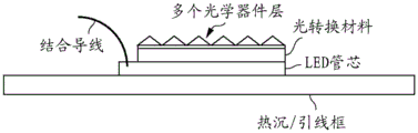
White light may be created by positioning a wavelength converting material in the path of light extracted from the LED. Fig. 1 illustrates one example of a wavelength converting LED described in more detail in US 2013/0258634. US 2013/0258634 teaches the device "of fig. 1 to include a microstructured film formed over the LED and a light conversion material formed over the LED and under the film. The light conversion material may comprise a layer of light phosphor, which may be deposited directly on the LED or may be placed on the LED or attached to the LED as a layer of a pre-formed film. This structure can be used in white LED light devices where the light conversion material converts the LED light to white light. On top of the light conversion material layer and the structure of the LED, a layer of a light deflecting film having a microstructure is formed. Photons emitted from the LED and photons emitted at the phosphor layer due to absorption of the LED light interact with the top deflection film and reflect back and forth within the structure to create a light shaping effect, wherein light reflects between the LED and the light deflection film and exits the top deflection film in a selected direction defined by the microstructures in the deflection film. The deflection film may also induce a light focusing effect on light exiting the deflection film, and the light focusing may depend on the optical refractive index of the deflection film. The geometry of the deflection film may also affect the light focusing. ".
Disclosure of Invention
It is an object of the invention to provide a wavelength converted light emitting device with a textured substrate, which may at least partially collimate light extracted from a wavelength converting structure.
Embodiments of the present invention include a flip-chip semiconductor light emitting device and a wavelength converting structure disposed in a path of light extracted from the flip-chip semiconductor light emitting device. The substrate with the textured top surface is positioned with the bottom surface facing the wavelength converting structure. The wavelength converting structure is disposed between the substrate and the flip-chip semiconductor light emitting device.
Embodiments of the present invention include a semiconductor light emitting device and a wavelength converting structure disposed in a path of light extracted from the semiconductor light emitting device. The substrate is arranged in the path of light extracted from the wavelength converting structure. The substrate includes a body and a dielectric layer disposed on the body. The top surface of the dielectric layer is textured.
Drawings
Fig. 1 illustrates a prior art structure including an LED die, a light conversion material, and an optics layer.
Fig. 2 is a cross-sectional view of an LED.
Fig. 3 is a cross-sectional view of a device including an LED, a wavelength converting structure, and a textured substrate.
Fig. 4 illustrates a bottom surface of the textured substrate of fig. 3.
Fig. 5 is a cross-sectional view of a device including an LED, a wavelength converting structure, and a substrate including a textured dielectric material grown on a body.
Fig. 6 is a cross-sectional view of the device of fig. 5 without a gap between the substrate and the wavelength converting structure.
Fig. 7 is a cross-sectional view of an apparatus including a plurality of textured substrates.
FIG. 8 is a plot of cross-sectional far-field intensity for a device having a textured substrate.
Detailed Description
In embodiments of the present invention, a wavelength converting semiconductor light emitting device, such as a semiconductor light emitting diode, is combined with a substrate having a textured surface.
Fig. 2 illustrates one example of a group III nitride LED. Any suitable semiconductor light emitting apparatus may be used, and embodiments of the present invention are not limited to the LED illustrated in fig. 2. Further, although the semiconductor light emitting device is a group III nitride LED that emits blue or UV light in the following examples, semiconductor light emitting devices other than LEDs (such as laser diodes) and semiconductor light emitting devices made of other material systems (such as other group III-V materials, group III phosphide, group III arsenide, group II-VI materials, ZnO, or Si-based materials) may be used.
In the device of fig. 2, most of the light is extracted from the LED through the growth substrate. Such devices may be referred to as flip chip devices. The LED of fig. 2 is formed by growing a group III nitride semiconductor structure on a growth substrate 10 as is known in the art. The growth substrate is often sapphire, but may be any suitable substrate, such as, for example, a non-III-nitride material, SiC, Si, GaN, or a composite substrate. The surface of the growth substrate on which the group III nitride semiconductor structure is grown may be patterned, roughened, or textured prior to growth, which may improve light extraction from the device. The surface of the growth substrate opposite the growth surface (i.e., the surface through which most of the light is extracted in a flip chip configuration) may be patterned, roughened, or textured before or after growth, which may improve light extraction from the device.
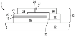
The semiconductor structure includes a light emitting or active region sandwiched between n-type and p-type regions. n-type region 16 may be grown first and may include multiple layers of different compositions and dopant concentrations, including, for example, preparation layers such as buffer layers or nucleation layers (which may be n-type or unintentionally doped) and n-type or even p-type device layers designed for specific optical, material, or electrical characteristics that are desirable for the light emitting region to emit light efficiently. A light emitting or active region 18 is grown over the n-type region. Examples of suitable light emitting regions include a single thick or thin light emitting layer or multiple quantum well light emitting regions comprising multiple thin or thick light emitting layers separated by barrier layers. P-type region 20 may then be grown over the light emitting region. Like the n-type region, the p-type region may include multiple layers of different composition, thickness, and dopant concentration, including layers that are not intentionally doped or n-type layers.
After growth of the semiconductor structure, a reflective p-contact is formed on the surface of the p-type region. The p-contact 21 often includes multiple conductive layers, such as a reflective metal and a protective metal that may prevent or reduce electromigration of the reflective metal. The reflective metal is often silver, but any suitable material or materials may be used. After forming p-contact 21, portions of p-contact 21, p-type region 20, and active region 18 are removed to expose portions of n-type region 16, on which n-contact 22 is formed. The n-contact 22 and the p-contact 21 are electrically isolated from each other by a gap 25 that may be filled with a dielectric, such as an oxide of silicon or any other suitable material. A plurality of n-contact vias may be formed; the n-contact 22 and the p-contact 21 are not limited to the arrangement illustrated in fig. 2. The n-contacts and p-contacts may be redistributed to form bond pads (bond pads) with a dielectric/metal stack, as is known in the art.
To electrically and physically attach the LED to another structure, one or more interconnects 26 and 28 are formed on or electrically connected to the n-contact 22 and the p-contact 21. In fig. 3 interconnect 26 is electrically connected to n-contact 22. The interconnect 28 is electrically connected to the p-contact 21. Interconnects 26 and 28 are electrically isolated from n-contact 22 and p-contact 21 and from each other by dielectric layer 24 and gap 27. Interconnects 26 and 28 may be, for example, solder, bumps, gold layers, or any other suitable structure. Many individual LEDs are formed on a single wafer and then diced from the wafer of the device. The substrate 10 may be thinned after growth of the semiconductor structure or after formation of the individual devices. In some embodiments, the substrate is removed from the apparatus of fig. 2. Most of the light extracted from the device of fig. 2 is extracted through the substrate 10 (or the surface of the semiconductor structure exposed by removing the substrate 10). In the following figures, the LEDs are represented by the block 1. The structures formed on substrate 10, including semiconductor structures, metal and dielectric layers, are represented by block 12. Embodiments of the invention are not limited to flip-chip LEDs-any suitable device may be used.
In the embodiments described below, the wavelength converting structure may be arranged in the path of light extracted from the light emitting device. The wavelength converting structure comprises one or more wavelength converting materials which may be, for example, conventional phosphors, organic phosphors, quantum dots, organic semiconductors, group II-VI or III-V semiconductor quantum dots or nanocrystals, dyes, polymers or other materials that emit light. The wavelength converting material absorbs light emitted by the LED and emits light of one or more different wavelengths. The unconverted light emitted by the LED is often part of the final spectrum of light extracted from the structure, although this is not required. The final spectrum of light extracted from the structure may be white, polychromatic or monochromatic. Examples of common combinations include blue emitting LEDs combined with yellow emitting wavelength converting materials, blue emitting LEDs combined with green and red emitting wavelength converting materials, UV emitting LEDs combined with blue and yellow emitting wavelength converting materials, and UV emitting LEDs combined with blue, green and red emitting wavelength converting materials. Wavelength converting materials that emit light of other colors may be added to adjust the spectrum of light extracted from the structure. The wavelength converting structure may include a light scattering or light diffusing element, such as TiO 2.
In some embodiments, the wavelength converting structure is a structure that is fabricated separately from the LED and attached to the LED, for example by wafer bonding or a suitable adhesive (such as silicone or epoxy). One example of such a prefabricated wavelength converting element is a ceramic phosphor, which is formed, for example, by sintering a powder phosphor or a precursor material of the phosphor into a ceramic plate, which may then be cut into individual wavelength converting elements. The ceramic phosphor may also be formed, for example, by tape casting, where the ceramic is manufactured into the correct shape without cutting or chipping. Examples of suitable non-ceramic pre-formed wavelength converting elements include powdered phosphors (which are wound, cast or otherwise formed into sheets and then divided into individual wavelength converting elements) dispersed in a transparent material such as silicone or glass, and phosphors mixed with silicone and disposed on a transparent substrate.
In the following figures, the wavelength converting structure is represented by block 2.
In some embodiments, wavelength-converted LEDs are combined with structures for enhancing directional emission (i.e., brightness at the normal to the major surface of the LED), which can enhance the brightness of the device. The structure for enhancing directional emission may be, for example, a textured substrate, as illustrated in fig. 3, 5, 6, and 7.
As used herein, "textured" may refer to a surface that is roughened (randomly textured) or patterned (textured in an ordered and/or repeating manner). The cross-section of the textured surface may include peaks or high points (hill) separated by valleys. As illustrated in the following figures, the "peaks" may be triangular in cross-section, although this is not required. In some embodiments, the texturing-forming features may be cones, pyramids, truncated cones, truncated pyramids, pillars, or any other suitable structure, including Johnson solid (Johnson solid) or near Johnson solid. The bottoms of the features may touch adjacent features, or the features may be spaced apart from each other. The features may be arranged in any array, such as, for example, a triangular, square, hexagonal, quasi-crystal, or any other suitable array. The characteristic peak-to-peak spacing may be at least 500 nm in some embodiments, at least 5000 nm in some embodiments, and no greater than 50 μm in some embodiments.
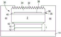
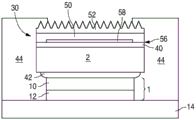
Fig. 3 is a cross-sectional view of one embodiment including a textured substrate 30. In the device of fig. 3, the LED 1 is attached to the submount 14 such that the substrate 10 is arranged furthest away from the submount 14. The base may be, for example, silicon, ceramic, metal, printed circuit board, or any other suitable material. The wavelength converting structure 2 is arranged in the path of the light emitted by the LED 1. In some embodiments, the wavelength converting structure 2 is formed directly on the LED 1. In some embodiments, the wavelength converting structure 2 is formed separately from the LED 1 and attached to the substrate 10 of the LED 1 by any suitable technique, including wafer bonding and bonding with an adhesive layer 42. The adhesive layer 42 may be any suitable material that adheres the wavelength converting structure to the LED 1, is transparent, and does not significantly degrade when exposed to the operating conditions of the LED 1 and when exposed to light extracted from the LED 1 and the wavelength converting structure 2. Silicone, epoxy, glass, and non-III-nitride materials are examples of suitable binders 42.
The textured substrate 30 is arranged in the path of light extracted from the wavelength converting structure 2 such that the wavelength converting structure 2 is arranged between the LED 1 and the substrate 30. The top surface of substrate 30 (i.e., the surface of substrate 30 from which most of the light is extracted from the substrate) is textured surface 32. Substrate 30 may be at least 100 μm thick in some embodiments, no greater than 300 μm thick in some embodiments, and 200 μm thick in some embodiments. The textured portion may have a depth of at least 1 μm in some embodiments, and not greater than 10 μm in some embodiments. The bottom surface of the substrate 30 is located near the wavelength converting structure 2. In some embodiments, the substrate 30 is attached to the wavelength converting structure 2 by any suitable technique, including wafer bonding and adhesion with an adhesive layer 40. Suitable adhesives may be the same as described above for adhesive layer 42. The adhesive layers 40 and 42 may be the same material or different materials.
In some embodiments, the substrate 30 is formed and/or attached to the wavelength converting structure 2 such that a gap 38 is formed between the wavelength converting structure 2 and the substrate 30. The gap 38 may be filled with air, ambient gas, or any other suitable material. The gap 38 may be at least 10 μm thick in some embodiments, and no greater than 200 μm thick in some embodiments.
The light may be collimated by the gap 38. Light exiting the structure travels from the high index region (e.g., wavelength converting structure 2, which may be YAG: Ce, having a refractive index of at least 1.8) to the low index region (e.g., air in gap 38, having a refractive index of 1) to the second high index region (e.g., substrate 30, which may be sapphire, having a refractive index of at least 1.7). Because only light at certain angles of incidence is able to pass through an interface of materials with different indices of refraction without undergoing total internal reflection, the interface collimates the light. The higher the refractive index difference (particularly between the low refractive index region and the second high refractive index region), the greater the collimating effect, although greater collimation may be at the expense of lower transmission. The difference in refractive index between the high index regions (substrate 10 and textured substrate 30) and the low index regions (material in gap 38) is at least 0.5 in some embodiments, and at least 0.6 in some embodiments.
In some embodiments, the gap 38 is formed by placing adhesive 40 only at one or more edges of the wavelength converting structure 2, leaving the gap 38 where the adhesive 40 is not placed. In such embodiments, the substrate 30 may have a flat bottom surface.
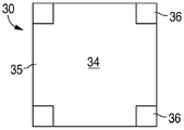
In some embodiments, the bottom surface 35 of the substrate 30 is formed to create a gap 38, as illustrated in fig. 4. On a bottom surface 35 of the substrate 30 illustrated in fig. 4, the substrate 30 is shaped by any suitable technique, such as, for example, masking and etching or a mechanical process such as grinding, to form one or more pillars 36. In the embodiment illustrated in fig. 4, four square posts 36 are disposed at the corners of the substrate 30. More or fewer posts may be used and the posts may be placed in different places, including away from the edge of the substrate 30. The posts need not be square as illustrated, they may be any suitable shape. On the remainder of the bottom surface 35, in the region 34 between the pillars 36, the bottom of the substrate is recessed relative to the pillars. In other words, substrate 30 is thicker where pillars 36 are formed and thinner in regions 34 where there are no pillars. When the substrate is attached to the wavelength converting structure 2 or the adhesive 40, only the posts 36 are in direct contact with the wavelength converting structure 2 or the adhesive 40, leaving gaps 38. The post 36 may be of any suitable size and shape. In one example, the column 36 is no greater than 50 μm x 50 μm wide and between 10 μm and 200 μm high.
The substrate 30 may be any suitable material that is transparent, does not significantly degrade when exposed to the operating conditions of the LED 1 and when exposed to light extracted from the LED 1 and the wavelength converting structure 2, and is suitable for forming a textured surface and posts on the bottom surface. In some embodiments, substrate 30 may have a refractive index of at least 1.5. Examples of suitable materials include sapphire and glass.
The posts 36 and gaps 38 on the textured surface 32 and the bottom of the substrate 30 may be formed by any suitable technique, including, for example, masking and etching, and mechanical techniques such as grinding.
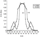
Fig. 8 illustrates cross sections of far field intensity for a device as illustrated in fig. 3 (curve 90) and a device without a textured substrate (curve 92). As illustrated in fig. 8, light extracted from the device illustrated in fig. 3 is more collimated than light extracted from a reference device without a textured substrate. In some applications, the light may be more collimated in only some planes. In the example of an automotive headlamp, for example, the collimation curve illustrated in fig. 8 may represent light emitted along a plane perpendicular to the road. The beam horizontal to the road may still be wide.
In some embodiments, a reflective material is disposed on the sides of one or more of the LED 1, the wavelength converting structure 2, and the substrate 30. In the embodiment illustrated in fig. 3, the reflective material 44 is disposed on the sides of all three structures. In some embodiments, the reflective material may be arranged on only the sides of the LED 1 and/or the wavelength converting structure 2, or the reflective material may be arranged on portions of the sidewalls of any of the three structures. The reflective material 44 may be, for example, TiO2 disposed in a transparent material such as silicone, a reflective coating or foil (such as a metal foil) or reflective paint disposed on the sidewalls, or any other suitable material. The reflective material 44 may be molded over the structure including the LED 1, the wavelength converting structure 2, and the textured substrate 30, pressed over the structure, or formed by any other suitable technique. Excess reflective material disposed over the top of textured surface 32 may be removed by, for example, bead blasting or any other suitable technique.
Fig. 5 and 6 are cross-sectional views of other embodiments including a textured substrate. The LED 1, the submount 14, the wavelength converting structure 2, the adhesive layers 40 and 42, and the reflective material 44 in fig. 5 and 6 may be the same as described above with respect to fig. 3.
In the apparatus of fig. 5 and 6, the substrate 30 includes a body 50 and a dielectric layer 52. The top surface of dielectric layer 52 is textured. The textured surface of the dielectric layer 52 may have the same shape and dimensions as described above with respect to fig. 3. Dielectric layer 52 may be grown or otherwise deposited on a major surface of body 50. The surface of the body 50 on which the dielectric layer 52 is formed may be planar or may itself be textured (not shown).
In some embodiments, body 50 is transparent, is suitable for forming and patterning dielectric layer 52, and is as inexpensive as possible. In some embodiments, the body 50 and the dielectric layer 52 are selected to have relatively high refractive indices, in some embodiments at least 2. In some embodiments, body 50 is a non-III-nitride material (such as sapphire) and dielectric layer 52 is a non-doped III-nitride material (such as GaN). The GaN layer may be grown on the sapphire body and then roughened or patterned using any suitable technique, such as, for example, mechanical techniques (such as grinding), masking and etching, or techniques that form a randomly textured surface (such as photoelectrochemical etching). The GaN layer 52 typically does not include a light emitting layer.
In the embodiment illustrated in fig. 5, at the bottom surface 56 of the body 50, a gap 58 is formed between the body 50 and the adhesive layer 40 (if used) or the wavelength converting structure 2 (if no adhesive layer is used). The gap may be the same as the gap described above with respect to fig. 3, and may be formed in the same manner as the gap described above with respect to fig. 3. In fig. 6, there is no gap. In fig. 6, both the top surface of the wavelength converting structure 2 and the bottom surface of the body 50 are flat surfaces.
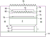
In the embodiment illustrated in fig. 7, a plurality of substrates having textured top surfaces are disposed over the LEDs and the wavelength converting structures. The LED 1, the submount 14, the wavelength converting structure 2, the adhesive layers 40 and 42, and the reflective material 44 in fig. 7 may be the same as described above with respect to fig. 3. The substrate may be a textured substrate, as described above with respect to fig. 3, or may be a substrate comprising a body and a textured dielectric layer, as described above with respect to fig. 5 and 6.
The first substrate 70 is attached to the wavelength converting structure 2, for example by an adhesive layer 40. At least a portion of the top surface 72 of the first substrate 70 is textured. The second substrate 74 is attached to the first substrate 70. The top surface 76 of the second substrate 74 is textured. The second substrate 74 may be attached to the first substrate by adhesive 82 or by any other suitable method or material.
In some embodiments, the second substrate 74 is formed with one or more posts on a bottom surface like the substrate described in FIG. 3, which form a gap 80 between the first and second substrates. The top surface 72 of the first substrate 70 may be textured such that the regions on the second substrate 74 where the posts touch the top surface 72 of the first substrate 70 are not textured, or the posts may be placed on the textured surface 72. The adhesive 82 may be disposed in the region of the posts on the bottom surface of the second substrate 74 in order to attach the first substrate 70 to the second substrate 74. In the embodiment illustrated in fig. 7, gaps 78 and 80 are formed between the wavelength converting structure 2 and the first substrate 70, and between the first substrate 70 and the second substrate 74. Either or both of gaps 78 and 80 may be omitted.
Having described the invention in detail, those skilled in the art will appreciate that, given the present disclosure, modifications may be made to the invention without departing from the spirit of the inventive concept described herein. In particular, features described in particular embodiments may be combined in any embodiment and features may be deleted from embodiments. Therefore, it is not intended that the scope of the invention be limited to the specific embodiments illustrated and described.
Claims (20)
1. A light emitting device comprising:
a semiconductor light emitting structure;
a wavelength converting structure comprising a planar light output surface facing away from the semiconductor light emitting structure, the wavelength converting structure being arranged to absorb light emitted by the semiconductor light emitting structure and in response emit light of a different wavelength through the planar light output surface;
a transparent substrate comprising a planar light input surface arranged parallel to and facing the planar light output surface of the wavelength converting structure, an opposing textured light output surface facing away from the wavelength converting structure, and a post extending towards and facing the planar light output surface of the wavelength converting structure, the post being attached to the wavelength converting structure and defining a gap between the planar light input surface of the transparent substrate and the planar light output surface of the wavelength converting structure; and
a filler material disposed in and filling a gap between the planar light input surface of the transparent substrate and the planar light output surface of the wavelength converting structure, the filler material having a refractive index lower than a refractive index of the wavelength converting structure and lower than a refractive index of the transparent substrate.
2. The light emitting device of claim 1, wherein the filler material disposed in and filling the gap is air.
3. The light emitting device of claim 1, wherein a refractive index of the filler material disposed in and filling the gap is at least 0.5 less than a refractive index of the transparent substrate and at least 0.5 less than a refractive index of the wavelength converting structure.
4. The light emitting apparatus of claim 1, wherein the gap has a width perpendicular to a light output surface of the wavelength converting structure that is greater than or equal to 10 microns and less than or equal to 200 microns.
5. The light emitting device of claim 1, wherein the textured light output surface of the transparent substrate partially collimates light entering the transparent substrate from the wavelength converting structure and exiting the transparent substrate through the textured light output surface of the transparent substrate.
6. The light emitting device of claim 1, wherein the textured light output surface of the transparent substrate comprises features arranged in an array, wherein a peak-to-peak spacing between features is greater than or equal to 500 nanometers.
7. The light emitting device of claim 6, wherein the feature has a shape selected from the group consisting of a pillar, a pyramid, a cone, a truncated pyramid, a truncated cone, and any near Johnson solid.
8. The light emitting device of claim 1, wherein the transparent substrate is sapphire and the textured light output surface of the transparent substrate is a textured sapphire surface.
9. The light emitting apparatus of claim 1 wherein the transparent substrate comprises a sapphire block and a textured layer of high index material disposed on the sapphire block, and the textured light output surface of the transparent substrate is a surface of the textured layer of high index material.
10. The light emitting device of claim 9, wherein the high index material is a group III nitride material.
11. The light emitting device of claim 9, wherein the high index material is GaN.
12. The light emitting device of claim 1, wherein the transparent substrate is a first transparent substrate, the light emitting device further comprising:
a second transparent substrate arranged with a light input surface of the second transparent substrate facing the textured light output surface of the first transparent substrate and an opposing textured light output surface facing away from the first transparent substrate, a first portion of the light input surface of the second transparent substrate attached to the first transparent substrate and a second portion of the light input surface of the second transparent substrate spaced apart from the textured light output surface of the first transparent substrate, the second portion of the light input surface of the second transparent substrate and the textured light output surface of the first transparent substrate defining a gap between the second transparent substrate and the first transparent substrate; and
a second filling material that is provided in a gap between the second transparent substrate and the first transparent substrate and fills the gap between the second transparent substrate and the first transparent substrate, the second filling material having a refractive index lower than a refractive index of the second transparent substrate and lower than a refractive index of the first transparent substrate.
13. The light-emitting device according to claim 12, wherein the second filling material which is provided in a gap between the second transparent substrate and the first transparent substrate and fills the gap between the second transparent substrate and the first transparent substrate is air.
14. The light-emitting device according to claim 12, wherein a refractive index of the second filler material which is provided in the gap between the second transparent substrate and the first transparent substrate and fills the gap between the second transparent substrate and the first transparent substrate is at least 0.5 smaller than a refractive index of the first transparent substrate and at least 0.5 smaller than a refractive index of the second transparent substrate.
15. The light emitting apparatus of claim 1, wherein:
the filling material disposed in and filling the gap is air; and is
The gap has a width perpendicular to a light output surface of the wavelength converting structure that is greater than or equal to 10 microns and less than or equal to 200 microns.
16. The light emitting device of claim 12, wherein the second portion of the light input surface of the second transparent substrate and the light output surface of the wavelength converting structure are parallel.
17. The light emitting device of claim 15, wherein the textured light output surface of the transparent substrate comprises features arranged in an array, wherein a peak-to-peak spacing between features is greater than or equal to 500 nanometers.
18. The light emitting apparatus of claim 17, wherein the transparent substrate is sapphire and the textured light output surface of the transparent substrate is a textured sapphire surface.
19. The light emitting apparatus of claim 17, wherein the transparent substrate comprises a sapphire block and a textured layer of high index material disposed on the sapphire block, and the textured light output surface of the transparent substrate is a surface of the textured layer of high index material.
20. The light emitting apparatus of claim 1 wherein the planar light input surface in contact with the gap is a planar surface.
Applications Claiming Priority (3)
| Application Number | Priority Date | Filing Date | Title |
|---|---|---|---|
| US201562243470P | 2015-10-19 | 2015-10-19 | |
| US62/243470 | 2015-10-19 | ||
| PCT/US2016/056284 WO2017069964A1 (en) | 2015-10-19 | 2016-10-10 | Wavelength converted light emitting device with textured substrate |
Publications (2)
| Publication Number | Publication Date |
|---|---|
| CN108604626A CN108604626A (en) | 2018-09-28 |
| CN108604626B true CN108604626B (en) | 2022-02-18 |
Family
ID=57153584
Family Applications (1)
| Application Number | Title | Priority Date | Filing Date |
|---|---|---|---|
| CN201680074440.9A Active CN108604626B (en) | 2015-10-19 | 2016-10-10 | Wavelength-converted light emitting device with textured substrate |
Country Status (6)
| Country | Link |
|---|---|
| US (1) | US11005012B2 (en) |
| EP (1) | EP3365925B1 (en) |
| JP (1) | JP6852066B2 (en) |
| CN (1) | CN108604626B (en) |
| TW (1) | TWI745309B (en) |
| WO (1) | WO2017069964A1 (en) |
Families Citing this family (9)
| Publication number | Priority date | Publication date | Assignee | Title |
|---|---|---|---|---|
| JP6719424B2 (en) * | 2017-06-26 | 2020-07-08 | 日機装株式会社 | Semiconductor light emitting device and method for manufacturing semiconductor light emitting device |
| EP3785307A1 (en) * | 2018-04-23 | 2021-03-03 | Cree, Inc. | Semiconductor light emitting devices including superstrates with patterned surfaces |
| US11333320B2 (en) * | 2018-10-22 | 2022-05-17 | American Sterilizer Company | Retroreflector LED spectrum enhancement method and apparatus |
| DE102018127521A1 (en) * | 2018-11-05 | 2020-05-07 | Osram Opto Semiconductors Gmbh | Optoelectronic semiconductor component and method for producing an optoelectronic semiconductor component |
| US11271136B2 (en) * | 2018-11-07 | 2022-03-08 | Seoul Viosys Co., Ltd | Light emitting device |
| TWI786503B (en) * | 2020-12-29 | 2022-12-11 | 晶元光電股份有限公司 | Light-emitting device and manufacturing method thereof |
| DE102021119003A1 (en) * | 2021-07-22 | 2023-01-26 | OSRAM Opto Semiconductors Gesellschaft mit beschränkter Haftung | OPTOELECTRONIC SEMICONDUCTOR ELEMENT AND OPTOELECTRONIC COMPONENT |
| US20230317896A1 (en) | 2022-03-31 | 2023-10-05 | Nichia Corporation | Light-emitting device |
| WO2023189384A1 (en) * | 2022-03-31 | 2023-10-05 | ソニーグループ株式会社 | Light-emitting device and image display device |
Citations (3)
| Publication number | Priority date | Publication date | Assignee | Title |
|---|---|---|---|---|
| CN1886841A (en) * | 2003-11-25 | 2006-12-27 | 松下电工株式会社 | Light emitting device using light emitting diode chip |
| CN102347428A (en) * | 2010-07-28 | 2012-02-08 | Lg伊诺特有限公司 | Light emitting device package |
| WO2014203793A1 (en) * | 2013-06-17 | 2014-12-24 | ヘンケル・アクチェンゲゼルシャフト・ウント・コムパニー・コマンディットゲゼルシャフト・アウフ・アクチェン | Light emitting device, sealing film laminate for producing same, and method for manufacturing light emitting device |
Family Cites Families (22)
| Publication number | Priority date | Publication date | Assignee | Title |
|---|---|---|---|---|
| DE10351397A1 (en) | 2003-10-31 | 2005-06-16 | Osram Opto Semiconductors Gmbh | LED chip |
| JP4821087B2 (en) | 2003-11-28 | 2011-11-24 | パナソニック電工株式会社 | Light emitting device |
| TWI303110B (en) * | 2003-11-25 | 2008-11-11 | Matsushita Electric Works Ltd | Light-emitting device using light-emitting diode chip |
| JP2005209795A (en) | 2004-01-21 | 2005-08-04 | Koito Mfg Co Ltd | Light emitting module and lighting tool |
| US7514721B2 (en) * | 2005-11-29 | 2009-04-07 | Koninklijke Philips Electronics N.V. | Luminescent ceramic element for a light emitting device |
| JP2008251561A (en) | 2007-03-29 | 2008-10-16 | Toyoda Gosei Co Ltd | Display |
| US20090173958A1 (en) * | 2008-01-04 | 2009-07-09 | Cree, Inc. | Light emitting devices with high efficiency phospor structures |
| DE102008025756B4 (en) * | 2008-05-29 | 2023-02-23 | OSRAM Opto Semiconductors Gesellschaft mit beschränkter Haftung | semiconductor device |
| JP2011233650A (en) | 2010-04-26 | 2011-11-17 | Toshiba Corp | Semiconductor light-emitting device |
| WO2012006123A2 (en) | 2010-06-28 | 2012-01-12 | Axlen Technologies, Inc. | Optical beam shaping and polarization selection on led with wavelength conversion |
| JP2012109532A (en) * | 2010-09-08 | 2012-06-07 | Mitsubishi Chemicals Corp | Light emitting apparatus, lighting apparatus, and lens |
| US8492788B2 (en) | 2010-10-08 | 2013-07-23 | Guardian Industries Corp. | Insulating glass (IG) or vacuum insulating glass (VIG) unit including light source, and/or methods of making the same |
| US20120112218A1 (en) * | 2010-11-04 | 2012-05-10 | Agency For Science, Technology And Research | Light Emitting Diode with Polarized Light Emission |
| CN102683538B (en) * | 2011-03-06 | 2016-06-08 | 维亚甘有限公司 | LED package and manufacture method |
| JP5862354B2 (en) | 2011-04-15 | 2016-02-16 | 三菱化学株式会社 | Nitride-based light-emitting diode device and manufacturing method thereof |
| TWI475729B (en) | 2011-07-14 | 2015-03-01 | Univ Nat Taiwan Science Tech | Polarized white light emitting diode |
| US8946747B2 (en) * | 2012-02-13 | 2015-02-03 | Cree, Inc. | Lighting device including multiple encapsulant material layers |
| WO2013144798A1 (en) * | 2012-03-30 | 2013-10-03 | Koninklijke Philips N.V. | Optical cavity including a light emitting device and wavelength converting material |
| US20140016299A1 (en) | 2012-06-14 | 2014-01-16 | Solar Science, Co., Ltd. | Photon enhancement guiding structures, devices, and methods for light emitting devices |
| EP2896077B1 (en) * | 2012-09-17 | 2019-01-16 | Lumileds Holding B.V. | Light emitting device including shaped substrate |
| CN106796977B (en) * | 2014-07-23 | 2019-06-28 | 晶体公司 | The photon of ultraviolet light emitting device extracts |
| KR20160124375A (en) * | 2015-04-17 | 2016-10-27 | 삼성전자주식회사 | Method of manufacturing semiconductor light emitting device package |
-
2016
- 2016-10-10 WO PCT/US2016/056284 patent/WO2017069964A1/en active Application Filing
- 2016-10-10 CN CN201680074440.9A patent/CN108604626B/en active Active
- 2016-10-10 US US15/769,134 patent/US11005012B2/en active Active
- 2016-10-10 EP EP16784364.8A patent/EP3365925B1/en active Active
- 2016-10-10 JP JP2018520130A patent/JP6852066B2/en active Active
- 2016-10-19 TW TW105133739A patent/TWI745309B/en active
Patent Citations (3)
| Publication number | Priority date | Publication date | Assignee | Title |
|---|---|---|---|---|
| CN1886841A (en) * | 2003-11-25 | 2006-12-27 | 松下电工株式会社 | Light emitting device using light emitting diode chip |
| CN102347428A (en) * | 2010-07-28 | 2012-02-08 | Lg伊诺特有限公司 | Light emitting device package |
| WO2014203793A1 (en) * | 2013-06-17 | 2014-12-24 | ヘンケル・アクチェンゲゼルシャフト・ウント・コムパニー・コマンディットゲゼルシャフト・アウフ・アクチェン | Light emitting device, sealing film laminate for producing same, and method for manufacturing light emitting device |
Also Published As
| Publication number | Publication date |
|---|---|
| WO2017069964A1 (en) | 2017-04-27 |
| EP3365925B1 (en) | 2021-04-14 |
| JP6852066B2 (en) | 2021-03-31 |
| JP2018531517A (en) | 2018-10-25 |
| TW201727946A (en) | 2017-08-01 |
| US20180315901A1 (en) | 2018-11-01 |
| US11005012B2 (en) | 2021-05-11 |
| TWI745309B (en) | 2021-11-11 |
| CN108604626A (en) | 2018-09-28 |
| KR20180070673A (en) | 2018-06-26 |
| EP3365925A1 (en) | 2018-08-29 |
Similar Documents
| Publication | Publication Date | Title |
|---|---|---|
| CN108604626B (en) | Wavelength-converted light emitting device with textured substrate | |
| US10957821B2 (en) | Wavelength converted semiconductor light emitting device | |
| EP2984685B1 (en) | Fabrication method for top emitting semiconductor light emitting devices | |
| JP2018531517A6 (en) | Wavelength-converting light-emitting device with textured substrate | |
| TWI734110B (en) | Lighting structure and method of manufactureing a light emitting device | |
| CN105393373B (en) | Light emitting device with optical element and reflector | |
| JP6305337B2 (en) | Semiconductor structure processing method | |
| JP7361810B2 (en) | Light emitting device on mount with reflective layer | |
| KR102657885B1 (en) | Wavelength-converted light-emitting device with textured substrate | |
| US20220254962A1 (en) | Optical arrangements in cover structures for light emitting diode packages and related methods | |
| CN104904010B (en) | Luminescent device including filter and protective layer |
Legal Events
| Date | Code | Title | Description |
|---|---|---|---|
| PB01 | Publication | ||
| PB01 | Publication | ||
| SE01 | Entry into force of request for substantive examination | ||
| SE01 | Entry into force of request for substantive examination | ||
| GR01 | Patent grant | ||
| GR01 | Patent grant |