EP3876272A1 - Package for containing electronic component, and electronic device - Google Patents
Package for containing electronic component, and electronic device Download PDFInfo
- Publication number
- EP3876272A1 EP3876272A1 EP19878889.5A EP19878889A EP3876272A1 EP 3876272 A1 EP3876272 A1 EP 3876272A1 EP 19878889 A EP19878889 A EP 19878889A EP 3876272 A1 EP3876272 A1 EP 3876272A1
- Authority
- EP
- European Patent Office
- Prior art keywords
- frame
- substrate
- electronic component
- plan
- view
- Prior art date
- Legal status (The legal status is an assumption and is not a legal conclusion. Google has not performed a legal analysis and makes no representation as to the accuracy of the status listed.)
- Withdrawn
Links
Images


Classifications
-
- H—ELECTRICITY
- H10—SEMICONDUCTOR DEVICES; ELECTRIC SOLID-STATE DEVICES NOT OTHERWISE PROVIDED FOR
- H10W—GENERIC PACKAGES, INTERCONNECTIONS, CONNECTORS OR OTHER CONSTRUCTIONAL DETAILS OF DEVICES COVERED BY CLASS H10
- H10W76/00—Containers; Fillings or auxiliary members therefor; Seals
- H10W76/60—Seals
-
- H—ELECTRICITY
- H10—SEMICONDUCTOR DEVICES; ELECTRIC SOLID-STATE DEVICES NOT OTHERWISE PROVIDED FOR
- H10W—GENERIC PACKAGES, INTERCONNECTIONS, CONNECTORS OR OTHER CONSTRUCTIONAL DETAILS OF DEVICES COVERED BY CLASS H10
- H10W76/00—Containers; Fillings or auxiliary members therefor; Seals
- H10W76/10—Containers or parts thereof
- H10W76/17—Containers or parts thereof characterised by their materials
- H10W76/18—Insulating materials, e.g. resins, glasses or ceramics
-
- H—ELECTRICITY
- H10—SEMICONDUCTOR DEVICES; ELECTRIC SOLID-STATE DEVICES NOT OTHERWISE PROVIDED FOR
- H10W—GENERIC PACKAGES, INTERCONNECTIONS, CONNECTORS OR OTHER CONSTRUCTIONAL DETAILS OF DEVICES COVERED BY CLASS H10
- H10W42/00—Arrangements for protection of devices
- H10W42/121—Arrangements for protection of devices protecting against mechanical damage
-
- H—ELECTRICITY
- H10—SEMICONDUCTOR DEVICES; ELECTRIC SOLID-STATE DEVICES NOT OTHERWISE PROVIDED FOR
- H10W—GENERIC PACKAGES, INTERCONNECTIONS, CONNECTORS OR OTHER CONSTRUCTIONAL DETAILS OF DEVICES COVERED BY CLASS H10
- H10W76/00—Containers; Fillings or auxiliary members therefor; Seals
- H10W76/10—Containers or parts thereof
- H10W76/12—Containers or parts thereof characterised by their shape
-
- H—ELECTRICITY
- H10—SEMICONDUCTOR DEVICES; ELECTRIC SOLID-STATE DEVICES NOT OTHERWISE PROVIDED FOR
- H10W—GENERIC PACKAGES, INTERCONNECTIONS, CONNECTORS OR OTHER CONSTRUCTIONAL DETAILS OF DEVICES COVERED BY CLASS H10
- H10W76/00—Containers; Fillings or auxiliary members therefor; Seals
- H10W76/10—Containers or parts thereof
- H10W76/12—Containers or parts thereof characterised by their shape
- H10W76/15—Containers comprising an insulating or insulated base
Definitions
- the present disclosure relates to an electronic component accommodation package for accommodating an electronic component, and an electronic device.
- thermal deformation may cause a tilt in the vertical direction or input/output terminals and the like to be subjected to a load.
- An electronic component accommodation package includes: a substrate that has an upper surface including an mounting area on which an electronic component is to be mounted; a frame that is on the upper surface of the substrate to surround the mounting area and that has a through hole that penetrates the frame outward from the mounting area in a plan view.
- the frame includes: a first frame that is on the upper surface of the substrate to surround at least a part of the mounting area and that contains a ceramic material; a second frame that is on the upper surface of the substrate to surround at least a part of the mounting area, that has the through hole, and that contains a metal material; and a third frame that is on an upper surface of the first frame and an upper surface of the second frame to surround the mounting area in a plan view and that contains a metal material.
- the first frame incudes a first end and a second end, and the second frame includes a third end and a fourth end. The first end of the first frame and the fourth end of the second frame are joined to each other via a joining material, and the second end of the first frame and the third end of the second frame are joined to each other via a joining material.
- the electronic device includes: the above-described electronic component accommodation package; an electronic component mounted on the mounting area; and a lid that covers the electronic component and that is bonded on an upper surface of the third frame via an adhesive.
- the electronic component accommodation package 1 (hereinafter referred to as the package 1) will be described referring to FIG. 1 to FIG. 4 and FIG. 6 .
- the package 1 is used for accommodating an element composed of a passive element.
- Such elements include, for example, active elements such as semiconductor elements, transistors, diodes and thyristors, resistors, capacitors, solar cells, piezoelectric elements, crystal oscillators, ceramic oscillators, and the like. More specifically, the package 1 is suitable for an element compatible with high voltage, large current, high speed and high frequency to be mounted therein to exhibit the function.
- an electronic component such as a semiconductor element is mounted.
- the electronic device 10 is the package 1 with an electronic component such as a semiconductor element mounted therein as an example of the element.
- the package 1 includes a substrate 2 and a frame 11.
- the frame 11 includes a first frame 3, a second frame 4, and a third frame 7.
- the first frame 3 is on the upper surface 24 of the substrate 2.
- the second frame 4 is joined to the first frame 3.
- the third frame 7 is on the upper surface of the first frame 3 and the upper surface of the second frame 4.
- the second frame 4 has a through hole O in a side wall.
- the through hole O penetrates the side wall outward from an mounting area 21 in a plan view.
- the substrate 2 has, for example, a rectangular shape in a plan view. As illustrated in FIG. 4 , the upper surface 24 of the substrate 2 includes a mounting area 21 on which the electronic component 5 is to be mounted and a peripheral area 22 surrounding the mounting area 21.
- the substrate 2 may be made of, for example, a metal material such as copper, iron, tungsten, molybdenum, nickel or cobalt, or an alloy containing any of these metal materials.
- the substrate 2 may have a function of efficiently dissipating the heat generated in the package 1 by the electronic component 5 to the outside of the package 1.
- the substrate 2 may have good thermal conductivity.
- the thermal conductivity of the substrate 2 can be, for example, 15 W/(m ⁇ K) or more and 450 W/(m ⁇ K) or less.
- the coefficient of thermal expansion of the substrate 2 may be, for example, 3 ⁇ 10 -6 /K or more and 28 ⁇ 10 -6 /K or less.
- the substrate 2 is manufactured into a predetermined shape by applying metal working such as rolling or punching to an ingot that is obtained by casting a molten metal material into a mold and solidifying it.
- the length of each side of the substrate 2 in a plan view is, for example, 5 m or more and 50 mm or less. More specifically, as illustrated in FIG. 4 , the substrate 2 may have a rectangular shape with a first long side 2L1, a second long side 2L2, a first short side 2S1, and a second short side 2S2 in a plan view.
- the first long side 2L1 and the second long side 2L2 may be, for example, 10 mm or more and 50 mm or less
- the first short side 2S1 and the second short side 2S2 may be, for example, 5 mm or more and 20 mm or less
- the thickness of the substrate 2 in the vertical direction (direction orthogonal to the upper surface 24 of the substrate 2) is, for example, 0.3 mm or more and 5 mm or less.
- a metal layer of nickel, gold or the like may be formed on the surface of the substrate 2 by electroplating or electroless plating.
- the thickness of the metal layer is, for example, 0.5 ⁇ m or more and 9 ⁇ m or less.
- the frame 11 is on the upper surface 24 of the substrate 2 to surround the mounting area 21.
- the frame 11 includes the first frame 3, the second frame 4, and the third frame 7.
- the first frame 3 is on the upper surface 24 of the substrate 2 along the peripheral area 22 of the substrate 2.
- the first frame 3 may serve as an input/output terminal and can exchange signals between the internal electronic component 5 and the outside.
- the first frame 3 has, for example, a U shape in a plan view and may surround the inside from three directions. That is, the first frame 3 may be any member that is on the upper surface 24 of the substrate 2 to surround at least a part of the mounting area 21.
- the first frame 3 may include a frame-shaped flat plate portion 31 and a frame-shaped wall portion 32 disposed on the flat plate portion 31.
- the flat plate portion 31 may have a protruding portion 31a protruding outward from the outer edge of the substrate 2 in a plan view.
- a signal wiring 33 may be disposed on the upper surface of the protruding portion 31a. This allows the package 1 to be readily connected to an external electric circuit board via the protruding portion 31a.
- the external electric circuit board may be, for example, a flexible board.
- the frame-shaped flat plate portion 31 of the first frame 3 includes a plate-shaped part in contact with the substrate 2 and a U-shaped frame part on the plate-shaped part. Even in this shape, the first frame 3 is disposed to surround at least a part of the mounting area 21 of the substrate 2.
- the first frame 3 may include a metallized layer (not shown) that is on the under surface of the flat plate portion 31 and joined to the substrate 2, the signal wiring 33 on the upper surface of the flat plate portion 31, a metal layer (not shown) on the upper surface of the wall portion 32, and a ground layer 34 on the upper surfaces of the flat plate portion 31 and the wall portion 32.
- the signal wiring 33 is provided for electric conduction between the inside and outside of the package 1. Further, the signal wiring 33 is a base for connecting a lead terminal or the like provided on the outside of the package 1.
- the metal layer is a base for joining the second frame 4, which will be described later, by a metal joining material such as a brazing material or solder.
- the flat plate portion 31 has a rectangular shape in a plan view.
- the wall portion 32 has a shape that is obtained by removing one side from a frame in a plan view.
- the flat plate portion 31 and the wall portion 32 may be integrally formed in one piece.
- an insulating layer for further wiring a signal line may be provided between the flat plate portion 31 and the wall portion 32.
- the first frame 3 can be freely and suitably configured according to the design of the signal wiring and the like of the package 1.
- the first frame 3 contains a ceramic material.
- the flat plate portion 31 and the wall portion 32 are made of an insulating material, for example a ceramic material such as an alumina-based sintered body, a mullite-based sintered body, a silicon carbide-based sintered body, an aluminum nitride-based sintered body, and a silicon nitride-based sintered body, or glass ceramics.
- the signal wiring 33 and the metal layer may be constituted by a base of a high-melting-point metal material such as tungsten, molybdenum or manganese and a plating layer of nickel, gold or the like formed thereon.
- the coefficient of thermal expansion of the flat plate portion 31 or the wall portion 32 containing a ceramic material is, for example, 3 ⁇ 10 -6 /K or more and 8 ⁇ 10 -6 /K or less.
- a method of manufacturing the first frame 3 will be described.
- a plurality of signal wirings 33 and the ground layer 34 are formed along a side of the upper surface of the flat plate portion 31, for example, by screen printing.
- the metal layer and the ground layer 34 are formed by screen printing.
- the wall portion 32, on which the unsintered metal layer and ground layer 34 before being fired are formed is pressure-bonded onto on the flat plate portion 31, on which the unsintered signal wirings 33 and ground layer 34 before being fired are formed, and the wall portion 32 and the flat plate portion 31 are fired simultaneously.
- the first frame 3 can be manufactured in this way.
- each signal wiring 33 appears to be divided into two parts by the wall portion 32, but the signal wiring 33 is continuous directly under the wall portion 32. Accordingly, in a plan view of the first frame 3, the part of each signal wiring 33 located inside the package 1 is electrically continuous with the part of the signal wiring 33 located outside the package 1. This allows the electronic component 5 in the package 1 to be connected to an electric circuit board outside the package 1 via the signal wirings 33.
- the length of each side of the flat plate portion 31 is, for example, 3 mm or more and 50 mm or less.
- the height of the flat plate portion 31 is, for example, 1 mm or more and 10 mm or less.
- the length of each side of the wall portion 32 is, for example, 1 mm or more and 50 mm or less.
- the height of the wall portion 32 is, for example, 1 mm or more and 10 mm or less.
- Lead terminals may be electrically connected on the signal wirings 33 via a brazing material.
- the lead terminals are provided for electric connection to an external electric circuit board or the like.
- the second frame 4 is joined to the upper surface 24 of the substrate 2 along the peripheral area 22 of the substrate 2 and is provided for protecting the electronic component 5 from the outside as with the first frame 3.
- the second frame 4 may have a frame shape, for example, formed in a U-shape in a plan view.
- the second frame 4 may have a shape that surrounds the inside from three directions. That is, the second frame 4 may be any member that is on the upper surface 24 of the substrate 2 to surround at least a part of the mounting area 21. Further, the second frame 4 may have the through hole O.
- the second frame 4 is brazed to the upper surface 24 of the substrate 2 via a brazing material.
- This shape facilitates the processing of the second frame 4, for example, compared to a second frame 4 that has a shape of surrounding all four sides and has an opening on a wall. As a result, the productivity can be improved. Further, also with regard to joining to the first frame 3, this shape can reduce the joining area, which can reduce mutual influence due to thermal deformation.
- the second frame 4 contains a metal material. More specifically, the second frame 4 is made of, for example, a metal material such as copper, iron, tungsten, molybdenum, nickel or cobalt, or an alloy containing any of these metal materials. The second frame 4 may have a function of efficiently dissipating the heat generated in the package by the electronic component 5 1 to the outside of the package 1.
- the thermal conductivity of the second frame 4 is, for example, 15 W/(m ⁇ K) or more and 450 W/(m ⁇ K) or less.
- the coefficient of thermal expansion of the second frame 4 is, for example, 3 ⁇ 10 -6 /K or more and 28 ⁇ 10 -6 /K or less.
- the second frame 4 may have a size that fits in the substrate 2 in a plan view.
- the length of the side of the second frame 4 along the short sides of the substrate 2 is, for example, 5 mm or more and 20 mm or less.
- the height of the second frame 4 is, for example, 5 mm or more and 20 mm or less.
- the thickness of the second frame 4 is, for example, 0.5 mm or more and 3 mm or less.
- the height of the second frame 4 refers to the size of the second frame 4 in the direction perpendicular to the substrate 2 in FIG. 3 .
- the thickness of the second frame 4 refers to the size of the second frame 4 in the direction perpendicular to the long sides or the short sides of the substrate 2 in a plan view as illustrated in FIG. 2 .
- the height and thickness of other frames can be defined in the same way.
- a lens or the like that transmits an optical signal may be provided to the second frame 4 at a position where the through hole O is formed. For example, this allows an optical signal transmitted from the optical component mounted in the package 1 to be output to the outside.
- the third frame 7 has a ring shape.
- the third frame 7 is on the upper surface of the first frame 3 and the upper surface of the second frame 4. Since the first frame 3 and the second frame 4 are located along the upper surface 24 of the substrate 2, the outer edge of the third frame 7 may have the same shape as that of the substrate 2. Further, the third frame 7 contains a metal material.
- the third frame 7 may be made of the same material as the second frame 4. In this case, the second frame and the third frame has the same coefficient of thermal expansion, which can reduce the risk of breakage due to thermal expansion at the joint surface between the second frame 4 and the third frame 7.
- the third frame 7 is made of, for example, a metal material such as copper, iron, tungsten, molybdenum, nickel or cobalt, or an alloy containing any of these metal materials.
- the first frame 3 includes a first end 3a and a second end 3b
- the second frame 4 includes a third end 4a and a fourth end 4b.
- the first frame 3 and the second frame 4 are joined with each other via a joining material at the respective ends opposed to each other. More specifically, the first end 3a of the first frame 3 and the fourth end 4b of the second frame 4 are joined to each other via the joining material, and the second end 3b of the first frame 3 and the third end 4a of the second frame 4 are joined to each other via the joining material. That is, the package 1 has such a shape that surrounds the mounting area 21 from all four sides by the first frame 3 and the second frame 4.
- the joining material is a brazing material or the like.
- the third frame 7, which is another member, is disposed on the upper surface of the first frame 3 and the upper surface of the second frame 4 so as to surround the mounting area 21.
- the first frame 3 and the second frame 4 are joined only at the respective ends in contrast to a configuration in which, for example, a second frame 4 has cutouts to which the ends and the upper surfaces of a first frame 3 are joined.
- This can reduce the joining area between the first frame 3 and the second frame 4. With the reduced joining area, it is possible to reduce the stress due to the difference in coefficient of thermal expansion and to reduce a load such as thermal stress that has an influence on both sides.
- the first frame 3 and the second frame 4 may have a stepped shape.
- the presence of the third frame 7, which is a different member from the first frame 3 and the second frame 4, ensures the joining strength to the lid 6. Accordingly, even when the first frame 3 and the second frame 4 have different heights, it is possible to reduce the risk of the airtightness of the electronic device 10 being impaired.
- the first frame 3 may be thicker than the second frame 4. That is, in a plan view as illustrated in FIG. 2 , the thickness w1 at the first end 3a of the first frame 3 may be greater than the thickness w4 at the fourth end 4b of the second frame 4, and the thickness w2 at the second end 3b of the first frame 3 may be greater than the thickness w3 at the third end 4a of the second frame 4.
- a thickness w refers to the width of a frame member in a plan view. More specifically, at opposite ends, a thickness w refers to the size of a frame member in a direction perpendicular to the long sides of the substrate 2 in a plan view.
- the package 1 can maintain the joining strength and the airtightness even when a misalignment between the joining surfaces of the first frame 3 and the second frame 4 occurs due to a positional error at the time of joining. As a result, the productivity of the package 1 with high airtightness is improved.
- the thickness of the first frame 3 and the thickness of the second frame are both constant over the entire length. That is, the thickness w1 of the first end 3a and the thickness w2 of the second end 3b are equal, and the thickness w3 of the third end 4a and the thickness w4 of the fourth end 4b are equal.
- This configuration facilitates manufacture of the frame members.
- the shape of each frame member is not limited to this, and any frame member may have a shape in which a certain part has a different thickness from the other part.
- the position of the joint portion 8 between the first frame 3 and the second frame 4 may overlap the position of the long sides of the substrate 2. That is, in a plan view as illustrated in FIG. 2 and FIG. 4 , the substrate 2 has a rectangular shape with the first long side 2L1, the second long side 2L2, the first short side 2S1 and the second short side 2S2. In the plan view, a first joint portion 81, at which the first end 3a of the first frame 3 and the fourth end 4b of the second frame 4 are joined to each other, may overlap the first long side 2L1 of the substrate 2.
- a second joint portion 82 at which the second end 3b of the first frame 3 and the third end 4a of the second frame 4 are joined to each other, may overlap the second long side 2L2 of the substrate 2.
- the joint portion 8 is only preferred to be located substantially along the long sides of the substrate 2 and may be apart from the long sides within the range of production error or the like.
- first joint portion 81 and the second joint portion 82 may be opposed to each other in a plan view.
- first joint portion 81 and the second joint portion 82 are arranged at the same position on the respective long sides of the substrate 2. This can reduce the inclination and dimensional error of the package 1 caused by joining and improve the airtightness.
- first frame 3 is on the first short side 2S1 of the substrate 2
- second frame 4 is on the second short side 2S2 of the substrate 2.
- first joint portion 81 and the second joint portion 82 may be located closer to the first short side 2S1 than to the second short side 2S2 (not shown).
- This configuration increases the ratio of metal material in the package 1. This can increase the thermal conductivity of the entire package 1 and improve the heat dissipation property. In addition, the cost for the package 1 can be reduced.
- the outer edge of the first frame 3 may be located outside the outer edge of the third frame 7 in a plan view. This configuration can reduce the risk of a crack being formed by a stress on an end (corner) of the joining surface at which the first frame 3 and the third frame 7 are joined to each other.
- the third frame 7 may have a curved surface 71 at the outer periphery at the portion joined to the first frame 3 and/or the second frame 4. That is, the third frame 7 includes a third joint portion 83 (not shown) joined to the first frame 3 and a fourth joint portion 84 joined to the second frame 4, and at least one of the third joint portion 83 and the fourth joint portion 84 may have a curved surface 71 at the outer periphery.
- the curved surface 71 extends at least from the under surface of the third frame 3 to the lateral surface of the outer periphery. This can disperse the thermal stress that is concentrically generated at the corners of the third frame 7and reduce the risk of breakage of the third frame 7.
- the curved surface 71 may be provided either over the entire outer periphery of the first frame 3 and/or the second frame 4 or only at a part of the outer periphery.
- the curved surface 71 may be located inside the outer edge of the first frame 3 in a plan view (see FIG. 3 ).
- This configuration has both the effect of relaxing the thermal stress at the corners of the third frame 7 and the effect of improving the joining strength by promoting the brazing material to form a fillet at the time of joining to the first frame 3. As a result, the airtightness can be further improved.
- the electronic device 10 can be manufactured by mounting the electronic component 5 in the package 1.
- the electronic component 5 is electrically connected to the signal wirings 33 extended to the area surrounded by the second frame 4. Further, for example, by fixing an optical fiber to the lens provided at the through hole O of the package 1, it is possible to input/output an optical signal from the optical fiber into the package 1.
- the lid 6 has, for example, the same size as the second frame 4 in a plan view.
- the lid 6 is joined to the third frame 7 disposed on the upper surface of the second frame 4 and the upper surface of the first frame 3 by seam welding or via an adhesive such as solder.
- the lid 6 is made of a metal material such as copper, iron, tungsten, molybdenum, nickel or cobalt.
- the thickness of the lid 6 is, for example, from 0.5 to 3 mm.
- the substrate 2, the first frame 3, and the second frame 4 are prepared.
- Each of the substrate 2 and the second frame 4 is manufactured into a predetermined shape by applying metal working to an ingot that is obtained by casting a molten metal material into a mold and solidifying it.
- a ceramic green sheet to be the flat plate portion 31 and a ceramic green sheet die-cut corresponding to the wall portion 32 are prepared. Then, organic solvent containing molybdenum or manganese is applied to the ceramic green sheet to be the flat plate portion 31, for example, by screen printing so that the signal wirings 33 of metal paste are formed. Further, organic solvent containing molybdenum or manganese is applied to the ceramic green sheet to be the wall portion 32, for example, by screen printing so that the metal layer of metal paste is formed. Then, the ceramic green sheet to be the wall portion 32 is laminated on the ceramic green sheet to be the flat plate portion 31, and the laminate is sintered and cut into individual pieces having a desired shape. The first frame 3 is thus formed.
- the metal layer is formed on the end surfaces (first end 3a and second end 3b) of the first frame 3 by screen printing, which become the joint surfaces with the second frame 4.
- the first frame 3 can be manufactured in this way.
- a lens may be inserted in the through hole O of the second frame 4 and fixed by a brazing material.
- the substrate 2, the first frame 3, and the second frame 4 thus prepared are joined together via a brazing material.
- pieces of the brazing material are placed respectively to portions of the second frame 4 to be joined to the substrate 2 and the first frame 3 beforehand.
- the second frame 4, the substrate 2 and the first frame 3 are heated so that the brazing material spreads and wets the joint surfaces.
- by cooling the second frame 4, the substrate 2 and the first frame 3 are joined together.
- the electronic component accommodation package 1 can be manufactured in this way.
- the electronic device 10 can be manufactured by mounting the electronic component 5 or the like on the mounting area 21 of the manufactured electronic component accommodation package 1 with a joining material such as solder and covering the electronic component accommodation package 1 by the lid 6.
Landscapes
- Piezo-Electric Or Mechanical Vibrators, Or Delay Or Filter Circuits (AREA)
- Cooling Or The Like Of Semiconductors Or Solid State Devices (AREA)
- Casings For Electric Apparatus (AREA)
Abstract
Description
- The present disclosure relates to an electronic component accommodation package for accommodating an electronic component, and an electronic device.
- In recent years, airtightness of sealing has been required for electronic component accommodation packages that accommodate electronic components such as ICs (Integrated Circuits), LSIs (Large-Scale Integrations), power devices, light emitting diodes, piezoelectric elements and quartz oscillators, and electronic devices (see
JP-A-2010-62181 - In the package described in
JP-A-2010-62181 - An electronic component accommodation package according to an embodiment of the present disclosure includes: a substrate that has an upper surface including an mounting area on which an electronic component is to be mounted; a frame that is on the upper surface of the substrate to surround the mounting area and that has a through hole that penetrates the frame outward from the mounting area in a plan view. The frame includes: a first frame that is on the upper surface of the substrate to surround at least a part of the mounting area and that contains a ceramic material; a second frame that is on the upper surface of the substrate to surround at least a part of the mounting area, that has the through hole, and that contains a metal material; and a third frame that is on an upper surface of the first frame and an upper surface of the second frame to surround the mounting area in a plan view and that contains a metal material. The first frame incudes a first end and a second end, and the second frame includes a third end and a fourth end. The first end of the first frame and the fourth end of the second frame are joined to each other via a joining material, and the second end of the first frame and the third end of the second frame are joined to each other via a joining material.
- The electronic device according to an embodiment of the present disclosure includes: the above-described electronic component accommodation package; an electronic component mounted on the mounting area; and a lid that covers the electronic component and that is bonded on an upper surface of the third frame via an adhesive.
-
-
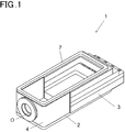
FIG. 1 is an overall perspective view of an electronic component accommodation package according to an embodiment of the present disclosure. -
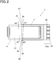
FIG. 2 is a top view of the electronic component accommodation package according to the embodiment of the present disclosure. -
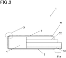
FIG. 3 is a side view of the electronic component accommodation package according to the embodiment of the present disclosure. -
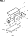
FIG. 4 is an exploded perspective side view of the electronic component accommodation package according to the embodiment of the present disclosure. -
FIG. 5 is an overall perspective view of an electronic device according to an embodiment of the present disclosure. -
FIG. 6 is an enlargement of X inFIG. 3 . - Hereinafter, an electronic
component accommodation package 1 and anelectronic device 10 according to an embodiment of the present invention will be described referring to the drawings. - First, the electronic component accommodation package 1 (hereinafter referred to as the package 1) will be described referring to
FIG. 1 to FIG. 4 andFIG. 6 . - The
package 1 is used for accommodating an element composed of a passive element. Such elements include, for example, active elements such as semiconductor elements, transistors, diodes and thyristors, resistors, capacitors, solar cells, piezoelectric elements, crystal oscillators, ceramic oscillators, and the like. More specifically, thepackage 1 is suitable for an element compatible with high voltage, large current, high speed and high frequency to be mounted therein to exhibit the function. As an example of the element, an electronic component such as a semiconductor element is mounted. Theelectronic device 10 is thepackage 1 with an electronic component such as a semiconductor element mounted therein as an example of the element. - The
package 1 includes asubstrate 2 and aframe 11. Theframe 11 includes afirst frame 3, asecond frame 4, and athird frame 7. Thefirst frame 3 is on theupper surface 24 of thesubstrate 2. Thesecond frame 4 is joined to thefirst frame 3. Thethird frame 7 is on the upper surface of thefirst frame 3 and the upper surface of thesecond frame 4. Thesecond frame 4 has a through hole O in a side wall. The through hole O penetrates the side wall outward from anmounting area 21 in a plan view. - The
substrate 2 has, for example, a rectangular shape in a plan view. As illustrated inFIG. 4 , theupper surface 24 of thesubstrate 2 includes amounting area 21 on which theelectronic component 5 is to be mounted and aperipheral area 22 surrounding themounting area 21. Thesubstrate 2 may be made of, for example, a metal material such as copper, iron, tungsten, molybdenum, nickel or cobalt, or an alloy containing any of these metal materials. Thesubstrate 2 may have a function of efficiently dissipating the heat generated in thepackage 1 by theelectronic component 5 to the outside of thepackage 1. Thesubstrate 2 may have good thermal conductivity. The thermal conductivity of thesubstrate 2 can be, for example, 15 W/(m·K) or more and 450 W/(m·K) or less. The coefficient of thermal expansion of thesubstrate 2 may be, for example, 3×10⁻⁶ /K or more and 28×10-6 /K or less. - The
substrate 2 is manufactured into a predetermined shape by applying metal working such as rolling or punching to an ingot that is obtained by casting a molten metal material into a mold and solidifying it. The length of each side of thesubstrate 2 in a plan view is, for example, 5 m or more and 50 mm or less. More specifically, as illustrated inFIG. 4 , thesubstrate 2 may have a rectangular shape with a first long side 2L1, a second long side 2L2, a first short side 2S1, and a second short side 2S2 in a plan view. In this case, the first long side 2L1 and the second long side 2L2 may be, for example, 10 mm or more and 50 mm or less, and the first short side 2S1 and the second short side 2S2 may be, for example, 5 mm or more and 20 mm or less. The thickness of thesubstrate 2 in the vertical direction (direction orthogonal to theupper surface 24 of the substrate 2) is, for example, 0.3 mm or more and 5 mm or less. - In order to prevent oxidative corrosion, a metal layer of nickel, gold or the like may be formed on the surface of the
substrate 2 by electroplating or electroless plating. The thickness of the metal layer is, for example, 0.5 µm or more and 9 µm or less. - The
frame 11 is on theupper surface 24 of thesubstrate 2 to surround themounting area 21. As described above, theframe 11 includes thefirst frame 3, thesecond frame 4, and thethird frame 7. Thefirst frame 3 is on theupper surface 24 of thesubstrate 2 along theperipheral area 22 of thesubstrate 2. Thefirst frame 3 may serve as an input/output terminal and can exchange signals between the internalelectronic component 5 and the outside. Thefirst frame 3 has, for example, a U shape in a plan view and may surround the inside from three directions. That is, thefirst frame 3 may be any member that is on theupper surface 24 of thesubstrate 2 to surround at least a part of themounting area 21. - As illustrated in
FIGS. 3 and4 , thefirst frame 3 may include a frame-shapedflat plate portion 31 and a frame-shaped wall portion 32 disposed on theflat plate portion 31. As illustrated inFIGS. 2 and3 , theflat plate portion 31 may have a protrudingportion 31a protruding outward from the outer edge of thesubstrate 2 in a plan view. In this regard, asignal wiring 33 may be disposed on the upper surface of the protrudingportion 31a. This allows thepackage 1 to be readily connected to an external electric circuit board via theprotruding portion 31a. The external electric circuit board may be, for example, a flexible board. - In the present embodiment, as illustrated in
FIG. 4 , the frame-shapedflat plate portion 31 of thefirst frame 3 includes a plate-shaped part in contact with thesubstrate 2 and a U-shaped frame part on the plate-shaped part. Even in this shape, thefirst frame 3 is disposed to surround at least a part of themounting area 21 of thesubstrate 2. - The
first frame 3 may include a metallized layer (not shown) that is on the under surface of theflat plate portion 31 and joined to thesubstrate 2, thesignal wiring 33 on the upper surface of theflat plate portion 31, a metal layer (not shown) on the upper surface of thewall portion 32, and aground layer 34 on the upper surfaces of theflat plate portion 31 and thewall portion 32. Thesignal wiring 33 is provided for electric conduction between the inside and outside of thepackage 1. Further, thesignal wiring 33 is a base for connecting a lead terminal or the like provided on the outside of thepackage 1. The metal layer is a base for joining thesecond frame 4, which will be described later, by a metal joining material such as a brazing material or solder. Theflat plate portion 31 has a rectangular shape in a plan view. Thewall portion 32 has a shape that is obtained by removing one side from a frame in a plan view. Theflat plate portion 31 and thewall portion 32 may be integrally formed in one piece. Alternatively, an insulating layer for further wiring a signal line may be provided between theflat plate portion 31 and thewall portion 32. Thefirst frame 3 can be freely and suitably configured according to the design of the signal wiring and the like of thepackage 1. Thefirst frame 3 contains a ceramic material. That is, theflat plate portion 31 and thewall portion 32 are made of an insulating material, for example a ceramic material such as an alumina-based sintered body, a mullite-based sintered body, a silicon carbide-based sintered body, an aluminum nitride-based sintered body, and a silicon nitride-based sintered body, or glass ceramics. Thesignal wiring 33 and the metal layer may be constituted by a base of a high-melting-point metal material such as tungsten, molybdenum or manganese and a plating layer of nickel, gold or the like formed thereon. The coefficient of thermal expansion of theflat plate portion 31 or thewall portion 32 containing a ceramic material is, for example, 3×10⁻⁶ /K or more and 8×10⁻⁶ /K or less. - A method of manufacturing the
first frame 3 will be described. On the upper surface, the under surface and the end surface opposed to the through hole O of the unsinteredflat plate portion 31 before being fired, a plurality ofsignal wirings 33 and theground layer 34 are formed along a side of the upper surface of theflat plate portion 31, for example, by screen printing. Further, on the upper surface of thewall portion 32 before being fired, the metal layer and theground layer 34 are formed by screen printing. Then, thewall portion 32, on which the unsintered metal layer andground layer 34 before being fired are formed, is pressure-bonded onto on theflat plate portion 31, on which the unsintered signal wirings 33 andground layer 34 before being fired are formed, and thewall portion 32 and theflat plate portion 31 are fired simultaneously. Thefirst frame 3 can be manufactured in this way. - In the fired
first frame 3 after firing, theflat plate portion 31 and thewall portion 32 are integrated in one piece. In a plan view of thefirst frame 3, eachsignal wiring 33 appears to be divided into two parts by thewall portion 32, but thesignal wiring 33 is continuous directly under thewall portion 32. Accordingly, in a plan view of thefirst frame 3, the part of eachsignal wiring 33 located inside thepackage 1 is electrically continuous with the part of thesignal wiring 33 located outside thepackage 1. This allows theelectronic component 5 in thepackage 1 to be connected to an electric circuit board outside thepackage 1 via thesignal wirings 33. - In a plan view, the length of each side of the
flat plate portion 31 is, for example, 3 mm or more and 50 mm or less. The height of theflat plate portion 31 is, for example, 1 mm or more and 10 mm or less. Further, in a plan view, the length of each side of thewall portion 32 is, for example, 1 mm or more and 50 mm or less. The height of thewall portion 32 is, for example, 1 mm or more and 10 mm or less. - Lead terminals (not shown) may be electrically connected on the signal wirings 33 via a brazing material. The lead terminals are provided for electric connection to an external electric circuit board or the like. By disposing the adjacent signal wirings 33 with a gap between them, the adjacent signal wirings 33 are electrically insulated from each other, and the electromagnetic coupling is also reduced.
- The
second frame 4 is joined to theupper surface 24 of thesubstrate 2 along theperipheral area 22 of thesubstrate 2 and is provided for protecting theelectronic component 5 from the outside as with thefirst frame 3. Thesecond frame 4 may have a frame shape, for example, formed in a U-shape in a plan view. Thesecond frame 4 may have a shape that surrounds the inside from three directions. That is, thesecond frame 4 may be any member that is on theupper surface 24 of thesubstrate 2 to surround at least a part of the mountingarea 21. Further, thesecond frame 4 may have the through hole O. For example, thesecond frame 4 is brazed to theupper surface 24 of thesubstrate 2 via a brazing material. This shape facilitates the processing of thesecond frame 4, for example, compared to asecond frame 4 that has a shape of surrounding all four sides and has an opening on a wall. As a result, the productivity can be improved. Further, also with regard to joining to thefirst frame 3, this shape can reduce the joining area, which can reduce mutual influence due to thermal deformation. - Further, the
second frame 4 contains a metal material. More specifically, thesecond frame 4 is made of, for example, a metal material such as copper, iron, tungsten, molybdenum, nickel or cobalt, or an alloy containing any of these metal materials. Thesecond frame 4 may have a function of efficiently dissipating the heat generated in the package by theelectronic component 5 1 to the outside of thepackage 1. The thermal conductivity of thesecond frame 4 is, for example, 15 W/(m·K) or more and 450 W/(m·K) or less. The coefficient of thermal expansion of thesecond frame 4 is, for example, 3×10⁻⁶ /K or more and 28×10-6 /K or less. - Further, as illustrated in
FIG. 2 , thesecond frame 4 may have a size that fits in thesubstrate 2 in a plan view. The length of the side of thesecond frame 4 along the short sides of thesubstrate 2 is, for example, 5 mm or more and 20 mm or less. The height of thesecond frame 4 is, for example, 5 mm or more and 20 mm or less. In a plan view of thesecond frame 4, the thickness of thesecond frame 4 is, for example, 0.5 mm or more and 3 mm or less. As used herein, the height of thesecond frame 4 refers to the size of thesecond frame 4 in the direction perpendicular to thesubstrate 2 inFIG. 3 . As will be described later, the thickness of thesecond frame 4 refers to the size of thesecond frame 4 in the direction perpendicular to the long sides or the short sides of thesubstrate 2 in a plan view as illustrated inFIG. 2 . The height and thickness of other frames can be defined in the same way. - Further, a lens or the like that transmits an optical signal may be provided to the
second frame 4 at a position where the through hole O is formed. For example, this allows an optical signal transmitted from the optical component mounted in thepackage 1 to be output to the outside. - As illustrated in
FIGS. 1 and2 , thethird frame 7 has a ring shape. Thethird frame 7 is on the upper surface of thefirst frame 3 and the upper surface of thesecond frame 4. Since thefirst frame 3 and thesecond frame 4 are located along theupper surface 24 of thesubstrate 2, the outer edge of thethird frame 7 may have the same shape as that of thesubstrate 2. Further, thethird frame 7 contains a metal material. For example, thethird frame 7 may be made of the same material as thesecond frame 4. In this case, the second frame and the third frame has the same coefficient of thermal expansion, which can reduce the risk of breakage due to thermal expansion at the joint surface between thesecond frame 4 and thethird frame 7. Thethird frame 7 is made of, for example, a metal material such as copper, iron, tungsten, molybdenum, nickel or cobalt, or an alloy containing any of these metal materials. - As illustrated in
FIGS. 2 and4 , thefirst frame 3 includes afirst end 3a and asecond end 3b, and thesecond frame 4 includes athird end 4a and afourth end 4b. Thefirst frame 3 and thesecond frame 4 are joined with each other via a joining material at the respective ends opposed to each other. More specifically, thefirst end 3a of thefirst frame 3 and thefourth end 4b of thesecond frame 4 are joined to each other via the joining material, and thesecond end 3b of thefirst frame 3 and thethird end 4a of thesecond frame 4 are joined to each other via the joining material. That is, thepackage 1 has such a shape that surrounds the mountingarea 21 from all four sides by thefirst frame 3 and thesecond frame 4. The joining material is a brazing material or the like. Then, thethird frame 7, which is another member, is disposed on the upper surface of thefirst frame 3 and the upper surface of thesecond frame 4 so as to surround the mountingarea 21. - In the present embodiment having the above-described configuration, the
first frame 3 and thesecond frame 4 are joined only at the respective ends in contrast to a configuration in which, for example, asecond frame 4 has cutouts to which the ends and the upper surfaces of afirst frame 3 are joined. This can reduce the joining area between thefirst frame 3 and thesecond frame 4. With the reduced joining area, it is possible to reduce the stress due to the difference in coefficient of thermal expansion and to reduce a load such as thermal stress that has an influence on both sides. Further, thefirst frame 3 and thesecond frame 4 may have a stepped shape. - In the present embodiment, the presence of the
third frame 7, which is a different member from thefirst frame 3 and thesecond frame 4, ensures the joining strength to thelid 6. Accordingly, even when thefirst frame 3 and thesecond frame 4 have different heights, it is possible to reduce the risk of the airtightness of theelectronic device 10 being impaired. - At the opposite ends where the
first frame 3 and thesecond frame 4 are joined to each other, thefirst frame 3 may be thicker than thesecond frame 4. That is, in a plan view as illustrated inFIG. 2 , the thickness w1 at thefirst end 3a of thefirst frame 3 may be greater than the thickness w4 at thefourth end 4b of thesecond frame 4, and the thickness w2 at thesecond end 3b of thefirst frame 3 may be greater than the thickness w3 at thethird end 4a of thesecond frame 4. As used herein, a thickness w refers to the width of a frame member in a plan view. More specifically, at opposite ends, a thickness w refers to the size of a frame member in a direction perpendicular to the long sides of thesubstrate 2 in a plan view. With this configuration, thepackage 1 can maintain the joining strength and the airtightness even when a misalignment between the joining surfaces of thefirst frame 3 and thesecond frame 4 occurs due to a positional error at the time of joining. As a result, the productivity of thepackage 1 with high airtightness is improved. - In the present embodiment, as illustrated in
FIG. 2 , the thickness of thefirst frame 3 and the thickness of the second frame are both constant over the entire length. That is, the thickness w1 of thefirst end 3a and the thickness w2 of thesecond end 3b are equal, and the thickness w3 of thethird end 4a and the thickness w4 of thefourth end 4b are equal. This configuration facilitates manufacture of the frame members. However the shape of each frame member is not limited to this, and any frame member may have a shape in which a certain part has a different thickness from the other part. - When the
substrate 2 has a rectangular shape, the position of the joint portion 8 between thefirst frame 3 and thesecond frame 4 may overlap the position of the long sides of thesubstrate 2. That is, in a plan view as illustrated inFIG. 2 andFIG. 4 , thesubstrate 2 has a rectangular shape with the first long side 2L1, the second long side 2L2, the first short side 2S1 and the second short side 2S2. In the plan view, a firstjoint portion 81, at which thefirst end 3a of thefirst frame 3 and thefourth end 4b of thesecond frame 4 are joined to each other, may overlap the first long side 2L1 of thesubstrate 2. Further, a secondjoint portion 82, at which thesecond end 3b of thefirst frame 3 and thethird end 4a of thesecond frame 4 are joined to each other, may overlap the second long side 2L2 of thesubstrate 2. With this configuration, it is possible to fix the long sides of thesubstrate 2, which tends to be deformed due to thermal stress, by the joining material or the like. This can reduce deformation of thesubstrate 2 due to thermal stress or the like. In this regard, the joint portion 8 is only preferred to be located substantially along the long sides of thesubstrate 2 and may be apart from the long sides within the range of production error or the like. - As illustrated in
FIG. 4 , the firstjoint portion 81 and the secondjoint portion 82 may be opposed to each other in a plan view. In this configuration, the firstjoint portion 81 and the secondjoint portion 82 are arranged at the same position on the respective long sides of thesubstrate 2. This can reduce the inclination and dimensional error of thepackage 1 caused by joining and improve the airtightness. - In a plan view, a part of the
first frame 3 is on the first short side 2S1 of thesubstrate 2, and a part of thesecond frame 4 is on the second short side 2S2 of thesubstrate 2. In this regard, the firstjoint portion 81 and the secondjoint portion 82 may be located closer to the first short side 2S1 than to the second short side 2S2 (not shown). This configuration increases the ratio of metal material in thepackage 1. This can increase the thermal conductivity of theentire package 1 and improve the heat dissipation property. In addition, the cost for thepackage 1 can be reduced. - As illustrated in
FIGS. 1 and2 , the outer edge of thefirst frame 3 may be located outside the outer edge of thethird frame 7 in a plan view. This configuration can reduce the risk of a crack being formed by a stress on an end (corner) of the joining surface at which thefirst frame 3 and thethird frame 7 are joined to each other. - As illustrated in
FIG. 6 , thethird frame 7 may have acurved surface 71 at the outer periphery at the portion joined to thefirst frame 3 and/or thesecond frame 4. That is, thethird frame 7 includes a third joint portion 83 (not shown) joined to thefirst frame 3 and a fourthjoint portion 84 joined to thesecond frame 4, and at least one of the third joint portion 83 and the fourthjoint portion 84 may have acurved surface 71 at the outer periphery. In this regard, thecurved surface 71 extends at least from the under surface of thethird frame 3 to the lateral surface of the outer periphery. This can disperse the thermal stress that is concentrically generated at the corners of the third frame 7and reduce the risk of breakage of thethird frame 7. Thecurved surface 71 may be provided either over the entire outer periphery of thefirst frame 3 and/or thesecond frame 4 or only at a part of the outer periphery. - In this regard, the
curved surface 71 may be located inside the outer edge of thefirst frame 3 in a plan view (seeFIG. 3 ). This configuration has both the effect of relaxing the thermal stress at the corners of thethird frame 7 and the effect of improving the joining strength by promoting the brazing material to form a fillet at the time of joining to thefirst frame 3. As a result, the airtightness can be further improved. - Next, the
electronic device 10 will be described referring toFIGS. 1 and5 . - As illustrated in
FIG. 1 , theelectronic device 10 can be manufactured by mounting theelectronic component 5 in thepackage 1. Theelectronic component 5 is electrically connected to the signal wirings 33 extended to the area surrounded by thesecond frame 4. Further, for example, by fixing an optical fiber to the lens provided at the through hole O of thepackage 1, it is possible to input/output an optical signal from the optical fiber into thepackage 1. - The
lid 6 has, for example, the same size as thesecond frame 4 in a plan view. Thelid 6 is joined to thethird frame 7 disposed on the upper surface of thesecond frame 4 and the upper surface of thefirst frame 3 by seam welding or via an adhesive such as solder. Thelid 6 is made of a metal material such as copper, iron, tungsten, molybdenum, nickel or cobalt. The thickness of thelid 6 is, for example, from 0.5 to 3 mm. By joining thelid 6 to the upper surface of thethird frame 7, the inner space surrounded by thepackage 1 and thelid 6 can be hermetically sealed. - Hereinafter, a method of manufacturing the
electronic device 10 illustrated inFIG. 5 will be described. First, thesubstrate 2, thefirst frame 3, and thesecond frame 4 are prepared. Each of thesubstrate 2 and thesecond frame 4 is manufactured into a predetermined shape by applying metal working to an ingot that is obtained by casting a molten metal material into a mold and solidifying it. - As for the
first frame 3, a ceramic green sheet to be theflat plate portion 31 and a ceramic green sheet die-cut corresponding to thewall portion 32 are prepared. Then, organic solvent containing molybdenum or manganese is applied to the ceramic green sheet to be theflat plate portion 31, for example, by screen printing so that the signal wirings 33 of metal paste are formed. Further, organic solvent containing molybdenum or manganese is applied to the ceramic green sheet to be thewall portion 32, for example, by screen printing so that the metal layer of metal paste is formed. Then, the ceramic green sheet to be thewall portion 32 is laminated on the ceramic green sheet to be theflat plate portion 31, and the laminate is sintered and cut into individual pieces having a desired shape. Thefirst frame 3 is thus formed. Furthermore, the metal layer is formed on the end surfaces (first end 3a andsecond end 3b) of thefirst frame 3 by screen printing, which become the joint surfaces with thesecond frame 4. Thefirst frame 3 can be manufactured in this way. Regarding the preparedsecond frame 4, a lens may be inserted in the through hole O of thesecond frame 4 and fixed by a brazing material. - Then, the
substrate 2, thefirst frame 3, and thesecond frame 4 thus prepared are joined together via a brazing material. In this step, pieces of the brazing material are placed respectively to portions of thesecond frame 4 to be joined to thesubstrate 2 and thefirst frame 3 beforehand. Thesecond frame 4, thesubstrate 2 and thefirst frame 3 are heated so that the brazing material spreads and wets the joint surfaces. Then, by cooling, thesecond frame 4, thesubstrate 2 and thefirst frame 3 are joined together. The electroniccomponent accommodation package 1 can be manufactured in this way. Further, theelectronic device 10 can be manufactured by mounting theelectronic component 5 or the like on the mountingarea 21 of the manufactured electroniccomponent accommodation package 1 with a joining material such as solder and covering the electroniccomponent accommodation package 1 by thelid 6. - The present invention is not limited to the above-described embodiment, and various modifications and improvements including those of numerical values can be made without departing from the features of the present invention. Further, the method of mounting the electronic component is not specified in the present embodiment.
-
- 1
- Electronic component accommodation package
- 2
- Substrate
- 21
- Mounting area
- 22
- Peripheral area
- 3
- First frame
3a First end
3b Second end - 31
- Flat plate portion
31a (Protruding portion) - 32
- wall portion
- 33
- Signal wiring
- 34
- Ground layer
- 4
- Second frame
4a Third end
4b Fourth end - 5
- Electronic component
- 6
- Lid
- 7
- Third frame
- 71
- Curved surface
- 8
- Joint portion
81 First joint portion
82 Second joint portion - 10
- Electronic device
- 11
- Frame
- O
- Through hole
- w1
- to w4 Thickness
Claims (12)
- An electronic component accommodation package, comprising:a substrate that has an upper surface including a mounting area on which an electronic component is to be mounted; anda frame that is on the upper surface of the substrate to surround the mounting area and that has a through hole penetrating the frame outward from the mounting area in a plan view,wherein the frame includes:a first frame that is on the upper surface of the substrate to surround at least a part of the mounting area and that contains a ceramic material;a second frame that is on the upper surface of the substrate to surround at least a part of the mounting area, that has the through hole and that contains a metal material; anda third frame that is on an upper surface of the first frame and an upper surface of the second frame to surround the mounting area in the plan view and that contains a metal material,wherein the first frame includes a first end and a second end, and the second frame includes a third end and a fourth end, andwherein the first end of the first frame and the fourth end of the second frame are joined to each other via a joining material, and the second end of the first frame and the third end of the second frame are joined to each other via a joining material.
- The electronic component accommodation package according to claim 1, wherein a material of the second frame is same as a material of the third frame.
- The electronic component accommodation package according to claim 1 or 2, wherein in the plan view, the second frame has a U-shape along a part of an outer edge of the substrate.
- The electronic component accommodation package according to any one of claims 1 to 3, wherein in the plan view, a thickness of the first end of the first frame is greater than a thickness of the fourth end of the second frame, and a thickness of the second end of the first frame is greater than a thickness of the third end of the second frame.
- The electronic component accommodation package according to any one of claims 1 to 4,wherein in the plan view, the substrate has a rectangular shape with a first long side, a second long side, a first short side, and a second short side, andwherein in the plan view, a first joint portion overlaps the first long side of the substrate, and a second joint portion overlaps the second long side of the substrate, the first joint portion being a portion at which the first end of the first frame and the fourth end of the second frame being joined to each other, the second joint portion being a portion at which the second end of the first frame and the third end of the second frame being joined to each other.
- The electronic component accommodation package according to claim 5, wherein in the plan view, the first joint portion and the second joint portion are opposed to each other.
- The electronic component accommodation package according to claim 5 or 6,wherein in the plan view, a part of the first frame is on the first short side of the substrate, and a part of the second frame is on the second short side of the substrate, andwherein in the plan view, the first joint portion and the second joint portion are closer to the first short side than to the second short side.
- The electronic component accommodation package according to any one of claims 1 to 7, wherein in the plan view, an outer edge of the first frame is located outside an outer edge of the third frame.
- The electronic component accommodation package according to any one of claims 1 to 8,wherein the third frame includes a third joint portion joined to the upper surface of the first frame, and a fourth joint portion joined to the upper surface of the second frame, andwherein at least one of the third joint portion and the fourth joint portion has a curved surface at an outer periphery.
- The electronic component accommodation package according to claim 9,wherein the third joint portion has the curved surface at the outer periphery, andwherein in the plan view, the curved surface is located inside an outer edge of the first frame.
- The electronic component accommodation package according to any one of claims 1 to 10,wherein the first frame includes a protruding portion that protrudes outward from an outer edge of the substrate in the plan view, andwherein a signal wiring is provided on an upper surface of the protruding portion.
- An electronic device, comprising:the electronic component accommodation package according to any one of claims 1 to 11;an electronic component mounted on the mounting area; anda lid that covers the electronic component and that is bonded on an upper surface of the third frame via an adhesive.
Applications Claiming Priority (2)
| Application Number | Priority Date | Filing Date | Title |
|---|---|---|---|
| JP2018203588 | 2018-10-30 | ||
| PCT/JP2019/042567 WO2020090882A1 (en) | 2018-10-30 | 2019-10-30 | Package for containing electronic component, and electronic device |
Publications (2)
| Publication Number | Publication Date |
|---|---|
| EP3876272A1 true EP3876272A1 (en) | 2021-09-08 |
| EP3876272A4 EP3876272A4 (en) | 2022-08-17 |
Family
ID=70463702
Family Applications (1)
| Application Number | Title | Priority Date | Filing Date |
|---|---|---|---|
| EP19878889.5A Withdrawn EP3876272A4 (en) | 2018-10-30 | 2019-10-30 | HOUSING FOR CONTAINING AN ELECTRONIC COMPONENT AND ELECTRONIC DEVICE |
Country Status (5)
| Country | Link |
|---|---|
| US (1) | US12387990B2 (en) |
| EP (1) | EP3876272A4 (en) |
| JP (1) | JP7160940B2 (en) |
| CN (1) | CN112956015B (en) |
| WO (1) | WO2020090882A1 (en) |
Families Citing this family (1)
| Publication number | Priority date | Publication date | Assignee | Title |
|---|---|---|---|---|
| US20240105528A1 (en) * | 2021-01-29 | 2024-03-28 | Kyocera Corporation | Semiconductor package and semiconductor electronic device |
Family Cites Families (23)
| Publication number | Priority date | Publication date | Assignee | Title |
|---|---|---|---|---|
| JP3012091B2 (en) * | 1992-06-08 | 2000-02-21 | 日本特殊陶業株式会社 | Seal ring and manufacturing method thereof |
| JPH1117041A (en) * | 1997-06-20 | 1999-01-22 | Sumitomo Electric Ind Ltd | Optical semiconductor package |
| JP4794074B2 (en) * | 2001-06-28 | 2011-10-12 | 京セラ株式会社 | Semiconductor element storage package and semiconductor device |
| JP2003133451A (en) * | 2001-10-22 | 2003-05-09 | Sumitomo Metal Electronics Devices Inc | Package for optical communication |
| JP2004266188A (en) * | 2003-03-04 | 2004-09-24 | Matsushita Electric Ind Co Ltd | Semiconductor device package, method of manufacturing the same, and semiconductor device using the same |
| US6992250B2 (en) * | 2004-02-26 | 2006-01-31 | Kyocera Corporation | Electronic component housing package and electronic apparatus |
| JP2007273852A (en) * | 2006-03-31 | 2007-10-18 | Ngk Spark Plug Co Ltd | Light emitting element storage package |
| JP2008235531A (en) * | 2007-03-20 | 2008-10-02 | Mitsubishi Electric Corp | Hermetically sealed package and connection structure |
| JP2010062181A (en) | 2008-09-01 | 2010-03-18 | Sumitomo Metal Electronics Devices Inc | Package for storing electronic component |
| WO2010150729A1 (en) * | 2009-06-26 | 2010-12-29 | 京セラ株式会社 | Element storage package and mounting structure |
| JP5773851B2 (en) * | 2011-11-28 | 2015-09-02 | 京セラ株式会社 | Electronic component storage package and electronic device |
| JP5823023B2 (en) * | 2012-03-22 | 2015-11-25 | 京セラ株式会社 | Device storage package |
| JP5826113B2 (en) * | 2012-05-24 | 2015-12-02 | 京セラ株式会社 | Piezoelectric vibration element storage package, piezoelectric device, and multi-piece wiring board |
| JP5873174B2 (en) * | 2012-07-27 | 2016-03-01 | 京セラ株式会社 | Semiconductor element storage package and semiconductor device |
| JP5969317B2 (en) * | 2012-08-24 | 2016-08-17 | 京セラ株式会社 | Optical semiconductor element storage package and mounting structure |
| CN104364897B (en) * | 2012-10-29 | 2017-07-25 | 京瓷株式会社 | Element storage packaging part and assembling structure |
| JP5898332B2 (en) * | 2012-10-30 | 2016-04-06 | 京セラ株式会社 | Electronic component storage container and electronic device |
| JP2014127589A (en) * | 2012-12-26 | 2014-07-07 | Kyocera Corp | Package for housing element and mounting structure |
| JP5981660B2 (en) * | 2013-09-25 | 2016-08-31 | 京セラ株式会社 | Electronic component storage package and electronic device |
| JP6239999B2 (en) * | 2014-02-25 | 2017-11-29 | 京セラ株式会社 | Electronic component storage package and electronic device |
| JP6272140B2 (en) * | 2014-05-26 | 2018-01-31 | 京セラ株式会社 | Semiconductor element storage package and semiconductor device including the same |
| JP2016086126A (en) * | 2014-10-28 | 2016-05-19 | 京セラ株式会社 | Semiconductor element package and semiconductor device |
| JP6725408B2 (en) * | 2016-12-22 | 2020-07-15 | 京セラ株式会社 | Electronic component storage package and electronic device |
-
2019
- 2019-10-30 EP EP19878889.5A patent/EP3876272A4/en not_active Withdrawn
- 2019-10-30 US US17/288,951 patent/US12387990B2/en active Active
- 2019-10-30 CN CN201980071157.4A patent/CN112956015B/en active Active
- 2019-10-30 WO PCT/JP2019/042567 patent/WO2020090882A1/en not_active Ceased
- 2019-10-30 JP JP2020553975A patent/JP7160940B2/en active Active
Also Published As
| Publication number | Publication date |
|---|---|
| US12387990B2 (en) | 2025-08-12 |
| CN112956015B (en) | 2024-05-24 |
| EP3876272A4 (en) | 2022-08-17 |
| US20210398866A1 (en) | 2021-12-23 |
| WO2020090882A1 (en) | 2020-05-07 |
| JP7160940B2 (en) | 2022-10-25 |
| JPWO2020090882A1 (en) | 2021-09-02 |
| CN112956015A (en) | 2021-06-11 |
Similar Documents
| Publication | Publication Date | Title |
|---|---|---|
| CN102884618B (en) | Element housing package, and electronic device using the same | |
| US11776929B2 (en) | Semiconductor device and lead frame member | |
| JP5873174B2 (en) | Semiconductor element storage package and semiconductor device | |
| CN104126224A (en) | Packages for Component Storage | |
| KR102425194B1 (en) | Package | |
| US12387990B2 (en) | Electronic component accommodation package and electronic device | |
| JP6075597B2 (en) | Device storage package and mounting structure | |
| CN110476245B (en) | module | |
| JP6496622B2 (en) | Ceramic wiring board and electronic component storage package | |
| CN105164801B (en) | Element storage packaging part and the assembling structure for possessing it | |
| JP6030371B2 (en) | Device storage package and mounting structure | |
| JP5905728B2 (en) | Device storage package and mounting structure | |
| JP5213663B2 (en) | Electronic device mounting structure | |
| JP6760788B2 (en) | Semiconductor packages and semiconductor devices | |
| JP5992785B2 (en) | Semiconductor element storage package and semiconductor device | |
| JP7196249B2 (en) | Packages for semiconductor devices and semiconductor devices | |
| JP6698492B2 (en) | Semiconductor package and semiconductor device | |
| JP2007242908A (en) | Ceramic package for electronic component storage | |
| JP2003318305A (en) | High frequency package | |
| JP2012134301A (en) | Wiring board |
Legal Events
| Date | Code | Title | Description |
|---|---|---|---|
| STAA | Information on the status of an ep patent application or granted ep patent |
Free format text: STATUS: THE INTERNATIONAL PUBLICATION HAS BEEN MADE |
|
| PUAI | Public reference made under article 153(3) epc to a published international application that has entered the european phase |
Free format text: ORIGINAL CODE: 0009012 |
|
| STAA | Information on the status of an ep patent application or granted ep patent |
Free format text: STATUS: REQUEST FOR EXAMINATION WAS MADE |
|
| 17P | Request for examination filed |
Effective date: 20210427 |
|
| AK | Designated contracting states |
Kind code of ref document: A1 Designated state(s): AL AT BE BG CH CY CZ DE DK EE ES FI FR GB GR HR HU IE IS IT LI LT LU LV MC MK MT NL NO PL PT RO RS SE SI SK SM TR |
|
| DAV | Request for validation of the european patent (deleted) | ||
| DAX | Request for extension of the european patent (deleted) | ||
| REG | Reference to a national code |
Ref country code: DE Ref legal event code: R079 Free format text: PREVIOUS MAIN CLASS: H01L0023080000 Ipc: H01L0023040000 |
|
| A4 | Supplementary search report drawn up and despatched |
Effective date: 20220720 |
|
| RIC1 | Information provided on ipc code assigned before grant |
Ipc: H01L 23/00 20060101ALI20220714BHEP Ipc: H01L 23/10 20060101ALI20220714BHEP Ipc: H01L 23/04 20060101AFI20220714BHEP |
|
| P01 | Opt-out of the competence of the unified patent court (upc) registered |
Effective date: 20230505 |
|
| STAA | Information on the status of an ep patent application or granted ep patent |
Free format text: STATUS: THE APPLICATION HAS BEEN WITHDRAWN |
|
| 18W | Application withdrawn |
Effective date: 20250723 |