EP3869556A1 - Stacked semiconductor die assemblies with support members and associated systems and methods - Google Patents
Stacked semiconductor die assemblies with support members and associated systems and methods Download PDFInfo
- Publication number
- EP3869556A1 EP3869556A1 EP20216842.3A EP20216842A EP3869556A1 EP 3869556 A1 EP3869556 A1 EP 3869556A1 EP 20216842 A EP20216842 A EP 20216842A EP 3869556 A1 EP3869556 A1 EP 3869556A1
- Authority
- EP
- European Patent Office
- Prior art keywords
- die
- memory
- package substrate
- attaching
- support members
- Prior art date
- Legal status (The legal status is an assumption and is not a legal conclusion. Google has not performed a legal analysis and makes no representation as to the accuracy of the status listed.)
- Pending
Links
Images





Classifications
-
- H—ELECTRICITY
- H10—SEMICONDUCTOR DEVICES; ELECTRIC SOLID-STATE DEVICES NOT OTHERWISE PROVIDED FOR
- H10W—GENERIC PACKAGES, INTERCONNECTIONS, CONNECTORS OR OTHER CONSTRUCTIONAL DETAILS OF DEVICES COVERED BY CLASS H10
- H10W90/00—Package configurations
-
- H—ELECTRICITY
- H10—SEMICONDUCTOR DEVICES; ELECTRIC SOLID-STATE DEVICES NOT OTHERWISE PROVIDED FOR
- H10W—GENERIC PACKAGES, INTERCONNECTIONS, CONNECTORS OR OTHER CONSTRUCTIONAL DETAILS OF DEVICES COVERED BY CLASS H10
- H10W72/00—Interconnections or connectors in packages
- H10W72/30—Die-attach connectors
-
- H—ELECTRICITY
- H10—SEMICONDUCTOR DEVICES; ELECTRIC SOLID-STATE DEVICES NOT OTHERWISE PROVIDED FOR
- H10W—GENERIC PACKAGES, INTERCONNECTIONS, CONNECTORS OR OTHER CONSTRUCTIONAL DETAILS OF DEVICES COVERED BY CLASS H10
- H10W72/00—Interconnections or connectors in packages
- H10W72/50—Bond wires
-
- H—ELECTRICITY
- H10—SEMICONDUCTOR DEVICES; ELECTRIC SOLID-STATE DEVICES NOT OTHERWISE PROVIDED FOR
- H10W—GENERIC PACKAGES, INTERCONNECTIONS, CONNECTORS OR OTHER CONSTRUCTIONAL DETAILS OF DEVICES COVERED BY CLASS H10
- H10W74/00—Encapsulations, e.g. protective coatings
- H10W74/10—Encapsulations, e.g. protective coatings characterised by their shape or disposition
- H10W74/111—Encapsulations, e.g. protective coatings characterised by their shape or disposition the semiconductor body being completely enclosed
- H10W74/114—Encapsulations, e.g. protective coatings characterised by their shape or disposition the semiconductor body being completely enclosed by a substrate and the encapsulations
- H10W74/117—Encapsulations, e.g. protective coatings characterised by their shape or disposition the semiconductor body being completely enclosed by a substrate and the encapsulations the substrate having spherical bumps for external connection
-
- H—ELECTRICITY
- H10—SEMICONDUCTOR DEVICES; ELECTRIC SOLID-STATE DEVICES NOT OTHERWISE PROVIDED FOR
- H10W—GENERIC PACKAGES, INTERCONNECTIONS, CONNECTORS OR OTHER CONSTRUCTIONAL DETAILS OF DEVICES COVERED BY CLASS H10
- H10W46/00—Marks applied to devices, e.g. for alignment or identification
-
- H—ELECTRICITY
- H10—SEMICONDUCTOR DEVICES; ELECTRIC SOLID-STATE DEVICES NOT OTHERWISE PROVIDED FOR
- H10W—GENERIC PACKAGES, INTERCONNECTIONS, CONNECTORS OR OTHER CONSTRUCTIONAL DETAILS OF DEVICES COVERED BY CLASS H10
- H10W70/00—Package substrates; Interposers; Redistribution layers [RDL]
- H10W70/60—Insulating or insulated package substrates; Interposers; Redistribution layers
- H10W70/62—Insulating or insulated package substrates; Interposers; Redistribution layers characterised by their interconnections
- H10W70/65—Shapes or dispositions of interconnections
- H10W70/654—Top-view layouts
- H10W70/655—Fan-out layouts
-
- H—ELECTRICITY
- H10—SEMICONDUCTOR DEVICES; ELECTRIC SOLID-STATE DEVICES NOT OTHERWISE PROVIDED FOR
- H10W—GENERIC PACKAGES, INTERCONNECTIONS, CONNECTORS OR OTHER CONSTRUCTIONAL DETAILS OF DEVICES COVERED BY CLASS H10
- H10W70/00—Package substrates; Interposers; Redistribution layers [RDL]
- H10W70/60—Insulating or insulated package substrates; Interposers; Redistribution layers
- H10W70/62—Insulating or insulated package substrates; Interposers; Redistribution layers characterised by their interconnections
- H10W70/65—Shapes or dispositions of interconnections
- H10W70/654—Top-view layouts
- H10W70/656—Fan-in layouts
-
- H—ELECTRICITY
- H10—SEMICONDUCTOR DEVICES; ELECTRIC SOLID-STATE DEVICES NOT OTHERWISE PROVIDED FOR
- H10W—GENERIC PACKAGES, INTERCONNECTIONS, CONNECTORS OR OTHER CONSTRUCTIONAL DETAILS OF DEVICES COVERED BY CLASS H10
- H10W72/00—Interconnections or connectors in packages
- H10W72/071—Connecting or disconnecting
- H10W72/073—Connecting or disconnecting of die-attach connectors
-
- H—ELECTRICITY
- H10—SEMICONDUCTOR DEVICES; ELECTRIC SOLID-STATE DEVICES NOT OTHERWISE PROVIDED FOR
- H10W—GENERIC PACKAGES, INTERCONNECTIONS, CONNECTORS OR OTHER CONSTRUCTIONAL DETAILS OF DEVICES COVERED BY CLASS H10
- H10W72/00—Interconnections or connectors in packages
- H10W72/071—Connecting or disconnecting
- H10W72/073—Connecting or disconnecting of die-attach connectors
- H10W72/07331—Connecting techniques
- H10W72/07332—Compression bonding, e.g. thermocompression bonding
-
- H—ELECTRICITY
- H10—SEMICONDUCTOR DEVICES; ELECTRIC SOLID-STATE DEVICES NOT OTHERWISE PROVIDED FOR
- H10W—GENERIC PACKAGES, INTERCONNECTIONS, CONNECTORS OR OTHER CONSTRUCTIONAL DETAILS OF DEVICES COVERED BY CLASS H10
- H10W72/00—Interconnections or connectors in packages
- H10W72/071—Connecting or disconnecting
- H10W72/073—Connecting or disconnecting of die-attach connectors
- H10W72/07331—Connecting techniques
- H10W72/07337—Connecting techniques using a polymer adhesive, e.g. an adhesive based on silicone or epoxy
-
- H—ELECTRICITY
- H10—SEMICONDUCTOR DEVICES; ELECTRIC SOLID-STATE DEVICES NOT OTHERWISE PROVIDED FOR
- H10W—GENERIC PACKAGES, INTERCONNECTIONS, CONNECTORS OR OTHER CONSTRUCTIONAL DETAILS OF DEVICES COVERED BY CLASS H10
- H10W72/00—Interconnections or connectors in packages
- H10W72/071—Connecting or disconnecting
- H10W72/073—Connecting or disconnecting of die-attach connectors
- H10W72/07331—Connecting techniques
- H10W72/07337—Connecting techniques using a polymer adhesive, e.g. an adhesive based on silicone or epoxy
- H10W72/07338—Connecting techniques using a polymer adhesive, e.g. an adhesive based on silicone or epoxy hardening the adhesive by curing, e.g. thermosetting
-
- H—ELECTRICITY
- H10—SEMICONDUCTOR DEVICES; ELECTRIC SOLID-STATE DEVICES NOT OTHERWISE PROVIDED FOR
- H10W—GENERIC PACKAGES, INTERCONNECTIONS, CONNECTORS OR OTHER CONSTRUCTIONAL DETAILS OF DEVICES COVERED BY CLASS H10
- H10W72/00—Interconnections or connectors in packages
- H10W72/071—Connecting or disconnecting
- H10W72/073—Connecting or disconnecting of die-attach connectors
- H10W72/07351—Connecting or disconnecting of die-attach connectors characterised by changes in properties of the die-attach connectors during connecting
- H10W72/07354—Connecting or disconnecting of die-attach connectors characterised by changes in properties of the die-attach connectors during connecting changes in dispositions
-
- H—ELECTRICITY
- H10—SEMICONDUCTOR DEVICES; ELECTRIC SOLID-STATE DEVICES NOT OTHERWISE PROVIDED FOR
- H10W—GENERIC PACKAGES, INTERCONNECTIONS, CONNECTORS OR OTHER CONSTRUCTIONAL DETAILS OF DEVICES COVERED BY CLASS H10
- H10W72/00—Interconnections or connectors in packages
- H10W72/071—Connecting or disconnecting
- H10W72/075—Connecting or disconnecting of bond wires
-
- H—ELECTRICITY
- H10—SEMICONDUCTOR DEVICES; ELECTRIC SOLID-STATE DEVICES NOT OTHERWISE PROVIDED FOR
- H10W—GENERIC PACKAGES, INTERCONNECTIONS, CONNECTORS OR OTHER CONSTRUCTIONAL DETAILS OF DEVICES COVERED BY CLASS H10
- H10W72/00—Interconnections or connectors in packages
- H10W72/30—Die-attach connectors
- H10W72/341—Dispositions of die-attach connectors, e.g. layouts
- H10W72/347—Dispositions of multiple die-attach connectors
-
- H—ELECTRICITY
- H10—SEMICONDUCTOR DEVICES; ELECTRIC SOLID-STATE DEVICES NOT OTHERWISE PROVIDED FOR
- H10W—GENERIC PACKAGES, INTERCONNECTIONS, CONNECTORS OR OTHER CONSTRUCTIONAL DETAILS OF DEVICES COVERED BY CLASS H10
- H10W72/00—Interconnections or connectors in packages
- H10W72/50—Bond wires
- H10W72/541—Dispositions of bond wires
- H10W72/5449—Dispositions of bond wires not being orthogonal to a side surface of the chip, e.g. fan-out arrangements
-
- H—ELECTRICITY
- H10—SEMICONDUCTOR DEVICES; ELECTRIC SOLID-STATE DEVICES NOT OTHERWISE PROVIDED FOR
- H10W—GENERIC PACKAGES, INTERCONNECTIONS, CONNECTORS OR OTHER CONSTRUCTIONAL DETAILS OF DEVICES COVERED BY CLASS H10
- H10W72/00—Interconnections or connectors in packages
- H10W72/50—Bond wires
- H10W72/59—Bond pads specially adapted therefor
-
- H—ELECTRICITY
- H10—SEMICONDUCTOR DEVICES; ELECTRIC SOLID-STATE DEVICES NOT OTHERWISE PROVIDED FOR
- H10W—GENERIC PACKAGES, INTERCONNECTIONS, CONNECTORS OR OTHER CONSTRUCTIONAL DETAILS OF DEVICES COVERED BY CLASS H10
- H10W72/00—Interconnections or connectors in packages
- H10W72/851—Dispositions of multiple connectors or interconnections
- H10W72/874—On different surfaces
- H10W72/884—Die-attach connectors and bond wires
-
- H—ELECTRICITY
- H10—SEMICONDUCTOR DEVICES; ELECTRIC SOLID-STATE DEVICES NOT OTHERWISE PROVIDED FOR
- H10W—GENERIC PACKAGES, INTERCONNECTIONS, CONNECTORS OR OTHER CONSTRUCTIONAL DETAILS OF DEVICES COVERED BY CLASS H10
- H10W72/00—Interconnections or connectors in packages
- H10W72/90—Bond pads, in general
- H10W72/931—Shapes of bond pads
- H10W72/932—Plan-view shape, i.e. in top view
-
- H—ELECTRICITY
- H10—SEMICONDUCTOR DEVICES; ELECTRIC SOLID-STATE DEVICES NOT OTHERWISE PROVIDED FOR
- H10W—GENERIC PACKAGES, INTERCONNECTIONS, CONNECTORS OR OTHER CONSTRUCTIONAL DETAILS OF DEVICES COVERED BY CLASS H10
- H10W72/00—Interconnections or connectors in packages
- H10W72/90—Bond pads, in general
- H10W72/941—Dispositions of bond pads
- H10W72/944—Dispositions of multiple bond pads
- H10W72/9445—Top-view layouts, e.g. mirror arrays
-
- H—ELECTRICITY
- H10—SEMICONDUCTOR DEVICES; ELECTRIC SOLID-STATE DEVICES NOT OTHERWISE PROVIDED FOR
- H10W—GENERIC PACKAGES, INTERCONNECTIONS, CONNECTORS OR OTHER CONSTRUCTIONAL DETAILS OF DEVICES COVERED BY CLASS H10
- H10W72/00—Interconnections or connectors in packages
- H10W72/90—Bond pads, in general
- H10W72/951—Materials of bond pads
-
- H—ELECTRICITY
- H10—SEMICONDUCTOR DEVICES; ELECTRIC SOLID-STATE DEVICES NOT OTHERWISE PROVIDED FOR
- H10W—GENERIC PACKAGES, INTERCONNECTIONS, CONNECTORS OR OTHER CONSTRUCTIONAL DETAILS OF DEVICES COVERED BY CLASS H10
- H10W74/00—Encapsulations, e.g. protective coatings
-
- H—ELECTRICITY
- H10—SEMICONDUCTOR DEVICES; ELECTRIC SOLID-STATE DEVICES NOT OTHERWISE PROVIDED FOR
- H10W—GENERIC PACKAGES, INTERCONNECTIONS, CONNECTORS OR OTHER CONSTRUCTIONAL DETAILS OF DEVICES COVERED BY CLASS H10
- H10W90/00—Package configurations
- H10W90/20—Configurations of stacked chips
-
- H—ELECTRICITY
- H10—SEMICONDUCTOR DEVICES; ELECTRIC SOLID-STATE DEVICES NOT OTHERWISE PROVIDED FOR
- H10W—GENERIC PACKAGES, INTERCONNECTIONS, CONNECTORS OR OTHER CONSTRUCTIONAL DETAILS OF DEVICES COVERED BY CLASS H10
- H10W90/00—Package configurations
- H10W90/20—Configurations of stacked chips
- H10W90/24—Configurations of stacked chips at least one of the stacked chips being laterally offset from a neighbouring stacked chip, e.g. chip stacks having a staircase shape
-
- H—ELECTRICITY
- H10—SEMICONDUCTOR DEVICES; ELECTRIC SOLID-STATE DEVICES NOT OTHERWISE PROVIDED FOR
- H10W—GENERIC PACKAGES, INTERCONNECTIONS, CONNECTORS OR OTHER CONSTRUCTIONAL DETAILS OF DEVICES COVERED BY CLASS H10
- H10W90/00—Package configurations
- H10W90/701—Package configurations characterised by the relative positions of pads or connectors relative to package parts
- H10W90/731—Package configurations characterised by the relative positions of pads or connectors relative to package parts of die-attach connectors
- H10W90/732—Package configurations characterised by the relative positions of pads or connectors relative to package parts of die-attach connectors between stacked chips
-
- H—ELECTRICITY
- H10—SEMICONDUCTOR DEVICES; ELECTRIC SOLID-STATE DEVICES NOT OTHERWISE PROVIDED FOR
- H10W—GENERIC PACKAGES, INTERCONNECTIONS, CONNECTORS OR OTHER CONSTRUCTIONAL DETAILS OF DEVICES COVERED BY CLASS H10
- H10W90/00—Package configurations
- H10W90/701—Package configurations characterised by the relative positions of pads or connectors relative to package parts
- H10W90/731—Package configurations characterised by the relative positions of pads or connectors relative to package parts of die-attach connectors
- H10W90/734—Package configurations characterised by the relative positions of pads or connectors relative to package parts of die-attach connectors between a chip and a stacked insulating package substrate, interposer or RDL
-
- H—ELECTRICITY
- H10—SEMICONDUCTOR DEVICES; ELECTRIC SOLID-STATE DEVICES NOT OTHERWISE PROVIDED FOR
- H10W—GENERIC PACKAGES, INTERCONNECTIONS, CONNECTORS OR OTHER CONSTRUCTIONAL DETAILS OF DEVICES COVERED BY CLASS H10
- H10W90/00—Package configurations
- H10W90/701—Package configurations characterised by the relative positions of pads or connectors relative to package parts
- H10W90/751—Package configurations characterised by the relative positions of pads or connectors relative to package parts of bond wires
- H10W90/754—Package configurations characterised by the relative positions of pads or connectors relative to package parts of bond wires between a chip and a stacked insulating package substrate, interposer or RDL
Definitions
- the disclosed embodiments relate to semiconductor die assemblies and to support members in such assemblies.
- the present technology relates to die assemblies that can include a controller die and memory dies carried above the controller die.
- Packaged semiconductor dies including memory chips, microprocessor chips, and imager chips, can include semiconductor dies mounted on a package substrate.
- the semiconductor dies are encased in a plastic protective covering, and each die includes functional features, such as memory cells, processor circuits, and imager devices. Bond pads on the dies are electrically connected between the functional features and terminals on the package substrate that allow the dies to be connected to external circuitry.
- the dies can be stacked upon one another within the casing.
- One challenge with vertically stacked dies is that the dies can have different sizes or footprints.
- a memory controller die can have a smaller footprint than the memory dies within the package.
- the memory controller die can be more difficult to wirebond because it is offset from the memory dies.
- the memory dies can sometimes tilt when stacked upon the smaller memory controller die.
- semiconductor die generally refers to a die having integrated circuits or components, data storage elements, processing components, and/or other features manufactured on semiconductor substrates.
- semiconductor dies can include integrated circuit memory and/or logic circuitry.
- Semiconductor dies and/or other features in semiconductor die packages can be said to be in "thermal contact" with one another if the two structures can exchange energy through heat.
- the terms “vertical,” “lateral,” “upper” and “lower” can refer to relative directions or positions of features in the semiconductor die assemblies in view of the orientation shown in the Figures. For example, “upper” or “uppermost” can refer to a feature positioned closer to the top of a page than another feature. These terms, however, should be construed broadly to include semiconductor devices having other orientations, such as being flipped on their side or inverted.
- Figure 1A is a cross-sectional view of a semiconductor die assembly 100 (“assembly 100") configured in accordance with an embodiment of the present technology.
- the assembly 100 includes a package substrate 102 carrying a first semiconductor die, or controller die 103, and first and second support members 130a and 130b (collectively “support members 130") on opposite sides of the controller die 103.
- the support members 130 carry first and second semiconductor dies, or first and second memory dies 106a and 106b (collectively “memory dies 106”), arranged in a stack above the controller die 103.
- the package substrate 102 includes a plurality of first bond pads 108a within the footprint (e.g., directly beneath) the first memory die 106a and a plurality of second bond pads 108b outside of the footprint (e.g., not directly beneath) the first memory die 106a.
- the first bond pads 108a are coupled to corresponding bond pads 109a on the controller die 103 by first wire bonds 111a
- the second bond pads 108b are coupled to corresponding bond pads 109b on each of the memory dies 106 by second wire bonds 111b.
- the package substrate 102 can include, for example, a printed circuit board or other suitable substrate having electrical connectors 104 (shown schematically), such as metal traces, vias, or other suitable connectors.
- the electrical connectors 104 can couple the first bond pads 108a and/or the second bond pads 108b to external circuitry (not shown) via package contacts 113 and interconnects 114 (e.g., bump bonds) at the opposite side of the package substrate 102.
- the electrical connectors 104 can also couple individual first bond pads 108a with individual second bond pads 108b to electrically intercouple the controller die 103 with the memory dies 106.
- the assembly 100 further includes a package casing 115 composed of an encapsulant 116 that at least partially encapsulates the controller die 103, the memory dies 106, and the support members 130.
- the encapsulant 116 also extends into a cavity 118 between the package substrate 102 and the first memory die 106a to at least partially fill the region beneath the first memory die 106a not occupied by the controller die 103 and the support members.
- the portion of the encapsulant 116 in the cavity 118 can reinforce the support members 130 and provide further mechanical support beneath the first memory die 106a.
- the encapsulant 116 can include, for example, a thermoset material, an epoxy resin, or other suitable compound that provides mechanical support, shielding from the ambient environment (e.g., from humidity), and/or electrical isolation (e.g., between wire bonds).
- the controller die 103 and the memory dies 106 can each be formed from a semiconductor substrate, such as silicon, silicon-on-insulator, compound semiconductor (e.g., Gallium Nitride), or other suitable substrate.
- the semiconductor substrate can be cut or singulated into semiconductor dies having any of variety of integrate circuit components or functional features, such as dynamic random-access memory (DRAM), static random-access memory (SRAM), flash memory, other forms of integrated circuit devices, including memory, processing circuits, imaging components, and/or other semiconductor devices.
- the assembly 100 can be configured as a memory in which the memory dies 106 provide data storage (e.g., NAND dies) and the controller die 103 provides memory control (e.g., NAND control).
- the assembly 100 can include other semiconductor dies in addition to and/or in lieu of one or more of the controller die 103 and/or the memory dies 106.
- the assembly 100 can include more than two memory dies (e.g., four dies, eight dies, etc.) or only a single memory die.
- the dies of the assembly 100 can have different sizes.
- one or both of the memory dies 106 can extend beyond the support members 130 at one or more sides.
- the controller die 103 is attached to the package substrate 102 by a die-attach material 140 (e.g., a die-attach film).
- the first support member 130a is attached to the package substrate 102 by a die-attach material 141a
- the second support member 130b is attached to the package substrate 102 by a die-attach material 141b.
- the memory dies 106 are attached to the controller die 103 and the support members 130 by a die-attach material 142 and to one another by a film-over-wire material 143 ("over-wire material 142").
- the die-attach materials 140, 141a-b, and 142 can be formed from the same or similar materials.
- the over-wire material 143 can be formed from the same or similar materials 140, 141a-b, and 142 , but the over-wire material 143 can have a greater thickness to accommodate a wire portion 112 of the first wire bonds 111a between the memory dies 106.
- the die-attach materials 140, 141a-b, and 142 and the over-wire material 143 can each include a laminate film of epoxy-based material.
- Such laminate films can include, for example, a die-attach film or a dicing-die-attach film (known to those skilled in the art as "DAFs" or "DDFs,” respectively).
- the die-attach materials and/or film-over wire materials can each include DAFs or DDFs provided by Henkel AG & Co. of Shangai, China (e.g., Model Nos. Ablestick ATB-100, 100U, 100A, 100U).
- the controller die can be positioned between the package substrate and a stack of memory dies. This configuration is typically formed by encapsulating the controller die with an encapsulant and then the memory dies are stacked upon the surface of the encapsulant.
- the mounting surface on the encapsulant can be uneven.
- the memory dies are stacked on an uneven mounting surface, they can cant or tilt to the extent that the dies project outside of the protective casing. Also, die tilt can make wirebonding more difficult because the wire bonds have different lengths at the opposite sides of the assembly.
- Another conventional manufacturing technique involves forming a cavity in the package substrate into which the controller die can be inserted. This technique can also complicate manufacturing and increase costs because it requires the package substrate to be milled or etched to form the cavity.
- Embodiments of die assemblies configured in accordance with several embodiments of the present technology can address these and other limitations of conventional die assemblies.
- one advantage is that the stack of memory dies 106 can be mounted to the support members 130 without having to first encapsulate the controller die 103 beneath the memory dies 106.
- a related advantage is that the high temperature molding and curing steps for encapsulating the controller die can be eliminated and thus reduce thermal cycling. Accordingly, manufacturing can be less complicated because it can eliminate several manufacturing steps.
- the support members 130 can have a coefficient of thermal expansion (CTE) that is similar to or the same as the memory dies 106.
- the support members 130 can be formed from semiconductor materials, such as silicon. Such CTE matching reduces thermal stresses within the package during operation.
- the memory dies 106 are not prone to tilt because the support members 130 can have the same height and the die-attach materials 140, 141a-b, and 142 can be formed from a laminate film with a uniform thickness.
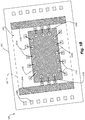
- Figure 1B is a top plan view of the assembly 100 with the casing 115 and the memory dies 106 shown in Figure 1A removed for purposes of illustration.
- the controller die 103 is located within a perimeter, or footprint 107 (shown in hidden lines), of the stack of memory dies 106 ( Figure 1A ) superimposed on the package substrate 102.
- the first and second support members 130a and 130b are also positioned within the footprint 107 and extend along first and second sides 105a and 105b, respectively, of the controller die 103.
- the support members 130 can each include an elongate member formed from an interposer substrate, a printed circuit board, a semiconductor wafer or die, or another suitable support material.
- the support members 130 can be pieces of semiconductor material that are cleaved (e.g., diced or singulated) from a semiconductor wafer or die, such as a "blank" silicon wafer or die.
- Figure 2 is a top plan view of a semiconductor wafer 220 that has been cleaved to form the support members 130 with die attach materials 141 in accordance with an embodiment of the present technology.
- the support members 130 are formed by first covering the semiconductor wafer 220 with a die-attach material 240 (e.g., a die-attach film) and then simultaneously cutting the wafer 220 and the die-attach material 240 along multiple dicing lines 221. Once cut, the support members 130 can then be attached to the package substrate 102 ( Figure 1A ) via the die-attach materials 141 formed from the respective portions of die-attach material 240.
- the support members 130 can be formed from a blank silicon wafer.
- support members can be formed from portions of a semiconductor wafer that might otherwise be discarded.
- support members 230 can be formed from an edge portion 223 of the semiconductor wafer 220 left over after die singulation.
- non-yielding or non-functioning dies can also be cut into multiple pieces to form individual spacer members.
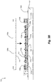
- Figures 3A-3C are cross-sectional views illustrating the assembly 100 at various stages of manufacture in accordance with an embodiment of the present technology.
- the controller die 103 is attached to the package substrate 102 with the die-attach material 140, and the first and second support members 130a-b are attached to the package substrate with die-attach materials 141a-b, respectively.
- one or more of the die-attach materials 140 and 141a-b can include a pressure-set film that adheres materials together when it is compressed (e.g., between the package substrate 102 and each of the support members 130) beyond a threshold level of pressure.
- one or more of the die-attach materials 140 and 141a-b can be a UV-set film that is set by exposure to UV radiation.
- Figure 3B shows the assembly 100 after forming the first wirebonds 111a between the first bond pads 108a of the package substrate 102 and the corresponding bond pads 109a of the controller die 103.
- the support members 130 can have a first thickness ti that is greater than a second thickness t 2 of the controller die 103.
- the first and second thicknesses t 1 and t 2 can be selected such that a wire portion 312 of each of the first wirebonds 111a does not contact the die-attach material 142 when the first memory die 106a is mounted to the support members 130.
- the thicknesses t 1 and t 2 can be selected such that the wire portion 312 projects at least partially into the die-attach material 142. In either case, once the first wirebonds 111a are formed, the first memory die 106a can be attached to the support members 130 via the die-attach material 142.
- Figure 3C shows the assembly 100 after forming the second wirebonds 111b between the second bond pads 108b of the package substrate 102 and the corresponding bond pads 109b of the first memory die 106a.
- the second memory die 106b can be attached to the first memory die 106a with the over-wire material 143.
- processing can continue with subsequent manufacturing stages. For example, processing can continue by wire bonding the second memory die 106b to the package substrate 102 and then molding the package casing 115 ( Figure 1A ) over the die stack.
- one or more additional memory dies 306 (shown in hidden lines) can be stacked above the second memory die 106b and wirebonded to the second bond pads 108b of the package substrate 102.
- Figure 4 is a cross-sectional view of a semiconductor die assembly 400 (“assembly 400") configured in accordance with another embodiment of the present technology.
- the assembly 400 can include features generally similar to those of the assembly 100 described in detail above.
- the assembly 400 includes the controller die 103 and the support members 130 attached to the package substrate 120 by the die-attach materials 140 and 141a-b.
- individual memory dies 406 are staggered such that individual bond pads 409 of the memory dies 406 are exposed along at least one edge of the stack of memory dies 406.
- wirebonds 411 can be bonded to the exposed bond pads 409 such that they are not covered by a film-over-wire material (e.g., the over-wire material 143 of Figure 1A ).
- the memory dies 406 can be assembled using a relatively thinner die-attach material 440 than a film-over-wire material.
- the stack of memory dies 406 can have a smaller height than a stack of the same number of memory dies attached together with the thicker film-over-wire material.
- FIG. 5 is a top plan view of a semiconductor die assembly 500 (“assembly 500") configured in accordance with another embodiment of the present technology.
- the assembly 500 can include features generally similar to those of the assemblies described in detail above.
- the assembly 500 includes the controller die 103 positioned within the footprint 107 of the memory dies 106 ( Figure 1A ).
- the assembly 500 can also include capacitors 550 also within the footprint 107 and coupled to the package substrate 102 via bond pads 508.
- the capacitors 550 can include, for example, monolithic (e.g., ceramic), integrated circuit, or other suitable capacitor devices.
- the capacitors 550 can be configured to condition power signals or facilitate power-up.
- the assembly 500 can include additional or alternate circuit elements (e.g., inductors, resistors, and/or diodes) and/or circuit components, such as another semiconductor dies at least partially within the footprint 107.
- Figures 6A and 6B are top plan views illustrating semiconductor die assemblies 600a and 600b, respectively, configured in accordance with several embodiments of the present technology.
- the assemblies 600a and 600b can each include features generally similar to those of the assemblies described in detail above.
- the semiconductor die assemblies 600a and 600b can each include the cavity 118 between the package substrate 102 and the memory dies 106 ( Figure 1A ) formed by the support members 130.
- the semiconductor die assembly 600a includes a third support member 630 (e.g., an elongate member) extending in a direction generally transverse to each of the support members 130.
- the third support member 630 can be spaced apart from the support members 130 by gaps Gi on opposite sides of the third support member 630 to facilitate flow of the encapsulant 116 into the cavity 118 to form the casing 115 ( Figure 1A ).
- the semiconductor die assembly 600b can include support members 635 positioned at each side the controller die 103. Similar to the third support member 630 shown in Figure 6A , the support members 635 can be separated from the support members by gaps G 2 to facilitate flow of the encapsulant 116 into the cavity 118.
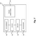
- the system 790 can include a semiconductor die assembly 700, a power source 792, a driver 794, a processor 796, and/or other subsystems or components 798.
- the semiconductor die assembly 700 can include features generally similar to those of the stacked semiconductor die assemblies described above.
- the resulting system 790 can perform any of a wide variety of functions, such as memory storage, data processing, and/or other suitable functions.
- representative systems 790 can include, without limitation, hand-held devices (e.g., mobile phones, tablets, digital readers, and digital audio players), computers, and appliances.
- Components of the system 790 may be housed in a single unit or distributed over multiple, interconnected units (e.g., through a communications network).
- the components of the system 790 can also include remote devices and any of a wide variety of computer readable media.
Landscapes
- Semiconductor Memories (AREA)
- Engineering & Computer Science (AREA)
- Manufacturing & Machinery (AREA)
Abstract
Description
- The disclosed embodiments relate to semiconductor die assemblies and to support members in such assemblies. In several embodiments, the present technology relates to die assemblies that can include a controller die and memory dies carried above the controller die.
- Packaged semiconductor dies, including memory chips, microprocessor chips, and imager chips, can include semiconductor dies mounted on a package substrate. The semiconductor dies are encased in a plastic protective covering, and each die includes functional features, such as memory cells, processor circuits, and imager devices. Bond pads on the dies are electrically connected between the functional features and terminals on the package substrate that allow the dies to be connected to external circuitry.
- To increase the density of dies within a package, the dies can be stacked upon one another within the casing. One challenge with vertically stacked dies, however, is that the dies can have different sizes or footprints. For example, in a memory package, a memory controller die can have a smaller footprint than the memory dies within the package. The memory controller die can be more difficult to wirebond because it is offset from the memory dies. Also, the memory dies can sometimes tilt when stacked upon the smaller memory controller die.
-
-
Figure 1A is a cross-sectional view of a semiconductor die assembly configured in accordance with an embodiment of the present technology, andFigure 1B is a top plan view of the assembly ofFigure 1A with a casing and a semiconductor die stack removed from the assembly. -
Figure 2 is a top plan view of a semiconductor wafer that has been cleaved to form support members of the semiconductor die assembly in accordance with an embodiment of the present technology. -
Figures 3A-3C are cross-sectional views illustrating the semiconductor die assembly ofFigure 1A at various stages of manufacture in accordance with an embodiment of the present technology. -
Figure 4 is a cross-sectional view of a semiconductor die assembly configured in accordance with another embodiment of the present technology. -
Figure 5 is a top plan view of a semiconductor die assembly configured in accordance with another embodiment of the present technology. -
Figures 6A and 6B are top plan views illustrating semiconductor die assemblies configured in accordance with several embodiments of the present technology. -
Figure 7 is a schematic view of a system that includes a semiconductor die assembly configured in accordance with embodiments of the present technology. - Specific details of several embodiments of stacked semiconductor die assemblies having spacer support members and associated systems and methods are described below. The term "semiconductor die" generally refers to a die having integrated circuits or components, data storage elements, processing components, and/or other features manufactured on semiconductor substrates. For example, semiconductor dies can include integrated circuit memory and/or logic circuitry. Semiconductor dies and/or other features in semiconductor die packages can be said to be in "thermal contact" with one another if the two structures can exchange energy through heat. A person skilled in the relevant art will also understand that the technology may have additional embodiments, and that the technology may be practiced without several of the details of the embodiments described below with reference to
Figures 1-7 . - As used herein, the terms "vertical," "lateral," "upper" and "lower" can refer to relative directions or positions of features in the semiconductor die assemblies in view of the orientation shown in the Figures. For example, "upper" or "uppermost" can refer to a feature positioned closer to the top of a page than another feature. These terms, however, should be construed broadly to include semiconductor devices having other orientations, such as being flipped on their side or inverted.
-
Figure 1A is a cross-sectional view of a semiconductor die assembly 100 ("assembly 100") configured in accordance with an embodiment of the present technology. As shown, theassembly 100 includes apackage substrate 102 carrying a first semiconductor die, or controller die 103, and first andsecond support members members 130") on opposite sides of the controller die 103. Thesupport members 130 carry first and second semiconductor dies, or first and second memory dies 106a and 106b (collectively "memory dies 106"), arranged in a stack above the controller die 103. Thepackage substrate 102 includes a plurality offirst bond pads 108a within the footprint (e.g., directly beneath) the first memory die 106a and a plurality ofsecond bond pads 108b outside of the footprint (e.g., not directly beneath) the first memory die 106a. Thefirst bond pads 108a are coupled tocorresponding bond pads 109a on thecontroller die 103 byfirst wire bonds 111a, and thesecond bond pads 108b are coupled tocorresponding bond pads 109b on each of the memory dies 106 bysecond wire bonds 111b. Thepackage substrate 102 can include, for example, a printed circuit board or other suitable substrate having electrical connectors 104 (shown schematically), such as metal traces, vias, or other suitable connectors. Theelectrical connectors 104 can couple thefirst bond pads 108a and/or thesecond bond pads 108b to external circuitry (not shown) viapackage contacts 113 and interconnects 114 (e.g., bump bonds) at the opposite side of thepackage substrate 102. In several embodiments, theelectrical connectors 104 can also couple individualfirst bond pads 108a with individualsecond bond pads 108b to electrically intercouple the controller die 103 with the memory dies 106. - The
assembly 100 further includes apackage casing 115 composed of anencapsulant 116 that at least partially encapsulates the controller die 103, the memory dies 106, and thesupport members 130. In the illustrated embodiment, theencapsulant 116 also extends into acavity 118 between thepackage substrate 102 and the first memory die 106a to at least partially fill the region beneath thefirst memory die 106a not occupied by the controller die 103 and the support members. In some embodiments, the portion of theencapsulant 116 in thecavity 118 can reinforce thesupport members 130 and provide further mechanical support beneath thefirst memory die 106a. The encapsulant 116 can include, for example, a thermoset material, an epoxy resin, or other suitable compound that provides mechanical support, shielding from the ambient environment (e.g., from humidity), and/or electrical isolation (e.g., between wire bonds). - The controller die 103 and the memory dies 106 can each be formed from a semiconductor substrate, such as silicon, silicon-on-insulator, compound semiconductor (e.g., Gallium Nitride), or other suitable substrate. The semiconductor substrate can be cut or singulated into semiconductor dies having any of variety of integrate circuit components or functional features, such as dynamic random-access memory (DRAM), static random-access memory (SRAM), flash memory, other forms of integrated circuit devices, including memory, processing circuits, imaging components, and/or other semiconductor devices. In selected embodiments, the
assembly 100 can be configured as a memory in which the memory dies 106 provide data storage (e.g., NAND dies) and the controller die 103 provides memory control (e.g., NAND control). In some embodiments, theassembly 100 can include other semiconductor dies in addition to and/or in lieu of one or more of the controller die 103 and/or the memory dies 106. For example, instead of two memory dies, theassembly 100 can include more than two memory dies (e.g., four dies, eight dies, etc.) or only a single memory die. Further, in various embodiments, the dies of theassembly 100 can have different sizes. For example, in some embodiments one or both of the memory dies 106 can extend beyond thesupport members 130 at one or more sides. - As further shown in
Figure 1A , the controller die 103 is attached to thepackage substrate 102 by a die-attach material 140 (e.g., a die-attach film). Thefirst support member 130a is attached to thepackage substrate 102 by a die-attach material 141a, and thesecond support member 130b is attached to thepackage substrate 102 by a die-attach material 141b. The memory dies 106, in turn, are attached to the controller die 103 and thesupport members 130 by a die-attach material 142 and to one another by a film-over-wire material 143 ("over-wirematerial 142"). In several embodiments, the die-attach materials material 143 can be formed from the same orsimilar materials material 143 can have a greater thickness to accommodate awire portion 112 of thefirst wire bonds 111a between the memory dies 106. In selected embodiments, the die-attach materials material 143 can each include a laminate film of epoxy-based material. Such laminate films can include, for example, a die-attach film or a dicing-die-attach film (known to those skilled in the art as "DAFs" or "DDFs," respectively). In one embodiment the die-attach materials and/or film-over wire materials can each include DAFs or DDFs provided by Henkel AG & Co. of Shangai, China (e.g., Model Nos. Ablestick ATB-100, 100U, 100A, 100U). - In some conventional package assemblies, the controller die can be positioned between the package substrate and a stack of memory dies. This configuration is typically formed by encapsulating the controller die with an encapsulant and then the memory dies are stacked upon the surface of the encapsulant. One challenge with encapsulating the controller die at this stage, however, is that it complicates manufacturing. For example, the mounting surface on the encapsulant can be uneven. When the memory dies are stacked on an uneven mounting surface, they can cant or tilt to the extent that the dies project outside of the protective casing. Also, die tilt can make wirebonding more difficult because the wire bonds have different lengths at the opposite sides of the assembly. Another conventional manufacturing technique involves forming a cavity in the package substrate into which the controller die can be inserted. This technique can also complicate manufacturing and increase costs because it requires the package substrate to be milled or etched to form the cavity.
- Embodiments of die assemblies configured in accordance with several embodiments of the present technology can address these and other limitations of conventional die assemblies. For example, one advantage is that the stack of memory dies 106 can be mounted to the
support members 130 without having to first encapsulate the controller die 103 beneath the memory dies 106. A related advantage is that the high temperature molding and curing steps for encapsulating the controller die can be eliminated and thus reduce thermal cycling. Accordingly, manufacturing can be less complicated because it can eliminate several manufacturing steps. Another advantage is that thesupport members 130 can have a coefficient of thermal expansion (CTE) that is similar to or the same as the memory dies 106. For example, thesupport members 130 can be formed from semiconductor materials, such as silicon. Such CTE matching reduces thermal stresses within the package during operation. Yet another advantage is that the memory dies 106 are not prone to tilt because thesupport members 130 can have the same height and the die-attachmaterials -
Figure 1B is a top plan view of theassembly 100 with thecasing 115 and the memory dies 106 shown inFigure 1A removed for purposes of illustration. As shown, the controller die 103 is located within a perimeter, or footprint 107 (shown in hidden lines), of the stack of memory dies 106 (Figure 1A ) superimposed on thepackage substrate 102. The first andsecond support members footprint 107 and extend along first andsecond sides support members 130 can each include an elongate member formed from an interposer substrate, a printed circuit board, a semiconductor wafer or die, or another suitable support material. In one embodiment described in greater detail below, thesupport members 130 can be pieces of semiconductor material that are cleaved (e.g., diced or singulated) from a semiconductor wafer or die, such as a "blank" silicon wafer or die. -
Figure 2 is a top plan view of asemiconductor wafer 220 that has been cleaved to form thesupport members 130 with die attachmaterials 141 in accordance with an embodiment of the present technology. In the illustrated embodiment, thesupport members 130 are formed by first covering thesemiconductor wafer 220 with a die-attach material 240 (e.g., a die-attach film) and then simultaneously cutting thewafer 220 and the die-attachmaterial 240 along multiple dicinglines 221. Once cut, thesupport members 130 can then be attached to the package substrate 102 (Figure 1A ) via the die-attachmaterials 141 formed from the respective portions of die-attachmaterial 240. In one embodiment, thesupport members 130 can be formed from a blank silicon wafer. In another embodiment, support members can be formed from portions of a semiconductor wafer that might otherwise be discarded. For example,support members 230 can be formed from anedge portion 223 of thesemiconductor wafer 220 left over after die singulation. In additional or alternate embodiments, non-yielding or non-functioning dies can also be cut into multiple pieces to form individual spacer members. -
Figures 3A-3C are cross-sectional views illustrating theassembly 100 at various stages of manufacture in accordance with an embodiment of the present technology. Referring first toFigure 3A , the controller die 103 is attached to thepackage substrate 102 with the die-attachmaterial 140, and the first andsecond support members 130a-b are attached to the package substrate with die-attachmaterials 141a-b, respectively. In one embodiment, one or more of the die-attachmaterials package substrate 102 and each of the support members 130) beyond a threshold level of pressure. In another embodiment, one or more of the die-attachmaterials -
Figure 3B shows theassembly 100 after forming the first wirebonds 111a between thefirst bond pads 108a of thepackage substrate 102 and thecorresponding bond pads 109a of the controller die 103. As shown, thesupport members 130 can have a first thickness ti that is greater than a second thickness t2 of the controller die 103. In several embodiments, the first and second thicknesses t1 and t2 can be selected such that awire portion 312 of each of the first wirebonds 111a does not contact the die-attachmaterial 142 when thefirst memory die 106a is mounted to thesupport members 130. In another embodiment, the thicknesses t1 and t2 can be selected such that thewire portion 312 projects at least partially into the die-attachmaterial 142. In either case, once the first wirebonds 111a are formed, thefirst memory die 106a can be attached to thesupport members 130 via the die-attachmaterial 142. -
Figure 3C shows theassembly 100 after forming thesecond wirebonds 111b between thesecond bond pads 108b of thepackage substrate 102 and thecorresponding bond pads 109b of thefirst memory die 106a. After thesecond wirebonds 111b are formed, thesecond memory die 106b can be attached to thefirst memory die 106a with theover-wire material 143. Once the memory dies 106 are attached to one another, processing can continue with subsequent manufacturing stages. For example, processing can continue by wire bonding thesecond memory die 106b to thepackage substrate 102 and then molding the package casing 115 (Figure 1A ) over the die stack. In some embodiments, one or more additional memory dies 306 (shown in hidden lines) can be stacked above thesecond memory die 106b and wirebonded to thesecond bond pads 108b of thepackage substrate 102. -
Figure 4 is a cross-sectional view of a semiconductor die assembly 400 ("assembly 400") configured in accordance with another embodiment of the present technology. Theassembly 400 can include features generally similar to those of theassembly 100 described in detail above. For example, theassembly 400 includes the controller die 103 and thesupport members 130 attached to the package substrate 120 by the die-attachmaterials Figure 4 , individual memory dies 406 are staggered such thatindividual bond pads 409 of the memory dies 406 are exposed along at least one edge of the stack of memory dies 406. In one aspect of this embodiment, wirebonds 411 can be bonded to the exposedbond pads 409 such that they are not covered by a film-over-wire material (e.g., theover-wire material 143 ofFigure 1A ). As such, the memory dies 406 can be assembled using a relatively thinner die-attachmaterial 440 than a film-over-wire material. Also, the stack of memory dies 406 can have a smaller height than a stack of the same number of memory dies attached together with the thicker film-over-wire material. -
Figure 5 is a top plan view of a semiconductor die assembly 500 ("assembly 500") configured in accordance with another embodiment of the present technology. Theassembly 500 can include features generally similar to those of the assemblies described in detail above. For example, theassembly 500 includes the controller die 103 positioned within thefootprint 107 of the memory dies 106 (Figure 1A ). In the illustrated embodiment ofFigure 5 , theassembly 500 can also includecapacitors 550 also within thefootprint 107 and coupled to thepackage substrate 102 viabond pads 508. Thecapacitors 550 can include, for example, monolithic (e.g., ceramic), integrated circuit, or other suitable capacitor devices. In several embodiments, thecapacitors 550 can be configured to condition power signals or facilitate power-up. In other embodiments, theassembly 500 can include additional or alternate circuit elements (e.g., inductors, resistors, and/or diodes) and/or circuit components, such as another semiconductor dies at least partially within thefootprint 107. -
Figures 6A and 6B are top plan views illustrating semiconductor dieassemblies assemblies assemblies cavity 118 between thepackage substrate 102 and the memory dies 106 (Figure 1A ) formed by thesupport members 130. - Referring to
Figure 6A , thesemiconductor die assembly 600a includes a third support member 630 (e.g., an elongate member) extending in a direction generally transverse to each of thesupport members 130. In one aspect of this embodiment, thethird support member 630 can be spaced apart from thesupport members 130 by gaps Gi on opposite sides of thethird support member 630 to facilitate flow of theencapsulant 116 into thecavity 118 to form the casing 115 (Figure 1A ). Referring toFigure 6B , thesemiconductor die assembly 600b can includesupport members 635 positioned at each side the controller die 103. Similar to thethird support member 630 shown inFigure 6A , thesupport members 635 can be separated from the support members by gaps G2 to facilitate flow of theencapsulant 116 into thecavity 118. - Any one of the stacked semiconductor die assemblies described above with reference to
Figures 1-6B can be incorporated into any of a myriad of larger and/or more complex systems, a representative example of which issystem 790 shown schematically inFigure 7 . Thesystem 790 can include asemiconductor die assembly 700, apower source 792, adriver 794, aprocessor 796, and/or other subsystems orcomponents 798. The semiconductor dieassembly 700 can include features generally similar to those of the stacked semiconductor die assemblies described above. The resultingsystem 790 can perform any of a wide variety of functions, such as memory storage, data processing, and/or other suitable functions. Accordingly,representative systems 790 can include, without limitation, hand-held devices (e.g., mobile phones, tablets, digital readers, and digital audio players), computers, and appliances. Components of thesystem 790 may be housed in a single unit or distributed over multiple, interconnected units (e.g., through a communications network). The components of thesystem 790 can also include remote devices and any of a wide variety of computer readable media. - From the foregoing, it will be appreciated that specific embodiments of the technology have been described herein for purposes of illustration, but that various modifications may be made without deviating from the disclosure. Also, certain aspects of the new technology described in the context of particular embodiments may also be combined or eliminated in other embodiments. Moreover, although advantages associated with certain embodiments of the new technology have been described in the context of those embodiments, other embodiments may also exhibit such advantages and not all embodiments need necessarily exhibit such advantages to fall within the scope of the technology. Accordingly, the disclosure and associated technology can encompass other embodiments not expressly shown or described herein.
- The following are numbered examples that form part of this disclosure:
- 1. A semiconductor die assembly, comprising:
- a package substrate;
- a first semiconductor die attached to the package substrate;
- a plurality of support members attached to the package substrate, the plurality of support members including a first support member and a second support member disposed on opposite sides of the first semiconductor die; and
- a second semiconductor die coupled to the plurality of support members such that at least a portion of the second semiconductor die is over the first semiconductor die.
- 2. The semiconductor die assembly of example 1 wherein the package substrate further includes:
- a plurality of first bond pads electrically coupled to the first semiconductor die, wherein at least a portion of the first bond pads are directly beneath the second semiconductor die; and
- a plurality of second bond pads electrically coupled to the second semiconductor die, wherein the second bond pads extend outside of the second semiconductor die.
- 3. The semiconductor die assembly of example 2, further comprising:
- a plurality of first wirebonds electrically coupling the first bond pads to corresponding bond pads of the first semiconductor die; and
- a plurality of second wirebonds electrically coupling the second bond pads to corresponding bond pads of the second semiconductor die.
- 4. The semiconductor die assembly of example 1 wherein the plurality of support members, the second semiconductor die, and the package substrate together define a cavity beneath the second semiconductor die, and wherein the semiconductor die assembly further comprises a package casing that includes an encapsulant at least partially extending into the cavity.
- 5. The semiconductor die assembly of example 1, further comprising a die-attach film attaching the first semiconductor die to the package substrate.
- 6. The semiconductor die assembly of example 5, further comprising separate die-attach films attaching each of the support members to the package substrate.
- 7. The semiconductor die assembly of example 1, further comprising a die-attach film attaching each of the support members to the second semiconductor die, but not attaching the first semiconductor die to the second semiconductor die.
- 8. A semiconductor die assembly, comprising:
- a package substrate;
- a memory die;
- a plurality of support members attached to the package substrate and the memory dies, wherein the memory die is spaced apart from the package substrate; and
- a controller die on the package substrate, wherein the controller die is between the package substrate and the memory die.
- 9. The semiconductor die assembly of example 8, further comprising a die-attach film attaching each of the support members to the memory die.
- 10. The semiconductor die assembly of example 9 wherein the controller die is spaced apart from the die-attach film.
- 11. The semiconductor die assembly of example 8 wherein the plurality of support members includes first and second elongate members at opposite sides of the controller die and in parallel with one another.
- 12. The semiconductor die assembly of example 11 wherein the first and second elongate members each include silicon.
- 13. The semiconductor die assembly of example 11, further comprising a third elongate member extending laterally between first and second elongate members.
- 14. The semiconductor die assembly of example 8, further comprising:
- a first die-attach material attaching the controller die to the package substrate;
- a second die-attach material attaching the first elongate member to the package substrate;
- a third die-attach material attaching the second elongate member to the package substrate; and
- a fourth die-attach material attaching both the first and second elongate members to the memory die.
- 15. The semiconductor die assembly of example 14 wherein the first, second, third, and fourth die-attach materials each include a die-attach film.
- 16. The semiconductor die assembly of example 8 wherein the memory die is a first memory die, and wherein the semiconductor die assembly further includes a second memory die stacked upon the first memory die.
- 17. The semiconductor die assembly of example 16 wherein:
- the first memory die includes a plurality of bond pads; and
- the second memory die is staggered relative to the first memory die such that the bond pads are exposed on at least one side of the first memory die.
- 18. The semiconductor die assembly of example 8, further comprising a circuit component positioned below the memory die and at least partially within the footprint of the memory die, wherein the circuit component is separated from the controller die on the package substrate.
- 19. The semiconductor die assembly of example 18 wherein the circuit component is a capacitor.
- 20. A method of manufacturing a semiconductor die assembly, the method comprising:
- attaching a first semiconductor die to a package substrate;
- positioning a first support member and a second support member on different sides of the first semiconductor die; and
- attaching a second semiconductor die to the first and second support members such that the first and second support members carry the second semiconductor die above the first semiconductor die.
- 21. The method of example 20, further comprising:
- wirebonding first bond pads of the package substrate to corresponding bond pads of the first semiconductor die; and
- wirebonding second bond pads of the package substrate to corresponding bond pads of the second semiconductor die,
- wherein the first bond pads are within a footprint of the first semiconductor die.
- 22. The method of example 20 wherein the first and second support members, the second semiconductor die, and the package substrate together define a cavity beneath the second semiconductor die, and wherein the method further includes flowing an encapsulant into the cavity.
- 23. The method of example 20 wherein attaching the first semiconductor die to the package substrate includes attaching the first semiconductor die to the package substrate with a die-attach film.
- 24. The method of example 20 wherein forming the first support member and the second support member includes:
- attaching the first support member to the package substrate with a first die-attach film; and
- attaching the second support members to the package substrate with a second die-attach film.
- 25. The method of example 20 wherein attaching the second semiconductor die to the first and second support members includes attaching a die-attach film to each of the second semiconductor die and the first and second support members, but not attaching the die-attach film to the first semiconductor die.
- 26. The method of example 25, further comprising forming wirebonds that electrically couple the first semiconductor die with the package substrate, wherein a portion of the wirebonds project into the die-attach film.
- 27. The method of example 20 wherein forming the first support member and the second support member includes:
- covering a semiconductor wafer with a die-attach material;
- cutting the semiconductor wafer to form elongate semiconductor members each having a portion of the die-attach material attached thereto; and
- attaching the elongate semiconductor members to the package substrate via the portion of the die-attach material attached to each of the elongate semiconductor members.
- 28. A method of manufacturing a semiconductor die assembly, the method comprising:
- attaching a plurality of support members to a package substrate;
- attaching a controller die to a portion of the package substrate, wherein the portion of the package substrate is within a perimeter defined by the plurality of support members on the substrate; and
- mounting a memory die to the plurality of support members.
- 29. The method of example 28 wherein:
- attaching the plurality of support members to the package substrate includes attaching a first support member to the package substrate with a first die-attach material and attaching a second support member to the package substrate with a second die-attach material;
- attaching the controller die to the portion of the package substrate includes attaching the controller die to the portion of the package substrate with a third die-attach material; and
- mounting the memory die to the plurality of support members includes attaching the memory die to both of the first and second support members with a fourth die-attach material.
- 30. The method of example 29 wherein the first, second, third, and fourth die-attach materials each include a die-attach film.
- 31. The method of example 29 wherein the first, second, third, and fourth die-attach materials each include a pressure-set die-attach film.
- 32. The method of example 28, further comprising forming wirebonds beneath the memory die to electrically couple the controller die to the package substrate.
- 33. The method of example 32 wherein mounting the memory die to the plurality of support members includes forming a die-attach film that contacts the wirebonds but not the controller die.
- 34. The method of example 28 wherein the memory die is a first memory die, and wherein the method further comprises stacking a second memory die on top of the first memory die.
- 35. The method of example 34 wherein stacking the second memory die on top of the first memory die includes stacking the second memory die such that the second memory die is staggered relative to the first memory die.
- 36. The method of example 28, further comprising attaching a circuit component to a portion of the package substrate at least partially within the perimeter defined by the plurality of support members on the substrate.
- 37. The method of example 28 wherein the circuit component includes a capacitor.
Claims (15)
- A method of manufacturing a semiconductor die assembly, the method comprising:attaching a controller die to a package substrate;attaching a first support member and a second support member to the package substrate on different sides of the controller die; andattaching a first memory die to the first and second support members such that the first and second support members carry the first memory die above the controller die.
- The method of claim 1 wherein attaching the first support member and the second support member includes:covering a semiconductor wafer with a die-attach material;cutting the semiconductor wafer to form elongate semiconductor members each having a portion of the die-attach material attached thereto, wherein the elongate semiconductor members include the first and second support members; andattaching the first and second support members to the package substrate via the portions of the die-attach material.
- The method of any preceding claim wherein:attaching the first support member and the second support member to the package substrate includes attaching the first support member to the package substrate with a first die-attach material and attaching the second support member to the package substrate with a second die-attach material;attaching the controller die to the package substrate includes attaching the controller die to a portion of the package substrate with a third die-attach material, wherein the portion of the package substrate is within a perimeter defined by the first and second support members on the substrate; andattaching the first memory die to the first and second support members includes attaching the first memory die to both of the first and second support members with a fourth die-attach material.
- The method of claim 3 wherein the first, second, third, and fourth die-attach materials each include a pressure-set die-attach film or a UV-set die-attach film.
- The method of any preceding claim further comprising stacking a second memory die on top of the first memory die, wherein stacking the second memory die on top of the first memory die comprises attaching the second memory die to the first memory die by a film-over-wire material.
- The method of claim 5 when dependent on claim 3 wherein the film-over-wire material is formed from the same or similar material to the first, second, third, and fourth die-attach materials, and wherein the film-over-wire material has a greater thickness than the first, second, third, and fourth die-attach materials to thereby accommodate a wire portion of first wire bonds between the first memory die and the second memory die.
- The method of any preceding claim wherein attaching the first memory die to the first and second support members includes attaching a die-attach material to each of the first memory die and the first and second support members, but not attaching the die-attach material to the controller die.
- The method of claim 7, further comprising forming wirebonds that electrically couple the controller die with the package substrate, wherein a portion of the wirebonds project into the die-attach material.
- The method of any preceding claim wherein the first and second support members, the first memory die, and the package substrate together define a cavity beneath the first memory die, and wherein the method further includes flowing an encapsulant into the cavity.
- The method of any preceding claim further comprising stacking a second memory die on top of the first memory die, wherein stacking the second memory die on top of the first memory die includes stacking the second memory die such that the second memory die is staggered relative to the first memory die.
- A semiconductor die assembly, comprising:a package substrate;a controller die attached to the package substrate;a plurality of support members attached to the package substrate, the plurality of support members including a first support member and a second support member disposed on opposite sides of the controller die; anda first memory die coupled to the plurality of support members such that at least a portion of the first memory die is over the controller die.
- The semiconductor die assembly of claim 11, further comprising: a first die attach material attaching the first support member to the package substrate and a second die-attach material attaching the second support member to the package substrate, and a third die-attach material attaching the controller die to the package substrate, and further comprising a fourth die-attach material attaching each of the support members to the first memory die, but not attaching the controller die to the first memory die.
- The semiconductor die assembly of claim 11 or claim 12 wherein the first and second support members each include silicon.
- The semiconductor die assembly of any of claims 11-13 wherein the semiconductor die assembly further includes a second memory die stacked upon the first memory die, wherein the second memory die is attached to the first memory die by a film-over-wire material.
- The semiconductor die assembly of claim 14 when dependent on claim 12 wherein the film-over-wire material is formed from the same or similar material to the first, second, third, and fourth die-attach materials, and wherein the film-over-wire material has a greater thickness than the first, second, third, and fourth die-attach materials to thereby accommodate a wire portion of first wire bonds between the first memory die and the second memory die.
Applications Claiming Priority (3)
| Application Number | Priority Date | Filing Date | Title |
|---|---|---|---|
| US14/264,584 US9418974B2 (en) | 2014-04-29 | 2014-04-29 | Stacked semiconductor die assemblies with support members and associated systems and methods |
| EP15785531.3A EP3138124A4 (en) | 2014-04-29 | 2015-04-29 | Stacked semiconductor die assemblies with support members and associated systems and methods |
| PCT/US2015/028138 WO2015168206A1 (en) | 2014-04-29 | 2015-04-29 | Stacked semiconductor die assemblies with support members and associated systems and methods |
Related Parent Applications (1)
| Application Number | Title | Priority Date | Filing Date |
|---|---|---|---|
| EP15785531.3A Division EP3138124A4 (en) | 2014-04-29 | 2015-04-29 | Stacked semiconductor die assemblies with support members and associated systems and methods |
Publications (1)
| Publication Number | Publication Date |
|---|---|
| EP3869556A1 true EP3869556A1 (en) | 2021-08-25 |
Family
ID=54335491
Family Applications (2)
| Application Number | Title | Priority Date | Filing Date |
|---|---|---|---|
| EP15785531.3A Ceased EP3138124A4 (en) | 2014-04-29 | 2015-04-29 | Stacked semiconductor die assemblies with support members and associated systems and methods |
| EP20216842.3A Pending EP3869556A1 (en) | 2014-04-29 | 2015-04-29 | Stacked semiconductor die assemblies with support members and associated systems and methods |
Family Applications Before (1)
| Application Number | Title | Priority Date | Filing Date |
|---|---|---|---|
| EP15785531.3A Ceased EP3138124A4 (en) | 2014-04-29 | 2015-04-29 | Stacked semiconductor die assemblies with support members and associated systems and methods |
Country Status (8)
| Country | Link |
|---|---|
| US (5) | US9418974B2 (en) |
| EP (2) | EP3138124A4 (en) |
| JP (1) | JP6422508B2 (en) |
| KR (1) | KR101910263B1 (en) |
| CN (2) | CN113257803A (en) |
| SG (2) | SG11201608741TA (en) |
| TW (1) | TWI634628B (en) |
| WO (1) | WO2015168206A1 (en) |
Families Citing this family (45)
| Publication number | Priority date | Publication date | Assignee | Title |
|---|---|---|---|---|
| KR20150039284A (en) * | 2013-10-02 | 2015-04-10 | 삼성전자주식회사 | Multi-chip package |
| US9418974B2 (en) | 2014-04-29 | 2016-08-16 | Micron Technology, Inc. | Stacked semiconductor die assemblies with support members and associated systems and methods |
| US9627367B2 (en) * | 2014-11-21 | 2017-04-18 | Micron Technology, Inc. | Memory devices with controllers under memory packages and associated systems and methods |
| KR20170053416A (en) * | 2015-11-06 | 2017-05-16 | 주식회사 엘지화학 | Semiconductor device and manufacturing method of the same |
| US9875993B2 (en) * | 2016-01-14 | 2018-01-23 | Micron Technology, Inc. | Semiconductor devices with duplicated die bond pads and associated device packages and methods of manufacture |
| WO2018058416A1 (en) | 2016-09-29 | 2018-04-05 | Intel Corporation | Prepackaged stair-stacked memory module in a chip scale system in package, and methods of making same |
| US20190229093A1 (en) * | 2016-10-01 | 2019-07-25 | Intel Corporation | Electronic device package |
| US10147705B2 (en) | 2017-02-21 | 2018-12-04 | Micron Technology, Inc. | Stacked semiconductor die assemblies with die substrate extensions |
| WO2018182752A1 (en) * | 2017-04-01 | 2018-10-04 | Intel Corporation | Electronic device package |
| US20190013214A1 (en) * | 2017-07-10 | 2019-01-10 | Powertech Technology Inc. | Package structure and manufacturing method thereof |
| US10217726B1 (en) * | 2017-08-31 | 2019-02-26 | Micron Technology, Inc. | Stacked semiconductor dies including inductors and associated methods |
| US10312219B2 (en) * | 2017-11-08 | 2019-06-04 | Micron Technology, Inc. | Semiconductor device assemblies including multiple shingled stacks of semiconductor dies |
| US10504854B2 (en) * | 2017-12-07 | 2019-12-10 | Intel Corporation | Through-stiffener inerconnects for package-on-package apparatus and methods of assembling same |
| US10548230B2 (en) * | 2018-01-04 | 2020-01-28 | Micron Technology, Inc. | Method for stress reduction in semiconductor package via carrier |
| KR20190121560A (en) | 2018-04-18 | 2019-10-28 | 삼성전기주식회사 | Fan-out semiconductor package |
| KR102592327B1 (en) * | 2018-10-16 | 2023-10-20 | 삼성전자주식회사 | Semiconductor package |
| WO2020100308A1 (en) * | 2018-11-16 | 2020-05-22 | 日立化成株式会社 | Semiconductor device and manufacturing method thereof, and structure used in manufacture of semiconductor device |
| US11557541B2 (en) * | 2018-12-28 | 2023-01-17 | Intel Corporation | Interconnect architecture with silicon interposer and EMIB |
| US10978426B2 (en) * | 2018-12-31 | 2021-04-13 | Micron Technology, Inc. | Semiconductor packages with pass-through clock traces and associated systems and methods |
| WO2020217394A1 (en) | 2019-04-25 | 2020-10-29 | 日立化成株式会社 | Semiconductor device having dolmen structure and method of manufacturing same and laminate film for forming support piece and method of manufacturing same |
| JP7304703B2 (en) | 2019-02-04 | 2023-07-07 | 康子 林 | rice ball maker |
| US12027496B2 (en) | 2019-02-22 | 2024-07-02 | Intel Corporation | Film in substrate for releasing z stack-up constraint |
| WO2020217401A1 (en) | 2019-04-25 | 2020-10-29 | 日立化成株式会社 | Semiconductor device having dolmen structure, method for manufacturing same, laminated film for forming support piece, and method for manufacturing same |
| SG11202110100WA (en) * | 2019-04-25 | 2021-11-29 | Showa Denko Materials Co Ltd | Method for manufacturing semiconductor device having dolmen structure, method for manufacturing support piece, and laminate film for support piece formation |
| WO2020217411A1 (en) * | 2019-04-25 | 2020-10-29 | 日立化成株式会社 | Semiconductor device having dolmen structure and method for manufacturing same, and laminated film for forming support piece and method for manufacturing same |
| JP7351335B2 (en) * | 2019-04-25 | 2023-09-27 | 株式会社レゾナック | Semiconductor device having dolmen structure, method for manufacturing the same, method for manufacturing support piece, and laminated film for forming support piece |
| WO2020217404A1 (en) * | 2019-04-25 | 2020-10-29 | 日立化成株式会社 | Semiconductor device having dolmen structure and method for manufacturing same |
| WO2020217397A1 (en) * | 2019-04-25 | 2020-10-29 | 日立化成株式会社 | Method for producing semiconductor device having dolmen structure, method for producing supporting pieces, and multilayer film |
| JP7683478B2 (en) * | 2019-04-25 | 2025-05-27 | 株式会社レゾナック | Manufacturing method of semiconductor device having dolmen structure and manufacturing method of support piece |
| US11424212B2 (en) | 2019-07-17 | 2022-08-23 | Advanced Semiconductor Engineering, Inc. | Semiconductor package structure and method for manufacturing the same |
| US11424169B2 (en) | 2019-08-08 | 2022-08-23 | Micron Technology, Inc. | Memory device including circuitry under bond pads |
| JP7452545B2 (en) | 2019-08-29 | 2024-03-19 | 株式会社レゾナック | Method for manufacturing a support piece, method for manufacturing a semiconductor device, and laminated film for forming a support piece |
| JP2021044362A (en) * | 2019-09-10 | 2021-03-18 | キオクシア株式会社 | Semiconductor device |
| CN110634850A (en) * | 2019-09-27 | 2019-12-31 | 华天科技(西安)有限公司 | A kind of SSD stack packaging structure and preparation method thereof |
| US11456289B2 (en) | 2019-12-27 | 2022-09-27 | Micron Technology, Inc. | Face-to-face semiconductor device with fan-out porch |
| US11769752B2 (en) * | 2020-07-24 | 2023-09-26 | Micron Technology, Inc. | Stacked semiconductor die assemblies with substrate heat sinks and associated systems and methods |
| US11942460B2 (en) * | 2020-12-29 | 2024-03-26 | Micron Technology, Inc. | Systems and methods for reducing the size of a semiconductor assembly |
| CN114691555A (en) * | 2020-12-30 | 2022-07-01 | 华为技术有限公司 | Storage device and computer equipment |
| US11710722B2 (en) * | 2021-04-16 | 2023-07-25 | Micron Technology, Inc. | Semiconductor assemblies with systems and methods for managing high die stack structures |
| US12022618B2 (en) * | 2021-04-22 | 2024-06-25 | Western Digital Technologies, Inc. | Printed circuit board with stacked passive components |
| US11955345B2 (en) * | 2021-05-06 | 2024-04-09 | Micron Technology, Inc. | Encapsulation warpage reduction for semiconductor die assemblies and associated methods and systems |
| WO2023136004A1 (en) | 2022-01-11 | 2023-07-20 | 株式会社レゾナック | Laminated film and support piece manufacturing method |
| JP2023102570A (en) | 2022-01-12 | 2023-07-25 | 株式会社レゾナック | LAMINATED FILM FOR FORMING INDIVIDUALIZED BODY, METHOD FOR MANUFACTURING THE SAME, AND METHOD FOR MANUFACTURING SEMICONDUCTOR DEVICE |
| US12469772B2 (en) * | 2022-05-31 | 2025-11-11 | Texas Instruments Incorporated | Die attach film die pad isolation for semiconductor devices |
| CN118280952A (en) * | 2024-05-31 | 2024-07-02 | 甬矽电子(宁波)股份有限公司 | Chip packaging structure and manufacturing method thereof |
Citations (8)
| Publication number | Priority date | Publication date | Assignee | Title |
|---|---|---|---|---|
| KR20010073344A (en) * | 2000-01-14 | 2001-08-01 | 윤종용 | Multi chip package |
| US20020096785A1 (en) * | 2001-01-24 | 2002-07-25 | Nec Corporation | Semiconductor device having stacked multi chip module structure |
| US20030038374A1 (en) * | 2001-08-27 | 2003-02-27 | Shim Jong Bo | Multi-chip package (MCP) with spacer |
| US20090051043A1 (en) * | 2007-08-21 | 2009-02-26 | Spansion Llc | Die stacking in multi-die stacks using die support mechanisms |
| KR100894173B1 (en) * | 2008-03-31 | 2009-04-22 | 주식회사 이녹스 | Adhesive film for semiconductor package |
| US20100314740A1 (en) * | 2009-06-15 | 2010-12-16 | Samsung Electronics Co., Ltd. | Semiconductor package, stack module, card, and electronic system |
| US20130049228A1 (en) * | 2011-08-31 | 2013-02-28 | Samsung Electronics Co., Ltd. | Semiconductor package having supporting plate and method of forming the same |
| JP2013131557A (en) * | 2011-12-20 | 2013-07-04 | Toshiba Corp | Semiconductor device and method of manufacturing the same |
Family Cites Families (42)
| Publication number | Priority date | Publication date | Assignee | Title |
|---|---|---|---|---|
| US6507115B2 (en) * | 2000-12-14 | 2003-01-14 | International Business Machines Corporation | Multi-chip integrated circuit module |
| US7220615B2 (en) | 2001-06-11 | 2007-05-22 | Micron Technology, Inc. | Alternative method used to package multimedia card by transfer molding |
| US6787916B2 (en) * | 2001-09-13 | 2004-09-07 | Tru-Si Technologies, Inc. | Structures having a substrate with a cavity and having an integrated circuit bonded to a contact pad located in the cavity |
| US7132311B2 (en) * | 2002-07-26 | 2006-11-07 | Intel Corporation | Encapsulation of a stack of semiconductor dice |
| TW567601B (en) * | 2002-10-18 | 2003-12-21 | Siliconware Precision Industries Co Ltd | Module device of stacked semiconductor package and method for fabricating the same |
| TWI236117B (en) * | 2003-02-26 | 2005-07-11 | Advanced Semiconductor Eng | Semiconductor package with a heat sink |
| SG143931A1 (en) * | 2003-03-04 | 2008-07-29 | Micron Technology Inc | Microelectronic component assemblies employing lead frames having reduced-thickness inner lengths |
| US20050196907A1 (en) | 2003-09-19 | 2005-09-08 | Glenn Ratificar | Underfill system for die-over-die arrangements |
| US6930378B1 (en) * | 2003-11-10 | 2005-08-16 | Amkor Technology, Inc. | Stacked semiconductor die assembly having at least one support |
| JP2005327789A (en) * | 2004-05-12 | 2005-11-24 | Sharp Corp | Dicing / die-bonding adhesive sheet and method for manufacturing semiconductor device using the same |
| TWI292617B (en) * | 2006-02-03 | 2008-01-11 | Siliconware Precision Industries Co Ltd | Stacked semiconductor structure and fabrication method thereof |
| CN101419963B (en) * | 2006-06-06 | 2011-05-25 | 南茂科技股份有限公司 | Chip-chip package and manufacturing method thereof |
| US20080054451A1 (en) * | 2006-09-06 | 2008-03-06 | Michael Bauer | Multi-chip assembly |
| TWI331390B (en) | 2007-03-09 | 2010-10-01 | Powertech Technology Inc | Multi-chip stack package efficiently using a chip attached area on a substrate and its applications |
| US7863090B2 (en) * | 2007-06-25 | 2011-01-04 | Epic Technologies, Inc. | Packaged electronic modules and fabrication methods thereof implementing a cell phone or other electronic system |
| US7705476B2 (en) | 2007-11-06 | 2010-04-27 | National Semiconductor Corporation | Integrated circuit package |
| KR101491138B1 (en) * | 2007-12-12 | 2015-02-09 | 엘지이노텍 주식회사 | Multi-layer substrate and light-emitting diode module |
| US7750459B2 (en) | 2008-02-01 | 2010-07-06 | International Business Machines Corporation | Integrated module for data processing system |
| CN101232011B (en) * | 2008-02-21 | 2010-09-08 | 日月光半导体制造股份有限公司 | Stacked chip package structure and manufacturing method thereof |
| US7956449B2 (en) * | 2008-06-25 | 2011-06-07 | Stats Chippac Ltd. | Stacked integrated circuit package system |
| US8923004B2 (en) | 2008-07-31 | 2014-12-30 | Micron Technology, Inc. | Microelectronic packages with small footprints and associated methods of manufacturing |
| CN101661927A (en) * | 2008-08-26 | 2010-03-03 | 南茂科技股份有限公司 | Chip package |
| KR20110055683A (en) * | 2008-09-22 | 2011-05-25 | 히다치 가세고교 가부시끼가이샤 | Semiconductor device and manufacturing method thereof |
| US7732252B2 (en) | 2008-10-09 | 2010-06-08 | Stats Chippac Ltd. | Multi-chip package system incorporating an internal stacking module with support protrusions |
| US7741148B1 (en) * | 2008-12-10 | 2010-06-22 | Stats Chippac, Ltd. | Semiconductor device and method of forming an interconnect structure for 3-D devices using encapsulant for structural support |
| US8383457B2 (en) | 2010-09-03 | 2013-02-26 | Stats Chippac, Ltd. | Semiconductor device and method of forming interposer frame over semiconductor die to provide vertical interconnect |
| KR101703747B1 (en) * | 2009-12-30 | 2017-02-07 | 삼성전자주식회사 | Semiconductor memory device, semiconductor package and system having stack-structured semiconductor chips |
| US20110193243A1 (en) | 2010-02-10 | 2011-08-11 | Qualcomm Incorporated | Unique Package Structure |
| US20120133381A1 (en) * | 2010-11-30 | 2012-05-31 | Electro Scientific Industries, Inc. | Stackable semiconductor chip with edge features and methods of fabricating and processing same |
| US20120219262A1 (en) | 2011-02-28 | 2012-08-30 | Walter Mark Hendrix | Optical Fiber Management Drawer with Slack Management Features |
| KR20120137051A (en) | 2011-06-10 | 2012-12-20 | 삼성전자주식회사 | Solid state drive package and method of manufacturing the same |
| US8642382B2 (en) * | 2011-06-20 | 2014-02-04 | Stats Chippac Ltd. | Integrated circuit packaging system with support structure and method of manufacture thereof |
| US8378483B2 (en) | 2011-07-01 | 2013-02-19 | Powertech Technology Inc. | Fabrication process and device of multi-chip package having spliced substrates |
| JP5673423B2 (en) * | 2011-08-03 | 2015-02-18 | 富士通セミコンダクター株式会社 | Semiconductor device and manufacturing method of semiconductor device |
| US8937309B2 (en) | 2011-08-08 | 2015-01-20 | Micron Technology, Inc. | Semiconductor die assemblies, semiconductor devices including same, and methods of fabrication |
| TWI481001B (en) | 2011-09-09 | 2015-04-11 | 東琳精密股份有限公司 | Chip package structure and method of manufacturing same |
| US8368192B1 (en) | 2011-09-16 | 2013-02-05 | Powertech Technology, Inc. | Multi-chip memory package with a small substrate |
| TW201340113A (en) | 2012-03-29 | 2013-10-01 | 宜鼎國際股份有限公司 | Embedded memory module and its embedded motherboard |
| JP5680128B2 (en) | 2012-04-13 | 2015-03-04 | 東京応化工業株式会社 | Adhesive composition, adhesive film, and application method |
| WO2013166641A1 (en) | 2012-05-07 | 2013-11-14 | Sandisk Semiconductor (Shanghai) Co., Ltd. | Semiconductor die laminating device with independent drives |
| CN103633076B (en) * | 2013-11-21 | 2017-02-08 | 三星半导体(中国)研究开发有限公司 | Chip type package on encapsulating piece |
| US9418974B2 (en) | 2014-04-29 | 2016-08-16 | Micron Technology, Inc. | Stacked semiconductor die assemblies with support members and associated systems and methods |
-
2014
- 2014-04-29 US US14/264,584 patent/US9418974B2/en active Active
-
2015
- 2015-04-23 TW TW104113105A patent/TWI634628B/en active
- 2015-04-29 KR KR1020167032761A patent/KR101910263B1/en active Active
- 2015-04-29 CN CN202110508645.6A patent/CN113257803A/en active Pending
- 2015-04-29 EP EP15785531.3A patent/EP3138124A4/en not_active Ceased
- 2015-04-29 EP EP20216842.3A patent/EP3869556A1/en active Pending
- 2015-04-29 CN CN201580023622.9A patent/CN106256018A/en active Pending
- 2015-04-29 WO PCT/US2015/028138 patent/WO2015168206A1/en not_active Ceased
- 2015-04-29 SG SG11201608741TA patent/SG11201608741TA/en unknown
- 2015-04-29 SG SG10201913350UA patent/SG10201913350UA/en unknown
- 2015-04-29 JP JP2016564565A patent/JP6422508B2/en active Active
-
2016
- 2016-08-05 US US15/229,651 patent/US10504881B2/en active Active
-
2019
- 2019-11-08 US US16/678,195 patent/US11101262B2/en active Active
-
2021
- 2021-08-23 US US17/409,439 patent/US11855065B2/en active Active
-
2023
- 2023-12-22 US US18/394,185 patent/US20240128254A1/en active Pending
Patent Citations (9)
| Publication number | Priority date | Publication date | Assignee | Title |
|---|---|---|---|---|
| KR20010073344A (en) * | 2000-01-14 | 2001-08-01 | 윤종용 | Multi chip package |
| KR100592784B1 (en) * | 2000-01-14 | 2006-06-26 | 삼성전자주식회사 | Multi-chip package |
| US20020096785A1 (en) * | 2001-01-24 | 2002-07-25 | Nec Corporation | Semiconductor device having stacked multi chip module structure |
| US20030038374A1 (en) * | 2001-08-27 | 2003-02-27 | Shim Jong Bo | Multi-chip package (MCP) with spacer |
| US20090051043A1 (en) * | 2007-08-21 | 2009-02-26 | Spansion Llc | Die stacking in multi-die stacks using die support mechanisms |
| KR100894173B1 (en) * | 2008-03-31 | 2009-04-22 | 주식회사 이녹스 | Adhesive film for semiconductor package |
| US20100314740A1 (en) * | 2009-06-15 | 2010-12-16 | Samsung Electronics Co., Ltd. | Semiconductor package, stack module, card, and electronic system |
| US20130049228A1 (en) * | 2011-08-31 | 2013-02-28 | Samsung Electronics Co., Ltd. | Semiconductor package having supporting plate and method of forming the same |
| JP2013131557A (en) * | 2011-12-20 | 2013-07-04 | Toshiba Corp | Semiconductor device and method of manufacturing the same |
Also Published As
| Publication number | Publication date |
|---|---|
| TWI634628B (en) | 2018-09-01 |
| CN113257803A (en) | 2021-08-13 |
| US20160343699A1 (en) | 2016-11-24 |
| KR101910263B1 (en) | 2018-10-19 |
| US20150311185A1 (en) | 2015-10-29 |
| SG11201608741TA (en) | 2016-11-29 |
| US9418974B2 (en) | 2016-08-16 |
| US10504881B2 (en) | 2019-12-10 |
| EP3138124A1 (en) | 2017-03-08 |
| TW201603211A (en) | 2016-01-16 |
| US20240128254A1 (en) | 2024-04-18 |
| EP3138124A4 (en) | 2018-03-07 |
| US11855065B2 (en) | 2023-12-26 |
| US11101262B2 (en) | 2021-08-24 |
| JP2017515306A (en) | 2017-06-08 |
| SG10201913350UA (en) | 2020-03-30 |
| WO2015168206A1 (en) | 2015-11-05 |
| US20210384185A1 (en) | 2021-12-09 |
| KR20160144498A (en) | 2016-12-16 |
| US20200105737A1 (en) | 2020-04-02 |
| JP6422508B2 (en) | 2018-11-14 |
| CN106256018A (en) | 2016-12-21 |
Similar Documents
| Publication | Publication Date | Title |
|---|---|---|
| US11855065B2 (en) | Stacked semiconductor die assemblies with support members and associated systems and methods | |
| US20240274583A1 (en) | Stacked semiconductor die assemblies with die support members and associated systems and methods | |
| US10553566B2 (en) | Stacked semiconductor die assemblies with die substrate extensions | |
| KR20090004584A (en) | Semiconductor package and manufacturing method thereof | |
| US10242927B2 (en) | Semiconductor package, semiconductor device using the same and manufacturing method thereof | |
| US20090091041A1 (en) | Stacked type chip package structure and method of fabricating the same |
Legal Events
| Date | Code | Title | Description |
|---|---|---|---|
| PUAI | Public reference made under article 153(3) epc to a published international application that has entered the european phase |
Free format text: ORIGINAL CODE: 0009012 |
|
| STAA | Information on the status of an ep patent application or granted ep patent |
Free format text: STATUS: THE APPLICATION HAS BEEN PUBLISHED |
|
| AC | Divisional application: reference to earlier application |
Ref document number: 3138124 Country of ref document: EP Kind code of ref document: P |
|
| AK | Designated contracting states |
Kind code of ref document: A1 Designated state(s): AL AT BE BG CH CY CZ DE DK EE ES FI FR GB GR HR HU IE IS IT LI LT LU LV MC MK MT NL NO PL PT RO RS SE SI SK SM TR |
|
| STAA | Information on the status of an ep patent application or granted ep patent |
Free format text: STATUS: REQUEST FOR EXAMINATION WAS MADE |
|
| 17P | Request for examination filed |
Effective date: 20220225 |
|
| RBV | Designated contracting states (corrected) |
Designated state(s): AL AT BE BG CH CY CZ DE DK EE ES FI FR GB GR HR HU IE IS IT LI LT LU LV MC MK MT NL NO PL PT RO RS SE SI SK SM TR |
|
| STAA | Information on the status of an ep patent application or granted ep patent |
Free format text: STATUS: EXAMINATION IS IN PROGRESS |
|
| 17Q | First examination report despatched |
Effective date: 20251017 |