EP3863045B1 - Leistungshalbleitermodulanordnung und verfahren zur herstellung davon - Google Patents
Leistungshalbleitermodulanordnung und verfahren zur herstellung davon Download PDFInfo
- Publication number
- EP3863045B1 EP3863045B1 EP20155372.4A EP20155372A EP3863045B1 EP 3863045 B1 EP3863045 B1 EP 3863045B1 EP 20155372 A EP20155372 A EP 20155372A EP 3863045 B1 EP3863045 B1 EP 3863045B1
- Authority
- EP
- European Patent Office
- Prior art keywords
- metal sheet
- electronic board
- semiconductor substrate
- electrical connection
- module arrangement
- Prior art date
- Legal status (The legal status is an assumption and is not a legal conclusion. Google has not performed a legal analysis and makes no representation as to the accuracy of the status listed.)
- Active
Links
Images


Classifications
-
- H—ELECTRICITY
- H01—ELECTRIC ELEMENTS
- H01L—SEMICONDUCTOR DEVICES NOT COVERED BY CLASS H10
- H01L24/00—Arrangements for connecting or disconnecting semiconductor or solid-state bodies; Methods or apparatus related thereto
- H01L24/71—Means for bonding not being attached to, or not being formed on, the surface to be connected
- H01L24/72—Detachable connecting means consisting of mechanical auxiliary parts connecting the device, e.g. pressure contacts using springs or clips
-
- H—ELECTRICITY
- H01—ELECTRIC ELEMENTS
- H01L—SEMICONDUCTOR DEVICES NOT COVERED BY CLASS H10
- H01L23/00—Details of semiconductor or other solid state devices
- H01L23/34—Arrangements for cooling, heating, ventilating or temperature compensation ; Temperature sensing arrangements
- H01L23/36—Selection of materials, or shaping, to facilitate cooling or heating, e.g. heatsinks
- H01L23/373—Cooling facilitated by selection of materials for the device or materials for thermal expansion adaptation, e.g. carbon
- H01L23/3735—Laminates or multilayers, e.g. direct bond copper ceramic substrates
-
- H—ELECTRICITY
- H01—ELECTRIC ELEMENTS
- H01L—SEMICONDUCTOR DEVICES NOT COVERED BY CLASS H10
- H01L23/00—Details of semiconductor or other solid state devices
- H01L23/48—Arrangements for conducting electric current to or from the solid state body in operation, e.g. leads, terminal arrangements ; Selection of materials therefor
- H01L23/488—Arrangements for conducting electric current to or from the solid state body in operation, e.g. leads, terminal arrangements ; Selection of materials therefor consisting of soldered or bonded constructions
- H01L23/498—Leads, i.e. metallisations or lead-frames on insulating substrates, e.g. chip carriers
- H01L23/49811—Additional leads joined to the metallisation on the insulating substrate, e.g. pins, bumps, wires, flat leads
-
- H—ELECTRICITY
- H01—ELECTRIC ELEMENTS
- H01L—SEMICONDUCTOR DEVICES NOT COVERED BY CLASS H10
- H01L23/00—Details of semiconductor or other solid state devices
- H01L23/52—Arrangements for conducting electric current within the device in operation from one component to another, i.e. interconnections, e.g. wires, lead frames
- H01L23/538—Arrangements for conducting electric current within the device in operation from one component to another, i.e. interconnections, e.g. wires, lead frames the interconnection structure between a plurality of semiconductor chips being formed on, or in, insulating substrates
- H01L23/5385—Assembly of a plurality of insulating substrates
-
- H—ELECTRICITY
- H01—ELECTRIC ELEMENTS
- H01L—SEMICONDUCTOR DEVICES NOT COVERED BY CLASS H10
- H01L25/00—Assemblies consisting of a plurality of semiconductor or other solid state devices
- H01L25/03—Assemblies consisting of a plurality of semiconductor or other solid state devices all the devices being of a type provided for in a single subclass of subclasses H10B, H10D, H10F, H10H, H10K or H10N, e.g. assemblies of rectifier diodes
- H01L25/04—Assemblies consisting of a plurality of semiconductor or other solid state devices all the devices being of a type provided for in a single subclass of subclasses H10B, H10D, H10F, H10H, H10K or H10N, e.g. assemblies of rectifier diodes the devices not having separate containers
- H01L25/07—Assemblies consisting of a plurality of semiconductor or other solid state devices all the devices being of a type provided for in a single subclass of subclasses H10B, H10D, H10F, H10H, H10K or H10N, e.g. assemblies of rectifier diodes the devices not having separate containers the devices being of a type provided for in group subclass H10D
- H01L25/072—Assemblies consisting of a plurality of semiconductor or other solid state devices all the devices being of a type provided for in a single subclass of subclasses H10B, H10D, H10F, H10H, H10K or H10N, e.g. assemblies of rectifier diodes the devices not having separate containers the devices being of a type provided for in group subclass H10D the devices being arranged next to each other
-
- H—ELECTRICITY
- H01—ELECTRIC ELEMENTS
- H01L—SEMICONDUCTOR DEVICES NOT COVERED BY CLASS H10
- H01L2224/00—Indexing scheme for arrangements for connecting or disconnecting semiconductor or solid-state bodies and methods related thereto as covered by H01L24/00
- H01L2224/01—Means for bonding being attached to, or being formed on, the surface to be connected, e.g. chip-to-package, die-attach, "first-level" interconnects; Manufacturing methods related thereto
- H01L2224/26—Layer connectors, e.g. plate connectors, solder or adhesive layers; Manufacturing methods related thereto
- H01L2224/28—Structure, shape, material or disposition of the layer connectors prior to the connecting process
- H01L2224/29—Structure, shape, material or disposition of the layer connectors prior to the connecting process of an individual layer connector
- H01L2224/29001—Core members of the layer connector
- H01L2224/29099—Material
- H01L2224/291—Material with a principal constituent of the material being a metal or a metalloid, e.g. boron [B], silicon [Si], germanium [Ge], arsenic [As], antimony [Sb], tellurium [Te] and polonium [Po], and alloys thereof
- H01L2224/29138—Material with a principal constituent of the material being a metal or a metalloid, e.g. boron [B], silicon [Si], germanium [Ge], arsenic [As], antimony [Sb], tellurium [Te] and polonium [Po], and alloys thereof the principal constituent melting at a temperature of greater than or equal to 950°C and less than 1550°C
- H01L2224/29139—Silver [Ag] as principal constituent
-
- H—ELECTRICITY
- H01—ELECTRIC ELEMENTS
- H01L—SEMICONDUCTOR DEVICES NOT COVERED BY CLASS H10
- H01L2224/00—Indexing scheme for arrangements for connecting or disconnecting semiconductor or solid-state bodies and methods related thereto as covered by H01L24/00
- H01L2224/01—Means for bonding being attached to, or being formed on, the surface to be connected, e.g. chip-to-package, die-attach, "first-level" interconnects; Manufacturing methods related thereto
- H01L2224/26—Layer connectors, e.g. plate connectors, solder or adhesive layers; Manufacturing methods related thereto
- H01L2224/28—Structure, shape, material or disposition of the layer connectors prior to the connecting process
- H01L2224/29—Structure, shape, material or disposition of the layer connectors prior to the connecting process of an individual layer connector
- H01L2224/29001—Core members of the layer connector
- H01L2224/29099—Material
- H01L2224/29198—Material with a principal constituent of the material being a combination of two or more materials in the form of a matrix with a filler, i.e. being a hybrid material, e.g. segmented structures, foams
- H01L2224/29199—Material of the matrix
- H01L2224/2929—Material of the matrix with a principal constituent of the material being a polymer, e.g. polyester, phenolic based polymer, epoxy
-
- H—ELECTRICITY
- H01—ELECTRIC ELEMENTS
- H01L—SEMICONDUCTOR DEVICES NOT COVERED BY CLASS H10
- H01L2224/00—Indexing scheme for arrangements for connecting or disconnecting semiconductor or solid-state bodies and methods related thereto as covered by H01L24/00
- H01L2224/01—Means for bonding being attached to, or being formed on, the surface to be connected, e.g. chip-to-package, die-attach, "first-level" interconnects; Manufacturing methods related thereto
- H01L2224/26—Layer connectors, e.g. plate connectors, solder or adhesive layers; Manufacturing methods related thereto
- H01L2224/28—Structure, shape, material or disposition of the layer connectors prior to the connecting process
- H01L2224/29—Structure, shape, material or disposition of the layer connectors prior to the connecting process of an individual layer connector
- H01L2224/29001—Core members of the layer connector
- H01L2224/29099—Material
- H01L2224/29198—Material with a principal constituent of the material being a combination of two or more materials in the form of a matrix with a filler, i.e. being a hybrid material, e.g. segmented structures, foams
- H01L2224/29298—Fillers
- H01L2224/29299—Base material
- H01L2224/293—Base material with a principal constituent of the material being a metal or a metalloid, e.g. boron [B], silicon [Si], germanium [Ge], arsenic [As], antimony [Sb], tellurium [Te] and polonium [Po], and alloys thereof
-
- H—ELECTRICITY
- H01—ELECTRIC ELEMENTS
- H01L—SEMICONDUCTOR DEVICES NOT COVERED BY CLASS H10
- H01L2224/00—Indexing scheme for arrangements for connecting or disconnecting semiconductor or solid-state bodies and methods related thereto as covered by H01L24/00
- H01L2224/01—Means for bonding being attached to, or being formed on, the surface to be connected, e.g. chip-to-package, die-attach, "first-level" interconnects; Manufacturing methods related thereto
- H01L2224/26—Layer connectors, e.g. plate connectors, solder or adhesive layers; Manufacturing methods related thereto
- H01L2224/31—Structure, shape, material or disposition of the layer connectors after the connecting process
- H01L2224/32—Structure, shape, material or disposition of the layer connectors after the connecting process of an individual layer connector
- H01L2224/321—Disposition
- H01L2224/32151—Disposition the layer connector connecting between a semiconductor or solid-state body and an item not being a semiconductor or solid-state body, e.g. chip-to-substrate, chip-to-passive
- H01L2224/32221—Disposition the layer connector connecting between a semiconductor or solid-state body and an item not being a semiconductor or solid-state body, e.g. chip-to-substrate, chip-to-passive the body and the item being stacked
- H01L2224/32225—Disposition the layer connector connecting between a semiconductor or solid-state body and an item not being a semiconductor or solid-state body, e.g. chip-to-substrate, chip-to-passive the body and the item being stacked the item being non-metallic, e.g. insulating substrate with or without metallisation
- H01L2224/32227—Disposition the layer connector connecting between a semiconductor or solid-state body and an item not being a semiconductor or solid-state body, e.g. chip-to-substrate, chip-to-passive the body and the item being stacked the item being non-metallic, e.g. insulating substrate with or without metallisation the layer connector connecting to a bond pad of the item
-
- H—ELECTRICITY
- H01—ELECTRIC ELEMENTS
- H01L—SEMICONDUCTOR DEVICES NOT COVERED BY CLASS H10
- H01L2224/00—Indexing scheme for arrangements for connecting or disconnecting semiconductor or solid-state bodies and methods related thereto as covered by H01L24/00
- H01L2224/01—Means for bonding being attached to, or being formed on, the surface to be connected, e.g. chip-to-package, die-attach, "first-level" interconnects; Manufacturing methods related thereto
- H01L2224/34—Strap connectors, e.g. copper straps for grounding power devices; Manufacturing methods related thereto
- H01L2224/39—Structure, shape, material or disposition of the strap connectors after the connecting process
- H01L2224/40—Structure, shape, material or disposition of the strap connectors after the connecting process of an individual strap connector
- H01L2224/401—Disposition
- H01L2224/40151—Connecting between a semiconductor or solid-state body and an item not being a semiconductor or solid-state body, e.g. chip-to-substrate, chip-to-passive
- H01L2224/40221—Connecting between a semiconductor or solid-state body and an item not being a semiconductor or solid-state body, e.g. chip-to-substrate, chip-to-passive the body and the item being stacked
- H01L2224/40225—Connecting between a semiconductor or solid-state body and an item not being a semiconductor or solid-state body, e.g. chip-to-substrate, chip-to-passive the body and the item being stacked the item being non-metallic, e.g. insulating substrate with or without metallisation
- H01L2224/40227—Connecting the strap to a bond pad of the item
-
- H—ELECTRICITY
- H01—ELECTRIC ELEMENTS
- H01L—SEMICONDUCTOR DEVICES NOT COVERED BY CLASS H10
- H01L2224/00—Indexing scheme for arrangements for connecting or disconnecting semiconductor or solid-state bodies and methods related thereto as covered by H01L24/00
- H01L2224/01—Means for bonding being attached to, or being formed on, the surface to be connected, e.g. chip-to-package, die-attach, "first-level" interconnects; Manufacturing methods related thereto
- H01L2224/34—Strap connectors, e.g. copper straps for grounding power devices; Manufacturing methods related thereto
- H01L2224/39—Structure, shape, material or disposition of the strap connectors after the connecting process
- H01L2224/40—Structure, shape, material or disposition of the strap connectors after the connecting process of an individual strap connector
- H01L2224/404—Connecting portions
- H01L2224/40475—Connecting portions connected to auxiliary connecting means on the bonding areas
- H01L2224/40499—Material of the auxiliary connecting means
-
- H—ELECTRICITY
- H01—ELECTRIC ELEMENTS
- H01L—SEMICONDUCTOR DEVICES NOT COVERED BY CLASS H10
- H01L2224/00—Indexing scheme for arrangements for connecting or disconnecting semiconductor or solid-state bodies and methods related thereto as covered by H01L24/00
- H01L2224/01—Means for bonding being attached to, or being formed on, the surface to be connected, e.g. chip-to-package, die-attach, "first-level" interconnects; Manufacturing methods related thereto
- H01L2224/42—Wire connectors; Manufacturing methods related thereto
- H01L2224/44—Structure, shape, material or disposition of the wire connectors prior to the connecting process
- H01L2224/45—Structure, shape, material or disposition of the wire connectors prior to the connecting process of an individual wire connector
- H01L2224/45001—Core members of the connector
- H01L2224/4501—Shape
- H01L2224/45012—Cross-sectional shape
- H01L2224/45014—Ribbon connectors, e.g. rectangular cross-section
-
- H—ELECTRICITY
- H01—ELECTRIC ELEMENTS
- H01L—SEMICONDUCTOR DEVICES NOT COVERED BY CLASS H10
- H01L2224/00—Indexing scheme for arrangements for connecting or disconnecting semiconductor or solid-state bodies and methods related thereto as covered by H01L24/00
- H01L2224/01—Means for bonding being attached to, or being formed on, the surface to be connected, e.g. chip-to-package, die-attach, "first-level" interconnects; Manufacturing methods related thereto
- H01L2224/42—Wire connectors; Manufacturing methods related thereto
- H01L2224/44—Structure, shape, material or disposition of the wire connectors prior to the connecting process
- H01L2224/45—Structure, shape, material or disposition of the wire connectors prior to the connecting process of an individual wire connector
- H01L2224/45001—Core members of the connector
- H01L2224/4501—Shape
- H01L2224/45012—Cross-sectional shape
- H01L2224/45015—Cross-sectional shape being circular
-
- H—ELECTRICITY
- H01—ELECTRIC ELEMENTS
- H01L—SEMICONDUCTOR DEVICES NOT COVERED BY CLASS H10
- H01L2224/00—Indexing scheme for arrangements for connecting or disconnecting semiconductor or solid-state bodies and methods related thereto as covered by H01L24/00
- H01L2224/01—Means for bonding being attached to, or being formed on, the surface to be connected, e.g. chip-to-package, die-attach, "first-level" interconnects; Manufacturing methods related thereto
- H01L2224/42—Wire connectors; Manufacturing methods related thereto
- H01L2224/44—Structure, shape, material or disposition of the wire connectors prior to the connecting process
- H01L2224/45—Structure, shape, material or disposition of the wire connectors prior to the connecting process of an individual wire connector
- H01L2224/45001—Core members of the connector
- H01L2224/45099—Material
-
- H—ELECTRICITY
- H01—ELECTRIC ELEMENTS
- H01L—SEMICONDUCTOR DEVICES NOT COVERED BY CLASS H10
- H01L2224/00—Indexing scheme for arrangements for connecting or disconnecting semiconductor or solid-state bodies and methods related thereto as covered by H01L24/00
- H01L2224/01—Means for bonding being attached to, or being formed on, the surface to be connected, e.g. chip-to-package, die-attach, "first-level" interconnects; Manufacturing methods related thereto
- H01L2224/42—Wire connectors; Manufacturing methods related thereto
- H01L2224/47—Structure, shape, material or disposition of the wire connectors after the connecting process
- H01L2224/48—Structure, shape, material or disposition of the wire connectors after the connecting process of an individual wire connector
- H01L2224/4805—Shape
- H01L2224/4809—Loop shape
- H01L2224/48091—Arched
-
- H—ELECTRICITY
- H01—ELECTRIC ELEMENTS
- H01L—SEMICONDUCTOR DEVICES NOT COVERED BY CLASS H10
- H01L2224/00—Indexing scheme for arrangements for connecting or disconnecting semiconductor or solid-state bodies and methods related thereto as covered by H01L24/00
- H01L2224/01—Means for bonding being attached to, or being formed on, the surface to be connected, e.g. chip-to-package, die-attach, "first-level" interconnects; Manufacturing methods related thereto
- H01L2224/42—Wire connectors; Manufacturing methods related thereto
- H01L2224/47—Structure, shape, material or disposition of the wire connectors after the connecting process
- H01L2224/48—Structure, shape, material or disposition of the wire connectors after the connecting process of an individual wire connector
- H01L2224/481—Disposition
- H01L2224/48151—Connecting between a semiconductor or solid-state body and an item not being a semiconductor or solid-state body, e.g. chip-to-substrate, chip-to-passive
- H01L2224/48221—Connecting between a semiconductor or solid-state body and an item not being a semiconductor or solid-state body, e.g. chip-to-substrate, chip-to-passive the body and the item being stacked
- H01L2224/48225—Connecting between a semiconductor or solid-state body and an item not being a semiconductor or solid-state body, e.g. chip-to-substrate, chip-to-passive the body and the item being stacked the item being non-metallic, e.g. insulating substrate with or without metallisation
- H01L2224/48227—Connecting between a semiconductor or solid-state body and an item not being a semiconductor or solid-state body, e.g. chip-to-substrate, chip-to-passive the body and the item being stacked the item being non-metallic, e.g. insulating substrate with or without metallisation connecting the wire to a bond pad of the item
-
- H—ELECTRICITY
- H01—ELECTRIC ELEMENTS
- H01L—SEMICONDUCTOR DEVICES NOT COVERED BY CLASS H10
- H01L2224/00—Indexing scheme for arrangements for connecting or disconnecting semiconductor or solid-state bodies and methods related thereto as covered by H01L24/00
- H01L2224/01—Means for bonding being attached to, or being formed on, the surface to be connected, e.g. chip-to-package, die-attach, "first-level" interconnects; Manufacturing methods related thereto
- H01L2224/42—Wire connectors; Manufacturing methods related thereto
- H01L2224/47—Structure, shape, material or disposition of the wire connectors after the connecting process
- H01L2224/48—Structure, shape, material or disposition of the wire connectors after the connecting process of an individual wire connector
- H01L2224/484—Connecting portions
- H01L2224/4847—Connecting portions the connecting portion on the bonding area of the semiconductor or solid-state body being a wedge bond
- H01L2224/48472—Connecting portions the connecting portion on the bonding area of the semiconductor or solid-state body being a wedge bond the other connecting portion not on the bonding area also being a wedge bond, i.e. wedge-to-wedge
-
- H—ELECTRICITY
- H01—ELECTRIC ELEMENTS
- H01L—SEMICONDUCTOR DEVICES NOT COVERED BY CLASS H10
- H01L2224/00—Indexing scheme for arrangements for connecting or disconnecting semiconductor or solid-state bodies and methods related thereto as covered by H01L24/00
- H01L2224/01—Means for bonding being attached to, or being formed on, the surface to be connected, e.g. chip-to-package, die-attach, "first-level" interconnects; Manufacturing methods related thereto
- H01L2224/42—Wire connectors; Manufacturing methods related thereto
- H01L2224/47—Structure, shape, material or disposition of the wire connectors after the connecting process
- H01L2224/49—Structure, shape, material or disposition of the wire connectors after the connecting process of a plurality of wire connectors
- H01L2224/491—Disposition
- H01L2224/4911—Disposition the connectors being bonded to at least one common bonding area, e.g. daisy chain
- H01L2224/49113—Disposition the connectors being bonded to at least one common bonding area, e.g. daisy chain the connectors connecting different bonding areas on the semiconductor or solid-state body to a common bonding area outside the body, e.g. converging wires
-
- H—ELECTRICITY
- H01—ELECTRIC ELEMENTS
- H01L—SEMICONDUCTOR DEVICES NOT COVERED BY CLASS H10
- H01L2224/00—Indexing scheme for arrangements for connecting or disconnecting semiconductor or solid-state bodies and methods related thereto as covered by H01L24/00
- H01L2224/73—Means for bonding being of different types provided for in two or more of groups H01L2224/10, H01L2224/18, H01L2224/26, H01L2224/34, H01L2224/42, H01L2224/50, H01L2224/63, H01L2224/71
- H01L2224/732—Location after the connecting process
- H01L2224/73251—Location after the connecting process on different surfaces
- H01L2224/73263—Layer and strap connectors
-
- H—ELECTRICITY
- H01—ELECTRIC ELEMENTS
- H01L—SEMICONDUCTOR DEVICES NOT COVERED BY CLASS H10
- H01L2224/00—Indexing scheme for arrangements for connecting or disconnecting semiconductor or solid-state bodies and methods related thereto as covered by H01L24/00
- H01L2224/73—Means for bonding being of different types provided for in two or more of groups H01L2224/10, H01L2224/18, H01L2224/26, H01L2224/34, H01L2224/42, H01L2224/50, H01L2224/63, H01L2224/71
- H01L2224/732—Location after the connecting process
- H01L2224/73251—Location after the connecting process on different surfaces
- H01L2224/73265—Layer and wire connectors
-
- H—ELECTRICITY
- H01—ELECTRIC ELEMENTS
- H01L—SEMICONDUCTOR DEVICES NOT COVERED BY CLASS H10
- H01L2224/00—Indexing scheme for arrangements for connecting or disconnecting semiconductor or solid-state bodies and methods related thereto as covered by H01L24/00
- H01L2224/80—Methods for connecting semiconductor or other solid state bodies using means for bonding being attached to, or being formed on, the surface to be connected
- H01L2224/83—Methods for connecting semiconductor or other solid state bodies using means for bonding being attached to, or being formed on, the surface to be connected using a layer connector
- H01L2224/838—Bonding techniques
- H01L2224/8384—Sintering
-
- H—ELECTRICITY
- H01—ELECTRIC ELEMENTS
- H01L—SEMICONDUCTOR DEVICES NOT COVERED BY CLASS H10
- H01L2224/00—Indexing scheme for arrangements for connecting or disconnecting semiconductor or solid-state bodies and methods related thereto as covered by H01L24/00
- H01L2224/80—Methods for connecting semiconductor or other solid state bodies using means for bonding being attached to, or being formed on, the surface to be connected
- H01L2224/85—Methods for connecting semiconductor or other solid state bodies using means for bonding being attached to, or being formed on, the surface to be connected using a wire connector
- H01L2224/852—Applying energy for connecting
- H01L2224/85201—Compression bonding
- H01L2224/85205—Ultrasonic bonding
-
- H—ELECTRICITY
- H01—ELECTRIC ELEMENTS
- H01L—SEMICONDUCTOR DEVICES NOT COVERED BY CLASS H10
- H01L25/00—Assemblies consisting of a plurality of semiconductor or other solid state devices
- H01L25/16—Assemblies consisting of a plurality of semiconductor or other solid state devices the devices being of types provided for in two or more different subclasses of H10B, H10D, H10F, H10H, H10K or H10N, e.g. forming hybrid circuits
- H01L25/162—Assemblies consisting of a plurality of semiconductor or other solid state devices the devices being of types provided for in two or more different subclasses of H10B, H10D, H10F, H10H, H10K or H10N, e.g. forming hybrid circuits the devices being mounted on two or more different substrates
-
- H—ELECTRICITY
- H01—ELECTRIC ELEMENTS
- H01L—SEMICONDUCTOR DEVICES NOT COVERED BY CLASS H10
- H01L2924/00—Indexing scheme for arrangements or methods for connecting or disconnecting semiconductor or solid-state bodies as covered by H01L24/00
- H01L2924/0001—Technical content checked by a classifier
- H01L2924/00014—Technical content checked by a classifier the subject-matter covered by the group, the symbol of which is combined with the symbol of this group, being disclosed without further technical details
-
- H—ELECTRICITY
- H01—ELECTRIC ELEMENTS
- H01L—SEMICONDUCTOR DEVICES NOT COVERED BY CLASS H10
- H01L2924/00—Indexing scheme for arrangements or methods for connecting or disconnecting semiconductor or solid-state bodies as covered by H01L24/00
- H01L2924/19—Details of hybrid assemblies other than the semiconductor or other solid state devices to be connected
- H01L2924/191—Disposition
- H01L2924/19101—Disposition of discrete passive components
- H01L2924/19107—Disposition of discrete passive components off-chip wires
Definitions
- the instant disclosure relates to a power semiconductor module and a method for producing the same.
- Power semiconductor module arrangements often include at least one semiconductor substrate arranged in a housing.
- a semiconductor arrangement including a plurality of controllable semiconductor elements e.g., two IGBTs in a half-bridge configuration
- Each substrate usually comprises a substrate layer (e.g., a ceramic layer), a first metallization layer deposited on a first side of the substrate layer and a second metallization layer deposited on a second side of the substrate layer.
- the controllable semiconductor elements are mounted, for example, on the first metallization layer.
- the second metallization layer may optionally be attached to a base plate.
- the controllable semiconductor devices are usually mounted onto the semiconductor substrate by soldering or sintering techniques.
- An electronic board or metal sheet may be arranged in or on the same housing as the at least one substrate.
- the electronic board or metal sheet may form a lid of the housing, for example, or may be arranged on or below a lid of the housing on the inside or the outside of the housing.
- Electrical connections may be formed between the at least one semiconductor substrate and the electronic board or metal sheet. Such electrical connections should form a stable electrical connection between the at least one substrate and the electronic board or metal sheet.
- Document DE 11 2014 005415 T5 discloses a power module comprising: - a base region with a surface on which an electrode region is formed; - a conductor region which is arranged so that it faces the base region; and a connecting region which is connected to the electrode region and a surface of the conductor region, the surface of the conductor region facing the one surface of the electrode region, the conductor region has an opening, opposite ends of the connection area being connected to the conductor area across the opening, and a part of the connection area at a position corresponding to the opening is connected to the electrode region, the connection region being a wire or a ribbon.
- Document US 9 508 658 B1 discloses an apparatus having a package, a wall and a lid.
- the package may be configured to mount a plurality of chips. Two of the chips may generate a plurality of signals in a millimeter-wave frequency range. A metal is exposed at a surface of the package between the two chips. The metal is generally connected to an electrical ground.
- the wall may be formed on the metal and between the two chips. The wall generally has a plurality of arches that (i) are conductive, (ii) are wire bonded to the metal and (iii) attenuate an electromagnetic coupling between the two chips at the millimeter-wave frequency.
- the lid may be configured to enclose the chips to form a millimeter-wave cavity.
- a power semiconductor module arrangement comprising at least one semiconductor substrate and an electronic board or metal sheet, and having stable electrical connections between the at least one semiconductor substrate and the electronic board or metal sheet such that its risk of failure is low and its lifetime is long.
- a power semiconductor module arrangement includes a semiconductor substrate arranged in a housing, an electronic board or metal sheet arranged in the housing distant from the semiconductor substrate, wherein the electronic board or metal sheet is arranged in parallel to the semiconductor substrate, and at least one electrical connection, configured to electrically couple the electronic board or metal sheet to the semiconductor substrate or to one of the elements mounted thereon, wherein each of the at least one electrical connection comprises a first end and a second end, and an intermediate section extending between the first end and the second end, and wherein the first end and the second end of each electrical connection are mechanically coupled to the electronic board or metal sheet, and a middle section of the intermediate section is mechanically coupled to the semiconductor substrate or to one of the elements mounted thereon.
- the electronic board or metal sheet forms a cover of the housing.
- a method for producing a power semiconductor module arrangement includes mounting at least one electrical connection onto an electronic board or metal sheet by connecting a first end and a second end of the electrical connection to a first side of the electronic board or metal sheet, arranging the electronic board or metal sheet with the electrical connection mounted thereon in parallel to a semiconductor substrate such that the first side of the electronic board or metal sheet faces the semiconductor substrate, the semiconductor substrate having one or more elements mounted thereon, and connecting a middle section of an intermediate section of the electrical connection to the semiconductor substrate or to one of the elements mounted thereon, wherein the intermediate section extends between the first end and the second end of the electrical connection.
- the electronic board or metal sheet is arranged to form a cover of the housing.
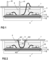
- the power semiconductor module arrangement includes a semiconductor substrate 10.
- the semiconductor substrate 10 includes a dielectric insulation layer 11, a first (structured) metallization layer 111 attached to the dielectric insulation layer 11, and a second (structured) metallization layer 112 attached to the dielectric insulation layer 11.
- the dielectric insulation layer 11 is disposed between the first and the second metallization layer 111, 112. It is, however, also possible that the semiconductor substrate 10 only comprises a first metallization layer 111, while the second metallization layer 112 is omitted.
- the substrate 10 may, e.g., be a Direct Copper Bonding (DCB) substrate, a Direct Aluminum Bonding (DAB) substrate, or an Active Metal Brazing (AMB) substrate.
- the substrate 10 may be an Insulated Metal Substrate (IMS).
- An Insulated Metal Substrate generally comprises a dielectric insulation layer 11 comprising (filled) materials such as epoxy resin or polyimide, for example.
- the material of the dielectric insulation layer 11 may be filled with ceramic particles, for example.
- Such particles may comprise, e.g., Si 2 O, Al 2 O 3 , AlN, or BN and may have a diameter of between about 1 ⁇ m and about 50 ⁇ m.
- an integrated semiconductor substrate is embedded in an AlSiC/magnesium base plate.
- the substrate 10 may also be a conventional printed circuit board (PCB) having a non-ceramic dielectric insulation layer 11.
- PCB printed circuit board
- a non-ceramic dielectric insulation layer 11 may consist of or include a cured resin.
- the semiconductor substrate 10 is arranged in a housing 5.
- the semiconductor substrate 10 forms a ground surface of the housing 5, while the housing 5 itself solely comprises sidewalls. This is, however, only an example. It is also possible that the housing 5 further comprises a ground surface and/or a cover or lid and that the semiconductor substrate 10 is arranged inside the housing 5.
- One or more semiconductor bodies 20 may be arranged on the semiconductor substrate 10.
- Each of the semiconductor bodies 20 arranged on the at least one semiconductor substrate 10 may include a diode, an IGBT (Insulated-Gate Bipolar Transistor), a MOSFET (Metal-Oxide-Semiconductor Field-Effect Transistor), a JFET (Junction Field-Effect Transistor), a HEMT (High-Electron-Mobility Transistor), and/or any other suitable semiconductor element.
- the one or more semiconductor bodies 20 may form a semiconductor arrangement on the semiconductor substrate 10. In Figure 1 , only two semiconductor bodies 20 are exemplarily illustrated.
- the second metallization layer 112 of the semiconductor substrate 10 in Figure 1 is a continuous layer.
- the first metallization layer 111 is a structured layer in the arrangement illustrated in Figure 1 .
- "Structured layer” means that the first metallization layer 111 is not a continuous layer, but includes recesses between different sections of the layer. Such recesses are schematically illustrated in Figure 1 .
- the first metallization layer 111 in this arrangement includes three different sections. Different semiconductor bodies 20 may be mounted on the same or to different sections of the first metallization layer 111.
- first electrical connections 3 such as, e.g., bonding wires, bonding ribbons, ultrasonic welding terminals or joints, or soldered clip connections.
- First electrical connections 3 may also include connection plates or conductor rails, for example, to name just a few examples.
- the one or more semiconductor bodies 20 may be electrically and mechanically connected to the semiconductor substrate 10 by an electrically conductive connection layer 30.
- Such an electrically conductive connection layer 30 may be a solder layer, a layer of an electrically conductive adhesive, or a layer of a sintered metal powder, e.g., silver, for example.
- the power semiconductor module arrangement illustrated in Figure 1 further includes first terminal elements 41.
- the first terminal elements 41 are electrically connected to the first metallization layer 111 and provide an electrical connection between the semiconductor substrate 10 and the outside of the housing 5.
- the first terminal elements 41 may be electrically connected to the first metallization layer 111 with a first end, while a second end of the first terminal elements 41 protrudes out of the housing 5.
- the first terminal elements 41 may be electrically contacted from the outside at their second end.
- the second ends of the first terminal elements 41 may be mechanically and electrically connected to an electronic board, e.g., a printed circuit board (PCB) having a dielectric insulation layer, or to a metal sheet 7.
- a metal sheet could be electrically coupled to a certain electrical potential, for example.
- a non-ceramic dielectric insulation layer may consist of or include a cured resin.
- the electronic board or metal sheet 7 forms a cover of the housing and may comprise through holes. The first terminal elements 41 may be inserted into the through holes of the electronic board or metal sheet 7.
- An electronic board 7 may comprise conducting tracks (not specifically illustrated) arranged on the dielectric insulation layer and a terminal element 41 may be electrically coupled to one or more other first terminal elements 41 by means of one or more such conducting tracks of the electronic board 7.
- a metal sheet generally is also electrically conducting. In this way, an electrical connection may be provided between different sections of the first metallization layer 111, between different semiconductor bodies 20, and/or between any other components that are arranged on the semiconductor substrate 10.
- the first terminal elements 41 may be soldered to the electronic board or metal sheet 7, for example, to provide for a permanent and solid connection. This, however, is only an example.
- the power semiconductor module arrangement may comprise second terminal elements 43.
- Such second terminal elements 43 may be electrically and mechanically connected to the electronic board or metal sheet 7 with a first end, while a second end of the second terminal elements 43 protrudes from the electronic board or metal sheet 7.
- Second terminal elements 43 allow to electrically contact the power semiconductor module arrangement from outside the housing 5. However, contrary to the first terminal elements 41, the second terminal elements do not extend through the electronic board or metal sheet 7 towards the semiconductor substrate 10.
- the second terminal elements 43 terminate on the electronic board or metal sheet 7.
- a second terminal element 43 may be electrically coupled to a conductor track of the electronic board or to the metal sheet 7, for example.
- An electrical connection between the respective conductor track or the metal sheet and the semiconductor substrate 10 may be established by means of one or more of the first terminal elements or by one or more second electrical connections 42, as will be described in the following.
- the power semiconductor module arrangement alternatively or additionally may include second electrical connections 42.
- Such second electrical connections 42 may also provide an electrical connection between the semiconductor substrate 10 and the electronic board or metal sheet 7, and may or may not protrude through the electronic board or metal sheet 7 to the outside of the housing 5.
- the second electrical connection 42 in Figure 1 may comprise a bonding wire or bonding ribbon, for example. A first end of a bonding wire or ribbon is soldered (or welded) to the semiconductor substrate 10, and a second end of a bonding wire or ribbon is soldered (or welded) to the electronic board or metal sheet 7.
- a spring contact may be used, for example, which is pre-assembled and soldered (or welded) to the semiconductor substrate 10 afterwards. If the second electrical connection 42 protrudes through the electronic board or metal sheet 7 to the outside of the housing 5, the second electrical connection 42 may extend through an opening in the electronic board or metal sheet 7 to the outside of the housing 5, for example.
- the housing 5 may be at least partly filled with a sealing resin 8.
- the sealing resin 8 may include a (filled) epoxy resin, silicone gel or other resin materials, for example.
- the sealing resin 8 is configured to seal the components of the power semiconductor module such as the semiconductor substrate 10, in particular the metal patterns formed by the first metallization layer 111, the semiconductor bodies 20, the first electrical connections 3, the first terminal elements 41, and the second electrical connections 42, to provide for insulation and protection of the devices.
- the sealing resin 8 may protect the components from certain environmental conditions and from mechanical damage.
- the sealing resin 8 may at least partly fill the interior of the housing 5, thereby covering the components and electrical connections that are arranged on the semiconductor substrate 10.
- the first terminal elements 41 and the second electrical connections 42 may be partly embedded in the sealing resin 8. At least the second ends of the first terminal elements 41 and of the second electrical connections 42, however, are not covered by the sealing resin 8 and protrude from the sealing resin 8 to the electronic board or metal sheet 7.
- the power semiconductor module may further include a base plate 6.
- the semiconductor substrate 10 may be connected to the base plate 6 via a connection layer (not illustrated).
- a connection layer may be a solder layer, a layer of an adhesive, or a layer of a sintered metal powder, e.g., silver, for example.
- Figure 1 schematically illustrates a power semiconductor arrangement with a base plate 6.
- the base plate 6 may be omitted.
- the semiconductor substrate 10 may form a ground surface of the housing 5, for example.
- the semiconductor substrate 10, instead of on a base plate 6, may be arranged on a heat sink, for example.
- the power semiconductor module arrangement comprises a base plate 6, the base plate 6 may also further be arranged on a heat sink (heat sink not specifically illustrated) such that the base plate 6 is arranged between the heat sink and the semiconductor substrate 10, for example.
- more than one semiconductor substrate 10 is arranged on a single base plate 6. Irrespective of the number of semiconductor substrates 10 that are mounted on the base plate 6, the base plate 6 may form a ground surface of the housing 5, for example.
- Semiconductor bodies 20 may be arranged on one or more of a plurality of semiconductor substrates 10.
- the one or more semiconductor substrates 10 are assembled first. That is, the first metallization layer 111 and, optionally, the second metallization layer 112 are formed on the dielectric insulation layer 11, and one or more semiconductor bodies 20 are arranged on the semiconductor substrate 10. Assembly of the one or more semiconductor substrates 10 further comprises forming the first electrical connections 3 on the semiconductor substrates 10. Any other elements of a power semiconductor module arrangement may be mounted onto the semiconductor substrate 10 as well during the assembly process. Once the at least one semiconductor substrate 10 is fully assembled, it may be arranged in a housing 5. An electronic board having conductor tracks formed thereon or a metal sheet 7 may then be provided. During or shortly before mounting the electronic board or metal sheet 7 onto the housing 5, the second electrical connections 42 may be formed.
- a first end of a second electrical connection 42 (e.g., bonding wire or ribbon) may be mounted onto one of the at least one semiconductor substrate 10.
- the electronic board or metal sheet 7 may then be arranged close to the housing 5, but not yet fully covering the housing 5, in order to be able to couple the second end of the second electrical connection 42 to the electronic board or metal sheet 7.
- the electronic board or metal sheet 7 may be mounted and fixed onto the housing 5, thereby forming a cover of the housing 5, for example.
- second electrical connections 42 in particular forming a connection between the second ends and the electronic board or metal sheet 7 may be challenging.
- the electronic board or metal sheet 7 needs to be firmly held in place and prevented from vibrating.
- second electrical connections 42 are defective or that second electrical connections 42 are torn off during the process of mounting the electronic board or metal sheet 7 onto the housing 5. Therefore, second electrical connections 42 that electrically couple a semiconductor substrate 10 to an electronic board or metal sheet 7 in the described manner are often designed redundantly. That is, two or more second electrical connections 42 may be used to form a single connection. In this way, the number of defects may be reduced and the reliability of the power semiconductor module arrangement may be increased.
- the overall costs for the power semiconductor module increase, as more electrical connections are required. This results in an increase of material usage, as well as in increased space requirements.
- a power semiconductor module arrangement according to one example is schematically illustrated.
- the power semiconductor module arrangement essentially corresponds to the arrangement illustrated in Figure 1 .
- First and second terminal elements 41, 43 are not specifically illustrated in Figure 2 .
- the at least one second electrical connection 42 differs from the second electrical connection 42 as discussed with respect to Figure 1 above.
- one second electrical connection 42 is exemplarily illustrated.
- a power semiconductor module arrangement may comprise a plurality of second electrical connections 42 in order to electrically couple various sections of the first metallization layer 111 and various conducting paths of the electronic board 7, or various sections of the first metallization layer 111 and the metal sheet 7 to each other.
- the second electrical connection 42 illustrated in Figure 2 comprises a first end 421 that is mechanically coupled to the electronic board or metal sheet 7, and a second end 422 that is mechanically coupled to the electronic board or metal sheet 7 distant to the first end 421.
- the first end 421 may be electrically coupled to a first conductor track of an electronic board 7, for example.
- the second end 422 may be electrically coupled to the first or to a second conductor track of the electronic board 7, for example.
- the different first and the second conductor tracks may be coupled to the same electrical potential.
- the second electrical connection 42 further comprises an intermediate section extending between the first end 421 and the second end 422.
- the intermediate section is mechanically coupled to the semiconductor substrate 10.
- a middle section 423 of the intermediate section may be mechanically coupled to the semiconductor substrate 10.
- a middle section 423 of the intermediate section is a section that is arranged essentially centrally between the first end 421 and the second end 422. That is, a distance from the middle section 423 to the first end 421 essentially equals a distance between the middle section 423 and the second end 422.
- the intermediate section of the second electrical connection 42 may form an arc, bridge or loop between the first end 421 and the second end 422. That is, the intermediate section extends from the first end 421 and the second end 422 towards the semiconductor substrate 10, when the power semiconductor module arrangement is fully assembled.
- the middle section 423 of the intermediate section may form the topmost point (or undermost point) of the arc, bridge or loop. That is, the middle section 423 may form that part of the intermediate section that is arranged the farthest away from the electronic board or metal sheet 7 and the closest to the semiconductor substrate 10 when the power semiconductor module arrangement is fully assembled.
- the arc, bridge or loop formed by the intermediate section may have an offset that may give way when connecting the middle section 423 to the semiconductor substrate 10.
- the arc, bridge or loop formed by the intermediate section may have a rounded form, as is schematically illustrated in Figure 2 .
- the arc, bridge or loop has an angular form. That is, the intermediate section may have comparably sharp corners, in particular near the middle section 423.
- the intermediate section may have any suitable form.
- the second electrical connection 42 illustrated in Figure 2 and described above is a very stable connection.
- the second electrical connection 42 comprises two points of contact connecting the second electrical connection 42 to the electronic board or metal sheet 7, and a further point of contact connecting the second electrical connection 42 to the semiconductor substrate 10.
- This makes a redundant design superfluous. That is, there is no need to provide two identical second electrical connections 42 for the same electrical interconnection between the semiconductor substrate 10 and the electronic board or metal sheet 7.
- the overall costs as well as the space requirements and therefore the size of the power semiconductor module arrangement of the example illustrated in Figure 2 therefore, are reduced as compared to the arrangement as illustrated in Figure 1 , which generally requires a redundant design in order to reduce the risk of failures.
- the second electrical connection 42 may comprise a bonding wire or a bonding ribbon.
- Bonding wires generally have a round or rounded (e.g., oval) cross section, while bonding ribbons generally have an angular (e.g., square or rectangular) cross section.
- Bonding wires may have diameters of between 10 ⁇ m and 50 ⁇ m (thin bonding wires), or between 50 ⁇ m and 600 ⁇ m (thick bonding wires), for example. Any other diameters, however, are also possible.
- the diameter of a bonding wire may depend on the material that is used to form the bonding wire, for example.
- the diameter of a bonding wire may further depend on the application the power semiconductor module arrangement is to be used in and the current range of the specific application, for example.
- Dimensions of bonding ribbons may be in the range of 60 x 10 ⁇ m (width x thickness) up to 3000 x 400 ⁇ m, for example. Any other dimensions, however, are also possible.
- the at least one second electrical connection 42 may comprise at least one of Al (aluminum), AlMg (magnesium alloyed aluminum), Cu (copper), and Au (gold), for example. That is, aluminum, aluminum alloyed, copper or gold bonding wires or ribbons may be used to form the second electrical connections 42, for example. According to one example, the at least one second electrical connection 42 comprises an aluminum cladded copper wire.
- the middle section 423 is mechanically and electrically coupled to the semiconductor substrate 10.
- the middle section 423 is mechanically and electronically coupled to other components of the power semiconductor module arrangement.
- the middle section 423 alternatively may be mechanically and electrically coupled to any other suitable components of the power semiconductor module arrangement. It is possible to combine the different options within one and the same power semiconductor module arrangement.
- a first group of second electrical connections 42 may be mechanically end electrically coupled to the semiconductor substrate 10, while another group of second electrical connections 42 may be mechanically and electrically coupled to a semiconductor body 20 or any other component of the power semiconductor module arrangement.
- Each group of second electrical connections 42 may comprise one or more of a plurality of second electrical connections 42.
- a second electrical connection 42 may be mounted onto an electronic board or metal sheet 7. That is, a first end 421 and a second end 422 of an electrical connection 42 may be mechanically (and electrically) coupled to the electronic board or metal sheet 7.
- the connections between the first and second ends 421, 422 and the electronic board or metal sheet 7 may be formed by means of a bonding, a welding, or an ultrasonic bonding or welding process, for example. Such processes are generally known and will not be described in further detail herein.
- the first side of the electronic board or metal sheet 7 may face the semiconductor substrate 10. That is, the first side of the electronic board or metal sheet 7 may face a first side of the semiconductor substrate 10, wherein the first side of the semiconductor substrate 10 is a side on which at least one semiconductor body 20 is arranged (see, e.g., Figures 2 and 3 ).
- a distance d1 between the electronic board or metal sheet 7 and the semiconductor substrate 10 may equal or be slightly less than a height d2 of the arc, bridge or loop formed by the intermediate section of the second electrical connection 42.
- the height d2 of the arc, bridge or loop may equal a distance between the middle section 423 and the electronic board or metal sheet 7 (see Figure 5 ). That is, when arranging the electronic board or metal sheet 7 with the second electrical connection 42 mounted thereon above the semiconductor substrate 10, the middle section 423 of the second electronic connection 42 loosely contacts the semiconductor substrate 10, the semiconductor body 20, or any other component of the power semiconductor module arrangement.
- the electronic board or metal sheet 7 comprises a though hole 71.
- the first end 421 of the second electronic connection 42 is arranged on a first side of the through hole 71, and the second end 422 of the second electronic connection 42 is arranged on a second side of the through hole 71, wherein the second side is opposite to the first side.
- a connection tool 90 e.g., bonding or welding tool
- connection tool 90 vibrates at a certain frequency.
- the through hole 71 allows an easy access of the connection tool 90 towards the middle section 423. In this way, a very stable connection may be formed between the second electrical connection 42 and the semiconductor substrate 10, semiconductor body 20 or other component in an easy and convenient way even if the electronic board or metal sheet 7 is already arranged in its final mounted position. That is, the electronic board or metal sheet 7 remains in its position after forming the connections between the middle sections 423 and the semiconductor substrate 10, semiconductor body 20, or other component.
- the electronic board or metal sheet 7 may comprise a plurality of through holes 71.
- the number of through holes 71 may be equal to or greater than the number of second electrical connections 42. That is, each second electrical connection 42 may be arranged on the electronic board or metal sheet 7 such that its middle section 423 extends over a different one of the through holes 71. This allows to mechanically couple each of the second electrical connections 42 to the semiconductor substrate 10, semiconductor body 20, or other component after arranging the electronic board or metal sheet 7 above the semiconductor substrate 10.
- any additional through holes 71 may serve different purposes, for example.
- lead frames 41 may extend through any additional through holes 71. This, however, is optional.
- a method for producing a power semiconductor module arrangement may comprise assembling the semiconductor substrate 10 before arranging the electronic board or metal sheet 7 above the semiconductor substrate 10. The step of assembling the semiconductor substrate 10 has already been discussed exemplarily above.
- a method for producing a power semiconductor module arrangement may further comprise arranging the semiconductor substrate 10 in a housing 5.
- a housing 5 is not illustrated in the example of Figure 4 .
- the semiconductor substrate 10 may be fully assembled when it is arranged in the housing 5, for example.
- the electronic board or metal sheet 7 may then be arranged in or on the housing 5.
- the electronic board or metal sheet 7 may be arranged on the sidewalls of the housing 5. A height of the sidewalls in this case may define the distance d1 between the electronic board or metal sheet 7 and the semiconductor substrate 10.
- the electronic board or metal sheet 7 may be fixed to the sidewalls of the housing 5 in any suitable way (e.g., insert, gluing, screwing or clamping). It is also possible that the sidewalls of the housing 5 comprise projections on the inside of the housing 5. The electronic board or metal sheet 7 may be arranged inside the housing 5, resting on such projections, for example. In this way, the electronic board or metal sheet 7 may be precisely aligned with respect to the layout of the semiconductor substrate 10. An additional adhesion or clamping in order to fix the electronic board or metal sheet 7 in its position may not even be necessary in many cases.
- the mechanical (and electrical) connections between the middle sections 423 of the at least one second electrical connection 42 and the semiconductor substrate 10, semiconductor body 20 or other component may then be easily formed by inserting the connection tool 90 through the respective through holes 71.
- the electronic board or metal sheet 7 forms a cover of the housing 5.
- an additional cover may be mounted on the sidewalls such that the electronic board or metal sheet 7 is arranged inside the housing 5 and is not directly accessible from the outside of the housing.
- second electrical connections 42 allow the usage of the power semiconductor module arrangement for applications having a voltage class of even above 3.3kV. The risk of failures is reduced as compared to conventional arrangements.
- the second electrical connection 42 comprises a first end 421 that is coupled to the electronic board or metal sheet 7.
- the second electrical connection 42 further comprises a second end 422 that is coupled to the electronic board or metal sheet 7.
- the first and second ends 421, 422 are arranged on opposite sides of a though hole 71 on the same side of the electronic board or metal sheet 7.
- a distance e between the first end 421 and the second end 422 may be larger than a width a of the through hole 71 in the same direction. That is, the first and second ends 421, 422 may not directly adjoin the though hole 71.
- first end and the second end 421, 422 each are arranged at a certain distance from the outer diameter of the through hole 71. This distance may depend on the dimensions of the second electrical connection 42 as well as on the distance between the electronic board or metal sheet 7 and the semiconductor substrate 10, semiconductor body 20 or other component in the fully assembled power semiconductor module arrangement.
- the intermediate section of the second electronic connection 42 extends from the electronic board or metal sheet 7 and forms an arc, bridge or loop that extends from the first end 421 over the through hole 71 to the second end 422.
- the middle section 423 is arranged directly above the through hole 71 to be accessible by a connection tool 90.
- the dimensions a of the through hole 71 generally depend on the size of the connection tool 90 that is used to form the connection between the middle section 423 and the semiconductor substrate 10, semiconductor body 20, or other component.
- the through hole 71 is large enough in order to allow the connection tool 90 to easily access the middle section 423.
- the dimensions a of the through hole 71 may further allow vibrations of the connection tool 90. That is, even when vibrating during the connection process, the connection tool 90 may not touch the electronic board or metal sheet 7. Therefore, no vibrations may be transferred from the connection tool 90 to the electronic board or metal sheet 7.
- An angle f between the first end 421 and the intermediate section generally depends on the height d2 of the arc, bridge or loop as well as on the dimensions a of the through hole 71.
- the dimension c (e.g., diameter) of the electrical connection 42 (e.g., bonding wire or bonding ribbon) has already been discussed above.
- the height d2 of the arc may depend on the distance e between the first end 421 and the second end 422 as well as on the angles f, g between the first and second ends 421, 422 and the intermediate section.
- the shape of the arc, bridge or loop formed by the intermediate section of the second electrical connection 42 may vary depending on the size and dimensions of the power semiconductor module arrangement and its components in order to be able to give way (elasticity) when connecting the middle section 423 to the semiconductor substrate 10, semiconductor body 20 or other component to prevent damage to the previously formed contacts between the first end 421 and the second end 422 and the electronic board or metal sheet 7.
Landscapes
- Engineering & Computer Science (AREA)
- Microelectronics & Electronic Packaging (AREA)
- Power Engineering (AREA)
- Computer Hardware Design (AREA)
- Physics & Mathematics (AREA)
- Condensed Matter Physics & Semiconductors (AREA)
- General Physics & Mathematics (AREA)
- Chemical & Material Sciences (AREA)
- Ceramic Engineering (AREA)
- Materials Engineering (AREA)
- Cooling Or The Like Of Semiconductors Or Solid State Devices (AREA)
- Combinations Of Printed Boards (AREA)
Claims (13)
- Leistungshalbleitermodulanordnung, umfassend:ein Halbleitersubstrat (10), das in einem Gehäuse (5) angeordnet ist, wobei auf dem Halbleitersubstrat (10) ein oder mehrere Elemente montiert sind;eine Elektronikplatine oder ein Metallblech (7), das in dem Gehäuse (5) in einem Abstand zu dem Halbleitersubstrat (10) angeordnet ist, wobei die Elektronikplatine oder das Metallblech (7) parallel zu dem Halbleitersubstrat (10) angeordnet ist; undmindestens eine elektrische Verbindung (42), die dazu ausgelegt ist, die Elektronikplatine oder das Metallblech (7) elektrisch mit dem Halbleitersubstrat (10) oder einem der darauf montierten Elemente zu koppeln, wobei jede der mindestens einen elektrischen Verbindung (42) ein erstes Ende (421) und ein zweites Ende (422) und einen zwischen dem ersten Ende (421) und dem zweiten Ende (422) verlaufenden Zwischenabschnitt umfasst, und wobei das erste Ende (421) und das zweite Ende (422) jeder elektrischen Verbindung (42) mechanisch mit der Elektronikplatine oder dem Metallblech (7) gekoppelt sind und ein Mittelabschnitt (423) des Zwischenabschnitts mechanisch mit dem Halbleitersubstrat (10) oder einem der darauf montierten Elemente gekoppelt ist, dadurch gekennzeichnet, dass die Elektronikplatine oder das Metallblech (7) einen Deckel des Gehäuses (5) bildet.
- Leistungshalbleitermodulanordnung nach Anspruch 1, wobei der Zwischenabschnitt jeder elektrischen Verbindung (42) einen Bogen, eine Brücke oder eine Schleife zwischen dem ersten Ende (421) und dem zweiten Ende (422) der jeweiligen elektrischen Verbindung (42) bildet.
- Leistungshalbleitermodulanordnung nach Anspruch 2, wobei der Mittelabschnitt (423) mittig zwischen dem ersten Ende (421) und dem zweiten Ende (422) am höchsten Punkt des Bogens, der Brücke oder der Schleife angeordnet ist und einen Abschnitt der zweiten elektrischen Verbindung (42) darstellt, der am weitesten von der Elektronikplatine oder dem Metallblech (7) entfernt angeordnet ist.
- Leistungshalbleitermodulanordnung nach einem der Ansprüche 1 bis 3, wobei die Elektronikplatine oder das Metallblech (7) mindestens ein Durchgangsloch (71) umfasst und wobei für jede der mindestens einen elektrischen Verbindung (42)das erste Ende (421) auf einer ersten Seite eines des mindestens einen Durchgangslochs (71) angeordnet ist; das zweite Ende (422) auf einer zweiten Seite des jeweiligen Durchgangslochs (71) angeordnet ist, wobei die zweite Seite der ersten Seite gegenüberliegt; undder Zwischenabschnitt über das Durchgangsloch (71) hinweg verläuft.
- Leistungshalbleitermodulanordnung nach einem der Ansprüche 1 bis 4, wobei jede der mindestens einen elektrischen Verbindung (42) einen Bonddraht oder ein Bondband umfasst.
- Leistungshalbleitermodulanordnung nach einem der Ansprüche 1 bis 5, wobei jede der mindestens einen elektrischen Verbindung (42) mindestens eines von Al, AlMg, Cu und Au oder einen aluminiumumkaschierten Kupferdraht umfasst.
- Leistungshalbleitermodulanordnung nach einem der Ansprüche 1 bis 6, wobei eine mechanische Verbindung zwischen dem ersten Ende (421) und der Elektronikplatine oder dem Metallblech (7), zwischen dem zweiten Ende (422) und der Elektronikplatine oder dem Metallblech (7) und zwischen dem Mittelabschnitt (423) und dem Halbleitersubstrat (10) oder dem darauf montierten Element eine Bondverbindung oder eine Schweißverbindung ist.
- Leistungshalbleitermodulanordnung nach einem der vorhergehenden Ansprüche, wobei das mindestens eine Element mindestens einen Halbleiterkörper (20) umfasst, der auf einer ersten Oberfläche des Halbleitersubstrats (10) montiert ist.
- Leistungshalbleitermodulanordnung nach Anspruch 8, wobei die mindestens eine elektrische Verbindung (42) auf einer ersten Oberfläche der Elektronikplatine oder des Metallblechs (7) angeordnet ist und wobei die erste Oberfläche der Elektronikplatine oder des Metallblechs (7) der ersten Oberfläche des Halbleitersubstrats (10) zugewandt ist.
- Verfahren zur Herstellung einer Halbeitermodulanordnung, wobei das Verfahren Folgendes umfasst:Montieren mindestens einer elektrischen Verbindung (42) auf einer Elektronikplatine oder einem Metallblech (7) durch Verbinden eines ersten Endes (421) und eines zweiten Endes (422) der elektrischen Verbindung (42) mit einer ersten Seite der Elektronikplatine oder des Metallblechs (7);Anordnen der Elektronikplatine oder des Metallblechs (7) mit der darauf montierten elektrischen Verbindung (42) parallel zu einem Halbleitersubstrat (10) so, dass die erste Seite der Elektronikplatine oder des Metallblechs (7) dem Halbleitersubstrat (10) zugewandt ist, wobei das Halbleitersubstrat (10) ein oder mehrere darauf montierte Elemente aufweist; undVerbinden eines mittleren Abschnitts (423) eines Zwischenabschnitts der elektrischen Verbindung (42) mit dem Halbleitersubstrat (10) oder mit einem der darauf montierten Elemente, wobei sich der Zwischenabschnitt zwischen dem ersten Ende (421) und dem zweiten Ende (422) der elektrischen Verbindung (42) erstreckt, wobei die Elektronikplatine oder das Blech (7) als Deckel des Gehäuses (5) angeordnet ist.
- Verfahren nach Anspruch 10, wobei das Verbinden des mittleren Abschnitts (423) des Zwischenabschnitts der elektrischen Verbindung (42) mit dem Halbleitersubstrat (10) oder mit einem der darauf montierten Elemente das Einführen eines Verbindungswerkzeugs (90) durch ein Durchgangsloch (71) der Elektronikplatine oder des Metallblechs (7) und das Pressen des mittleren Abschnitts (423) auf das Halbleitersubstrat (10) oder auf eines der darauf montierten Elemente umfasst.
- Verfahren nach Anspruch 10 oder 11, ferner umfassend, vor dem Anordnen der Elektronikplatine oder des Metallblechs (7) mit der darauf montierten elektrischen Verbindung (42) parallel zu einem Halbleitersubstrat (10) das Anordnen des Halbleitersubstrats (10) in einem Gehäuse (5).
- Verfahren nach Anspruch 12, wobei das Anordnen der Elektronikplatine oder des Metallblechs (7) mit der darauf montierten elektrischen Verbindung (42) parallel zu einem Halbleitersubstrat (10) das Anordnen der Elektronikplatine oder des Metallblechs (7) in oder auf dem Gehäuse (5) umfasst.
Priority Applications (1)
| Application Number | Priority Date | Filing Date | Title |
|---|---|---|---|
| EP20155372.4A EP3863045B1 (de) | 2020-02-04 | 2020-02-04 | Leistungshalbleitermodulanordnung und verfahren zur herstellung davon |
Applications Claiming Priority (1)
| Application Number | Priority Date | Filing Date | Title |
|---|---|---|---|
| EP20155372.4A EP3863045B1 (de) | 2020-02-04 | 2020-02-04 | Leistungshalbleitermodulanordnung und verfahren zur herstellung davon |
Publications (2)
| Publication Number | Publication Date |
|---|---|
| EP3863045A1 EP3863045A1 (de) | 2021-08-11 |
| EP3863045B1 true EP3863045B1 (de) | 2025-05-21 |
Family
ID=69468427
Family Applications (1)
| Application Number | Title | Priority Date | Filing Date |
|---|---|---|---|
| EP20155372.4A Active EP3863045B1 (de) | 2020-02-04 | 2020-02-04 | Leistungshalbleitermodulanordnung und verfahren zur herstellung davon |
Country Status (1)
| Country | Link |
|---|---|
| EP (1) | EP3863045B1 (de) |
Families Citing this family (2)
| Publication number | Priority date | Publication date | Assignee | Title |
|---|---|---|---|---|
| CN113658934A (zh) * | 2021-08-23 | 2021-11-16 | 无锡利普思半导体有限公司 | 功率模块内部连接铜片及其制备方法、功率半导体模块 |
| EP4174928A1 (de) * | 2021-10-28 | 2023-05-03 | Siemens Aktiengesellschaft | Halbleiterbauelement mit gedämpften bondflächen in einem gehäuse mit umspritzten pins |
Family Cites Families (4)
| Publication number | Priority date | Publication date | Assignee | Title |
|---|---|---|---|---|
| JP2009231685A (ja) * | 2008-03-25 | 2009-10-08 | Mitsubishi Electric Corp | パワー半導体装置 |
| CN105765715B (zh) * | 2013-11-26 | 2018-08-03 | 三菱电机株式会社 | 功率模块以及功率模块的制造方法 |
| JP2016099127A (ja) * | 2014-11-18 | 2016-05-30 | 富士電機株式会社 | パワー半導体モジュールの製造方法及びその中間組立ユニット |
| US9508658B1 (en) * | 2015-08-05 | 2016-11-29 | Macom Technology Solutions Holdings, Inc. | Electromagnetic wall in millimeter-wave cavity |
-
2020
- 2020-02-04 EP EP20155372.4A patent/EP3863045B1/de active Active
Also Published As
| Publication number | Publication date |
|---|---|
| EP3863045A1 (de) | 2021-08-11 |
Similar Documents
| Publication | Publication Date | Title |
|---|---|---|
| US8018047B2 (en) | Power semiconductor module including a multilayer substrate | |
| US7679914B2 (en) | Electronic controller | |
| US12041755B2 (en) | Power semiconductor module arrangement and method for producing a power semiconductor module arrangement | |
| EP1466357B1 (de) | Gehäuse zur oberflächenanbringung mit von der trägerplatte beabstandetem chipboden | |
| US11942449B2 (en) | Semiconductor arrangement and method for producing the same | |
| CN100562999C (zh) | 电路模块 | |
| US11581230B2 (en) | Power semiconductor module and a method for producing a power semiconductor module | |
| EP3499649A1 (de) | Leistungshalbleitermodulanordnung | |
| EP3863045B1 (de) | Leistungshalbleitermodulanordnung und verfahren zur herstellung davon | |
| JPH06177295A (ja) | 混成集積回路装置 | |
| EP3644358A1 (de) | Leistungshalbleitermodulanordnung mit einem kontaktelement | |
| US11282774B2 (en) | Power semiconductor module arrangement | |
| JPH08148647A (ja) | 半導体装置 | |
| JP3297959B2 (ja) | 半導体装置 | |
| EP4510184A1 (de) | Anschlusselement und leistungshalbleitermodulanordnung mit einem anschlusselement | |
| EP4365935A1 (de) | Leistungshalbleitermodulanordnung | |
| EP4270466A1 (de) | Leistungshalbleitermodulanordnungen und verfahren zum produzieren von leistungshalbleitermodulanordnungen | |
| EP4345884A1 (de) | Leistungshalbleitermodulanordnung und leiterplatte für eine leistungshalbleitermodulanordnung | |
| EP4411995A1 (de) | Verfahren zur bildung eines anschlusselements, anschlusselement und leistungshalbleitermodulanordnung mit einem anschlusselement | |
| US20240162099A1 (en) | Power semiconductor module arrangement and method for assembling the same | |
| CN114975288A (zh) | 功率半导体模块装置 | |
| JPH0864719A (ja) | 混成集積回路 | |
| JPH11145378A (ja) | 複合電子回路装置 | |
| JP2001313352A (ja) | 半導体装置及びその製造方法 | |
| JPH0364051A (ja) | 半導体装置 |
Legal Events
| Date | Code | Title | Description |
|---|---|---|---|
| PUAI | Public reference made under article 153(3) epc to a published international application that has entered the european phase |
Free format text: ORIGINAL CODE: 0009012 |
|
| STAA | Information on the status of an ep patent application or granted ep patent |
Free format text: STATUS: THE APPLICATION HAS BEEN PUBLISHED |
|
| AK | Designated contracting states |
Kind code of ref document: A1 Designated state(s): AL AT BE BG CH CY CZ DE DK EE ES FI FR GB GR HR HU IE IS IT LI LT LU LV MC MK MT NL NO PL PT RO RS SE SI SK SM TR |
|
| STAA | Information on the status of an ep patent application or granted ep patent |
Free format text: STATUS: REQUEST FOR EXAMINATION WAS MADE |
|
| 17P | Request for examination filed |
Effective date: 20220210 |
|
| RBV | Designated contracting states (corrected) |
Designated state(s): AL AT BE BG CH CY CZ DE DK EE ES FI FR GB GR HR HU IE IS IT LI LT LU LV MC MK MT NL NO PL PT RO RS SE SI SK SM TR |
|
| REG | Reference to a national code |
Ref country code: DE Ref legal event code: R079 Ref country code: DE Ref legal event code: R079 Ref document number: 602020051487 Country of ref document: DE Free format text: PREVIOUS MAIN CLASS: H01L0023000000 Ipc: H01L0023373000 |
|
| GRAP | Despatch of communication of intention to grant a patent |
Free format text: ORIGINAL CODE: EPIDOSNIGR1 |
|
| STAA | Information on the status of an ep patent application or granted ep patent |
Free format text: STATUS: GRANT OF PATENT IS INTENDED |
|
| RIC1 | Information provided on ipc code assigned before grant |
Ipc: H01L 25/16 20060101ALI20241220BHEP Ipc: H01L 23/00 20060101ALI20241220BHEP Ipc: H01L 25/07 20060101ALI20241220BHEP Ipc: H01L 23/538 20060101ALI20241220BHEP Ipc: H01L 23/498 20060101ALI20241220BHEP Ipc: H01L 23/373 20060101AFI20241220BHEP |
|
| INTG | Intention to grant announced |
Effective date: 20250121 |
|
| P01 | Opt-out of the competence of the unified patent court (upc) registered |
Free format text: CASE NUMBER: APP_10084/2025 Effective date: 20250227 |
|
| GRAS | Grant fee paid |
Free format text: ORIGINAL CODE: EPIDOSNIGR3 |
|
| GRAA | (expected) grant |
Free format text: ORIGINAL CODE: 0009210 |
|
| STAA | Information on the status of an ep patent application or granted ep patent |
Free format text: STATUS: THE PATENT HAS BEEN GRANTED |
|
| AK | Designated contracting states |
Kind code of ref document: B1 Designated state(s): AL AT BE BG CH CY CZ DE DK EE ES FI FR GB GR HR HU IE IS IT LI LT LU LV MC MK MT NL NO PL PT RO RS SE SI SK SM TR |
|
| REG | Reference to a national code |
Ref country code: GB Ref legal event code: FG4D |
|
| REG | Reference to a national code |
Ref country code: CH Ref legal event code: EP |
|
| REG | Reference to a national code |
Ref country code: DE Ref legal event code: R096 Ref document number: 602020051487 Country of ref document: DE |
|
| REG | Reference to a national code |
Ref country code: IE Ref legal event code: FG4D |
|
| REG | Reference to a national code |
Ref country code: NL Ref legal event code: MP Effective date: 20250521 |
|
| PG25 | Lapsed in a contracting state [announced via postgrant information from national office to epo] |
Ref country code: PT Free format text: LAPSE BECAUSE OF FAILURE TO SUBMIT A TRANSLATION OF THE DESCRIPTION OR TO PAY THE FEE WITHIN THE PRESCRIBED TIME-LIMIT Effective date: 20250922 Ref country code: FI Free format text: LAPSE BECAUSE OF FAILURE TO SUBMIT A TRANSLATION OF THE DESCRIPTION OR TO PAY THE FEE WITHIN THE PRESCRIBED TIME-LIMIT Effective date: 20250521 Ref country code: ES Free format text: LAPSE BECAUSE OF FAILURE TO SUBMIT A TRANSLATION OF THE DESCRIPTION OR TO PAY THE FEE WITHIN THE PRESCRIBED TIME-LIMIT Effective date: 20250521 |
|
| REG | Reference to a national code |
Ref country code: LT Ref legal event code: MG9D |
|
| PG25 | Lapsed in a contracting state [announced via postgrant information from national office to epo] |
Ref country code: GR Free format text: LAPSE BECAUSE OF FAILURE TO SUBMIT A TRANSLATION OF THE DESCRIPTION OR TO PAY THE FEE WITHIN THE PRESCRIBED TIME-LIMIT Effective date: 20250822 Ref country code: NO Free format text: LAPSE BECAUSE OF FAILURE TO SUBMIT A TRANSLATION OF THE DESCRIPTION OR TO PAY THE FEE WITHIN THE PRESCRIBED TIME-LIMIT Effective date: 20250821 |
|
| PG25 | Lapsed in a contracting state [announced via postgrant information from national office to epo] |
Ref country code: NL Free format text: LAPSE BECAUSE OF FAILURE TO SUBMIT A TRANSLATION OF THE DESCRIPTION OR TO PAY THE FEE WITHIN THE PRESCRIBED TIME-LIMIT Effective date: 20250521 Ref country code: PL Free format text: LAPSE BECAUSE OF FAILURE TO SUBMIT A TRANSLATION OF THE DESCRIPTION OR TO PAY THE FEE WITHIN THE PRESCRIBED TIME-LIMIT Effective date: 20250521 |
|
| PG25 | Lapsed in a contracting state [announced via postgrant information from national office to epo] |
Ref country code: BG Free format text: LAPSE BECAUSE OF FAILURE TO SUBMIT A TRANSLATION OF THE DESCRIPTION OR TO PAY THE FEE WITHIN THE PRESCRIBED TIME-LIMIT Effective date: 20250521 |
|
| PG25 | Lapsed in a contracting state [announced via postgrant information from national office to epo] |
Ref country code: HR Free format text: LAPSE BECAUSE OF FAILURE TO SUBMIT A TRANSLATION OF THE DESCRIPTION OR TO PAY THE FEE WITHIN THE PRESCRIBED TIME-LIMIT Effective date: 20250521 |
|
| PG25 | Lapsed in a contracting state [announced via postgrant information from national office to epo] |
Ref country code: RS Free format text: LAPSE BECAUSE OF FAILURE TO SUBMIT A TRANSLATION OF THE DESCRIPTION OR TO PAY THE FEE WITHIN THE PRESCRIBED TIME-LIMIT Effective date: 20250821 |
|
| PG25 | Lapsed in a contracting state [announced via postgrant information from national office to epo] |
Ref country code: IS Free format text: LAPSE BECAUSE OF FAILURE TO SUBMIT A TRANSLATION OF THE DESCRIPTION OR TO PAY THE FEE WITHIN THE PRESCRIBED TIME-LIMIT Effective date: 20250921 |
|
| PG25 | Lapsed in a contracting state [announced via postgrant information from national office to epo] |
Ref country code: LV Free format text: LAPSE BECAUSE OF FAILURE TO SUBMIT A TRANSLATION OF THE DESCRIPTION OR TO PAY THE FEE WITHIN THE PRESCRIBED TIME-LIMIT Effective date: 20250521 |
|
| REG | Reference to a national code |
Ref country code: DE Ref legal event code: R079 Ref document number: 602020051487 Country of ref document: DE Free format text: PREVIOUS MAIN CLASS: H01L0023373000 Ipc: H10W0040250000 |
|
| REG | Reference to a national code |
Ref country code: AT Ref legal event code: MK05 Ref document number: 1797553 Country of ref document: AT Kind code of ref document: T Effective date: 20250521 |
|
| PG25 | Lapsed in a contracting state [announced via postgrant information from national office to epo] |
Ref country code: AT Free format text: LAPSE BECAUSE OF FAILURE TO SUBMIT A TRANSLATION OF THE DESCRIPTION OR TO PAY THE FEE WITHIN THE PRESCRIBED TIME-LIMIT Effective date: 20250521 Ref country code: SM Free format text: LAPSE BECAUSE OF FAILURE TO SUBMIT A TRANSLATION OF THE DESCRIPTION OR TO PAY THE FEE WITHIN THE PRESCRIBED TIME-LIMIT Effective date: 20250521 Ref country code: DK Free format text: LAPSE BECAUSE OF FAILURE TO SUBMIT A TRANSLATION OF THE DESCRIPTION OR TO PAY THE FEE WITHIN THE PRESCRIBED TIME-LIMIT Effective date: 20250521 |