EP3853773B1 - Procede de fabrication d'un module electronique pour objet portatif - Google Patents
Procede de fabrication d'un module electronique pour objet portatif Download PDFInfo
- Publication number
- EP3853773B1 EP3853773B1 EP19763008.0A EP19763008A EP3853773B1 EP 3853773 B1 EP3853773 B1 EP 3853773B1 EP 19763008 A EP19763008 A EP 19763008A EP 3853773 B1 EP3853773 B1 EP 3853773B1
- Authority
- EP
- European Patent Office
- Prior art keywords
- electrically conductive
- integrated circuit
- substrate
- electronic module
- connection
- Prior art date
- Legal status (The legal status is an assumption and is not a legal conclusion. Google has not performed a legal analysis and makes no representation as to the accuracy of the status listed.)
- Active
Links
- 238000000034 method Methods 0.000 title claims description 21
- 238000004519 manufacturing process Methods 0.000 title claims description 13
- 239000000758 substrate Substances 0.000 claims description 29
- 239000004020 conductor Substances 0.000 claims description 12
- 229920000139 polyethylene terephthalate Polymers 0.000 claims description 11
- 239000005020 polyethylene terephthalate Substances 0.000 claims description 11
- 239000012790 adhesive layer Substances 0.000 claims description 9
- 239000004800 polyvinyl chloride Substances 0.000 claims description 7
- -1 polyethylene terephthalate Polymers 0.000 claims description 5
- RYGMFSIKBFXOCR-UHFFFAOYSA-N Copper Chemical compound [Cu] RYGMFSIKBFXOCR-UHFFFAOYSA-N 0.000 claims description 4
- 229910052782 aluminium Inorganic materials 0.000 claims description 4
- XAGFODPZIPBFFR-UHFFFAOYSA-N aluminium Chemical compound [Al] XAGFODPZIPBFFR-UHFFFAOYSA-N 0.000 claims description 4
- 229910052802 copper Inorganic materials 0.000 claims description 4
- 239000010949 copper Substances 0.000 claims description 4
- 239000011241 protective layer Substances 0.000 claims description 3
- 239000004411 aluminium Substances 0.000 claims description 2
- 238000005516 engineering process Methods 0.000 description 6
- 239000010410 layer Substances 0.000 description 5
- 239000000853 adhesive Substances 0.000 description 4
- 230000001070 adhesive effect Effects 0.000 description 4
- 230000008878 coupling Effects 0.000 description 4
- 238000010168 coupling process Methods 0.000 description 4
- 238000005859 coupling reaction Methods 0.000 description 4
- 230000009977 dual effect Effects 0.000 description 4
- 229910052751 metal Inorganic materials 0.000 description 4
- 239000002184 metal Substances 0.000 description 4
- 229920000915 polyvinyl chloride Polymers 0.000 description 4
- 229910000679 solder Inorganic materials 0.000 description 4
- 230000008569 process Effects 0.000 description 3
- 239000000654 additive Substances 0.000 description 2
- 230000000996 additive effect Effects 0.000 description 2
- 238000000151 deposition Methods 0.000 description 2
- 238000005530 etching Methods 0.000 description 2
- 229910000881 Cu alloy Inorganic materials 0.000 description 1
- BQCADISMDOOEFD-UHFFFAOYSA-N Silver Chemical compound [Ag] BQCADISMDOOEFD-UHFFFAOYSA-N 0.000 description 1
- 239000002313 adhesive film Substances 0.000 description 1
- 210000000078 claw Anatomy 0.000 description 1
- 238000005260 corrosion Methods 0.000 description 1
- 230000007797 corrosion Effects 0.000 description 1
- 238000002788 crimping Methods 0.000 description 1
- 238000005520 cutting process Methods 0.000 description 1
- 230000008021 deposition Effects 0.000 description 1
- 238000010292 electrical insulation Methods 0.000 description 1
- 238000005538 encapsulation Methods 0.000 description 1
- 229920002457 flexible plastic Polymers 0.000 description 1
- 239000003292 glue Substances 0.000 description 1
- 230000036541 health Effects 0.000 description 1
- 230000001939 inductive effect Effects 0.000 description 1
- 239000007769 metal material Substances 0.000 description 1
- 238000001465 metallisation Methods 0.000 description 1
- 229920003023 plastic Polymers 0.000 description 1
- 239000004033 plastic Substances 0.000 description 1
- 239000011347 resin Substances 0.000 description 1
- 229920005989 resin Polymers 0.000 description 1
- 238000007650 screen-printing Methods 0.000 description 1
- 229910052709 silver Inorganic materials 0.000 description 1
- 239000004332 silver Substances 0.000 description 1
- 239000000126 substance Substances 0.000 description 1
- 238000002604 ultrasonography Methods 0.000 description 1
- 239000002966 varnish Substances 0.000 description 1
Images


Classifications
-
- G—PHYSICS
- G06—COMPUTING; CALCULATING OR COUNTING
- G06K—GRAPHICAL DATA READING; PRESENTATION OF DATA; RECORD CARRIERS; HANDLING RECORD CARRIERS
- G06K19/00—Record carriers for use with machines and with at least a part designed to carry digital markings
- G06K19/06—Record carriers for use with machines and with at least a part designed to carry digital markings characterised by the kind of the digital marking, e.g. shape, nature, code
- G06K19/067—Record carriers with conductive marks, printed circuits or semiconductor circuit elements, e.g. credit or identity cards also with resonating or responding marks without active components
- G06K19/07—Record carriers with conductive marks, printed circuits or semiconductor circuit elements, e.g. credit or identity cards also with resonating or responding marks without active components with integrated circuit chips
- G06K19/077—Constructional details, e.g. mounting of circuits in the carrier
- G06K19/07745—Mounting details of integrated circuit chips
-
- G—PHYSICS
- G06—COMPUTING; CALCULATING OR COUNTING
- G06K—GRAPHICAL DATA READING; PRESENTATION OF DATA; RECORD CARRIERS; HANDLING RECORD CARRIERS
- G06K19/00—Record carriers for use with machines and with at least a part designed to carry digital markings
- G06K19/06—Record carriers for use with machines and with at least a part designed to carry digital markings characterised by the kind of the digital marking, e.g. shape, nature, code
- G06K19/067—Record carriers with conductive marks, printed circuits or semiconductor circuit elements, e.g. credit or identity cards also with resonating or responding marks without active components
- G06K19/07—Record carriers with conductive marks, printed circuits or semiconductor circuit elements, e.g. credit or identity cards also with resonating or responding marks without active components with integrated circuit chips
- G06K19/077—Constructional details, e.g. mounting of circuits in the carrier
- G06K19/07749—Constructional details, e.g. mounting of circuits in the carrier the record carrier being capable of non-contact communication, e.g. constructional details of the antenna of a non-contact smart card
- G06K19/07766—Constructional details, e.g. mounting of circuits in the carrier the record carrier being capable of non-contact communication, e.g. constructional details of the antenna of a non-contact smart card comprising at least a second communication arrangement in addition to a first non-contact communication arrangement
- G06K19/07769—Constructional details, e.g. mounting of circuits in the carrier the record carrier being capable of non-contact communication, e.g. constructional details of the antenna of a non-contact smart card comprising at least a second communication arrangement in addition to a first non-contact communication arrangement the further communication means being a galvanic interface, e.g. hybrid or mixed smart cards having a contact and a non-contact interface
-
- G—PHYSICS
- G06—COMPUTING; CALCULATING OR COUNTING
- G06K—GRAPHICAL DATA READING; PRESENTATION OF DATA; RECORD CARRIERS; HANDLING RECORD CARRIERS
- G06K19/00—Record carriers for use with machines and with at least a part designed to carry digital markings
- G06K19/06—Record carriers for use with machines and with at least a part designed to carry digital markings characterised by the kind of the digital marking, e.g. shape, nature, code
- G06K19/067—Record carriers with conductive marks, printed circuits or semiconductor circuit elements, e.g. credit or identity cards also with resonating or responding marks without active components
- G06K19/07—Record carriers with conductive marks, printed circuits or semiconductor circuit elements, e.g. credit or identity cards also with resonating or responding marks without active components with integrated circuit chips
- G06K19/077—Constructional details, e.g. mounting of circuits in the carrier
- G06K19/07749—Constructional details, e.g. mounting of circuits in the carrier the record carrier being capable of non-contact communication, e.g. constructional details of the antenna of a non-contact smart card
- G06K19/0775—Constructional details, e.g. mounting of circuits in the carrier the record carrier being capable of non-contact communication, e.g. constructional details of the antenna of a non-contact smart card arrangements for connecting the integrated circuit to the antenna
- G06K19/07756—Constructional details, e.g. mounting of circuits in the carrier the record carrier being capable of non-contact communication, e.g. constructional details of the antenna of a non-contact smart card arrangements for connecting the integrated circuit to the antenna the connection being non-galvanic, e.g. capacitive
-
- G—PHYSICS
- G06—COMPUTING; CALCULATING OR COUNTING
- G06K—GRAPHICAL DATA READING; PRESENTATION OF DATA; RECORD CARRIERS; HANDLING RECORD CARRIERS
- G06K19/00—Record carriers for use with machines and with at least a part designed to carry digital markings
- G06K19/06—Record carriers for use with machines and with at least a part designed to carry digital markings characterised by the kind of the digital marking, e.g. shape, nature, code
- G06K19/067—Record carriers with conductive marks, printed circuits or semiconductor circuit elements, e.g. credit or identity cards also with resonating or responding marks without active components
- G06K19/07—Record carriers with conductive marks, printed circuits or semiconductor circuit elements, e.g. credit or identity cards also with resonating or responding marks without active components with integrated circuit chips
- G06K19/077—Constructional details, e.g. mounting of circuits in the carrier
- G06K19/07749—Constructional details, e.g. mounting of circuits in the carrier the record carrier being capable of non-contact communication, e.g. constructional details of the antenna of a non-contact smart card
- G06K19/07773—Antenna details
- G06K19/07777—Antenna details the antenna being of the inductive type
- G06K19/07779—Antenna details the antenna being of the inductive type the inductive antenna being a coil
- G06K19/07783—Antenna details the antenna being of the inductive type the inductive antenna being a coil the coil being planar
-
- G—PHYSICS
- G06—COMPUTING; CALCULATING OR COUNTING
- G06K—GRAPHICAL DATA READING; PRESENTATION OF DATA; RECORD CARRIERS; HANDLING RECORD CARRIERS
- G06K19/00—Record carriers for use with machines and with at least a part designed to carry digital markings
- G06K19/06—Record carriers for use with machines and with at least a part designed to carry digital markings characterised by the kind of the digital marking, e.g. shape, nature, code
- G06K19/067—Record carriers with conductive marks, printed circuits or semiconductor circuit elements, e.g. credit or identity cards also with resonating or responding marks without active components
- G06K19/07—Record carriers with conductive marks, printed circuits or semiconductor circuit elements, e.g. credit or identity cards also with resonating or responding marks without active components with integrated circuit chips
- G06K19/077—Constructional details, e.g. mounting of circuits in the carrier
- G06K19/07749—Constructional details, e.g. mounting of circuits in the carrier the record carrier being capable of non-contact communication, e.g. constructional details of the antenna of a non-contact smart card
- G06K19/07773—Antenna details
- G06K19/07777—Antenna details the antenna being of the inductive type
- G06K19/07784—Antenna details the antenna being of the inductive type the inductive antenna consisting of a plurality of coils stacked on top of one another
-
- G—PHYSICS
- G06—COMPUTING; CALCULATING OR COUNTING
- G06K—GRAPHICAL DATA READING; PRESENTATION OF DATA; RECORD CARRIERS; HANDLING RECORD CARRIERS
- G06K19/00—Record carriers for use with machines and with at least a part designed to carry digital markings
- G06K19/06—Record carriers for use with machines and with at least a part designed to carry digital markings characterised by the kind of the digital marking, e.g. shape, nature, code
- G06K19/067—Record carriers with conductive marks, printed circuits or semiconductor circuit elements, e.g. credit or identity cards also with resonating or responding marks without active components
- G06K19/07—Record carriers with conductive marks, printed circuits or semiconductor circuit elements, e.g. credit or identity cards also with resonating or responding marks without active components with integrated circuit chips
- G06K19/077—Constructional details, e.g. mounting of circuits in the carrier
- G06K19/07749—Constructional details, e.g. mounting of circuits in the carrier the record carrier being capable of non-contact communication, e.g. constructional details of the antenna of a non-contact smart card
- G06K19/07773—Antenna details
- G06K19/07794—Antenna details the record carrier comprising a booster or auxiliary antenna in addition to the antenna connected directly to the integrated circuit
Definitions
- the invention relates to a method for manufacturing an electronic module for a portable object comprising a contact function and/or a contactless function.
- the cards obtained can be used in the field of identity, health, transport, etc.
- An electronic module generally designates an integrated circuit chip fixed on the hidden face (face opposite to the face of the module in contact with a reader) of a connection box by means of an adhesive.
- Electronic modules are generally made on flexible printed circuits with one or two etched and metallized copper layers.
- the pads of the integrated circuit chip are electrically connected to the contact plates of the connection box by means of conductive wires.
- the electronic module further comprises an antenna or a pair of contact plates internal to the chip, arranged on the hidden face of the connection box.
- the antenna is electrically linked to the chip via pads and by means of conducting wires (a technique known by the Anglo-Saxon term “wire bonding”). or by a direct connection technique using conductive protrusions or "bump” (technique known by the Anglo-Saxon term “flip chip”).
- This type of technology for manufacturing a micromodule has the disadvantage of being expensive.
- the document EP2825001 discloses a technique for manufacturing an electronic module in order to ensure sufficient rigidity at all the places of the module which have weak mechanical strength.
- the object of the invention is in particular to reduce the manufacturing cost of an electronic module while ensuring the functions with contact and/or without contact for a given use.
- a low-cost flexible substrate is used which will be secured to an electrically conductive support to form a connection box for an electronic module for a card comprising a contact function and/or a contactless function.
- the flexible substrate is assembled to the electrically conductive support before perforating the assembly formed by the substrate and the adhesive layer.
- the electrically conductive zone consists of several turns forming an antenna.
- the coils can be made of aluminium, made of copper or even of a printed electrically conductive material.
- the electrically conductive zone is formed, for example, of at least two zones of conductive material arranged around the integrated circuit.
- the support used is for example a polyethylene terephthalate (PET) or polyvinyl chloride (PVC) substrate.
- PET polyethylene terephthalate
- PVC polyvinyl chloride
- the invention also relates to an electronic module according to claim 9.
- the substrate is, for example, made of polyethylene terephthalate PET or polyvinyl chloride PVC.
- the electrically conductive zone is an antenna formed by at least one turn deposited on at least one face of the substrate.
- the electrically conductive zone can be formed from at least two zones of conductive material arranged around the integrated circuit.
- the invention also relates to a portable object such as a card comprising an electronic module according to the invention, the module being arranged in a cavity of the card, and an antenna deposited in the body of the card.
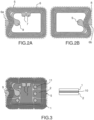
- FIG 1 represents a top view of an electrically conductive support or grid 1 designed to support contact pads on a first face 1a, such as ISO contacts 2, allowing dialogue between a chip and an external reader (not shown for reasons of simplification), the ISO contacts being connected via connection wells, 3, to the chip.
- the electrically conductive support can be of the rigid support type such as a lead frame known by the English expression “lead frame”.
- the metal of the grid is for example a copper alloy.
- Grid 1 can also be made of aluminum, having better resistance to corrosion and good compatibility with wire connection methods used to electrically connect connection pads with ISO contacts.
- the contact face 1a of the grid (external face) making contact with the claws of a card reader can be easily metallized with an essentially chemical metallization process of the “electroless” type.
- FIG 2A represents a low-cost flexible plastic support type substrate 6 comprising on a first face 6a an antenna 5 (electrically conductive zone).
- the low cost carrier can be made of polyethylene terephthalate or PET, or polyvinyl chloride or PVC.
- the antenna 5 in this example has several turns of conductive material produced by etching or by an additive process (process where the surface of the desired pattern is activated to allow the growth of the conductor in a second step or the direct transfer of the conductor, by screen printing or transfer, for example).
- the first face 6a comprising the antenna 5 comprises two connection pads 7 which will be used to connect a chip 12 to provide a contactless function. The coupling between the electronic module and an antenna buried in the card will be done in this case by inductive coupling ( figure 5B ).
- FIG 2B represents a second antenna 8 deposited on the face 6b opposite the first face 6a of the substrate 6.
- the second antenna 8 is itself composed of several turns in this example.
- the two antennas 5, 8 double-sided antenna
- the two faces of the substrate are electrically connected by crimping 9 between jaws with force and ultrasound, known by the English expression “crimp”.
- the technology for making antennas can be the large-width engraving (a few tens of cm to several meters) of a two-layer aluminum complex on a PET dielectric.
- the two conductive layers will then be interconnected by "crimp".
- antennas It is possible to use copper or silver ink as conductive materials.
- the realization of the antennas will be done, for example, by additive growth of the conductive material according to the model (pattern) chosen or any other available technology.
- a layer of adhesive 10 is deposited on the low-cost substrate in order to allow it to be fixed on the grid.
- the assembly formed by the “adhesive-coated” support is then perforated with several orifices 11 or solder wells which will be used to connect the chip to the ISO pads of the gate, providing a contact function.
- the perforation step can be carried out before or after the deposition of the adhesive layer.
- the adhesive layer When the adhesive layer is deposited after perforation of the substrate, the adhesive layer will be pre-perforated.
- the position of the orifices is chosen according to the position of the contacts arranged on the external face of the grid.
- the number of orifices 11 is five for the contact function and the number of connection pads (without contact) 7 is two for the contactless function.
- the number of connection pads is chosen according to the application.
- the "adhesive" and perforated support is then glued to the hidden face 1b of the grid, the face which does not include the finish for the ISO connection.
- the adhesive layer 10 optionally multi-layered, with a resistant core, makes it possible in particular to electrically insulate the metal (ISO layer) from the antenna in the case of a double-sided antenna.
- the etching varnish may have been kept at least for this face in order to ensure its electrical insulation.
- the holes 11 reveal the wiring areas to form solder wells for the electrical connection of the chip 12.
- FIG 4 illustrates an example of several positions of the grid on a support in continuous format of the S35 type, Super 35mm format, known from skilled in the art, on which we will come to transfer a flexible film with its conductors, pierced and inexpensive according to the method described above.
- the next step, figure 5A consists in bonding an integrated circuit or chip 12 on the flexible substrate or at the level of the flexible substrate according to principles known to those skilled in the art.
- the chip 12 could be positioned at the level of an opening 15 (shown in dotted lines in figure 5B ) in the plastic support in order to gain thickness.
- the chip 12 is then connected to the connection pads 7 corresponding to the ends of the antenna in order to ensure the function without contact and via the solder wells 11 with the contact pads 12p of the chip in order to ensure the function with contact.
- An encapsulation 13 and protection resin is deposited, in order to encompass the chip and the connections.
- FIG. 5B shows in section the positioning of an electronic module manufactured by the method of the invention above a cavity of a card 21 comprising an antenna 22 (electric circuit) placed on a support 23 in order to provide a contactless function.
- the geometry and the dimensions of the cavity 24 are chosen for example according to the dimension of the electronic module.
- the support of the electronic module has a certain thickness, for example 350-400 ⁇ m, allowing the presence of two electrically conductive zones 31 (metallic material) replacing the antenna 5 in the form of turns of the electronic module.
- the coupling between the electronic module and the antenna buried in a card is then done by capacitive coupling.
- the contacts in the example given verify ISO standards, but could also be other contacts suitable for other applications.
- the antenna is replaced by two connection pads adapted to be connected to the antenna located in a card body.
- Different technologies can be used, for example, conventional technologies with anisotropic conductive embedding adhesive film or ACF, or with conductive bump or bump, or even by using a conductive glue, or a solder, between the metal surfaces 31 and the terminals of the core antenna in the card body.
- the steps described are carried out for the manufacture of modules for dual or hybrid cards comprising a chip and used for banking transactions.
- the method according to the invention and the module obtained can also be used in the field of identity, for passports for example, or in any other field using such portable objects.
- the electronic module obtained by the invention has a low manufacturing cost.
- the product can be flexibly adapted to be compatible with all known dual interface board manufacturing technologies.
Description
- L'invention concerne un procédé de fabrication d'un module électronique pour un objet portatif comportant une fonction avec contact et/ou une fonction sans contact.
- Elle est notamment utilisée pour la fabrication de modules électroniques destinés à des cartes possédant une fonction avec contact et/ou sans contact, ces cartes pouvant être des cartes duals, hybrides. Les cartes obtenues peuvent être utilisées dans le domaine de l'identité, de la santé, du transport, etc.
- Un module électronique désigne en général une puce de circuit intégré fixée sur la face cachée (face opposée à la face du module en contact avec un lecteur) d'un boîtier de connexion au moyen d'un adhésif.
- Les modules électroniques sont en général réalisés sur des circuits imprimés flexibles avec une ou deux couches en cuivre gravé et métallisé. Les plots de la puce du circuit intégré sont électriquement connectés aux plaques de contact du boîtier de connexion au moyen de fils conducteurs. Pour pouvoir relier électriquement le module électronique à un autre circuit électrique noyé dans un corps de carte, le module électronique comprend en outre une antenne ou une paire de plaques de contact internes à la puce, disposées sur la face cachée du boîtier de connexion. L'antenne est électriquement liée à la puce via des plots et au moyen de fils conducteurs (technique connue sous le terme anglo-saxon « wire bonding »). ou par une technique de connexion directe utilisant des bossages conducteurs ou « bump » (technique connue sous le terme anglo-saxon « flip chip »).
- Ce type de technologie pour fabriquer un micromodule présente l'inconvénient d'être onéreux.
- Le document
EP2825001 divulgue une technique pour fabriquer un module électronique afin d'assurer une rigidité suffisante à tous les endroits du module qui présentent une faiblesse de tenue mécanique. - L'invention a notamment pour objectif de diminuer le coût de fabrication d'un module électronique tout en assurant les fonctions avec contact et/ou sans contact pour une utilisation donnée. A cet effet, on utilise un substrat souple faible coût que l'on va solidariser à un support électriquement conducteur pour constituer un boîtier de connexion d'un module électronique pour une carte comprenant une fonction contact et/ou une fonction sans contact.
- L'invention concerne un procédé de fabrication d'un ou plusieurs modules électroniques caractérisé en ce qu'il comporte au moins les étapes suivantes :
- Utiliser :
- Un substrat souple comportant plusieurs orifices traversant, et sur une première face au moins une zone électriquement conductrice, aux extrémités de laquelle se trouvent une ou plusieurs plages de connexion, et une deuxième face, et
- Un support électriquement conducteur comportant sur une première face une ou plusieurs zones de connexion, et une deuxième face,
- Assembler la deuxième face dudit substrat souple à ladite deuxième face dudit support électriquement conducteur au moyen d'une couche adhésive, Positionner un circuit intégré sur ou au niveau de la première face dudit substrat,
- Connecter un ou plusieurs contacts dudit circuit intégré à la ou aux zones de connexion via lesdits orifices de connexion, et aux plages de connexion, Déposer une couche de protection au niveau du circuit intégré.
- On assemble le substrat souple au support électriquement conducteur avant de perforer l'ensemble formé par le substrat et la couche adhésive.
- Selon un mode de réalisation, la zone électriquement conductrice est constituée de plusieurs spires formant une antenne. Les spires peuvent être en aluminium, constituées de cuivre ou encore d'une matière électriquement conductrice imprimée.
- La zone électriquement conductrice est formée, par exemple, d'au moins deux zones de matériau conducteur disposées autour du circuit intégré.
- Le support utilisé est par exemple un substrat en polyéthylène téréphtalate (PET) ou en Polychlorure de vinyle (PVC).
- L'invention concerne aussi un module électronique selon la revendication 9.
- Le substrat est, par exemple, réalisé en polyéthylène téréphtalate PET ou en Polychlorure de vinyle PVC.
- Selon un mode de réalisation, la zone électriquement conductrice est une antenne formée par au moins une spire déposée sur au moins une face du substrat.
- La zone électriquement conductrice peut être formée d'au moins deux zones de matériau conducteur disposées autour du circuit intégré.
- L'invention concerne aussi un objet portatif tel qu'une carte comprenant un module électronique selon l'invention, le module étant disposé dans une cavité de la carte, et une antenne déposée dans le corps de la carte.
- D'autres caractéristiques et avantages de la présente invention apparaîtront mieux à la lecture de la description d'exemples de réalisation, donnés à titre illustratif et nullement limitatif, annexée des figures qui représentent :
-
Figure 1 , une vue de dessus d'une grille supportant les contacts « physiques » avec un lecteur de carte externe, -
Figure 2A et 2B , une vue de dessus et de dessous du substrat flexible comprenant un circuit électrique sur chaque face, -
Figure 3 , une vue de dessus du substrat percé de plusieurs orifices permettant la connexion, -
Figure 4 , une vue d'ensemble de plusieurs positions de la grille sur un support au format continu de type S35 avant le report du film souple percé tel que décrit dans lafigure 3 , -
Figure 5A , une vue de dessus d'un module formé après découpe dans le format décrit par lafigure 4 et connexion d'un circuit intégré,figure 5B , une vue en coupe du module en position par rapport à une cavité d'une carte, et -
Figure 6 , une variante de réalisation d'un module comprenant deux plaques métalliques. - De façon à bien faire comprendre l'objet de l'invention, la description qui suit est donnée à titre d'exemple non limitatif pour fabriquer un module électronique destiné à être utilisé dans une carte comportant au moins une fonction de transaction (paiement ou autre) avec contact et/ou sans contact.
- La
figure 1 représente une vue de dessus d'un support électriquement conducteur ou grille 1 conçu pour supporter des plages de contact sur une première face 1a, tels que des contacts ISO 2, permettant le dialogue entre une puce et un lecteur externe (non représenté pour des raisons de simplification), les contacts ISO étant connectés via des puits de connexion, 3, à la puce. Le support électriquement conducteur peut être de type support rigide tel qu'une grille de connexion connue sous l'expression anglo-saxonne « lead frame ». - Le métal de la grille est par exemple un alliage cuivreux. La grille 1 peut aussi être en aluminium, présentant une meilleure résistance à la corrosion et une bonne compatibilité avec des procédés de connexion filaire utilisés pour connecter électriquement des plots de connexion avec les contacts ISO. La face contact 1a de la grille (face externe) faisant contact avec les griffes d'un lecteur de carte peut être facilement métallisée avec un procédé de métallisation essentiellement chimique de type « electroless ».
- La
figure 2A représente un substrat de type support en plastique souple faible coût 6 comportant sur une première face 6a une antenne 5 (zone électriquement conductrice). Le support faible coût peut être réalisé en polyéthylène téréphtalate ou PET, ou en Polychlorure de vinyle ou PVC. L'antenne 5 dans cet exemple présente plusieurs spires en matériau conducteur réalisées par gravure ou par un procédé additif (procédé où la surface du motif voulu est activée pour permettre la croissance du conducteur dans un second temps ou le report direct du conducteur, par sérigraphie ou transfert, par exemple). La première face 6a comprenant l'antenne 5 comporte deux plages de connexion 7 qui serviront à la connexion d'une puce 12 pour assurer une fonction sans contact. Le couplage entre le module électronique et une antenne enfouie dans la carte se fera dans ce cas par couplage inductif (figure 5B ). - La
figure 2B représente une deuxième antenne 8 déposée sur la face 6b opposée à la première face 6a du substrat 6. La deuxième antenne 8 est elle-même composée de plusieurs spires dans cet exemple. Les deux antennes 5, 8 (antenne double face) peuvent présenter des caractéristiques techniques identiques ou différentes selon les applications envisagées. Les deux faces du substrat sont connectées électriquement par sertissage 9 entre des mors avec force et ultrasons, connue sous l'expression anglo-saxonne « crimp ». - La technologie pour la réalisation des antennes peut être la gravure en grande laize (quelques dizaines de cm à plusieurs mètres) d'un complexe à deux couches d'aluminium sur un diélectrique PET. Les deux couches conductrices seront ensuite interconnectées par « crimp ».
- Il est possible d'utiliser comme matériaux conducteurs du cuivre ou de l'encre argent. La réalisation des antennes se fera, par exemple, par croissance additive du matériau conducteur selon le modèle (pattern) choisi ou toute autre technologie disponible.
- Une couche d'adhésif 10 est déposée sur le substrat et faible coût afin de permettre de le fixer sur la grille.
- On perfore ensuite l'ensemble formé par le support « adhésivé » de plusieurs orifices 11 ou puits de soudure qui vont être utilisés pour connecter la puce aux plots ISO de la grille, assurant une fonction avec contact. L'étape de perforation peut être réalisée avant ou après le dépôt de la couche adhésive. Lorsque la couche adhésive est déposée après perforation du substrat, la couche adhésive sera pré-perforée. La position des orifices est choisie en fonction de la position des contacts disposés sur la face externe de la grille.
- Dans l'exemple donné (
figure 3 ), le nombre d'orifices 11 est de cinq pour la fonction avec contact et le nombre des plages de connexion (sans contact) 7 est de deux pour la fonction sans contact. Le nombre de plages de connexion est choisi en fonction de l'application. - Le support « adhésivé » et perforé est ensuite collé sur la face cachée 1b de la grille, la face qui ne comporte pas la finition pour la connexion ISO. La couche adhésive 10, éventuellement multicouche, avec une âme résistante, permet notamment d'isoler électriquement le métal (couche ISO) de l'antenne dans le cas d'une antenne double face. Le vernis de gravure peut avoir été conservé au moins pour cette face afin d'assurer son isolement électrique. Les orifices 11 laissent apparaître les zones de câblage pour constituer des puits de soudure pour la connexion électrique de la puce 12.
- La
figure 4 illustre, un exemple de plusieurs positions de la grille sur un support au format continu de type S35, format Super 35mm, connu de l'homme du métier, sur laquelle on va venir reporter un film souple avec ses conducteurs, percé et peu coûteux selon le procédé exposé ci-avant. - L'étape suivante,
figure 5A , consiste à coller un circuit intégré ou puce 12 sur le substrat souple ou au niveau du substrat souple selon des principes connus de l'homme du métier. Par exemple, la puce 12 pourrait être positionnée au niveau d'une ouverture 15 (représentée en pointillés enfigure 5B ) dans le support plastique afin de gagner en épaisseur. La puce 12 est ensuite connectée aux plages de connexion 7 correspondant aux extrémités de l'antenne afin d'assurer la fonction sans contact et via les puits de soudure 11 avec les plots de contact 12p de la puce afin d'assurer la fonction avec contact. Une résine d'encapsulation 13 et de protection est déposée, afin d'englober la puce et les connexions. - L'exécution des étapes décrites ci-dessus permet d'obtenir un module électronique dual interface avec antenne qui est compatible avec un procédé d'encartage.
- La
figure 5B représente en coupe le positionnement d'un module électronique fabriqué par le procédé de l'invention au-dessus d'une cavité d'une carte 21 comprenant une antenne 22 (circuit électrique) disposée sur un support 23 afin d'assurer une fonction sans contact. La géométrie et les dimensions de la cavité 24 sont choisies par exemple en fonction de la dimension du module électronique. - Selon une variante de réalisation,
figure 6 , le support du module électronique présente une certaine épaisseur, par exemple 350-400µm, permettant la présence de deux zones électriquement conductrices 31 (matériau métallique) remplaçant l'antenne 5 en forme de spires du module électronique. Le couplage entre le module électronique et l'antenne enfouie dans une carte se fait alors par couplage capacitif. - Les contacts dans l'exemple donné vérifient les normes ISO, mais pourraient aussi être d'autres contacts adaptés à d'autres applications.
- Selon une variante de réalisation, l'antenne est remplacée par deux plots de connexion adaptés à être connectés à l'antenne située dans un corps de carte. Différentes technologies peuvent être utilisées, par exemple, des technologies classiques avec Film d'adhésif d'encartage conducteur anisotropique ou ACF, ou avec bossage conducteur ou Bump, ou encore en utilisant une colle conductrice, ou une soudure, entre les surfaces métalliques 31 et les bornes de l'antenne à coeur dans le corps de carte.
- Les étapes décrites sont exécutées pour la fabrication de modules pour cartes dual ou hybrides comprenant une puce et utilisées pour des transactions bancaires. Le procédé selon l'invention et le module obtenu peuvent aussi être utilisés dans le domaine de l'identité, pour des passeports par exemple, ou dans tout autre domaine utilisant de telles objets portatifs.
- Le module électronique obtenu par l'invention présente un faible coût de fabrication.
- Le produit peut être décliné avec flexibilité pour être compatible avec toutes les technologies de fabrications de cartes dual interfaces connues.
Claims (13)
- - Procédé de fabrication d'un ou plusieurs modules électroniques (20) caractérisé en ce qu'il comporte au moins les étapes suivantes :Utiliser :Un substrat souple (6) comportant plusieurs orifices de connexion (11) traversant et sur une première face (6a) au moins une zone (5) électriquement conductrice, aux extrémités de laquelle se trouvent une ou plusieurs plages de connexion (7), et une deuxième face (6b), etUn support électriquement conducteur (1) comportant sur une première face (1a), une ou plusieurs zones de connexion (3), et une deuxième face (1b),Assembler la deuxième face (6b) dudit substrat souple (6) à ladite deuxième face (1b) dudit support électriquement conducteur (1) au moyen d'une couche adhésive,Positionner un circuit intégré (12) sur ou au niveau de la première face (6a) dudit substrat (6),Connecter un ou plusieurs contacts (12p) dudit circuit intégré (12) à la ou aux zones de connexion (3) via lesdits orifices de connexion (11), et aux plages de connexion (7),Déposer une couche de protection (13) au niveau du circuit intégré.
- - Procédé de fabrication selon la revendication 1 caractérisé en ce que l'on assemble le substrat souple au support électriquement conducteur avant de perforer l'ensemble formé par le substrat et la couche adhésive.
- - Procédé selon l'une des revendications 1 ou 2 caractérisé en ce que la zone électriquement conductrice (5) est constituée de plusieurs spires formant une antenne.
- - Procédé selon la revendication 3 caractérisé en ce que les spires sont constituées d'aluminium.
- - Procédé selon la revendication 3 caractérisé en ce que les spires sont constituées de cuivre.
- - Procédé selon la revendication 3 caractérisé en ce que les spires sont constituées de matière électriquement conductrice imprimée.
- - Procédé selon l'une des revendications 1 ou 2 caractérisé en ce que la zone électriquement conductrice (5) est formée d'au moins deux zones de matériau conducteur (31) disposées autour du circuit intégré.
- - Procédé selon l'une des revendications précédentes caractérisé en ce que l'on utilise un substrat en polyéthylène téréphtalate (PET) ou en Polychlorure de vinyle (PVC).
- - Module électronique caractérisé en ce qu'il comporte au moins les éléments suivants :• Un substrat souple (6) comprenant sur une première face (6a) au moins une zone électriquement conductrice (5), aux extrémités de laquelle se trouvent une ou plusieurs plages de connexion (7), et une deuxième face (6b), plusieurs orifices (11) de connexion traversant,• Un support électriquement conducteur (1) comportant sur une première face (1a) une ou plusieurs zones de connexion (3), et une deuxième face (1b),• Ledit substrat souple (6) est fixé via ladite deuxième face (6b) à ladite deuxième face (1b) dudit support électriquement conducteur (1) au moyen d'une couche adhésive,• Un circuit intégré (12) disposé sur ou au niveau de la première face (6a) du substrat (6), ledit circuit intégré (12) étant relié via un ou plusieurs plots (12p) à la au moins une zone électriquement conductrice (5) via lesdits orifices de connexion (11),• Une couche de protection (13) au niveau au moins du circuit intégré.
- - Module électronique selon la revendication 9 caractérisé en ce que le substrat est en polyéthylène téréphtalate (PET), ou en Polychlorure de vinyle (PVC).
- - Module électronique selon l'une des revendications 9 ou 10 caractérisé en ce que la zone électriquement conductrice (5) est une antenne formée par au moins une spire déposée sur au moins une face du substrat.
- - Module électronique selon l'une des revendications 9 ou 10 caractérisé en ce que la zone électriquement conductrice (5) est formée d'au moins deux zones de matériau conducteur (31) disposées autour du circuit intégré.
- - Carte comprenant un module électronique selon l'une des revendications 9 à 12 disposé dans une cavité (13) de la carte et une antenne déposée dans le corps de la carte.
Applications Claiming Priority (2)
| Application Number | Priority Date | Filing Date | Title |
|---|---|---|---|
| FR1858425A FR3086098B1 (fr) | 2018-09-18 | 2018-09-18 | Procede de fabrication d'un module electronique pour objet portatif |
| PCT/EP2019/074069 WO2020058036A1 (fr) | 2018-09-18 | 2019-09-10 | Procede de fabrication d'un module electronique pour objet portatif |
Publications (2)
| Publication Number | Publication Date |
|---|---|
| EP3853773A1 EP3853773A1 (fr) | 2021-07-28 |
| EP3853773B1 true EP3853773B1 (fr) | 2023-07-26 |
Family
ID=65201497
Family Applications (1)
| Application Number | Title | Priority Date | Filing Date |
|---|---|---|---|
| EP19763008.0A Active EP3853773B1 (fr) | 2018-09-18 | 2019-09-10 | Procede de fabrication d'un module electronique pour objet portatif |
Country Status (5)
| Country | Link |
|---|---|
| EP (1) | EP3853773B1 (fr) |
| KR (1) | KR20210060476A (fr) |
| CN (1) | CN112703510B (fr) |
| FR (1) | FR3086098B1 (fr) |
| WO (1) | WO2020058036A1 (fr) |
Family Cites Families (14)
| Publication number | Priority date | Publication date | Assignee | Title |
|---|---|---|---|---|
| FR2880160B1 (fr) * | 2004-12-28 | 2007-03-30 | K Sa As | Module electronique double face pour carte a puce hybride |
| JP4952266B2 (ja) * | 2007-01-18 | 2012-06-13 | 大日本印刷株式会社 | デュアルインターフェースicカードとその製造方法、接触・非接触兼用icモジュール |
| CN101971194A (zh) * | 2007-12-19 | 2011-02-09 | 谢玉莲 | 非接触式和双界面嵌体及其生产方法 |
| CN101350073B (zh) * | 2008-08-20 | 2010-06-23 | 北京握奇数据系统有限公司 | 双界面智能卡的生产方法、双界面智能卡及其天线层 |
| CN102663480B (zh) * | 2012-03-24 | 2016-05-25 | 上海仪电智能电子有限公司 | 一种双界面智能卡 |
| FR2992761B1 (fr) * | 2012-07-02 | 2015-05-29 | Inside Secure | Procede de fabrication d'un microcircuit sans contact |
| FR2996944B1 (fr) * | 2012-10-15 | 2018-05-04 | Smart Packaging Solutions Sps | Module electronique simplifie pour carte a puce a double interface de communication |
| SG11201510464UA (en) * | 2013-07-10 | 2016-02-26 | Gemalto Sa | Dielectric filmless electronic module and method for manufacturing same |
| EP2825001A1 (fr) * | 2013-07-10 | 2015-01-14 | Gemalto SA | Module électronique à film dielectrique adhésif et son procédé de fabrication |
| EP2871595A1 (fr) * | 2013-11-12 | 2015-05-13 | Gemalto SA | Carte à puce comprenant un module électronique électriquement connecté à un circuit électrique |
| WO2015157659A1 (fr) * | 2014-04-10 | 2015-10-15 | American Banknote Corporation | Module à circuit intégré pour une carte intelligente à deux interfaces |
| FR3021145B1 (fr) * | 2014-05-14 | 2018-08-31 | Linxens Holding | Procede de fabrication d'un circuit pour module de carte a puce et circuit pour module de carte a puce |
| EP3159831B1 (fr) * | 2015-10-21 | 2018-10-03 | Nxp B.V. | Carte à circuit intégré double interface |
| FR3047101B1 (fr) * | 2016-01-26 | 2022-04-01 | Linxens Holding | Procede de fabrication d’un module de carte a puce et d’une carte a puce |
-
2018
- 2018-09-18 FR FR1858425A patent/FR3086098B1/fr active Active
-
2019
- 2019-09-10 CN CN201980060756.6A patent/CN112703510B/zh active Active
- 2019-09-10 EP EP19763008.0A patent/EP3853773B1/fr active Active
- 2019-09-10 KR KR1020217008059A patent/KR20210060476A/ko not_active Application Discontinuation
- 2019-09-10 WO PCT/EP2019/074069 patent/WO2020058036A1/fr unknown
Also Published As
| Publication number | Publication date |
|---|---|
| FR3086098A1 (fr) | 2020-03-20 |
| WO2020058036A1 (fr) | 2020-03-26 |
| FR3086098B1 (fr) | 2020-12-04 |
| KR20210060476A (ko) | 2021-05-26 |
| CN112703510A (zh) | 2021-04-23 |
| CN112703510B (zh) | 2024-02-20 |
| EP3853773A1 (fr) | 2021-07-28 |
Similar Documents
| Publication | Publication Date | Title |
|---|---|---|
| EP0671705B1 (fr) | Procédé de fabrication d'une carte hybride | |
| EP3567527B1 (fr) | Procédé de fabrication d'un circuit pour module de carte à puce et circuit pour module de carte à puce | |
| EP3574451B1 (fr) | Dispositif rfid et procédé de fabrication | |
| EP3092604B1 (fr) | Module électronique, son procédé de fabrication, et dispositif électronique comprenant un tel module | |
| WO2014191428A1 (fr) | Procédé de fabrication d'un circuit imprimé, circuit imprimé obtenu par ce procédé et module électronique comportant un tel circuit imprimé | |
| WO2020212660A1 (fr) | Module de capteur biométrique pour carte à puce et procédé de fabrication d'un tel module | |
| FR3003723A1 (fr) | Procede de fabrication d'un circuit imprime flexible, circuit imprime flexible obtenu par ce procede et module de carte a puce comportant un tel circuit imprime flexible | |
| JP7474251B2 (ja) | チップカード用電子モジュール | |
| EP3853773B1 (fr) | Procede de fabrication d'un module electronique pour objet portatif | |
| EP2915104B1 (fr) | Procédé de fabrication d'un connecteur pour module de carte à puce, connecteur de carte à puce obtenu par ce procédé et module de carte à puce comportant un tel connecteur | |
| EP3853775B1 (fr) | Procede de fabrication d'un module a carte et le module obtenu | |
| EP2866173A1 (fr) | Procédé de réalisation d'un circuit électrique et circuit électrique réalisé par ce procédé | |
| FR2810768A1 (fr) | Procede de fabrication de cartes a puce hybrides et cartes a puce obtenues par ledit procede | |
| FR3083892A1 (fr) | Carte a puce a double interface de communication et son procede de fabrication | |
| EP1623367A1 (fr) | Procede de fabrication d'un inlet prelamine | |
| FR2795202A1 (fr) | Carte et procede de fabrication de cartes ayant une interface de communication a contact et sans contact | |
| EP3020068B1 (fr) | Module electronique et son procede de fabrication | |
| FR3005391A1 (fr) | Procede de fabrication d'un circuit flexible pour module de carte a puce, circuit flexible de carte a puce otenu par ce procede et module de carte a puce comportant un tel circuit flexible | |
| WO2017153353A1 (fr) | Procede de fabrication de module a puce de circuit integre et dispositif comprenant un tel module |
Legal Events
| Date | Code | Title | Description |
|---|---|---|---|
| STAA | Information on the status of an ep patent application or granted ep patent |
Free format text: STATUS: UNKNOWN |
|
| STAA | Information on the status of an ep patent application or granted ep patent |
Free format text: STATUS: THE INTERNATIONAL PUBLICATION HAS BEEN MADE |
|
| PUAI | Public reference made under article 153(3) epc to a published international application that has entered the european phase |
Free format text: ORIGINAL CODE: 0009012 |
|
| STAA | Information on the status of an ep patent application or granted ep patent |
Free format text: STATUS: REQUEST FOR EXAMINATION WAS MADE |
|
| 17P | Request for examination filed |
Effective date: 20210225 |
|
| AK | Designated contracting states |
Kind code of ref document: A1 Designated state(s): AL AT BE BG CH CY CZ DE DK EE ES FI FR GB GR HR HU IE IS IT LI LT LU LV MC MK MT NL NO PL PT RO RS SE SI SK SM TR |
|
| DAV | Request for validation of the european patent (deleted) | ||
| DAX | Request for extension of the european patent (deleted) | ||
| GRAP | Despatch of communication of intention to grant a patent |
Free format text: ORIGINAL CODE: EPIDOSNIGR1 |
|
| STAA | Information on the status of an ep patent application or granted ep patent |
Free format text: STATUS: GRANT OF PATENT IS INTENDED |
|
| INTG | Intention to grant announced |
Effective date: 20230214 |
|
| GRAS | Grant fee paid |
Free format text: ORIGINAL CODE: EPIDOSNIGR3 |
|
| GRAA | (expected) grant |
Free format text: ORIGINAL CODE: 0009210 |
|
| STAA | Information on the status of an ep patent application or granted ep patent |
Free format text: STATUS: THE PATENT HAS BEEN GRANTED |
|
| AK | Designated contracting states |
Kind code of ref document: B1 Designated state(s): AL AT BE BG CH CY CZ DE DK EE ES FI FR GB GR HR HU IE IS IT LI LT LU LV MC MK MT NL NO PL PT RO RS SE SI SK SM TR |
|
| REG | Reference to a national code |
Ref country code: CH Ref legal event code: EP |
|
| REG | Reference to a national code |
Ref country code: DE Ref legal event code: R096 Ref document number: 602019033602 Country of ref document: DE |
|
| REG | Reference to a national code |
Ref country code: IE Ref legal event code: FG4D Free format text: LANGUAGE OF EP DOCUMENT: FRENCH |
|
| REG | Reference to a national code |
Ref country code: LT Ref legal event code: MG9D |
|
| REG | Reference to a national code |
Ref country code: NL Ref legal event code: MP Effective date: 20230726 |
|
| REG | Reference to a national code |
Ref country code: AT Ref legal event code: MK05 Ref document number: 1592789 Country of ref document: AT Kind code of ref document: T Effective date: 20230726 |
|
| PG25 | Lapsed in a contracting state [announced via postgrant information from national office to epo] |
Ref country code: NL Free format text: LAPSE BECAUSE OF FAILURE TO SUBMIT A TRANSLATION OF THE DESCRIPTION OR TO PAY THE FEE WITHIN THE PRESCRIBED TIME-LIMIT Effective date: 20230726 |
|
| PG25 | Lapsed in a contracting state [announced via postgrant information from national office to epo] |
Ref country code: GR Free format text: LAPSE BECAUSE OF FAILURE TO SUBMIT A TRANSLATION OF THE DESCRIPTION OR TO PAY THE FEE WITHIN THE PRESCRIBED TIME-LIMIT Effective date: 20231027 |
|
| PGFP | Annual fee paid to national office [announced via postgrant information from national office to epo] |
Ref country code: GB Payment date: 20231121 Year of fee payment: 5 |
|
| PG25 | Lapsed in a contracting state [announced via postgrant information from national office to epo] |
Ref country code: IS Free format text: LAPSE BECAUSE OF FAILURE TO SUBMIT A TRANSLATION OF THE DESCRIPTION OR TO PAY THE FEE WITHIN THE PRESCRIBED TIME-LIMIT Effective date: 20231126 |
|
| PG25 | Lapsed in a contracting state [announced via postgrant information from national office to epo] |
Ref country code: SE Free format text: LAPSE BECAUSE OF FAILURE TO SUBMIT A TRANSLATION OF THE DESCRIPTION OR TO PAY THE FEE WITHIN THE PRESCRIBED TIME-LIMIT Effective date: 20230726 Ref country code: RS Free format text: LAPSE BECAUSE OF FAILURE TO SUBMIT A TRANSLATION OF THE DESCRIPTION OR TO PAY THE FEE WITHIN THE PRESCRIBED TIME-LIMIT Effective date: 20230726 Ref country code: PT Free format text: LAPSE BECAUSE OF FAILURE TO SUBMIT A TRANSLATION OF THE DESCRIPTION OR TO PAY THE FEE WITHIN THE PRESCRIBED TIME-LIMIT Effective date: 20231127 Ref country code: NO Free format text: LAPSE BECAUSE OF FAILURE TO SUBMIT A TRANSLATION OF THE DESCRIPTION OR TO PAY THE FEE WITHIN THE PRESCRIBED TIME-LIMIT Effective date: 20231026 Ref country code: LV Free format text: LAPSE BECAUSE OF FAILURE TO SUBMIT A TRANSLATION OF THE DESCRIPTION OR TO PAY THE FEE WITHIN THE PRESCRIBED TIME-LIMIT Effective date: 20230726 Ref country code: LT Free format text: LAPSE BECAUSE OF FAILURE TO SUBMIT A TRANSLATION OF THE DESCRIPTION OR TO PAY THE FEE WITHIN THE PRESCRIBED TIME-LIMIT Effective date: 20230726 Ref country code: IS Free format text: LAPSE BECAUSE OF FAILURE TO SUBMIT A TRANSLATION OF THE DESCRIPTION OR TO PAY THE FEE WITHIN THE PRESCRIBED TIME-LIMIT Effective date: 20231126 Ref country code: HR Free format text: LAPSE BECAUSE OF FAILURE TO SUBMIT A TRANSLATION OF THE DESCRIPTION OR TO PAY THE FEE WITHIN THE PRESCRIBED TIME-LIMIT Effective date: 20230726 Ref country code: GR Free format text: LAPSE BECAUSE OF FAILURE TO SUBMIT A TRANSLATION OF THE DESCRIPTION OR TO PAY THE FEE WITHIN THE PRESCRIBED TIME-LIMIT Effective date: 20231027 Ref country code: FI Free format text: LAPSE BECAUSE OF FAILURE TO SUBMIT A TRANSLATION OF THE DESCRIPTION OR TO PAY THE FEE WITHIN THE PRESCRIBED TIME-LIMIT Effective date: 20230726 Ref country code: AT Free format text: LAPSE BECAUSE OF FAILURE TO SUBMIT A TRANSLATION OF THE DESCRIPTION OR TO PAY THE FEE WITHIN THE PRESCRIBED TIME-LIMIT Effective date: 20230726 |
|
| PGFP | Annual fee paid to national office [announced via postgrant information from national office to epo] |
Ref country code: FR Payment date: 20231121 Year of fee payment: 5 Ref country code: DE Payment date: 20231120 Year of fee payment: 5 |
|
| PG25 | Lapsed in a contracting state [announced via postgrant information from national office to epo] |
Ref country code: PL Free format text: LAPSE BECAUSE OF FAILURE TO SUBMIT A TRANSLATION OF THE DESCRIPTION OR TO PAY THE FEE WITHIN THE PRESCRIBED TIME-LIMIT Effective date: 20230726 |
|
| PG25 | Lapsed in a contracting state [announced via postgrant information from national office to epo] |
Ref country code: ES Free format text: LAPSE BECAUSE OF FAILURE TO SUBMIT A TRANSLATION OF THE DESCRIPTION OR TO PAY THE FEE WITHIN THE PRESCRIBED TIME-LIMIT Effective date: 20230726 |
|
| PG25 | Lapsed in a contracting state [announced via postgrant information from national office to epo] |
Ref country code: SM Free format text: LAPSE BECAUSE OF FAILURE TO SUBMIT A TRANSLATION OF THE DESCRIPTION OR TO PAY THE FEE WITHIN THE PRESCRIBED TIME-LIMIT Effective date: 20230726 Ref country code: RO Free format text: LAPSE BECAUSE OF FAILURE TO SUBMIT A TRANSLATION OF THE DESCRIPTION OR TO PAY THE FEE WITHIN THE PRESCRIBED TIME-LIMIT Effective date: 20230726 Ref country code: ES Free format text: LAPSE BECAUSE OF FAILURE TO SUBMIT A TRANSLATION OF THE DESCRIPTION OR TO PAY THE FEE WITHIN THE PRESCRIBED TIME-LIMIT Effective date: 20230726 Ref country code: EE Free format text: LAPSE BECAUSE OF FAILURE TO SUBMIT A TRANSLATION OF THE DESCRIPTION OR TO PAY THE FEE WITHIN THE PRESCRIBED TIME-LIMIT Effective date: 20230726 Ref country code: DK Free format text: LAPSE BECAUSE OF FAILURE TO SUBMIT A TRANSLATION OF THE DESCRIPTION OR TO PAY THE FEE WITHIN THE PRESCRIBED TIME-LIMIT Effective date: 20230726 Ref country code: CZ Free format text: LAPSE BECAUSE OF FAILURE TO SUBMIT A TRANSLATION OF THE DESCRIPTION OR TO PAY THE FEE WITHIN THE PRESCRIBED TIME-LIMIT Effective date: 20230726 Ref country code: SK Free format text: LAPSE BECAUSE OF FAILURE TO SUBMIT A TRANSLATION OF THE DESCRIPTION OR TO PAY THE FEE WITHIN THE PRESCRIBED TIME-LIMIT Effective date: 20230726 |
|
| REG | Reference to a national code |
Ref country code: CH Ref legal event code: PL |