EP3840128A1 - Bodenplatte, elektronisches bauteil und verfahren - Google Patents
Bodenplatte, elektronisches bauteil und verfahren Download PDFInfo
- Publication number
- EP3840128A1 EP3840128A1 EP20215925.7A EP20215925A EP3840128A1 EP 3840128 A1 EP3840128 A1 EP 3840128A1 EP 20215925 A EP20215925 A EP 20215925A EP 3840128 A1 EP3840128 A1 EP 3840128A1
- Authority
- EP
- European Patent Office
- Prior art keywords
- circuit board
- base plate
- section
- contact
- force
- Prior art date
- Legal status (The legal status is an assumption and is not a legal conclusion. Google has not performed a legal analysis and makes no representation as to the accuracy of the status listed.)
- Pending
Links
- 238000000034 method Methods 0.000 title claims description 23
- 230000000149 penetrating effect Effects 0.000 claims abstract description 3
- 238000005476 soldering Methods 0.000 claims abstract description 3
- 238000003825 pressing Methods 0.000 claims description 42
- RYGMFSIKBFXOCR-UHFFFAOYSA-N Copper Chemical compound [Cu] RYGMFSIKBFXOCR-UHFFFAOYSA-N 0.000 claims description 8
- 229910052802 copper Inorganic materials 0.000 claims description 8
- 239000010949 copper Substances 0.000 claims description 8
- 239000002184 metal Substances 0.000 claims description 6
- 229910052751 metal Inorganic materials 0.000 claims description 6
- 238000004519 manufacturing process Methods 0.000 description 14
- 239000004020 conductor Substances 0.000 description 7
- 238000013459 approach Methods 0.000 description 4
- 239000000463 material Substances 0.000 description 4
- 238000010521 absorption reaction Methods 0.000 description 3
- 239000012777 electrically insulating material Substances 0.000 description 3
- PXHVJJICTQNCMI-UHFFFAOYSA-N Nickel Chemical compound [Ni] PXHVJJICTQNCMI-UHFFFAOYSA-N 0.000 description 2
- 239000011248 coating agent Substances 0.000 description 2
- 238000000576 coating method Methods 0.000 description 2
- 238000006073 displacement reaction Methods 0.000 description 2
- BQCADISMDOOEFD-UHFFFAOYSA-N Silver Chemical compound [Ag] BQCADISMDOOEFD-UHFFFAOYSA-N 0.000 description 1
- 229910000831 Steel Inorganic materials 0.000 description 1
- 230000000712 assembly Effects 0.000 description 1
- 238000000429 assembly Methods 0.000 description 1
- 230000005540 biological transmission Effects 0.000 description 1
- 230000015572 biosynthetic process Effects 0.000 description 1
- 230000000694 effects Effects 0.000 description 1
- PCHJSUWPFVWCPO-UHFFFAOYSA-N gold Chemical compound [Au] PCHJSUWPFVWCPO-UHFFFAOYSA-N 0.000 description 1
- 229910052737 gold Inorganic materials 0.000 description 1
- 239000010931 gold Substances 0.000 description 1
- 230000002427 irreversible effect Effects 0.000 description 1
- 239000002655 kraft paper Substances 0.000 description 1
- 230000013011 mating Effects 0.000 description 1
- 229910052759 nickel Inorganic materials 0.000 description 1
- 230000036316 preload Effects 0.000 description 1
- 230000002028 premature Effects 0.000 description 1
- 230000000284 resting effect Effects 0.000 description 1
- 229910052709 silver Inorganic materials 0.000 description 1
- 239000004332 silver Substances 0.000 description 1
- 125000006850 spacer group Chemical group 0.000 description 1
- 239000010959 steel Substances 0.000 description 1
- 238000012876 topography Methods 0.000 description 1
- 238000003466 welding Methods 0.000 description 1
Images




Classifications
-
- H—ELECTRICITY
- H01—ELECTRIC ELEMENTS
- H01R—ELECTRICALLY-CONDUCTIVE CONNECTIONS; STRUCTURAL ASSOCIATIONS OF A PLURALITY OF MUTUALLY-INSULATED ELECTRICAL CONNECTING ELEMENTS; COUPLING DEVICES; CURRENT COLLECTORS
- H01R12/00—Structural associations of a plurality of mutually-insulated electrical connecting elements, specially adapted for printed circuits, e.g. printed circuit boards [PCB], flat or ribbon cables, or like generally planar structures, e.g. terminal strips, terminal blocks; Coupling devices specially adapted for printed circuits, flat or ribbon cables, or like generally planar structures; Terminals specially adapted for contact with, or insertion into, printed circuits, flat or ribbon cables, or like generally planar structures
- H01R12/50—Fixed connections
- H01R12/51—Fixed connections for rigid printed circuits or like structures
- H01R12/55—Fixed connections for rigid printed circuits or like structures characterised by the terminals
- H01R12/58—Fixed connections for rigid printed circuits or like structures characterised by the terminals terminals for insertion into holes
- H01R12/585—Terminals having a press fit or a compliant portion and a shank passing through a hole in the printed circuit board
-
- H—ELECTRICITY
- H01—ELECTRIC ELEMENTS
- H01H—ELECTRIC SWITCHES; RELAYS; SELECTORS; EMERGENCY PROTECTIVE DEVICES
- H01H50/00—Details of electromagnetic relays
- H01H50/02—Bases; Casings; Covers
- H01H50/021—Bases; Casings; Covers structurally combining a relay and an electronic component, e.g. varistor, RC circuit
-
- H—ELECTRICITY
- H01—ELECTRIC ELEMENTS
- H01H—ELECTRIC SWITCHES; RELAYS; SELECTORS; EMERGENCY PROTECTIVE DEVICES
- H01H45/00—Details of relays
- H01H45/02—Bases; Casings; Covers
-
- H—ELECTRICITY
- H01—ELECTRIC ELEMENTS
- H01H—ELECTRIC SWITCHES; RELAYS; SELECTORS; EMERGENCY PROTECTIVE DEVICES
- H01H50/00—Details of electromagnetic relays
- H01H50/02—Bases; Casings; Covers
- H01H50/04—Mounting complete relay or separate parts of relay on a base or inside a case
- H01H50/047—Details concerning mounting a relays
- H01H50/048—Plug-in mounting or sockets
-
- H—ELECTRICITY
- H01—ELECTRIC ELEMENTS
- H01H—ELECTRIC SWITCHES; RELAYS; SELECTORS; EMERGENCY PROTECTIVE DEVICES
- H01H50/00—Details of electromagnetic relays
- H01H50/14—Terminal arrangements
-
- H—ELECTRICITY
- H01—ELECTRIC ELEMENTS
- H01R—ELECTRICALLY-CONDUCTIVE CONNECTIONS; STRUCTURAL ASSOCIATIONS OF A PLURALITY OF MUTUALLY-INSULATED ELECTRICAL CONNECTING ELEMENTS; COUPLING DEVICES; CURRENT COLLECTORS
- H01R43/00—Apparatus or processes specially adapted for manufacturing, assembling, maintaining, or repairing of line connectors or current collectors or for joining electric conductors
- H01R43/20—Apparatus or processes specially adapted for manufacturing, assembling, maintaining, or repairing of line connectors or current collectors or for joining electric conductors for assembling or disassembling contact members with insulating base, case or sleeve
- H01R43/205—Apparatus or processes specially adapted for manufacturing, assembling, maintaining, or repairing of line connectors or current collectors or for joining electric conductors for assembling or disassembling contact members with insulating base, case or sleeve with a panel or printed circuit board
-
- H—ELECTRICITY
- H01—ELECTRIC ELEMENTS
- H01R—ELECTRICALLY-CONDUCTIVE CONNECTIONS; STRUCTURAL ASSOCIATIONS OF A PLURALITY OF MUTUALLY-INSULATED ELECTRICAL CONNECTING ELEMENTS; COUPLING DEVICES; CURRENT COLLECTORS
- H01R12/00—Structural associations of a plurality of mutually-insulated electrical connecting elements, specially adapted for printed circuits, e.g. printed circuit boards [PCB], flat or ribbon cables, or like generally planar structures, e.g. terminal strips, terminal blocks; Coupling devices specially adapted for printed circuits, flat or ribbon cables, or like generally planar structures; Terminals specially adapted for contact with, or insertion into, printed circuits, flat or ribbon cables, or like generally planar structures
- H01R12/70—Coupling devices
- H01R12/71—Coupling devices for rigid printing circuits or like structures
- H01R12/72—Coupling devices for rigid printing circuits or like structures coupling with the edge of the rigid printed circuits or like structures
- H01R12/722—Coupling devices for rigid printing circuits or like structures coupling with the edge of the rigid printed circuits or like structures coupling devices mounted on the edge of the printed circuits
- H01R12/724—Coupling devices for rigid printing circuits or like structures coupling with the edge of the rigid printed circuits or like structures coupling devices mounted on the edge of the printed circuits containing contact members forming a right angle
Definitions
- the invention relates to a base plate for an electronic component, in particular an electronic relay.
- the invention also relates to a relay with a base plate and a method for the electrical and mechanical connection of a base plate to a circuit board of a relay.
- a standardized system is usually used here, which defines the interface to the mating connector in the form of contact arrangement and contact geometry in accordance with the relevant ISO standards 7588 or 8092.
- Electromechanical relays are manufactured in millions of pieces and in some cases also fully automatically. This is usually not the case with electronic relays. This is due, on the one hand, to the number of different variants and, on the other, to manufacturing challenges. In the case of electromechanical relays, the relay coil body is often already connected to some of the contacts.
- the electromechanical relays are basically very similar in terms of structure and number of pins, so that they can be automated comparatively better.
- individual contacts are mounted on the circuit board and then soldered. These contacts are then fixed and aligned by a plastic plate. In some cases, the contacts also have a type of latching so that they can be fixed in the base plate. In this way, mechanical forces that arise from the assembly of the assembly or from vibration during operation can be absorbed.
- the printed circuit board is mounted directly on the base plate in a spatially parallel manner.
- standard contacts are soldered onto the circuit board and then mounted in the base plate. The unbundling then takes place on the circuit board. Smaller circuits can then also be implemented directly here. Due to the fact that the contacts are soldered on the circuit board, the available area is comparatively small depending on the number of contacts. Also, wired components such as relays can only be equipped with increased effort.
- both approaches have the disadvantage that the contacts or the base plate must be aligned during assembly. If the contacts are not installed at right angles or correctly, mechanical forces are transferred to the circuit board and can damage the soldered joints, which can lead to premature failure of the module. Both systems therefore do not enable economically viable automated production with smaller quantities or only with greater effort. Also due to the fact that more and more functions have to be integrated into these comparatively small electronic assemblies and the space on the printed circuit board is very limited, new manufacturing techniques have to be developed.
- the invention is therefore based on the object of specifying an electronic component, in particular an electronic relay, which can be produced in an automated process and whose production effort is reduced.
- the invention proposes a base plate for an electronic component, in particular an electronic relay, having a plate-shaped base body, in particular made of plastic, and at least one electrical contact, the electrical contact completely penetrating the base body, the electrical contact at one end forms an electrical connector of the electronic component, in particular of the relay, the electrical contact having an electrically conductive connection section at the other end, which can be connected to a circuit board without soldering, in particular pressed into the circuit board, to form a permanent electrical connection.
- the solution is based on the idea of replacing the mechanically fragile soldered connections with a different type of electrical and mechanical connection.
- the invention makes use of press-fit technology for the first time in the field of electronic components, in particular relays.
- press-in technology there are different options for creating a press-in zone on the contact.
- the press-in zone can preferably be designed as a force-absorbing section on the outer edge or in the surface of the contacts.
- the contacts are preferably designed with an angular, in particular rectangular, square cross-section. In principle, contacts with a round cross-section are also possible.
- the solder-free connection according to the invention between the base plate and printed circuit board creates the prerequisite for electronic relays to be connected to the base plate according to the invention in an automated process can be produced.
- the manufacturing cost of the relay is reduced in an advantageous manner by completely dispensing with soldered connections between the circuit board and the contacts of the base plate.
- Press-in technology also has the advantage that the contact resistance of a press-in connection is significantly lower than that of a soldered joint. When using power electronics, this technology reduces the heat generated by the assembly and thus increases the efficiency of the assembly.
- the connecting section can be single-ended, double-ended or multi-ended. Each end can be separately connected to the circuit board, in particular it can be pressed into the circuit board. Depending on the desired functionality of the relay, different contacts can have connecting sections configured differently with regard to the number of their ends.
- the individual ends are designed in the form of a pin.
- the various pins of a connecting section preferably extend at a distance from one another and parallel to one another in the same direction.
- the pins can have an angular and / or round cross-section.
- the connection points of the circuit board that correspond to the pins can also be designed to be correspondingly round and / or angular, depending on the cross-sectional geometry of the respective pin.
- At least one of the contacts is angled.
- the section of the contact that forms the connection of the relay extends in a different direction than the connection section used for connection to the circuit board. Both sections preferably run at right angles to one another.
- the individual sections of the contact are preferably bent at the desired angle to one another. Due to the press-fit technique, the base plate is automatically aligned, preferably at right angles, to the circuit board when it is connected to the circuit board. The components on the circuit board do not have to be heated again. This reduces the stress on the components.
- the connecting section extends, at least in some areas, essentially parallel to the flat side of the base body facing it.
- the connecting section can be introduced into a corresponding opening in the circuit board by linear movement of the base plate and / or the contact. Complex movements in more than one direction are avoided in this way, which is advantageous with regard to the automation of the manufacturing process of the relay.
- the electrical contact and / or the base body has a force-absorbing section which extends at an angle, in particular at a right angle, to the connection section.
- a force-absorbing section which extends at an angle, in particular at a right angle, to the connection section.
- the introduction of force cannot take place via one of the ends of the contacts, as is usually the case. This is especially the case when the contacts are angled in order to achieve an angled, preferably right-angled, alignment between the base plate and the circuit board in the relay. If, in this case, the forces required for pressing are nevertheless to be transmitted to the circuit board via the base plate or via the contacts, it is preferred to define force-absorbing sections.
- the contact Due to the geometric configuration of the contacts, however, the force cannot be applied linearly to the contact at one end. Instead, the contact has specially designed force-absorbing sections via which the press-in force can act on the contact.
- provision can be made for the base plate to be moved linearly (horizontally or vertically) in the direction of the printed circuit board.
- the circuit board can also be moved linearly in the direction of the base plate for the purpose of connection.
- a force absorption section can be provided by an edge or a flat side of the contact and / or of the base body.
- a force absorption section itself can be designed as an edge section, side section and / or as a recess, in particular as a notch.
- a notch can be linear or punctiform.
- a linear notch offers the advantage of a homogeneous introduction of force over a larger area. By means of a punctiform notch, comparatively high forces can be transmitted selectively to the contact and / or the base body.
- the contact In the case of the angled, in particular right-angled, configuration of the contact, it has two legs resting against the angle.
- the end of the first leg has the section which forms the connection of the relay.
- the second leg provides the connection section at the end.
- the force-absorbing section and the connecting section are provided by the second leg of the contact.
- the force-absorbing section directly adjoins the connecting section in the direction of the angle of the contact.
- the force-absorbing section preferably extends at an angle, in particular at a right angle, with respect to the connecting section.
- the force-absorbing section is preferably angled in the opposite direction to the first angle.
- the force-absorbing section thus preferably extends parallel to the first leg. you further preferably extend in the same direction. the force-absorbing section preferably extends beyond the first leg in the direction of extent.
- the press-in can take place exclusively or additionally via the contacts.
- at least one stamp is preferably provided, which acts on the at least one contact for the purpose of pressing in.
- a force transmitter is preferably provided in the form of a separate component, in particular a mask, which is pushed over the contacts.
- the force transmitter is preferably geometrically formed on the at least one contact, preferably on a plurality of contacts.
- the force-absorbing section is designed to run between the base body and the connecting section.
- the force-absorbing section is preferably formed in contact. This improves the introduction of force into the contact. In particular, in the case of an angled configuration of the contact, undesired opposing leverage effects are avoided.
- the contacts can basically have any cross-sectional geometry.
- the contacts can in particular be angular or round in cross section.
- the electrical contact is designed as a plate-shaped rod.
- the rod has a rectangular cross section at least in some areas.
- the stand has a rectangular outer contour, at least in some areas.
- the force-absorbing section is preferably formed by at least one of the narrow edges of the rod.
- the force-absorbing section is from a flat section of the rod.
- the contact preferably has a right-angled cross-section. This improves the transmission of force to the contact.
- the force-absorbing section preferably runs between the connecting section and the end of the contact which forms the relay connection.
- the contact is preferably formed from an electrically conductive material, preferably a metal, in particular copper.
- the contact can be formed from any material, in particular a plastic, and coated with an electrically conductive material, preferably a metal, in particular copper.
- the basic body the base plate is preferably made of an electrically insulating material, preferably a plastic.
- the contacts are preferably guided in the base body. This is used for the precise alignment to the printed circuit board. They are more preferably anchored in the base body. This has the advantage that the contacts cannot be pressed out of the base body while they are being pressed in.
- the invention also relates to an electronic component, in particular a relay, preferably an electronic relay, having a base plate according to the invention and a circuit board, the base plate and circuit board being arranged to one another in such a way that the flat side of the base body of the base plate and the flat side of the The base body of the printed circuit board extend essentially at right angles to one another, characterized in that the printed circuit board has at least one contact point into which the connecting section of the at least one contact of the base plate is pressed for electrical and mechanical connection.
- the use of the press-fit technology according to the invention advantageously results in the electrical connection between the circuit board and contact of the base plate and the mechanical fastening and alignment of the base plate on the circuit board at the same time. This is made possible by the use of the base plate according to the invention.
- the component according to the invention in particular a relay, can be produced in an automated process by virtue of the design according to the invention. In this way, manufacturing effort and costs can be reduced in an advantageous manner.
- the contact point is designed as a bore and / or as a slot.
- the slot is preferably designed as a color.
- the bore and / or the slot are preferably coated on the inside with a conductive material, in particular copper.
- a conductive material in particular copper.
- the contact point has an inner circumference which is smaller than the outer circumference of the connecting section of the contact. During the press-in process, the connecting section of the contact is pressed into the contact point with material displacement and is fixed in place there.
- the conductive material of the contact point is displaced.
- the displacement can be an irreversible material removal.
- a desired cold welding can occur between the connection section and the contact point. This further improves the stability of the connection.
- the connecting section and / or the contact point is at least partially compressible at right angles to the press-in direction. This can be done in particular by applying a spring preload. In this case, the fixation can be realized without removing material.
- the contact point is designed in the form of a plated-through hole.
- a “through-hole connection” denotes an electrical connection between different conductor levels of a circuit board by means of a bore.
- the method according to the invention completely dispenses with the formation of soldered connections when forming the electrical connection between the contacts of the base plate and the circuit board. Instead, it uses only the pressing of the contacts of the base plate into the contact points of the circuit board. As a result, the method can be designed to be completely automated. Manufacturing effort and This considerably reduces manufacturing costs for the relay according to the invention. Particularly in view of the shortage of skilled workers and the wage costs in Germany, the relay according to the invention can be manufactured by means of the method according to the invention in a significantly more cost-effective manner, in higher quality and in larger numbers.
- the pressing device has a pressing ram which is brought into engagement with the force-absorbing section during the pressing process.
- the engagement can preferably be positive.
- the ram has a receptacle designed to correspond to the force absorbing section, in particular a receiving slot.
- the recording therefore acts as a positioning aid.
- the frictional engagement prevents the ram from slipping during the pressing process; especially in an automated process.
- the ram can be brought into engagement directly with the force-absorbing section. Alternatively, the ram can be indirectly brought into engagement with the force receiving section with the interposition of an aforementioned force transmitter.
- the positioning device and / or pressing device are designed as robots, the positioning and the pressing being carried out by means of the robot.
- the positioning device and the pressing device can be designed as separate robots. Alternatively, both devices can be designed as a robot. This automates the process to a greater extent. Production effort and production costs for the relay according to the invention are further reduced as a result.
- the invention makes use of press-fit technology for the first time in the field of manufacturing electronic relays.
- Press-fit technology per se may be known from the state of the art, but precisely not with reference to electronic relays, which differ from the usual areas of application of press-fit technology due to a large number of inherent technical features. It was only through the invention that press-fit technology was made usable for the production of electronic relays.
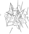
- Figure 1 shows a floor panel 1 according to a first embodiment of the invention.
- the base plate 1 has a base body 2 and nine contacts 3.
- the bottom plate 1 is shown with released contacts 3 which are inserted at different depths into receiving slots 4 formed in the bottom plate 1.
- the base body 1 has a separate slot 4 for each contact 3.
- the base body 1 has a substantially rectangular circumference with rounded corners. It is formed from an electrically insulating material in the form of plastic and also serves to relieve strain on the contacts 3.
- the contacts 3 are designed as angled metal plates. They are preferably made of copper-plated and tin-plated steel.
- Each contact 3 is designed at one end as an electrical connection plug 5, 6, 7 for a relay according to the invention.
- the connection plugs 5 are designed as 2.8 mm connections.
- the connection plugs 6 are designed as 6.3 mm connections.
- the connection plugs 7 are designed as a 9.5 mm connection.
- each contact 3 has a connecting section 8.
- the connecting sections 8 run to the respective connector 5, 6, 7 of the contact 3 at a right angle.
- At least one force-absorbing section 9 is formed between the end 5, 6, 7 of the contact 3, designed as a connector, and the connecting section 8.
- at least one press die is brought into engagement with at least one force-absorbing section 9.
- the ram then transmits a force perpendicular to the respective force receiving section 9 and in the direction of extension of the pins 10.
- each of the connecting sections 8 has at least one pin 10 for connection to a contact point on the printed circuit board.
- the number of pins is determined by the current carrying capacity that the contacts are supposed to provide. In the present case, 5 of the contacts 3 have two pins 10 and 4 of the contacts 3 have a pin 10.
- the connecting sections 8 have a web 11 and / or at least one contact edge 12 for the electrical connection to the printed circuit board. The webs 11 and contact edges 12 also serve to fix the contact 3 on the base body 2.
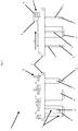
- Figure 2 shows the base plate 1 according to the invention in two different side views.
- the contacts 3 are shown in the fixed state. In this fixed state, the contacts 3 are pressed into the circuit board.
- the press rams are brought into engagement with the force absorbing sections 9 and a pressing force is transmitted in the pressing direction A perpendicular to the force absorbing sections 9.
- connection plug 5 (2.8 mm), connection plug 6 (6.3 mm) and connection plug 7 (9.5 mm) with different dimensions.
- the base plate 1 in the present case has two 9.5 mm connection plugs, three 6.3 mm connection plugs and four 2.3 mm connection plugs.
- Figure 3 shows the base plate 1 according to the invention in a perspective view.
- the contacts 3 are in the fixed state on the base body.
- the force absorbing sections 9 each extend at right angles to the respective connecting section 8.
- the force absorbing sections 9 are each formed by the narrow edges of the plate-shaped contacts 3.
- the Figures 4 to 7 show a floor panel 1 according to a second embodiment of the invention.
- the base plate 1 has a base body 2 and nine contacts 3.
- the basic structure, however, is the same.
- the features of the various embodiments can therefore be transferred to one another and / or combined with one another without any problems.
- FIG. 4 Shown in Figure 4 is the base plate 1 with released contacts 3, which in the present case are inserted at different depths into receiving slots 7 formed in the base body 2 for the purpose of illustration.
- Each contact 3 is designed at one end as an electrical connection plug 5, 6 for a relay according to the invention.
- the connection plugs 5 are designed as 2.8 mm connections.
- the connection plugs 6 are designed as 6.3 mm connections. in the In contrast to the embodiment according to Figure 1 no connector 7 with a 9.5 mm connection is provided.
- Figure 5 shows the base plate 1 according to Figure 4 in two different side views.
- the contacts 3 are shown in the fixed state. In this fixed state, the contacts 3 are pressed into the circuit board.
- the press rams are brought into engagement with the force absorbing sections 9 and a pressing force is transmitted in the pressing direction A perpendicular to the force absorbing sections 9.
- connection plug 5 (2.8 mm) and connection plug 6 (6.3 mm) designed with different dimensions.
- the contacts 3 are also shown in the fixed state, in which the contacts 3 are immovably connected to the base body 2.
- the base body 2 has a separate slot 4 for each contact 3.
- the base body 2 has an essentially rectangular circumference with rounded corners. It is made of an electrically insulating material in the form of plastic.
- each of the connecting sections 8 has at least one pin 10 for the respective connection to a contact point on the printed circuit board.
- Figure 7 shows the base plate 1 in a view from below with a view of the ends of the contacts 3 designed as connection plugs 5, 6.
- the base plate in the present case has five 6.3 mm connection plugs and four 2.3 mm connection plugs.
- Figures 8 and 9 shows a press-fit system according to the invention for performing the press-fit process according to the invention.
- Figure 8 time the components of the system in an exploded view.
- Figure 9 shows the system in the pressed-in state.
- the main body 2 and the contacts 3, which together form the base plate 1, can be seen.
- a printed circuit board 13 is also shown.
- the printed circuit board 13 has a multiplicity of contact points in the form of holes 14.
- the holes 14 can at least partially be designed as bores.
- the pins 10 are pressed into the holes 14.
- There each hole 14 receives a pin 10 in the pressed-in state.
- the holes 14 are positioned in the printed circuit board 13 in a manner corresponding to the arrangement of the pins 10 in the fixed state.
- the holes 14 have a conductive material such as copper, nickel, silver, gold or the like on the inside.
- the holes 14 are coated on the inside with copper. This serves, on the one hand, for the electrical connection of circuit board 13 and base plate 1.Furthermore, while the pins 10 are pressed in, part of the copper coating is removed by the pressing force acting on the contacts 3, with a mechanical clamping connection, in particular a force-fit connection, between hole 14 and pin 10 is created.
- a first pressing device 15 can also be seen.
- the first pressing device 15 has a device 16 for receiving the printed circuit board 13.
- the device 16 is formed from two holders 17 arranged parallel to one another. Each holder 17 has a fastening web 18 on both ends.
- the fastening webs 18 of a holder 17 have an arcuate contour on their mutually facing side 19. The contour is convex.
- a total of four circular arc-shaped concave recesses 21 are formed in the circumferential edge 20 of the circuit board 13.
- the printed circuit board 13 can be inserted into the device 16 in such a way that in each case a fastening web 18 engages with its convex side 19 in a concave recess 21.
- a second pressing device 22 is shown.
- the pressing device 22 is brought into engagement with the base plate 1 in order to press the contacts 3 into the circuit board 13.
- the pressing device 22 has a continuous pressing section 23.
- the pressing section 23 is matched to the number, arrangement and shape of the contacts 3.
- the pressing section 23 thereby has sub-sections 24 which are brought into engagement with the force-absorbing sections 9 during the pressing-in, in order to transmit a pressing force from the pressing device 22 to the base plate 1.
- each subsection 56 forms a press die.
- pressing force is transmitted directly to the base body 2 by means of a further sub-section of the pressing section 23.
- the sub-section is brought into engagement in sections with one of the two edges 25, 26 of the base body 2, which edges are arranged one above the other in a step-like manner.
- the pressing device 22 is designed as a one-piece molded part. In principle, it can be made of plastic and / or metal. In the present case it is made of metal.
- the pressing device 22 ensures that the pressing force is distributed particularly evenly to the base plate 1 and in particular to the contacts 3. Damage to the base plate 1, the contacts 3 and the circuit board 13 is therefore prevented.
- the pressing device 22 also has two guide elements 27, 28 on the holder side.
- the guide elements 27, 28 are designed as rectangular projections in the pressing device 22. As intended, they serve as a centering aid and / or as an end stop during press-fit. For this purpose, they interact with one of the holders 17 in such a way that a guide element 27, 28 is guided along a fastening web 18.
- the guide elements 27, 28 are in direct contact with a plate section 29 running at right angles to the fastening webs 18. In this state, they act as spacers and mark the end point of the pressing path. The guide elements 27, 28 thus ensure that the printed circuit board 13 is not damaged.
- the plate section 29 can be designed in such a way that corresponding bores are formed below the position of the pins 10 in the pressed-in state, so that the pins 10 can penetrate there during and after the press-in process or have space and the force around the bore is absorbed can and thus the circuit board 13 is not damaged.
- the base plate 1 and the printed circuit board 13 are connected to one another in such a way that their mutually facing surfaces extend at an angle of 90 ° to one another.
- the two embodiments serve only to illustrate the invention. This expressly does not exclude other embodiments.
- the invention is not restricted to the use of standard dimensions for connector plugs. Rather, instead of the standardized designs with cross-sectional lengths of 2.8 mm, 6.3 mm or 9.5 mm, dimensions that differ from this are also possible such as 2mm, 6mm, or 10mm. In the context of the invention, connector plugs with cross-sectional lengths between 1 mm and 12 mm are therefore possible in principle.
Landscapes
- Physics & Mathematics (AREA)
- Electromagnetism (AREA)
- Engineering & Computer Science (AREA)
- Manufacturing & Machinery (AREA)
- Coupling Device And Connection With Printed Circuit (AREA)
Abstract
Description
- Die Erfindung betrifft eine Bodenplatte für ein elektronisches Bauteil, insbesondere ein elektronisches Relais. Ferner betrifft die Erfindung ein Relais mit einer Bodenplatte und ein Verfahren zur elektrischen und mechanischen Verbindung einer Bodenplatte mit einer Leiterplatte eines Relais.
- Elektronische Schaltungen werden häufig in Relaisgehäusen untergebracht. Hier setzt man in der Regel auf ein genormtes System auf, welches die Schnittstelle zum Gegenstecker in Form von Kontaktanordnung und Kontaktgeometrie gemäß der einschlägigen ISO-Normen 7588 oder 8092 definiert.
- Elektromechanische Relais werden in Millionen Stückzahlen und teilweise auch vollautomatisch gefertigt. Bei elektronischen Relais ist das in der Regel nicht der Fall. Dies ist zum einen der Anzahl verschiedener Varianten und zum anderen fertigungstechnischen Herausforderungen geschuldet. Bei den elektromechanischen Relais ist der Relais-Spulenkörper oft auch schon mit einem Teil der Kontakte verbunden. Die elektromechanischen Relais sind vom Aufbau, Anzahl der Pins, grundsätzlich sehr ähnlich, so dass sich diese vergleichsweise besser automatisieren lassen.
- Zur Fertigung elektronischer Bausätze gibt es verschiedene Ansätze.
- Gemäß einem ersten Ansatz werden einzelne Kontakte auf die Leiterplatte montiert und anschließend verlötet. Diese Kontakte werden dann durch eine Kunststoffplatte fixiert und ausgerichtet. Teilweise haben die Kontakte dann auch eine Art Verrastung um in der Bodenplatte fixiert werden zu können. Dadurch können mechanische Kräfte die durch die Montage der Baugruppe oder im Betrieb durch Vibration entstehen aufgenommen werden.
- Gemäß einem zweiten Ansatz wird die Leiterplatte direkt auf der Bodenplatte räumlich parallel ausgerichtet montiert. Bei diesem Konzept werden Standardkontakte auf die Leiterkarte aufgelötet und dann in die Bodenplatte montiert. Die Entflechtung erfolgt dann auf der Leiterplatte. Kleinere Schaltungen können dann auch direkt hier realisiert werden. Aufgrund dessen, dass die Kontakte auf der Leiterkarte verlötet werden, ist die verfügbare Fläche je nach Kontaktanzahl vergleichsweise gering. Auch lassen sich bedrahtete Bauteile wie Relais nur mit erhöhtem Aufwand bestücken.
- Beide Ansätze haben jedoch den Nachteil, dass die Ausrichtung der Kontakte oder der Bodenplatte bei der Montage erfolgen muss. Wenn die Kontakte nicht rechtwinklig oder vorschriftsmäßig montiert sind, werden mechanische Kräfte auf die Leiterkarte übertragen und können die Lötstellen beschädigen, was zu einem verfrühten Ausfall der Baugruppe führen kann. Beide Systeme ermöglichen damit keine wirtschaftlich sinnvolle automatisierte Produktion bei geringeren Stückzahlen oder nur mit höheren Aufwand. Auch aufgrund dessen, dass immer mehr Funktionsumfang in diese vergleichsweise kleinen elektronischen Baugruppen integriert werden muss und der Platz der Leiterkarte sehr begrenzt ist, müssen neue Fertigungstechniken entwickelt werden.
- Der Erfindung liegt damit die Aufgabe zu Grunde, ein elektronisches Bauteil, insbesondere ein elektronisches Relais, anzugeben, welches in einem automatisierten Verfahren herstellbar und dessen Fertigungsaufwand verringert ist.
- Zur Lösung dieser Aufgabe schlägt die Erfindung eine Bodenplatte für ein elektronisches Bauteil, insbesondere ein elektronisches Relais, vor, aufweisend einen plattenförmigen Grundkörper, insbesondere aus Kunststoff, und wenigstens einem elektrischen Kontakt, wobei der elektrische Kontakt den Grundkörper vollständig durchgreift, wobei der elektrische Kontakt einendseitig einen elektrischen Anschlussstecker des elektronischen Bauteils, insbesondere des Relais, bildet, wobei der elektrische Kontakt andernendseitig einen elektrisch leitfähigen Verbindungsabschnitt aufweist, welcher mit einer Leiterplatte zur Ausbildung einer dauerhaften elektrischen Verbindung lötfrei verbindbar, insbesondere in die Leiterplatte einpressbar, ist.
- Der Lösung liegt der Gedanke zugrunde, die mechanisch fragilen Lötverbindungen durch eine andere Art der elektrischen und der mechanischen Verbindung zu ersetzen. Die Erfindung macht sich im Bereich der elektronischen Bauteile, insbesondere der Relais, erstmalig die Einpresstechnik zunutze. Bei der Einpresstechnik gibt es unterschiedliche Möglichkeiten am Kontakt eine Einpresszone auszuführen. Die Einpresszone kann bevorzugt als Kraftaufnahmeabschnitt an der Außenkante oder in der Fläche der Kontakte ausgeführt werden. Die Kontakte sind dabei vorzugsweise mit eckigem, insbesondere rechteckigem, quadratischen Querschnitt ausgebildet. Prinzipiell sind auch Kontakte mit rundem Querschnitt möglich. Durch die erfindungsgemäße lötfreie Verbindung zwischen Bodenplatte und Leiterplatte ist die Voraussetzung dafür geschaffen, dass elektronische Relais mit der erfindungsgemäßen Bodenplatte in einem automatisierten Verfahren hergestellt werden können. Darüber hinaus ist der Fertigungsaufwand des Relais durch den vollständigen Verzicht auf Lötverbindungen zwischen Leiterplatte und den Kontakten der Bodenplatte in vorteilhafter Weise verringert. Die Einpresstechnik bringt auch den Vorteil, dass der Übergangswiderstand einer Einpressverbindung wesentlich geringer als der einer Lötstelle ist. Bei Verwendung von Leistungselektronik reduziert diese Technologie die Wärmeentwicklung der Baugruppe und steigert somit die Effizienz der Baugruppe.
- Der Verbindungsabschnitt kann einendig, zweiendig oder mehrendig ausgebildet sein. Jedes Ende ist dabei mit der Leiterplatte gesondert verbindbar, insbesondere in die Leiterplatte einpressbar. Verschiedene Kontakte können je nach gewünschter Funktionalität des Relais hinsichtlich der Anzahl ihrer Enden unterschiedlich ausgestaltete Verbindungsabschnitte aufweisen. Die einzelnen Enden sind dabei in Form eines Pins ausgebildet. Vorzugsweise erstrecken sich die verschiedenen Pins eines Verbindungsabschnitts beabstandet und parallel zueinander in die gleiche Richtung. Die Pins können im Querschnitt eckig und/oder rund ausgebildet sein. Ebenso können die mit den Pins korrespondierenden Verbindungsstellen der Leiterplatte in Abhängigkeit der Querschnittsgeometrie des jeweiligen Pins ebenfalls korrespondierend rund und/oder eckig ausgebildet sein.
- Gemäß einem bevorzugten Merkmal der Erfindung ist wenigstens einer der Kontakte winklig ausgebildet. Der den Anschluss des Relais bildende Abschnitt des Kontakts erstreckt sich dabei in eine andere Richtung als der der Verbindung mit der Leiterplatte dienende Verbindungsabschnitt. Vorzugsweise verlaufen beide Abschnitte im rechten Winkel zueinander. Vorzugsweise sind die einzelnen Abschnitte des Kontakts zu diesem Zweck im gewünschten Winkel zueinander umgebogen. Durch die Einpresstechnik wird dabei die Bodenplatte bei der Verbindung mit der Leiterplatte automatisch, vorzugsweise rechtwinklig, zur Leiterplatte ausgerichtet. Die Bauteile auf der Leiterplatte müssen kein weiteres Mal erwärmt werden. Dies reduziert den Stress für die Bauteile.
- Gemäß einem bevorzugten Merkmal der Erfindung ist es vorgesehen, dass sich der Verbindungsabschnitt wenigstens bereichsweise im Wesentlichen parallel zu der ihm zugewandten flächigen Seite des Grundkörpers erstreckt. Hierdurch kann der Verbindungsabschnitt durch lineare Bewegung der Bodenplatte und/oder des Kontakts in eine korrespondierende Öffnung der Leiterplatte eingeführt werden. Komplexe Bewegungen in mehr als eine Richtung werden hierdurch vermieden, was hinsichtlich der Automatisierung des Herstellungsprozesses des Relais von Vorteil ist.
- Gemäß einem bevorzugten Merkmal der Erfindung ist vorgesehen, dass der elektrische Kontakt und/oder der Grundkörper einen Kraftaufnahmeabschnitt aufweist, welcher sich winklig, insbesondere rechtwinklig, zu dem Verbindungsabschnitt erstreckt. Im Gegensatz zu aus dem Stand der Technik bekannten Erzeugnissen, welche mittels Einpresstechnik hergestellt werden können, kann die Krafteinleitung nicht über eines der Enden der Kontakte erfolgen, wie dies üblicherweise der Fall ist. Dies ist im Besonderen dann der Fall, wenn die Kontakte winklig ausgebildet sind, um eine winklige, vorzugsweise rechtwinklige, Ausrichtung zwischen Bodenplatte und Leiterplatte im Relais zu realisieren. Sollen in diesem Fall die zur Einpressung notwendigen Kräfte gleichwohl über die Bodenplatte oder über die Kontakte auf die Leiterkarte übertragen werden, ist es bevorzugt, Kraftaufnahmeabschnitte zu definieren. Aufgrund der geometrischen Ausgestaltung der Kontakte kann jedoch nicht einendseitig auf den Kontakt linear die Kraft eingebracht werden. Stattdessen weist der Kontakt eigens dafür ausgebildete Kraftaufnahmeabschnitte auf, über welche die Einpresskraft auf den Kontakt wirken kann. Zusätzlich kann es vorgesehen sein, die Bodenplatte linear (horizontal oder vertikal) in Richtung der Leiterkarte zu bewegen. Alternativ kann auch die Leiterplatte linear in Richtung der Bodenplatte zum Zwecke der Verbindung bewegt werden. Ein Kraftaufnahmeabschnitt kann dabei von eine Kante oder eine flächige Seite des Kontakts und/oder des Grundkörpers bereitgestellt sein. Ein Kraftaufnahmeabschnitt selbst kann als Kantenabschnitt, Seitenabschnitt und/oder als Ausnehmung, insbesondere als Einkerbung, ausgebildet sein. Eine Einkerbung kann linienförmig oder punktförmig ausgebildet sein. Eine linienförmige Einkerbung bietet den Vorteil einer homogenen Krafteinleitung über einen größeren Bereich. Über eine punktförmige Einkerbung lassen sich vergleichsweise hohe Kräfte punktuell auf den Kontakt und/oder den Grundkörper übertragen.
- Im Falle der gewinkelten, insbesondere rechtwinkligen, Ausgestaltung des Kontakts weist dieser zwei an den Winkel anliegende Schenkel auf. Der erste Schenkel weist dabei endseitig den Abschnitt auf, der den Anschluss des Relais bildet. Der zweite Schenkel stellt demgegenüber endseitig den Verbindungsabschnitt bereit. Es ist bevorzugt, dass Kraftaufnahmeabschnitt und Verbindungsabschnitt von dem zweiten Schenkel des Kontakts bereitgestellt werden. Besonders bevorzugt schließt sich der Kraftaufnahmeabschnitt in Richtung auf den Winkel des Kontakts zu unmittelbar an den Verbindungsabschnitt an. Der Kraftaufnahmeabschnitt erstreckt sich gegenüber dem Verbindungsabschnitt vorzugsweise in einem Winkel, insbesondere in einem rechten Winkel. Vorzugsweise ist der Kraftaufnahmeabschnitt in entgegengesetzter Richtung zum ersten Winkel abgewinkelt. Der Kraftaufnahmeabschnitt erstreckt sich damit vorzugsweise parallel zum ersten Schenkel. Sie erstrecken sich weiter vorzugsweise in die gleiche Richtung. bevorzugt erstreckt sich der Kraftaufnahmeabschnitt in Erstreckungsrichtung über den ersten Schenkel hinaus.
- Die Einpressung kann ausschließlich oder zusätzlich über die Kontakte erfolgen. Hierzu sind vorzugsweise wenigstens ein Stempel vorgesehen, welcher auf den wenigstens einen Kontakt zum Zwecke des Einpressens einwirkt. Alternativ ist vorzugsweise ein Kraftüberträger in Form eines separaten Bauteils, insbesondere einer Maske, vorgesehen, welcher über die Kontakte geschoben wird, möglich. Der Kraftüberträger ist hierzu vorzugsweise an den wenigstens einen Kontakt, vorzugsweise an eine Mehrzahl von Kontakten, geometrisch angeformt.
- Gemäß einem bevorzugten Merkmal der Erfindung ist vorgesehen dass der Kraftaufnahmeabschnitt zwischen Grundkörper und Verbindungsabschnitt verlaufend ausgebildet ist. Vorzugsweise ist der Kraftaufnahmeabschnitt dabei im Kontakt ausgebildet. Hierdurch wird die Krafteinleitung in den Kontakt verbessert. Insbesondere werden im Falle einer winkligen Ausgestaltung des Kontakts unerwünschte gegengerichtete Hebeleffekte vermieden.
- Erfindungsgemäß können die Kontakte eine dem Grunde nach beliebige Querschnittsgeometrie aufweisen. Die Kontakte können im Querschnitt insbesondere eckig oder rund ausgebildet sein. Gemäß einem bevorzugten Merkmal der Erfindung ist vorgesehen, dass der elektrische Kontakt als plattenförmiger Stab ausgebildet ist. Der Stab weist wenigstens bereichsweise einen rechteckigen Querschnitt auf. Ferner weist der Stand wenigstens bereichsweise eine rechteckige Außenkontur auf. Der Kraftaufnahmeabschnitt ist dabei vorzugsweise von wenigstens einer der schmalen Kanten des Stabs gebildet sein. Gemäß einer alternativen bevorzugten Ausgestaltung ist der Kraftaufnahmeabschnitt von einem flächigen Abschnitt des Stabs Vorzugsweise weist der Kontakt einen rechtwinkligen Querschnitt auf. Hierdurch wird die Kraftübertragung auf den Kontakt verbessert. Der Kraftaufnahmeabschnitt verläuft vorzugsweise zwischen dem Verbindungsabschnitt und dem den Relaisanschluss bildenden Ende des Kontakts.
- Der Kontakt ist vorzugsweise aus einem elektrisch leitfähigen Material, vorzugsweise ein Metall, insbesondere Kupfer, gebildet. Alternativ Kann der Kontakt aus einem beliebigen Material, insbesondere einem Kunststoff gebildet und mit einem elektrisch leitfähigen Material, vorzugsweise ein Metall, insbesondere Kupfer, beschichtet sein. Der Grundkörper der Bodenplatte ist vorzugsweise aus einem elektrisch isolierenden Material, vorzugsweise einem Kunststoff, gebildet.
- Vorzugsweise sind die Kontakte in dem Grundkörper geführt. Dies dient der positionsgenauen Ausrichtung zur Leiterplatte. Weiter bevorzugt sind sie im Grundkörper verankert. Dies hat den Vorteil, dass die Kontakte während des Einpressens nicht aus dem Grundkörper herausgedrückt werden können.
- Die Erfindung betrifft ferner ein elektronisches Bauteil, insbesondere ein Relais, bevorzugt ein elektronisches Relais, aufweisend eine Bodenplatte gemäß der Erfindung und eine Leiterplatte, wobei Bodenplatte und Leiterplatte derart zueinander angeordnet sind, dass sich die flächige Seite des Grundkörpers der Bodenplatte und die flächige Seite des Grundkörpers der Leiterplatte im Wesentlichen im rechten Winkel zueinander erstrecken, dadurch gekennzeichnet, dass die Leiterplatte wenigstens eine Kontaktstelle aufweist, in welche der Verbindungsabschnitt des wenigstens einen Kontakts der Bodenplatte zur elektrischen und einer mechanischen Verbindung eingepresst ist.
- Durch den erfindungsgemäßen Einsatz der Einpresstechnik erfolgt in vorteilhafter Weise zeitgleich die elektrische Verbindung zwischen Leiterplatte und Kontakt der Bodenplatte sowie die mechanische Befestigung und Ausrichtung der Bodenplatte an der Leiterplatte. Ermöglicht wird dies durch die Verwendung der erfindungsgemäßen Bodenplatte. Das erfindungsgemäße Bauteil, insbesondere Relais, kann durch die erfindungsgemäße Ausbildung in einem automatisierten Verfahren hergestellt werden. Hierdurch lassen sich Fertigungsaufwand und -kosten in vorteilhafter Weise verringern.
- Gemäß einem bevorzugten Merkmal des Bauteils, insbesondere Relais, ist vorgesehen, dass die Kontaktstelle als Bohrung und/oder als Schlitz ausgebildet ist. Der Schlitz ist vorzugsweise als Färbung ausgebildet. Die Bohrung und/oder der Schlitz sind dabei vorzugsweise innenseitig mit einem leitfähigen Material, insbesondere Kupfer, beschichtet. Alternativ zu einer Beschichtung besteht die Möglichkeit, die Bohrung mit einer eine Aufnahme für den Verbindungsabschnitt des Kontakts bereitstellenden Hülse aus einem leitfähigen Material, insbesondere Kupfer, zu bestücken. Die Kontaktstelle weist dabei einen Innenumfang auf, der kleiner ist, als der Außenumfang des Verbindungsabschnitts des Kontakts. Bei dem Einpressvorgang wird der Verbindungsabschnitt des Kontakts unter Materialverdrängung in die Kontaktstelle eingepresst und dort ortsfest fixiert. Vorzugsweise wird das leitfähige Material der Kontaktstelle verdrängt. Die Verdrängung kann ein irreversibler Materialabtrag sein. In Abhängigkeit der anliegenden Presskraft kann es zwischen Verbindungsabschnitt und Kontaktstelle zu einer erwünschten Kaltverschweißung kommen. Hierdurch wird die Stabilität der Verbindung weiter verbessert. Alternativ ist der Verbindungsabschnitt und/oder die Kontaktstelle im rechten Winkel zur Einpressrichtung wenigstens teilweise kompressibel ausgebildet. Dies kann insbesondere durch Anlegung einer Federvorspannung erfolgen. In diesem Fall kann die Fixierung ohne Materialabtrag realisiert werden.
- Vorzugsweise kann vorgesehen sein, dass die Kontaktstelle in Form einer Durchkontaktierung ausgebildet ist. Eine "Durchkontaktierung" bezeichnet im Sinne der Erfindung eine elektrische Verbindung verschiedener Leiterebenen einer Leiterplatte mittels einer Bohrung.
- Die Erfindung betrifft ferner ein Verfahren zur elektrischen und mechanischen Verbindung einer Bodenplatte und einer Leiterplatte eines erfindungsgemäßen elektronischen Bauteils, insbesondere eines elektronischen Relais, bei dem
- mittels einer Positioniereinrichtung die Grundkörper der Bodenplatte und der Leiterplatte derart angeordnet werden, dass sie winklig, insbesondere rechtwinklig, zueinander ausgerichtet sind und dass der Verbindungsabschnitt des Kontakts der Bodenplatte derart über der Kontaktstelle der Leiterplatte positioniert wird, dass diese entlang einer gemeinsamen Achse verlaufen;
- mittels einer Presseinrichtung Kraft auf den Kraftaufnahmeabschnitt der Bodenplatte in Richtung der Leiterplatte ausgeübt wird;
- der Verbindungsabschnitt in die Kontaktstelle eingepresst wird, wobei gleichzeitig eine lötfreie elektrische Verbindung zwischen Verbindungsabschnitt und Kontaktstelle ausgebildet und die Bodenplatte mechanisch an der Leiterplatte fixiert wird.
- Das erfindungsgemäße Verfahren verzichtet bei der Ausbildung der elektrischen Verbindung zwischen den Kontakten der Bodenplatte und der Leiterplatte vollständig auf die Ausbildung von Lötverbindungen. Stattdessen bedient es sich ausschließlich der Einpressung der Kontakte der Bodenplatte in die Kontaktstellen der Leiterplatte. Hierdurch kann das Verfahren vollständig automatisiert ausgestaltet sein. Fertigungsaufwand und Fertigungskosten für das erfindungsgemäße Relais werden hierdurch erheblich reduziert. Insbesondere in Anbetracht des Fachkräftemangels und der Lohnkosten in Deutschland kann das erfindungsgemäße Relais mittels des erfindungsgemäßen Verfahrens wesentlich kostengünstiger, in höherer Qualität und in größerer Stückzahl gefertigt werden.
- Gemäß einem bevorzugten Merkmal der Erfindung ist vorgesehen, dass die Presseinrichtung über einen Pressstempel verfügt, welcher während des Pressvorgangs mit dem Kraftaufnahmeabschnitt in Eingriff gebracht wird. Der Eingriff kann vorzugsweise formschlüssig sein. Zu diesem Zweck weist der Pressstempel eine mit dem Kraftaufnahmeabschnitt korrespondierend ausgebildete Aufnahme, insbesondere einen Aufnahmeschlitz auf. Hierdurch wird zum einen die Positionierung des Pressstempels relativ zu Kraftaufnahmeabschnitt vereinfacht. Die Aufnahme wirkt mithin als Positionierhilfe. Ferner verhindert der kraftschlüssige Eingriff ein Verrutschen des Pressstempels während des Pressvorgangs; insbesondere in einem automatisierten Verfahren. Der Pressstempel kann dabei unmittelbar mit dem Kraftaufnahmeabschnitt in Eingriff gebracht werden. Alternativ kann der Pressstempel unter Zwischenordnung eines vorgenannten Kraftüberträgers mittelbar mit dem Kraftaufnahmeabschnitt in Eingriff gebracht werden.
- Gemäß einem bevorzugten Merkmal der Erfindung ist vorgesehen, dass Positioniereinrichtung und/oder Presseinrichtung als Roboter ausgebildet sind, wobei die Positionierung und die Einpressung mittels des Roboters durchgeführt wird. Positioniereinrichtung und Presseinrichtung können dabei als separate Roboter ausgebildet sein. Alternativ können beide Einrichtungen als ein Roboter ausgebildet sein. Hierdurch wird das Verfahren weitergehend automatisiert. Fertigungsaufwand und Fertigungskosten für das erfindungsgemäße Relais werden hierdurch weiter reduziert.
- Insgesamt betrachtet bedient sich die Erfindung erstmalig auf dem Gebiet der Herstellung elektronischer Relais der Einpresstechnik. Die Einpresstechnik an sich mag zwar aus dem Stand der Technik bekannt sein, jedoch gerade nicht mit Bezug auf elektronische Relais, welche sich durch eine Vielzahl immanenter technischer Merkmale von den üblichen Einsatzgebieten der Einpresstechnik unterscheiden. Erst durch die Erfindung wird die Einpresstechnik für die Herstellung elektronischer Relais nutzbar gemacht.
- Die Erfindung wird nachfolgend anhand eines für den Fachmann nicht beschränkend zu verstehenden Ausführungsbeispiels erläutert. Dabei zeigen
- Fig. 1
- eine Bodenplatte gemäß einer ersten Ausführungsform der Erfindung in perspektivischer Darstellung mit gelösten Kontakten;
- Fig.2
- die Bodenplatte gemäß
Fig.1 in verschiedener seitlicher Ansicht; - Fig.3
- die Bodenplatte gemäß
Fig.1 in perspektivischer Darstellung mit fixierten Kontakten; - Fig.4
- eine Bodenplatte gemäß einer zweiten Ausführungsform der Erfindung in perspektivischer Darstellung mit gelösten Kontakten;
- Fig.5
- die Bodenplatte gemäß
Fig.4 in verschiedener seitlicher Ansicht; - Fig.6
- die Bodenplatte gemäß
Fig.4 in perspektivischer Darstellung mit fixierten Kontakten; - Fig.7
- die Bodenplatte gemäß
Fig.4 in Ansicht von unten mit fixierten Kontakten; - Fig.8
- Einpresssystem gemäß der Erfindung in perspektivischer Explosionsdarstellung;
- Fig.9
- Einpresssystem gemäß
Fig.8 in seitlicher gepresster Ansicht. - Mit Bezug auf die nachfolgenden Figuren ist zu beachten, dass auch in verschiedenen Ausführungsformen gleiche Bezugszeichen gleiche Merkmale bezeichnen. Ferner sind der besseren Erkennbarkeit halber nicht alle gleichen Merkmale mit Bezugszeichen versehen. Vielmehr sind die in den Figuren mit Bezugszeichen versehenen Merkmale stellvertretend für die anderen in der Figur enthaltenen gleichen Merkmale bezeichnet worden. Dies betrifft insbesondere die Merkmale "Kontakt", "Aufnahmeschlitz", "Verbindungsabschnitt", "Kraftaufnahmeabschnitt", "Anschlussstecker" und "Pin". Für den Fachmann sind gleiche Merkmale jedoch ohne Weiteres erkennbar.
-
Figur 1 zeigt eine Bodenplatte 1 gemäß einer ersten Ausführungsform der Erfindung. Die Bodenplatte 1 weist einen Grundkörper 2 und neun Kontakte 3 auf. - Dargestellt ist die Bodenplatte 1 mit gelösten Kontakten 3 welche verschieden tief in in der Bodenplatte 1 ausgebildete Aufnahmeschlitze 4 eingeführt sind. Der Grundkörper 1 weist vorliegend für jeden Kontakt 3 einen gesonderten Schlitz 4 auf. Der Grundkörper 1 weist einen im wesentlichen rechteckigen Umfang mit abrundeten Ecken auf. Er ist aus einem elektrisch isolierenden Material in Form von Kunststoff gebildet und dient auch der Zugentlastung der Kontakte 3.
- Die Kontakte 3 sind vorliegend als gewinkelt ausgebildete Metallplatten ausgebildet. Vorzugsweise sind sie aus verkupfertem und verzinnten Stahl gebildet.
- Jeder Kontakt 3 ist einendseitig als elektrischer Anschlussstecker 5, 6, 7 für ein erfindungsgemäßes Relais ausgebildet. Die Anschlussstecker 5 sind als 2,8 mm Anschluss ausgebildet. Die Anschlussstecker 6 sind als 6,3 mm Anschluss ausgebildet. Die Anschlussstecker 7 sind als 9,5 mm Anschluss ausgebildet.
- Andernendseitig weist jeder Kontakt 3 einen Verbindungsabschnitt 8 auf. Die Verbindungsabschnitte 8 verlaufen zum jeweiligen Anschlussstecker 5, 6, 7 des Kontakts 3 im rechten Winkel.
- Zwischen dem als Anschlussstecker ausgebildeten Ende 5, 6, 7 des Kontakts 3 und dem Verbindungsabschnitt 8 ist wenigstens ein Kraftaufnahmeabschnitt 9 ausgebildet. Bei bestimmungsgemäßer Verfahrensdurchführung wird ein wenigstens ein Presstempel mit wenigstens einem Kraftaufnahmeabschnitt 9 in Eingriff gebracht. Der Pressstempel überträgt anschließend eine Kraft senkrecht auf den jeweiligen Kraftaufnahmeabschnitt 9 und in Erstreckungsrichtung der Pins 10.
- Jeder der Verbindungsabschnitte 8 weist vorliegend wenigstens einen Pin 10 zur Verbindung mit einer Kontaktstelle der Leiterplatte auf. Die Anzahl der Pins wird dabei durch die Stromtragfähigkeit welche die Kontakte erbringen sollen bestimmt. vorliegend weisen 5 der Kontakte 3 zwei Pins 10 und 4 der Kontakte 3 einen Pin 10 auf. Zusätzlich zu den Pins 10 weisen die Verbindungsabschnitte 8 einen Steg 11 und/oder wenigstens eine Anlagekante 12 zur elektrischen Verbindung mit der Leiterplatte auf. Der Stege 11 und Anlagekanten 12 dienen darüber hinaus der Fixierung des Kontakts 3 am Grundkörper 2.
-
Figur 2 zeigt die Bodenplatte 1 gemäß der Erfindung in zwei verschiedenen Seitenansichten. Die Kontakte 3 sind vorliegend im fixierten Zustand dargestellt. In diesem fixierten Zustand werden die Kontakte 3 in die Leiterplatte eingepresst. Zu diesem Zweck werden die Pressstempel mit den Kraftaufnahmeabschnitten 9 in Eingriff gebracht und senkrecht auf die Kraftaufnahmeabschnitte 9 eine Presskraft in Pressrichtung A übertragen. - Ferner zu erkennen sind in
Figur 2 die mit unterschiedlicher Bemessung ausgebildeten Anschlussstecker 5 (2,8 mm), Anschlussstecker 6 (6,3 mm) und Anschlussstecker 7 (9,5 mm). Insgesamt weist die Bodenplatte 1 vorliegend zwei 9,5 mm Anschlussstecker, drei 6,3 mm Anschlussstecker und vier 2,3 mm Anschlussstecker auf. -
Figur 3 zeigt die erfindungsgemäße Bodenplatte 1 in perspektivischer Darstellung. In der gezeigten Darstellung der Bodenplatte befinden sich die Kontakte 3 im am Grundkörper fixierten Zustand. - Es ist zu erkennen, dass sich die Kraftaufnahmeabschnitte 9 in diesem Zustand zwischen dem Grundkörper 2 und dem jeweiligen Verbindungsabschnitt 8 erstrecken.
- Die Kraftaufnahmeabschnitte 9 erstrecken sich dabei jeweils im rechten Winkel zu dem jeweiligen Verbindungsabschnitt 8. Die Kraftaufnahmeabschnitte 9 sind jeweils durch die schmalen Kanten der plattenförmigen Kontakte 3 gebildet.
- Die
Figuren 4 bis 7 zeigen eine Bodenplatte 1 gemäß einer zweiten Ausführungsform der Erfindung. Die Bodenplatte 1 weist einen Grundkörper 2 und neun Kontakte 3 auf. Die Ausführungsformen derFiguren 1 bis 3 einerseits und derFiguren 4 bis 6 andererseits unterscheiden sich nur durch die Ausgestaltung der Anschlussstecker 5, 6, 7 der jeweiligen Kontakte 3, deren Anordnung sowie der damit verbundenen Merkmale. Der grundsätzliche Aufbau ist jedoch gleich. Daher lassen sich die Merkmale der verschiedenen Ausführungsformen problemlos aufeinander übertragen und/oder miteinander kombinieren. - Dargestellt in
Figur 4 ist die Bodenplatte 1 mit gelösten Kontakten 3 welche vorliegend zur Veranschaulichung verschieden tief in in dem Grundkörper 2 ausgebildete Aufnahmeschlitze 7 eingeführt sind. Jeder Kontakt 3 ist einendseitig als elektrischer Anschlussstecker 5, 6 für ein erfindungsgemäßes Relais ausgebildet. Die Anschlussstecker 5 sind als 2,8 mm Anschluss ausgebildet. Die Anschlussstecker 6 sind als 6,3 mm Anschluss ausgebildet. Im Gegensatz zur Ausführungsform nachFigur 1 ist kein Anschlussstecker 7 mit einem 9,5 mm Anschluss vorgesehen. -
Figur 5 zeigt die Bodenplatte 1 gemäßFigur 4 in zwei verschiedenen Seitenansichten. Die Kontakte 3 sind vorliegend im fixierten Zustand dargestellt. In diesem fixierten Zustand werden die Kontakte 3 in die Leiterplatte eingepresst. Zu diesem Zweck werden die Pressstempel mit den Kraftaufnahmeabschnitten 9 in Eingriff gebracht und senkrecht auf die Kraftaufnahmeabschnitte 9 eine Presskraft in Pressrichtung A übertragen. - Ferner zu erkennen sind in
Figur 5 die mit unterschiedlicher Bemessung ausgebildeten Anschlussstecker 5 (2,8 mm) und Anschlussstecker 6 (6,3 mm). - In
Figur 6 sind die Kontakte 3 ebenfalls im fixierten Zustand gezeigt, bei dem die Kontakte 3 unbeweglich mit dem Grundkörper 2 verbunden sind. Der Grundkörper 2 weist vorliegend für jeden Kontakt 3 einen gesonderten Schlitz 4 auf. Der Grundkörper 2 weist einen im wesentlichen rechteckigen Umfang mit abrundeten Ecken auf. Er ist aus einem elektrisch isolierenden Material in Form von Kunststoff gebildet. - Jeder der Verbindungsabschnitte 8 weist vorliegend wenigstens einen Pin 10 zur jeweiligen Verbindung mit einer Kontaktstelle der Leiterplatte auf.
-
Figur 7 zeigt die Bodenplatte 1 in Ansicht von unten mit Blick auf die als Anschlussstecker 5, 6 ausgebildeten Enden der Kontakte 3. Insgesamt weist die Bodenplatte vorliegend fünf 6,3 mm Anschlussstecker und vier 2,3 mm Anschlussstecker auf. - In
Figuren 8 und9 ist ein erfindungsgemäßes Einpresssystem zur Durchführung des erfindungsgemäßen Einpressverfahrens dargestellt. InFigur 8 zeit die Komponenten des Systems in Explosionsdarstellung.Figur 9 zeigt das System im eingepressten Zustand. - Zu erkennen sind der Grundkörper 2 sowie die Kontakte 3, welche zusammen die Bodenplatte 1 bilden.
- Dargestellt ist ferner eine Leiterplatte 13. Die Leiterplatte 13 weist vorliegend eine Vielzahl von Kontaktstellen in Form von Löchern 14 auf. Die Löcher 14 können wenigstens teilweise als Bohrungen ausgebildet sein. In die Löcher 14 werden die Pins 10 eingepresst. Dabei nimmt jedes Loch 14 im eingepressten Zustand einen Pin 10 auf. Die Löcher 14 sind dabei korrespondierend zu der Anordnung der Pins 10 im fixierten Zustand in der Leiterplatte 13 positioniert.
- Die Löcher 14 weisen innenseitig ein leitfähiges Material, wie Kupfer, Nickel, Silber, Gold oder ähnliches auf. Vorliegend sind die Löcher 14 innenseitig mit Kupferbeschichtet. Dies dient zum einen der elektrischen Verbindung von Leiterplatte 13 und Bodenplatte 1. Ferner wird während des Einpressens der Pins 10 ein Teil der Kupferbeschichtung durch die auf die Kontakte 3 wirkende Presskraft abgetragen, wobei eine mechanische Klemmverbindung, insbesondere kraftschlüssige Verbindung, zwischen Loch 14 und Pin 10 entsteht.
- Zu erkennen ist ferner eine erste Presseinrichtung 15. Die erste Presseinrichtung 15 weist eine Einrichtung 16 zur Aufnahme der Leiterplatte 13 auf. Die Einrichtung 16 ist aus zwei parallel zueinander angeordneten Haltern 17 gebildet. Jeder Halter 17 weist beidendseitig einen Befestigungssteg 18 auf. Die Befestigungsstege 18 eines Halters 17 weisen auf ihrer einander zugewandten Seite 19 eine kreisbogenförmige Kontur auf. Die Kontur ist konvex ausgebildet.
- Korrespondierend zu der konvexen Kontur der Seiten 19 sind in der umlaufenden Kante 20 der Leiterplatte 13 insgesamt vier kreisbogenförmige konkave Ausnehmungen 21 ausgebildet. Die Leiterplatte 13 ist derart in die Einrichtung 16 einlegbar, dass jeweils ein Befestigungssteg 18 mit seiner konvexen Seite 19 in jeweils eine konkave Ausnehmung 21 eingreift.
- Darüber hinaus ist eine zweite Presseinrichtung 22 dargestellt. Die Presseinrichtung 22 wird zur Einpressung der Kontakte 3 in die Leiterplatte 13 in Eingriff mit der Bodenplatte 1 gebracht. Hierzu weist die Presseinrichtung 22 einen durchgehenden Pressabschnitt 23 auf. Der Pressabschnitt 23 ist hinsichtlich seiner Topographie auf Anzahl, Anordnung und Form der Kontakte 3 abgestimmt. Der Pressabschnitt 23 weist dadurch Unterabschnitte 24 auf, die mit den Kraftaufnahmeabschnitten 9 während des Einpressens in Eingriff gebracht werden, um eine Presskraft von der Presseinrichtung 22 auf die Bodenplatte 1 zu übertragen. Jeder Unterabschnitt 56 bildet in dieser Ausführungsform einen Pressstempel.
- Darüber hinaus kann es vorgesehen sein, dass mittels eines weiteren Unterabschnitts des Pressabschnitts 23 Presskraft unmittelbar auf den Grundkörper 2 übertragen wird. Hierzu wird der Unterabschnitt abschnittsweise mit einer der beiden stufenartig übereinander angeordneten Kanten 25, 26 des Grundkörpers 2 in Eingriff gebracht.
- Die Presseinrichtung 22 ist vorliegend als einstückiges Formteil ausgebildet. Sie kann prinzipiell aus Kunststoff und/oder Metall gebildet sein. Vorliegend ist sie aus Metall gebildet. Durch die Presseinrichtung 22 ist sichergestellt, dass die Presskraft besonders gleichmäßig auf die Bodenplatte 1 und insbesondere auf die Kontakte 3 verteilt wird. Es wird mithin eine Beschädigung der Bodenplatte 1, der Kontakte 3 und der Leiterplatte 13 verhindert.
- Die Presseinrichtung 22 weist ferner halterseitig zwei Führungselemente 27, 28 auf. Die Führungselemente 27, 28 sind als rechteckige Vorsprünge in der Presseinrichtung 22 ausgebildet. Bestimmungsgemäß dienen sie als Zentrierhilfe und/oder als Endanschlag bei der Einpressung. Zu diesem Zweck wirken sie mit einem der Halter 17 derart zusammen, dass ein Führungselement 27, 28 entlang eines Befestigungsstegs 18 geführt wird. Im eingepressten Zustand stehen die Führungselemente 27, 28 in direktem Kontakt mit einem im rechten Winkel zu den Befestigungsstegen 18 verlaufenden Plattenabschnitt 29. In diesem Zustand wirken sie als Abstandshalter und markiert den Endpunkt des Pressweges. Durch die Führungselemente 27, 28 ist damit sichergestellt, dass die Leiterplatte 13 nicht beschädigt wird.
- Darüber hinaus kann der Plattenabschnitt 29 derart ausgebildet sein, dass unter der Position der Pins 10 im eingepressten Zustand entsprechende Bohrungen ausgebildet sind, so dass die Pins 10 dort während und nach dem Einpressvorgangs eindringen können bzw. Platz haben und die Kraft um die Bohrung aufgenommen werden kann und somit die Leiterplatte 13 nicht beschädigt wird.
- Am Ende des Einpressverfahrens sind die Bodenplatte 1 und die Leiterplatte 13 derart miteinander verbunden, dass sich deren einander zugewandte Flächen in einem Winkel von 90° zueinander erstrecken.
- Die beiden Ausführungsformen dienen lediglich der Verdeutlichung der Erfindung. Andere Ausführungsformen sind hierdurch ausdrücklich nicht ausgeschlossen. Insbesondere ist die Erfindung nicht auf die Verwendung von Standardmaßen für Anschlussstecker festgelegt. Vielmehr ist es ebenfalls möglich anstatt der standardisierten Ausführungen mit Querschnittslängen von 2,8 mm, 6,3 mm oder 9,5 mm auch hiervon abweichende Maße bereitzustellen, wie etwa 2 mm, 6 mm oder 10 mm. Im Rahmen der Erfindung sind damit prinzipiell Anschlussstecker mit Querschnittslängen zwischen 1 mm und 12 mm möglich.
-
- 1
- Bodenplatte
- 2
- Grundkörper
- 3
- Kontakt
- 4
- Schlitz
- 5
- Anschlussstecker
- 6
- Anschlussstecker
- 7
- Anschlussstecker
- 8
- Verbindungsabschnitt
- 9
- Kraftaufnahmeabschnitt
- 10
- Pin
- 11
- Steg
- 12
- Anlagekante
- 13
- Leiterplatte
- 14
- Loch
- 15
- Presseinrichtung
- 16
- Einrichtung
- 17
- Halter
- 18
- Befestigungssteg
- 19
- konvexe Seite
- 20
- Kante
- 21
- konkave Ausnehmung
- 22
- Presseinrichtung
- 23
- Pressabschnitt
- 24
- Unterabschnitt
- 25
- Kante
- 26
- Kante
- 27
- Führungselement
- 28
- Führungselement
- 29
- Plattenabschnitt
- A
- Pressrichtung
Claims (10)
- Bodenplatte für ein elektronisches Bauteil, insbesondere ein elektronisches Relais, aufweisend einen plattenförmigen Grundkörper, insbesondere aus Kunststoff, und wenigstens einem elektrischen Kontakt, wobei der elektrische Kontakt den Grundkörper vollständig durchgreift, wobei der elektrische Kontakt einendseitig einen elektrischen Anschlussstecker des Bauteils, insbesondere des Relais, bildet, dadurch gekennzeichnet, dass der elektrische Kontakt andernendseitig einen elektrisch leitfähigen Verbindungsabschnitt aufweist, welcher mit einer Leiterplatte zur Ausbildung einer dauerhaften elektrischen Verbindung lötfrei verbindbar, insbesondere in die Leiterplatte einpressbar, ist.
- Bodenplatte nach Anspruch 1, dadurch gekennzeichnet, dass der elektrische Kontakt winklig ausgebildet ist, wobei sich der Verbindungsabschnitt und der den elektrischen Anschlussstecker bildende Abschnitt im rechten Winkel zueinander erstrecken und sich der Verbindungsabschnitt wenigstens bereichsweise im Wesentlichen parallel zu der ihm zugewandten flächigen Seite des Grundkörpers erstreckt.
- Bodenplatte nach einem der Ansprüche 1 oder 2, dadurch gekennzeichnet, dass der elektrische Kontakt und/oder der Grundkörper einen Kraftaufnahmeabschnitt aufweist, welcher sich winklig, insbesondere rechtwinklig, zu dem Verbindungsabschnitt erstreckt.
- Bodenplatte nach Anspruch 3, dadurch gekennzeichnet, dass der Kraftaufnahmeabschnitt zwischen Grundkörper und Verbindungsabschnitt verlaufend ausgebildet ist.
- Bodenplatte nach einem der Ansprüche 3 oder 4, dadurch gekennzeichnet, dass der elektrische Kontakt als im Wesentlichen plattenförmiger Stab ausgebildet ist, wobei der Kraftaufnahmeabschnitt von wenigstens einer der schmalen Kanten des Stabs und/oder als Einkerbung gebildet ist.
- Elektronisches Bauteil, insbesondere elektronisches Relais, aufweisend eine Bodenplatte nach einem der Ansprüche 1 bis 5 und eine Leiterplatte, wobei Bodenplatte und Leiterplatte derart zueinander angeordnet sind, dass sich die flächige Seite des Grundkörpers der Bodenplatte und eine flächige Seite des Grundkörpers der Leiterplatte im Wesentlichen im rechten Winkel zueinander erstrecken, dadurch gekennzeichnet, dass die Leiterplatte wenigstens eine Kontaktstelle aufweist, in welche der Verbindungsabschnitt des Kontakts der Bodenplatte eingepresst ist.
- Elektronisches Bauteil, nach Anspruch 6, dadurch gekennzeichnet, dass die Kontaktstelle als Bohrung und/oder als Schlitz ausgebildet ist.
- Elektronisches Bauteil, nach Anspruch 7, dadurch gekennzeichnet, dass die Innenseite der Bohrung und/oder die Innenseite des Schlitzes mit einem elektrisch leitfähigen Metall, insbesondere Kupfer, beschichtet ist.
- Verfahren zur elektrischen und mechanischen Verbindung einer Bodenplatte und einer Leiterplatte eines elektronischen Bauteils, insbesondere eines elektronischen Relais, nach einem der Ansprüche 6 bis 8, bei dem- mittels einer Positioniereinrichtung die Grundkörper der Bodenplatte und der Leiterplatte derart angeordnet werden, dass sie winklig, insbesondere rechtwinklig, zueinander ausgerichtet sind und dass der Verbindungsabschnitt des Kontakts der Bodenplatte derart über der Kontaktstelle der Leiterplatte positioniert wird, dass Verbindungsabschnitt und Kontaktstelle miteinander fluchten;- mittels einer Presseinrichtung Kraft auf den Kraftaufnahmeabschnitt der Bodenplatte und/oder des Kontakts in Richtung der Leiterplatte ausgeübt wird;- der Verbindungsabschnitt in die Kontaktstelle eingepresst wird, wobei in einem einzigen Schritt eine lötfreie elektrische Verbindung zwischen Verbindungsabschnitt und Kontaktstelle ausgebildet und die Bodenplatte mechanisch an der Leiterplatte fixiert wird.
- Verfahren nach Anspruch 9, dadurch gekennzeichnet, dass die Presseinrichtung über einen Pressabschnitt verfügt, welcher während des Pressvorgangs mit dem Kraftaufnahmeabschnitt in Eingriff gebracht wird.
Applications Claiming Priority (1)
| Application Number | Priority Date | Filing Date | Title |
|---|---|---|---|
| DE102019135651.2A DE102019135651A1 (de) | 2019-12-22 | 2019-12-22 | Bodenplatte |
Publications (1)
| Publication Number | Publication Date |
|---|---|
| EP3840128A1 true EP3840128A1 (de) | 2021-06-23 |
Family
ID=73856088
Family Applications (1)
| Application Number | Title | Priority Date | Filing Date |
|---|---|---|---|
| EP20215925.7A Pending EP3840128A1 (de) | 2019-12-22 | 2020-12-21 | Bodenplatte, elektronisches bauteil und verfahren |
Country Status (3)
| Country | Link |
|---|---|
| US (1) | US11664181B2 (de) |
| EP (1) | EP3840128A1 (de) |
| DE (1) | DE102019135651A1 (de) |
Citations (2)
| Publication number | Priority date | Publication date | Assignee | Title |
|---|---|---|---|---|
| US20130141831A1 (en) * | 2010-08-19 | 2013-06-06 | Korea Electric Terminal Co., Ltd. | Electronic relay |
| US20190245284A1 (en) * | 2018-02-08 | 2019-08-08 | Fujitsu Limited | Electronic component and substrate |
Family Cites Families (21)
| Publication number | Priority date | Publication date | Assignee | Title |
|---|---|---|---|---|
| DE1690028B1 (de) * | 1967-08-11 | 1972-12-07 | Siemens Ag | Winkelstecker zum hoehesparenden anschluss von bauelementen an leiterplatten |
| US4875865A (en) * | 1988-07-15 | 1989-10-24 | Amp Incorporated | Coaxial printed circuit board connector |
| US4975069A (en) * | 1989-11-01 | 1990-12-04 | Amp Incorporated | Electrical modular connector |
| DE69216288T2 (de) * | 1991-05-13 | 1997-04-24 | Fujitsu Ltd | Impedanz-angepasster elektrischer Steckverbinder |
| US6835898B2 (en) * | 1993-11-16 | 2004-12-28 | Formfactor, Inc. | Electrical contact structures formed by configuring a flexible wire to have a springable shape and overcoating the wire with at least one layer of a resilient conductive material, methods of mounting the contact structures to electronic components, and applications for employing the contact structures |
| DE4413947C2 (de) * | 1994-04-21 | 1998-05-28 | Framatome Connectors Int | Steckerleiste mit abgewinkelten Kontaktstiften, insbesondere zum Verlöten mit Leiterplatten |
| BR9708931A (pt) * | 1996-05-07 | 1999-08-03 | Siemens Ag | Relé híbrido |
| US6565369B1 (en) * | 1998-03-17 | 2003-05-20 | Intel Corporation | Board-stacking connector |
| TW456592U (en) * | 2000-10-20 | 2001-09-21 | Hon Hai Prec Ind Co Ltd | Socket connector |
| TW474486U (en) * | 2000-12-21 | 2002-01-21 | Hon Hai Prec Ind Co Ltd | Electronic card connector |
| US6575774B2 (en) * | 2001-06-18 | 2003-06-10 | Intel Corporation | Power connector for high current, low inductance applications |
| SG98466A1 (en) * | 2001-12-28 | 2003-09-19 | Fci Asia Technology Pte Ltd | An electrical connector |
| US7486524B2 (en) * | 2003-03-03 | 2009-02-03 | Finisar Corporation | Module housing for improved electromagnetic radiation containment |
| DE102005043033B3 (de) * | 2005-09-09 | 2007-04-12 | Siemens Ag | Pressfit-System zur elektrischen Kontaktierung sowie Verfahren zur Montage des Pressfit-Systems |
| US9166382B2 (en) * | 2006-01-11 | 2015-10-20 | Server Technology, Inc. | Power distribution unit and methods of making and use including modular construction and assemblies |
| WO2007131374A1 (de) * | 2006-05-12 | 2007-11-22 | Baumer Electric Ag | Näherungsschalter und verfahren zum kontaktieren eines sensorprints |
| US7963787B2 (en) * | 2007-05-22 | 2011-06-21 | Delphi Technologies, Inc. | Electronic assembly and method of making same |
| US9024581B2 (en) * | 2008-05-21 | 2015-05-05 | James W. McGinley | Charger plug with improved package |
| EP2728982B1 (de) * | 2012-10-30 | 2017-07-26 | Continental Automotive GmbH | Leiterplattenbaugruppe für ein Steuergerät, Steuergerät für ein Kraftfahrzeug und Signalverarbeitungsanordnung |
| US8951070B1 (en) * | 2013-10-14 | 2015-02-10 | Paul Goodwin | SATA and SAS plug connector |
| DE102014011703A1 (de) * | 2014-08-07 | 2016-02-11 | Brose Fahrzeugteile Gmbh & Co. Kommanditgesellschaft, Hallstadt | Elektronische Baueinheit, insbesondere kapazitiver Näherungssensor |
-
2019
- 2019-12-22 DE DE102019135651.2A patent/DE102019135651A1/de active Pending
-
2020
- 2020-12-21 EP EP20215925.7A patent/EP3840128A1/de active Pending
- 2020-12-22 US US17/247,745 patent/US11664181B2/en active Active
Patent Citations (2)
| Publication number | Priority date | Publication date | Assignee | Title |
|---|---|---|---|---|
| US20130141831A1 (en) * | 2010-08-19 | 2013-06-06 | Korea Electric Terminal Co., Ltd. | Electronic relay |
| US20190245284A1 (en) * | 2018-02-08 | 2019-08-08 | Fujitsu Limited | Electronic component and substrate |
Also Published As
| Publication number | Publication date |
|---|---|
| US20210193417A1 (en) | 2021-06-24 |
| DE102019135651A1 (de) | 2021-06-24 |
| US11664181B2 (en) | 2023-05-30 |
Similar Documents
| Publication | Publication Date | Title |
|---|---|---|
| DE4326091C2 (de) | Elektrische Steckvorrichtung und Verfahren zur Montage derselben | |
| DE69502604T2 (de) | Elektrischer steckverbinder mit oberflächenmontierbaren kontakten | |
| DE7040311U (de) | Anschlußbuchse zur lösbaren Aufnahme eines Anschlußsteckers | |
| DE19809138A1 (de) | Leiterplatte mit SMD-Bauelementen | |
| EP0867342B1 (de) | Zentralelektrik für ein Kraftfahrzeug und Verfahren zu ihrer Herstellung | |
| EP3446367B1 (de) | Steckkontakt | |
| DE9302836U1 (de) | Steckverbinder | |
| EP2920847B1 (de) | Plattenelement mit tiefziehbohrung für einpresskontakte | |
| WO2015052117A1 (de) | Elektronische schaltung | |
| EP0865105A1 (de) | Steckbuchse bzw. elektrischer Steckverbinder mit Kontaktfeder und Steckbuchse als Anschlusskontakt | |
| DE2937883C2 (de) | Anschlußstift für lötfreie Anschlußtechniken | |
| DE102012218433B4 (de) | Kontaktanordnung | |
| DE102015224595A1 (de) | Gedruckte-Leiterplatten-Einheit mit verbesserten Anschlüssen | |
| DE19851868C1 (de) | Elektrisches Leiterplatten-Bauteil und Verfahren zur automatischen Bestückung von Leiterplatten mit solchen Bauteilen | |
| DE3801352C2 (de) | ||
| EP3840128A1 (de) | Bodenplatte, elektronisches bauteil und verfahren | |
| DE19925347A1 (de) | Kodiereinrichtung | |
| DE102004041169B3 (de) | Anordnung und Verfahren zur Masseanbindung eines elektrischen Schaltungsträgers | |
| DE3231380C2 (de) | Verfahren zur Herstellung eines elektrischen Anschlusses | |
| DE3430589A1 (de) | Sockel fuer ein elektromagnetisches relais | |
| DE8816214U1 (de) | Leiterplattenverbinder zur lösbaren Verbindung von insbesondere zwei Leiterplatten | |
| EP0234367B1 (de) | Kontaktfeder für eine elektrische Steckverbindungsleiste | |
| DE102015100647B4 (de) | Leiterplatte mit Steckkontaktelement | |
| DE3414343A1 (de) | Elektrischer steckverbinder | |
| DE102016120180B4 (de) | Leiterplatten- und Mehrfachklemme |
Legal Events
| Date | Code | Title | Description |
|---|---|---|---|
| PUAI | Public reference made under article 153(3) epc to a published international application that has entered the european phase |
Free format text: ORIGINAL CODE: 0009012 |
|
| STAA | Information on the status of an ep patent application or granted ep patent |
Free format text: STATUS: THE APPLICATION HAS BEEN PUBLISHED |
|
| AK | Designated contracting states |
Kind code of ref document: A1 Designated state(s): AL AT BE BG CH CY CZ DE DK EE ES FI FR GB GR HR HU IE IS IT LI LT LU LV MC MK MT NL NO PL PT RO RS SE SI SK SM TR |
|
| STAA | Information on the status of an ep patent application or granted ep patent |
Free format text: STATUS: REQUEST FOR EXAMINATION WAS MADE |
|
| 17P | Request for examination filed |
Effective date: 20211222 |
|
| RBV | Designated contracting states (corrected) |
Designated state(s): AL AT BE BG CH CY CZ DE DK EE ES FI FR GB GR HR HU IE IS IT LI LT LU LV MC MK MT NL NO PL PT RO RS SE SI SK SM TR |
|
| STAA | Information on the status of an ep patent application or granted ep patent |
Free format text: STATUS: EXAMINATION IS IN PROGRESS |
|
| 17Q | First examination report despatched |
Effective date: 20230504 |