EP2920847B1 - Plattenelement mit tiefziehbohrung für einpresskontakte - Google Patents
Plattenelement mit tiefziehbohrung für einpresskontakte Download PDFInfo
- Publication number
- EP2920847B1 EP2920847B1 EP13791798.5A EP13791798A EP2920847B1 EP 2920847 B1 EP2920847 B1 EP 2920847B1 EP 13791798 A EP13791798 A EP 13791798A EP 2920847 B1 EP2920847 B1 EP 2920847B1
- Authority
- EP
- European Patent Office
- Prior art keywords
- contact
- plate element
- recess
- component arrangement
- collar
- Prior art date
- Legal status (The legal status is an assumption and is not a legal conclusion. Google has not performed a legal analysis and makes no representation as to the accuracy of the status listed.)
- Active
Links
Images


Classifications
-
- H—ELECTRICITY
- H01—ELECTRIC ELEMENTS
- H01R—ELECTRICALLY-CONDUCTIVE CONNECTIONS; STRUCTURAL ASSOCIATIONS OF A PLURALITY OF MUTUALLY-INSULATED ELECTRICAL CONNECTING ELEMENTS; COUPLING DEVICES; CURRENT COLLECTORS
- H01R13/00—Details of coupling devices of the kinds covered by groups H01R12/70 or H01R24/00 - H01R33/00
- H01R13/02—Contact members
- H01R13/10—Sockets for co-operation with pins or blades
-
- H—ELECTRICITY
- H01—ELECTRIC ELEMENTS
- H01R—ELECTRICALLY-CONDUCTIVE CONNECTIONS; STRUCTURAL ASSOCIATIONS OF A PLURALITY OF MUTUALLY-INSULATED ELECTRICAL CONNECTING ELEMENTS; COUPLING DEVICES; CURRENT COLLECTORS
- H01R43/00—Apparatus or processes specially adapted for manufacturing, assembling, maintaining, or repairing of line connectors or current collectors or for joining electric conductors
- H01R43/16—Apparatus or processes specially adapted for manufacturing, assembling, maintaining, or repairing of line connectors or current collectors or for joining electric conductors for manufacturing contact members, e.g. by punching and by bending
Definitions
- the publication DE 10 2010 033 808 A1 discloses a connection terminal and in particular a busbar with two through-openings into which a bridging device and a test plug are inserted, wherein each of the through-openings is designed in the form of a material passage having a hole collar, wherein the hole collar is essentially square.
- the publication EP 1 944 834 A2 discloses a flexible pin for force-fitting insertion into a hole, the pin having two leg portions that come into contact with an inner surface of the hole.
- An object of the present invention is therefore to provide a component arrangement for conducting current, which enables material and cost savings.
- the plate element itself can be formed with a thickness that is less than the entire depth of the recess or hole or bore.
- the recess that extends through the plate element and the collar section can have a depth of 2 mm.
- 1.2 mm depth can be formed by the collar section, for example.
- the thickness of the plate element only a thickness of 0.8 mm is then required. Therefore, a material saving of over 50% can be achieved.
- the plate element can be formed from copper, which is a relatively expensive raw material, whereby this material saving is significant and achieves a substantial cost saving.
- a “recess” can be a through hole.
- a “recess” can also be a blind hole that is deep enough to press in the contact element.
- the collar section can be formed by cold forming, particularly by deep drawing. Instead of drilling, milling or punching, a deep drawing process is carried out; for high volumes, the significant material savings justify such a deep drawing process.
- tensile pressure forming creates open recesses with collar sections in the plate element without intentionally changing the thickness of the plate element, which, when the press-in technology is used, accommodate the press-in contacts on all sides.
- Deep drawing is well known in itself. It can be carried out, for example, with forming tools such as a stamp, drawing rings or a sheet metal holder, but also with active media such as gases or liquids. The use of active energies, such as in high-speed forming, can also be carried out. Other material forming processes can of course also be used. During the press-in process, the basic materials of the contact hollow body and the press-in contact can be welded together without the influence of temperature.
- the press-in contact can compensate for its own and the positional tolerance. There is no torque and no axial displacement when the press-in contact is pressed into the contact hollow body. The considerable increase in the contact area in the contact hollow body results in low line resistances and low contact resistances, so that high currents can be transmitted.
- a method for producing a plate element comprises the steps of providing a plate element and deep-drawing at least one collar section surrounding a respective recess in the plate element.
- a method for producing a component arrangement which initially comprises carrying out the above-mentioned method and ultimately comprises a step of pressing in a component having at least two leg sections having contact element in one of the at least one recess.
- Pressing in the contact element also opens up more design options. Investment and process costs can also be reduced.
- the collar section extends from a surface of the plate element with a collar section height and wherein the collar section height is at least half the thickness of the plate element, in particular wherein the collar section height is twice the thickness.
- a depth of the at least one recess extending through the plate element and the collar portion is at least 1.5 times the thickness of the plate element, in particular wherein the depth is twice the thickness.
- the thickness of the plate element is often sufficient to carry current.
- the thickness is 0.8 mm, wherein the collar section height is 1.2 mm.
- the thickness can be 0.8 mm and the depth 2 mm. In this way, a contact area between the plate element and a contact element can be virtually doubled. This enables higher electrical currents to be discharged and material to be saved due to the reduced thickness of the plate element.
- the collar section with a radius merges onto a surface of the plate element.
- the radius can be 0.2 mm.
- a radius can also be formed for the transition from the inner surface of the recess to the surface of the plate element. This can also be 0.2 mm, for example.
- the surface quality of the plate element can be Ra 0.8.
- the surface quality of the recess and/or the collar section can be Ra 0.05 to 3.0.
- Ra stands for the mean roughness in ⁇ m. Such a smooth surface enables a contact element to be inserted easily and cold welded reliably.
- the plate element is made of copper. This is a highly conductive and high-temperature resistant material.
- the plate element can alternatively be made of brass or silver.
- At least one of the at least one recess is designed as a through hole penetrating the plate element and the collar portion.
- a cross-section of at least one recess can be circular Alternatively, other cross-sectional shapes are also conceivable, e.g. a rectangular or oval cross-section.
- an inner surface of the at least one recess is coated with tin.
- the contact element is also made of copper and neither the contact element nor the component element has a coating.
- Each leg portion has outwardly curved side surfaces, with a respective apex of a curvature being in contact with the inner surface.
- contact with the inner surface of the recess can be provided on several sides of a leg portion.
- the contact element can have two opposite ends, with the contact element having at least two leg sections at each end. In this way, for example, two different plate elements can be easily connected.
- the component arrangement has a single contact element with only one end, on which the at least two leg sections are formed. In this way, a targeted individual connection can be formed.
- the at least two leg sections of the contact element are made of copper.
- leg sections which is also relatively elastic.
- a copper alloy can also be used to manufacture at least the leg sections of both the contact element and the plate element.
- a surface of the at least two leg sections is coated with tin.
- the plate element and/or the at least one contact element is designed as a punched grid.
- a stamped grid is a flat structure created by stamping. In the case of the plate element, at least one collar section can then be introduced into this flat structure, for example by deep drawing.
- a common application for stamped grids is the creation of a system of electrical conductors in just one production step, made from a metal strip. The product then resembles a circuit board, as found in mass-produced electronic goods. In further finishing steps, the stamped grid can be electroplated.
- stamped grid packages can be found in areas where high electrical currents have to be distributed in a small space. Such power distributors are used in automobiles, for example. Stamped grids are often designed in such a way that a direct connection to a cable set is possible via multi-pin connectors. Discrete components such as relays or fuses can be mounted on a stamped grid package by inserting suitable connectors.
- the component arrangement has a contact element group comprising a plurality of contact elements connected to one another by means of a rail section, and wherein the plate element is assigned a group of recesses, each of which has a collar section.
- the plate element is made of copper. Furthermore, it can be provided that in a further step an inner surface of the recess is tinned.
- the press-in connection can provide greater design options with lower investment costs and process costs.
- Fig. 1 shows a plate element 10.
- a section of the plate element is shown around a recess 12.
- the plate element 10 has at least one recess, but in particular a plurality of recesses.
- the recess has an inner surface 14.
- the recess has a circular cross-section, but in principle any cross-sectional shape can be provided.
- the recess is surrounded by a collar portion 16 on one side 21 of the plate element 10.
- the recess 12 extends through a plate body 18 of the plate element 10 and the collar portion 16.
- the collar section extends on the side 21 from a surface 20 of the plate body 18. It thus protrudes from the plate surface 20 by a collar section height 25.
- a thickness of the plate body 18 of the plate element 10 is identified by the reference numeral 22.
- a depth of the recess 12 is identified by the reference numeral 24.
- a diameter of the recess is identified by the reference numeral 26.
- a collar section height 25 designates the amount by which the collar section 16 protrudes from the surface 20.
- a thickness 22 of the plate body 18 can be approximately 0.8 mm.
- the collar section height 25 can be 1.2 mm.
- the depth 24 of the recess 12 therefore results in a total depth of 2 mm, which is sufficient for a press-fitting process.
- a diameter 26 of the recess 12 can also be 2 mm.
- a surface quality of the plate arrangement can be Ra 0.8.
- a radius 28 with which the collar section 16 merges onto the surface 20 can be 0.2 mm.
- the diameter 26 is 1.45 mm and the total depth 24 is 1.5 mm.
- the depth 24 can be at least 1.5 times the thickness 22.
- the Fig. 2 shows an isometric view of an embodiment of a plate element 10. As shown, in principle several recesses 12 can be provided in the plate element 10.
- each recess 12 has a collar portion 16.
- the Fig. 4 shows an embodiment of a component arrangement 30.
- a contact element 32 is pressed into the recess 12 so that it contacts the Fig. 4
- the contact element 32 has two leg sections 34, 36, which come into contact with the inner surface 14 at least at contact points 40, 42 when pressed in.
- the leg sections 34, 36 are arranged at one end 37 of the contact element 32.
- the leg sections 34, 36 have a surface 38.
- the surface can be tinned.
- the inner surface 14 and the leg sections 34, 36 can also be uncoated.
- For a material both for the leg sections 34, 36 or for the entire contact element 32 can be made of copper.
- the plate element 10 can also be made of copper.
- Fig. 5 shows a top view of the recess 12. One looks at one end 44 of the leg sections 34, 36. A side surface 39 of the leg sections 34, 36 can be formed straight, so that approximately the Fig. 5 visible contact of the leg sections 34, 36 with the inner surface 14. As can be seen, a cross section of the leg sections 34, 36 can be designed such that two contact points 40, 40' or 42, 42' are obtained for each leg section. In this way, a stable 4-point contact can be provided.
- FIG. 6 A further embodiment is shown. It can also be provided in principle that the side surfaces 39 are each designed with a curvature 46. In this way, the leg sections 34, 36 can also come into contact with the inner surface 14 laterally and thus provide further contact points.
- leg sections 48, 50 can be provided, namely further leg sections 48, 50.
- the contact element can thus also have, for example, three or four leg sections in order to provide more contact points to the inner surface 14 than is possible with two leg sections 34, 36.
- Fig. 8 is a schematic view along a line XIII-XIII, as for example in the embodiment in Fig. 6 would be designed. From the Fig. 8 The design of the side surface 39 of the leg sections is thus visible. As already described above, the side surfaces 39 have curvatures 46. This results in additional contact points 52, 54 to the inner surface 14 of the recesses.
- FIG. 9 A further embodiment of a contact element 32 is shown.
- the contact element has two opposite ends 74 and 76 each has at least two leg sections 34, 36 or 34', 36'. This makes it possible to arrange two plate elements 10 opposite one another on a connecting body 32.
- a group 80 of several contact elements 32, 32', 32", 32" is shown. These are connected to one another by means of a rail section. If, for example, high electrical currents, such as 200 A, are to be absorbed, a rail section 78 with four contact elements 32, 32', 32", 32" can be used. Each contact element 32, 32', 32", 32 can be provided with two branch sections 34, 36.
- a further embodiment of a component arrangement 30 is shown.
- the group 80 of several contact elements 32, 32', 32" is pressed into a group 82 of a corresponding number of recesses 12, 12', 12"
- a multiple press-in connection is formed.
- Each contact element 32, 32', 32" adapts to each recess 12 and each collar section 16 by deforming.
- a high-current connection is created between the plate element 10 and the rail section 78.
- the increased contact lengths of the collar sections make it possible to conduct very high currents.
- Fig. 12 and 13 shows a further embodiment of a component arrangement 30 is shown.
- Fig. 13 shows a detailed view X in the Fig. 12 .
- a plurality of contact elements 32, 32' which are formed separately from one another, are connected to the plate element 10.
- the collar sections 16 are formed in such a way that open collar sections 16 with an inner diameter 26 and the thickness 22 of the plate element 10 are formed from the plate element 10 by tensile pressure forming.
- the depth 24 is approximately twice as long as the thickness 22, i.e. 24 can be 1.8 times to 2.5 times as long as the thickness 22.
- a contact element 32 has two opposing bent leg sections 34, 36, which leave a leg gap 35 between them.
- FIG. 14 schematic flow diagrams of a non-claimed method 60 for producing a plate element and of a non-claimed method 62 for producing a component arrangement are shown.
- the method 60 for producing a plate element begins in a start step 64, wherein a plate element is first provided in a step 66.
- the collar sections 16 and the recesses 12 are then provided in the plate element 10 by deep drawing.
- the recesses 12, in particular with a smaller diameter can also be provided before deep drawing, for example when casting the plate element or by being introduced in advance in another way.
- the collar sections 16 are formed by deep drawing. This method then ends in a stop step 72. In principle, after deep drawing, it can be provided to tin the inner surface 14 of the recesses 12.
- the steps 64, 66, 68 and, if necessary, tinning are also carried out first.
- a contact element with at least two leg sections described above is provided. This contact element is pressed into one of the at least one recesses 12 with the leg sections 34, 36 or additionally 48, 50.
- the pressing-in process 70 can be repeated and thus a plurality of contact elements can be pressed into one recess each. In this way, it can be provided, for example, that as in the Fig. 2 and 3 shown, nine recesses are provided and nine contact elements are pressed in, one contact element in each recess.
- the contact element 32 is connected to the respective recess 12 and the associated collar section 16, for example with a stroke of approximately 0.1 seconds. Due to the fact that an inner diameter 26 is smaller than an outer diameter 84 of the branch sections 34, 36 of the contact element 32, a very high pressing pressure is created, which leads to a welding of the materials of the contact element 32 and the plate element 10 without the influence of temperature. A direct, elastic connection with a very high specific electrical conductivity is created. Because a contact surface has been enlarged due to a collar section 16, currents of, for example, 20 A and more can be passed on in a 12 V vehicle electrical system.
- the method for producing a component arrangement then also ends in a stop step 72.
Landscapes
- Engineering & Computer Science (AREA)
- Manufacturing & Machinery (AREA)
- Manufacturing Of Electrical Connectors (AREA)
Description
- Die vorliegende Erfindung betrifft ein Plattenelement zur Stromführung mit mindestens einer Aussparung zur Bereitstellung einer Kontaktaufnahme für ein Kontaktelement, wobei das Plattenelement eine Dicke aufweist. Des Weiteren betrifft die vorliegende Erfindung eine Bauteilanordnung mit einem solchen Plattenelement. Des Weiteren betrifft die vorliegende Erfindung ein Verfahren zum Herstellen eines solchen Plattenelements einer solchen Bauteilanordnung.
- Derartige Plattenelemente und Bauteilanordnungen sind im Stand der Technik bekannt. Derartige Plattenelemente werden beispielsweise auch als "Stromschiene" oder als "Busbar" oder als "Stanzgitter" bezeichnet.
- Das Plattenelement dient zur Verbindung mit einem oder mehreren Kontaktelementen, insbesondere in Hochstromanwendungen. Üblicherweise werden in solche bekannten Plattenelemente Löcher eingefräst, gebohrt oder gestanzt. In diese Löcher werden dann die Kontaktelemente eingeschweißt oder eingelötet, um eine stoffschlüssige Verbindung bereitzustellen, die den Strom von dem Kontaktelement in das Plattenelement führt.
- Eine Vorrichtung zur Stromführung ist beispielsweise aus der Druckschrift
DE 10 2004 006 575 A1 bekannt, bei der ein Leistungsverteiler für ein Kraftfahrzeug mit mindestens einem Stanzgitter vorgesehen ist, in das Kontakte eingepresst werden. Die Kontakte sind lötfrei mit dem Stanzgitter verbunden. Die Kontaktflächen in dünnen Stanzgittern können zu klein für die Übertragung hoher Ströme ausgebildet sein. Außerdem ist die mechanische Stabilität unter Umständen nicht ausreichend. - Aus der Druckschrift
WO 2005 079 127 A1 ist eine elektrische Baugruppe mit einem elektrisch leitfähigen Kontaktstift zum Einpressen in eine Öffnung einer Leiterplatte bekannt. Die Öffnung der Leiterplatte hat vorgegebene Abmaße und der Kontaktstift hat zu mindestens in einem Teilbereich zum Ausbilden einer Pressverbindung ein definiertes Übermaß. Die eingeführte Länge des Kontaktstiftes ist grösser als die Tiefe der Leiterplattenöffnung. Der eingeführte Kontaktstift setzt mit einem Randbereich auf der Leiterplatte auf und kontaktiert in einem Anpressbereich die dort liegende Kontaktzone, die vorzugweise gasdicht kalt verschweißt und auf der gegenüberliegenden Seite mit der dortigen Kontaktzone schwallverlötet wird. - Häufig wird aufgrund von Montagetoleranzen des Kontaktelements eine gewisse Dicke des Plattenelements bzw. eine gewisse Tiefe der Löcher gefordert, um die Kontaktierung zufriedenstellend abschließen zu können. Zur Stromführung wird jedoch häufig gar nicht die gesamte Dicke des Plattenelements benötigt, da die Ströme relativ gering sind. Daher wird in der Praxis bei solchen Plattenelementen in der Regel sehr viel Material verbraucht, was aufgrund der zu verwendenden Rohstoffe teuer sein kann. Des Weiteren ist der Vorgang des Verschweißens bzw. Verlötens relativ zweitaufwendig und damit kostspielig.
Die DruckschriftDE 10 2010 033 808 A1 offenbart eine Anschlussklemme und insbesondere eine Stromschiene mit zwei Durchstecköffnungen, in welche eine Überbrückungseinrichtung und ein Prüfstecker eingeführt sind, wobei jede der Durchstecköffnungen in Form eines einen Lochkragen aufweisenden Materialdurchzuges ausgebildet ist, wobei der Lochkragen im Wesentlichen viereckig ausgebildet ist.
Die DruckschriftEP 1 944 834 A2 offenbart einen flexiblen Stift zur kraftschlüssigen Einführung in ein Loch, wobei der Stift zwei Schenkelabschnitte aufweist, die mit einer Innenoberfläche des Lochs in Kontakt kommen. - Eine Aufgabe der vorliegenden Erfindung besteht daher darin, eine Bauteilanordnung zur Stromführung anzugeben, die eine Material- und Kosteneinsparung ermöglichen.
- Es wird daher vorgeschlagen, das eingangs genannte Plattenelemente dahingehend weiterzubilden, dass es auf zumindest einer Seite ein die mindestens eine Aussparung gegebenen Kragenabschnitt aufweist.
- Auf diese Weise wird der Vorteil erreicht, dass das Plattenelement an sich mit einer Dicke ausgebildet werden kann, die geringer als die gesamte Tiefe der Aussparung bzw. des Lochs bzw. der Bohrung ist. Beispielsweise kann die Aussparung, die sich durch das Plattenelement und den Kragenabschnitt erstreckt, eine Tiefe von 2 mm aufweisen. Davon kann beispielsweise 1,2 mm Tiefe durch den Kragenabschnitt gebildet sein. Für die Dicke des Plattenelements wird dann nur eine Dicke von 0,8 mm benötigt. Daher kann eine Materialeinsparung von über 50% erzielt werden. Insbesondere kann beispielsweise das Plattenelement aus Kupfer ausgebildet sein, was ein relativ teurer Rohstoff ist, wodurch diese Materialeinsparung signifikant ist und eine wesentliche Kosteneinsparung erzielt.
- Bei einer "Aussparung" kann es sich um ein Durchgangsloch handeln. Es kann sich bei einer "Aussparung" aber auch um ein hinsichtlich der Einpressung des Kontaktelements genügend tiefgezogenes Sackloch handeln.
- Insbesondere bei hohen Stückzahlen kann der Kragenabschnitt durch Kaltumformung, insbesondere durch Tiefziehen ausgebildet werden. Anstatt des Bohrens oder Fräsens oder Stanzens wird ein Tiefziehvorgang durchgeführt, bei hohen Stückzahlen rechtfertigt die signifikante Materialeinsparung einen solchen Tiefziehvorgang.
- Gemäß der Erfindung wird eine Bauteilanordnung zur Stromführung gemäß Anspruch 1 vorgeschlagen.
- Auf diese Weise wird es möglich, das Kontaktelement in die Aussparung einzupressen und zumindest kraftschlüssig zu verbinden. Durch den Einpressdruck und die damit zwischen den Schenkelabschnitten und einer Innenoberfläche der Aussparung bewirkten Kräfte, kann es zudem zu einem Kaltverschweißen zwischen den Oberflächen des Kontaktelements und den Oberflächen der Aussparung kommen. Somit kann zusätzlich auch eine stoffschlüssige Verbindung bereitgestellt sein. Auf Schweiß- oder Lötvorgänge kann verzichtet werden. Um das Einpressen eines Kontaktelements zu ermöglichen, kann insbesondere vorgesehen sein, dass ein Innendurchmesser der mindestens einen Aussparung geringer als ein Außendurchmesser eines jeweiligen Kontaktelements ist.
- Die erzielten Vorteile bestehen insbesondere darin, dass durch die Verwendung eines Zugdruckumformens in dem Plattenelement offene Aussparungen mit Kragenabschnitten ohne gewollte Veränderung der Dicke des Plattenelements geschaffen werden, die bei Verwendung der Einpresstechnik die Einpresskontakte allseitig aufnehmen. Ein Tiefziehen an sich ist bekannt. Es kann beispielsweise mit Formwerkzeugen, wie beispielsweise einem Stempel, Ziehringen oder einem Blechhalter, aber auch mit Wirkmedien, wie z. B. Gasen oder Flüssigkeiten, durchgeführt werden. Auch das Verwenden von Wirkenergien, wie etwa bei einem Hochgeschwindigkeitsumformen, kann durchgeführt werden. Es können natürlich auch andere Materialumformende Verfahren zum Einsatz kommen. Beim Einpressvorgang kann ohne Temperatureinwirkung eine Verschweißung der Grundstoffe des Kontakthohlkörpers und des Einpresskontaktes entstehen. Der Einpresskontakt kann die eigene und die Lagetoleranz ausgleichen. Es entsteht kein Drehmoment, keine Achsverlagerung beim Einpressen des Einpresskontakts in den Kontakthohlkörper. Durch die beträchtliche Erhöhung der Kontaktfläche im Kontakthohlkörper sind niedrige Leitungswiderstände und geringe Übergangswiderstände die Folge, so dass hohe Ströme übertragen werden können.
- Ferner wird ein Verfahren zum Herstellen eines Plattenelements vorgeschlagen, das die Schritte des Bereitstellens eines Plattenelements und des Tiefziehens mindestens eines einer jeweiligen Aussparung in dem Plattenelement umgebenen Kragenabschnitts aufweist. Grundsätzlich ist es auch möglich, den Kragenabschnitt durch andere Kaltumformungsverfahren auszubilden.
- Außerdem wird ein Verfahren zum Herstellen einer Bauteilanordnung vorgeschlagen, das zunächst eine Durchführung des oben genannten Verfahrens aufweist und letztlich einen Schritt des Einpressens eines an einem Ende mindestens zwei Schenkelabschnitte aufweisenden Kontaktelements in eine der mindestens einen Aussparung aufweist.
- Durch das Einpressen des Kontaktelements ergeben sich darüber hinaus mehr Gestaltungsmöglichkeiten. Die Investitions- und Prozesskosten können darüber hinaus herabgesetzt werden.
- Die eingangs gestellte Aufgabe wird somit vollkommen gelöst.
- In einer Ausgestaltung des Plattenelements kann vorgesehen sein, dass der Kragenabschnitt sich von einer Oberfläche des Plattenelements aus mit einer Kragenabschnittshöhe erstreckt und wobei die Kragenabschnittshöhe mindestens die Hälfte der Dicke des Plattenelements ist, insbesondere wobei die Kragenabschnittshöhe das Doppelte der Dicke ist.
- Auf diese Weise kann eine zufriedenstellende Einpressung durchgeführt werden, wobei aber noch genügend Material eines Plattenelements zur Stromführung vorhanden ist. Des Weiteren ist die Materialeinsparung bei derartigen Verhältnissen signifikant.
- In einer weiteren Ausgestaltung des Plattenelements kann vorgesehen sein, dass eine Tiefe der mindestens eine, sich durch das Plattenelement und den Kragenabschnitt erstreckenden Aussparung mindestens das 1,5-fache der Dicke des Plattenelements ist, insbesondere wobei die Tiefe das 2-fache der Dicke ist.
- Auch hierdurch kann eine signifikante Materialeinsparung mit zufriedenstellenden Einpressergebnissen bereitgestellt sein. Die Dicke des Plattenelements ist zur Stromführung häufig ausreichend.
- In einer weiteren Ausgestaltung kann vorgesehen sein, dass die Dicke 0,8 mm ist, wobei die Kragenabschnittshöhe 1,2 mm ist.
- In noch einer weiteren Ausgestaltung kann vorgesehen sein, dass die Dicke 0,8 mm ist und die Tiefe 2 mm ist. Auf diese Weise kann eine Kontaktfläche zwischen dem Plattenelement und einem Kontaktelement quasi verdoppelt werden. Dies ermöglicht ein Ableiten höherer elektrischer Ströme bzw. eine Materialeinsparung aufgrund der verringerten Dicke des Plattenelements.
- In einer weiteren Ausgestaltung des Plattenelements kann vorgesehen sein, dass der Kragenabschnitt mit einem Radius auf eine Oberfläche des Plattenelements übergeht.
- Insbesondere kann der Radius 0,2 mm betragen. An einem dem Kragenabschnitt gegenüberliegenden Ende der Aussparung kann ebenfalls ein Radius zum Übergang der Innenoberfläche der Aussparung auf die Oberfläche des Plattenelements ausgebildet sein. Dieser kann beispielsweise ebenfalls 0,2 mm betragen.
- Eine Oberflächengüte des Plattenelements kann Ra 0,8 betragen. Eine Oberflächengüte der Aussparung und/oder des Kragenabschnitts kann Ra 0,05 bis 3,0 betragen. Ra steht dabei für die Mittelrautiefe in µm. Eine solche glatte Oberfläche ermöglichst ein gutes Einschiebe eines Kontaktelements und ein sicheres Kaltverschweißen.
- Es kann vorgesehen sein, dass das Plattenelement aus Kupfer ausgebildet ist. Hierbei handelt es sich um ein hochleitfähiges und hochtemperaturbeständiges Material. Das Plattenelement kann darüber hinaus alternativ aus Messing oder Silber ausgebildet sein.
- In einer weiteren Ausgestaltung kann vorgesehen sein, dass zumindest eine der mindestens einen Aussparung als ein das Plattenelement und den Kragenabschnitt durchdringendes Durchgangsloch ausgebildet ist.
- Hierdurch lässt sich ein Kontaktelement sicher in das Plattenelement einpressen. Ein Querschnitt der mindestens einen Aussparung kann dabei kreisförmig sein. Alternativ sind auch andere Querschnittsformen denkbar, bspw. ein rechteckiger oder ovaler Querschnitt.
- In einer weiteren Ausgestaltung kann vorgesehen sein, dass eine Innenoberfläche der mindestens einen Aussparung mit Zinn beschichtet ist.
- Auf diese Weise kann eventuell eine Verbesserung der Kontakteigenschaften zwischen Plattenelement und Kontaktelement bereitgestellt werden. Grundsätzlich kann jedoch auch vorgesehen sein, dass auch das Kontaktelement aus Kupfer ausgebildet ist und weder das Kontaktelement noch das Bauteilelement eine Beschichtung aufweist.
- Jeder Schenkelabschnitt weist nach außen gewölbte Seitenflächen auf, wobei ein jeweiliger Scheitelpunkt einer Wölbung mit der Innenoberfläche in Kontakt ist.
- Auf diese Weise kann an mehreren Seiten eines Schenkelabschnitts ein Kontakt zu der Innenoberfläche der Aussparung bereitgestellt werden.
- In einer weiteren Ausgestaltung kann vorgesehen sein, dass das Kontaktelement zwei einander entgegengesetzte Enden aufweist, wobei das Kontaktelement an jedem Ende mindestens zwei Schenkelabschnitte aufweist. Auf diese Weise lassen sich beispielsweise zwei verschiedene Plattenelemente einfach verbinden.
- Es kann des Weiteren vorgesehen sein, dass die Bauteilanordnung ein einziges Kontaktelement mit nur einem Ende aufweist, an dem die mindestens zwei Schenkelabschnitte ausgebildet sind. Auf diese Weise kann eine gezielte Einzelverbindung ausgebildet werden.
- In einer weiteren Ausgestaltung kann vorgesehen sein, dass die mindestens zwei Schenkelabschnitte des Kontaktelements aus Kupfer ausgebildet sind.
- Auf diese Weise kann besonders ein hochleitfähiges und hochtemperaturbeständiges Material für die Schenkelabschnitte, das zudem relativ elastisch ist, bereitgestellt werden. Grundsätzlich kann auch eine Kupferlegierung zur Fertigung wohl zumindest der Schenkelabschnitte sowohl des Kontaktelements als auch zur Fertigung des Plattenelements herangezogen werden.
- Des Weiteren kann vorgesehen sein, dass eine Oberfläche der zumindest zwei Schenkelabschnitte mit Zinn beschichtet ist.
- Auf diese Weise kann ähnlich wie bei der Beschichtung der Oberflächen bei der Aussparung ein verbesserter Kontakt bereitgestellt werden.
- In einer weiteren Ausgestaltung der Bauteilanordnung kann vorgesehen sein, dass das Plattenelement und/oder das mindestens eine Kontaktelement als Stanzgitter ausgebildet ist.
- Ein Stanzgitter ist eine durch Stanzen erzeugte flache Struktur. Im Falle des Plattenelements kann in diese flache Struktur dann beispielsweise durch Tiefziehen der mindestens eine Kragenabschnitt eingebracht werden. Eine übliche Anwendung für Stanzgitter ist das Erstellen eines Systems elektrischer Leiter in nur einem Fertigungsschritt, hergestellt aus einem Metallstreifen. Das Produkt ähnelt dann einer Leiterplatte, wie sie sich in elektronischer Massenware findet. In weiteren Veredelungsschritten kann das Stanzgitter galvanisch veredelt werden.
- Anwendungen für Stanzgitterpakete finden sich in Bereichen, bei denen hohe elektrische Ströme auf engem Raum verteilt werden müssen. Solche Stromverteiler kommen u. A. im Automobil zum Einsatz. Häufig sind Stanzgitter derart ausgelegt, dass ein direkter Anschluss an einen Kabelsatz über mehrpolige Steckverbinder möglich ist. Diskrete Komponenten wie Relais oder Sicherungen können durch Einbringen geeigneter Verbinder auf ein Stanzgitterpaket montiert werden.
- In einer weiteren Ausgestaltung der Bauteilanordnung kann vorgesehen sein, dass die Bauteilanordnung eine mehrere, mittels einem Schienenabschnitt miteinander verbundene Kontaktelemente aufweisende Kontaktelementgruppe aufweist, und wobei das Plattenelement eine Gruppe von Aussparungen, die jeweils einen Kragenabschnitt aufweisen, zugeordnet ist.
- Auf diese Weise können durch die Ausbildung vieler Einzelverbindungen auch hohe Stromstärken, beispielsweise bis zu 100 A, beherrscht werden.
- Auch bei den nicht beanspruchten Verfahren zum Herstellen eines Plattenelements kann vorgesehen sein, dass das Plattenelement aus Kupfer bereitgestellt wird. Des Weiteren kann vorgesehen sein, dass in einem weiteren Schritt eine Innenoberfläche der Aussparung verzinnt wird.
- Gleiches gilt für das nicht beanspruchte Verfahren zum Herstellen einer Bauteilanordnung, auch dort kann vorgesehen sein, dass eine Oberfläche der mindestens zwei Schenkelabschnitte vor dem Einpressen verzinnt wird.
- Gegenüber den aus dem Stand der Technik bekannten Schweiß- oder Lötverbindungen zwischen dem Kontaktelement und dem Plattenelement bzw. der Busbar können mittels der Einpressverbindung eine höhere Gestaltungsmöglichkeit bei geringeren Investitionskosten und Prozesskosten bereitgestellt werden.
- Es versteht sich, dass die vorstehend genannten und die nachstehend noch zu erläuternden Merkmale nicht nur in der jeweils angegebenen Kombination, sondern auch in anderen Kombinationen oder in Alleinstellung verwendbar sind, in soweit dies den Rahmen der vorliegenden Erfindung, wie sie in den Ansprüchen definiert ist, nicht verlässt.
- Ausführungsformen der Erfindung sind in der Zeichnung dargestellt und werden in der nachfolgenden Beschreibung näher erläutert. Es zeigen:
- Fig. 1
- eine schematische Querschnittsansicht einer Ausführungsform eines Plattenelements,
- Fig. 2
- eine schematische isometrische Ansicht einer möglichen weiteren Ausführungsform eines Plattenelements mit einer Mehrzahl von Aussparungen,
- Fig. 3
- eine weitere isometrische Ansicht des Plattenelements von
Fig. 2 , - Fig. 4
- eine schematische Querschnittsansicht einer Ausführungsform einer Bauteilanordnung,
- Fig. 5
- eine schematische Draufsicht auf eine Aussparung in einer Ausführungsform einer Bauteilanordnung,
- Fig. 6
- eine schematische Draufsicht auf eine Aussparung in einer weiteren Ausführungsform einer Bauteilanordnung,
- Fig. 7
- eine schematische Draufsicht auf noch eine weitere Ausführungsform einer Bauteilanordnung,
- Fig. 8
- eine schematische Ansicht der Formgebung eines Schenkelabschnitts entlang einer Linie XIII-XIII in
Fig. 4 , - Fig. 9
- eine weitere Ausgestaltung eine Kontaktelements,
- Fig. 10
- noch eine weitere Ausgestaltung eine Kontaktelements,
- Fig. 11
- eine weitere Ausführungsform einer Bauteilanordnung,
- Fig. 12
- noch eine weitere Ausführungsform einer Bauteilanordnung,
- Fig. 13
- eine Detailansicht eines Ausschnitts X in der
Fig. 12 , und - Fig. 14
- eine schematisches Ablaufdiagramm eines Verfahrens zum Herstellen eines Plattenelements und eines Verfahrens zum Herstellen einer Bauteilanordnung.
-
Fig. 1 zeigt ein Plattenelement 10. In derFig. 1 ist ein Ausschnitt aus dem Plattenelement um eine Aussparung 12 herum dargestellt. Grundsätzlich weist das Plattenelement 10 mindestens eine Aussparung, insbesondere jedoch eine Mehrzahl von Aussparungen auf. - Die Aussparung weist eine Innenoberfläche 14 auf. Die Aussparung weist einen kreisförmigen Querschnitt auf, grundsätzlich kann jedoch jedwede Querschnittsform vorgesehen sein.
- Die Aussparung ist auf einer Seite 21 des Plattenelements 10 von einem Kragenabschnitt 16 umgeben. Die Aussparung 12 erstreckt sich durch einen Plattenkörper 18 des Plattenelements 10 und den Kragenabschnitt 16 hindurch.
- Der Kragenabschnitt erstreckt sich auf der Seite 21 von einer Oberfläche 20 des Plattenkörpers 18 aus. Von der Plattenoberfläche 20 ragt er somit um eine Kragenabschnittshöhe 25 hervor. Eine Dicke des Plattenkörpers 18 des Plattenelements 10 ist mit dem Bezugszeichen 22 gekennzeichnet. Eine Tiefe der Aussparung 12 ist mit dem Bezugszeichen 24 gekennzeichnet. Ein Durchmesser der Aussparung ist mit dem Bezugszeichen 26 gekennzeichnet. Eine Kragenabschnittshöhe 25 bezeichnet das Maß, um das der Kragenabschnitt 16 von der Oberfläche 20 hervorsteht.
- Insbesondere kann eine Dicke 22 des Plattenkörpers 18 etwa 0,8 mm betragen. Die Kragenabschnittshöhe 25 kann dabei 1,2 mm betragen. Für die Tiefe 24 der Aussparung 12 ergibt sich somit insgesamt eine Tiefe von 2 mm, die für einen Einpressvorgang ausreichend ist. Ein Durchmesser 26 der Aussparung 12 kann ebenfalls 2 mm betragen.
- Eine Oberflächengüte der Plattenanordnung kann Ra 0,8 betragen. Ein Radius 28, mit dem der Kragenabschnitt 16 auf die Oberfläche 20 übergeht, kann 0,2 mm betragen.
- In einer weiteren Ausgestaltung kann auch vorgesehen sein, dass der Durchmesser 26 1,45 mm beträgt und die gesamte Tiefe 24 1,5 mm.
- Grundsätzlich kann vorgesehen sein, dass die Tiefe 24 mindestens das 1 ,5-fache der Dicke 22 ist.
- Die
Fig. 2 zeigt eine isometrische Ansicht einer Ausführungsform eines Plattenelements 10. Wie dargestellt ist, können grundsätzlich mehrere Aussparungen 12 in dem Plattenelement 10 vorgesehen sein. - In der
Fig. 3 ist eine von der Darstellung inFig. 2 abgewandte Seite dargestellt. Wie dargestellt ist, weist jede Aussparung 12 einen Kragenabschnitt 16 auf. - Die
Fig. 4 zeigt eine Ausführungsform einer Bauteilanordnung 30. - Gleiche Elemente sind mit gleichen Bezugszeichen gekennzeichnet und werden im Folgenden nicht erneut erläutert.
- In die Aussparung 12 wird ein Kontaktelement 32 eingepresst, so dass es die in der
Fig. 4 dargestellte Lage erreicht. Das Kontaktelement 32 weist zwei Schenkelabschnitte 34, 36 auf, die durch das Einpressen zumindest an Kontaktpunkten 40, 42 mit der Innenoberfläche 14 in Kontakt treten. Die Schenkelabschnitte 34, 36 sind an einem Ende 37 des Kontaktelements 32 angeordnet. Die Schenkelabschnitte 34, 36 weisen eine Oberfläche 38 auf. Die Oberfläche kann verzinnt sein. Gleiches gilt für die Innenoberfläche 14, die ebenfalls verzinnt sein kann. Die Innenoberfläche 14 und die Schenkelabschnitte 34, 36 können jedoch auch unbeschichtet ausgeführt sein. Für ein Material sowohl der Schenkelabschnitte 34,36 oder auch des gesamten Kontaktelements 32 kann Kupfer vorgesehen sein. Auch das Plattenelement 10 kann aus Kupfer ausgebildet sein. -
Fig. 5 zeigt eine Draufsicht auf die Aussparung 12. Man schaut hierbei auf ein Ende 44 der Schenkelabschnitte 34, 36. Eine Seitenfläche 39 der Schenkelabschnitt 34, 36 kann geradeaus gebildet sein, so dass sich in etwa die in derFig. 5 ersichtliche Anlage der Schenkelabschnitte 34, 36 an die Innenoberfläche 14 ergibt. Wie zu erkennen ist, kann ein Querschnitt der Schenkelabschnitte 34, 36 derart ausgebildet sein, dass sich für jeden Schenkabschnitt zwei Kontaktpunkte 40, 40' bzw. 42, 42' ergeben. Auf diese Weise kann eine stabile 4-Punkt-Kontaktierung bereitgestellt werden. - In der
Fig. 6 ist eine weitere Ausführungsform dargestellt. Es kann auch grundsätzlich vorgesehen sein, dass die Seitenflächen 39 mit jeweils einer Wölbung 46 ausgestaltet sind. Auf diese Weise können die Schenkelabschnitte 34, 36 jeweils auch seitlich in Anlage mit der Innenoberfläche 14 kommen und somit weitere Kontaktpunkte bereitstellen. - In der
Fig. 7 ist dargestellt, dass grundsätzlich auch mehr als zwei Schenkelabschnitte vorgesehen sein können, nämlich weitere Schenkelabschnitte 48, 50. Das Kontaktelement kann somit auch beispielsweise drei oder vier Schenkelabschnitte aufweisen, um mehrere Kontaktstellen zu der Innenoberfläche 14 bereitzustellen, als dies mit zwei Schenkelabschnitte 34, 36 möglich ist. - In der
Fig. 8 ist eine schematische Ansicht entlang einer Linie XIII-XIII dargestellt, wie dieser beispielsweise bei der Ausführungsform inFig. 6 ausgestaltet sein würde. Aus derFig. 8 ist damit die Ausgestaltung der Seitenfläche 39 der Schenkelabschnitte ersichtlich. Wie bereits voranstehend beschrieben wurde, weisen die Seitenflächen 39 Wölbungen 46 auf. Dadurch ergeben sich zusätzlich Kontaktpunkte 52, 54 zu der Innenoberfläche 14 der Aussparungen. - In der
Fig. 9 ist eine weitere Ausgestaltung eines Kontaktelements 32 dargestellt. Das Kontaktelement weist an zwei einander entgegengesetzten Enden 74 und 76 jeweils mindestens zwei Schenkelabschnitte 34, 36 bzw. 34',36' auf. So besteht die Möglichkeit an einem als Anschlusskörper 32 zwei sich einander gegenüberliegende Plattenelemente 10 anzuordnen. - In der
Fig. 10 ist eine Gruppe 80 von mehreren Kontaktelementen 32, 32', 32", 32" dargestellt. Diese sind mittels eines Schienenabschnitts miteinander verbunden. Sind beispielsweise hohe elektrische Ströme, etwa von 200 A, aufzunehmen, kann ein Schienenabschnitt 78 mit vier Kontaktelementen 32, 32', 32", 32" zum Einsatz kommen. Jedes Kontaktelementen 32, 32', 32", 32 kann dabei mit jeweils zwei Schenkabschnitten 34, 36 versehen sein. - In der
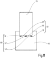
Fig. 11 ist eine weitere Ausführungsform einer Bauteilanordnung 30 dargestellt. Bei einem Einpressen der Gruppe 80 aus mehreren Kontaktelementen 32, 32', 32" in eine Gruppe 82 aus einer entsprechenden Anzahl von Aussparungen 12, 12', 12" bildet sich eine Mehrfach-Einpressverbindung aus. Jedes Kontaktelement 32, 32', 32" passt sich dabei jeder Aussparung 12 und jedem Kragenabschnitt 16 an, indem er sich verformt. Zwischen der Plattenelement 10 und dem Schienenabschnitt 78 entsteht eine Hochstromverbindung. Die vergrößerten Kontaktlängen der Kragenabschnitte ermöglichen es, sehr hohe Ströme weiter zu leiten. - In den
Fig. 12 und 13 ist eine weitere Ausführungsform einer Bauteilanordnung 30 dargestellt.Fig. 13 zeigt eine Detailansicht X in derFig. 12 . - Es sind mehre Kontaktelemente 32, 32', die separat voneinander ausgebildet sind, mit dem Plattenelement 10 verbunden. Unter Verwendung von Tiefziehen sind die Kragenabschnitte 16 derart ausgebildet, dass aus dem Plattenelement 10 durch Zugdruckumformen offene Kragenabschnitte 16 mit einem Innendurchmesser 26 und der Dicke 22 des Plattenelements 10 geformt werden. Die Tiefe 24 ist etwa doppelt so lang wie die Dicke 22,d. h. 24 kann hierbei 1,8 - mal bis 2,5 - mal so lang sein wie die Dicke 22. Ein Kontaktelement 32 weist zwei sich gegenüberliegenden gebogenen Schenkelabschnitte 34, 36 auf, die zwischen sich einen Schenkelspalt 35 frei lassen.
- In
Fig. 14 sind schematische Ablaufdiagramme eines nicht beanspruchten Verfahrens 60 zur Herstellung eines Plattenelements und eines nicht beanspruchten Verfahrens 62 zur Herstellung einer Bauteilanordnung dargestellt. - Das Verfahren 60 zur Herstellung eines Plattenelements beginnt in einem Startschritt 64, wobei zunächst in einem Schritt 66 ein Plattenelement bereitgestellt wird.
- In einem Schritt 68 werden dann durch Tiefziehen die Kragenabschnitte 16 und die Aussparungen 12 in dem Plattenelement 10 bereitgestellt. Grundsätzlich können die Aussparungen 12, insbesondere mit geringerem Durchmesser, auch schon vor dem Tiefziehen bereitgestellt werden, bspw. bei einem Gießen des Plattenelements oder auf andere Art vorab eingebracht werden. In jedem Fall werden die Kragenabschnitte 16 durch Tiefziehen ausgebildet. Dieses Verfahren endet dann in einem Stoppschritt 72. Grundsätzlich kann nach dem Tiefziehen vorgesehen sein, die Innenoberfläche 14 der Aussparungen 12 zu verzinnen.
- In dem Verfahren zum Herstellen einer Bauteilanordnung 62 werden zunächst auch die Schritte 64, 66, 68 und ggf. ein Verzinnen durchgeführt. Es erfolgt eine Bereitstellung eines voranstehend beschriebenen Kontaktelements mit mindestens zwei Schenkelabschnitten. Dieses Kontaktelement wird mit den Schenkelabschnitten 34, 36 bzw. zusätzlich 48, 50 in eine der mindestens einen Aussparungen 12 eingepresst. Grundsätzlich kann der Vorgang des Einpressens 70 wiederholt werden und so eine Mehrzahl von Kontaktelementen in jeweils eine Aussparung eingepresst werden. Auf diese Weise kann beispielsweise vorgesehen sein, dass wie in den
Fig. 2 und 3 dargestellt, neun Aussparungen vorgesehen sind und neun Kontaktelemente eingepresst werden, jeweils ein Kontaktelement in eine Aussparung. - Beim Verbindungsvorgang in dem Schritt des Einpressens 70 wird das Kontaktelement 32 beispielsweise mit einem Hub in ca. 0,1 Sekunden mit der jeweiligen Aussparung 12 und dem zugeordneten Kragenabschnitt 16 verbunden. Dadurch, dass ein Innendurchmesser 26 kleiner als ein Außendurchmesser 84 der Schenkabschnitte 34, 36 des Kontaktelements 32 ist, entsteht ein sehr hoher Einpressdruck, der ohne Temperatureinwirkung zu einer Verschweißung der Werkstoffe des Kontaktelements 32 und des Plattenelements 10 führen. Es entsteht eine direkte, elastische Verbindung mit einem sehr hohen spezifischen elektrischen Leitwert. Dadurch, dass sich eine Kontaktfläche aufgrund eines Kragenabschnitts 16 vergrößert hat, können beispielsweise bei einem 12 V Bordnetz in einem Kraftfahrzeug Ströme von beispielsweise 20 A und mehr weiter geleitet werden.
- Das Verfahren zur Herstellung einer Bauteilanordnung endet dann ebenfalls in einem Stoppschritt 72.
Claims (6)
- Bauteilanordnung (30) zur Stromführung mitmehreren Einpress-Kontaktelementen (32), die jeweils an mindestens einem Ende (37) mindestens zwei Schenkelabschnitte (34, 36, 48, 50) aufweisen und jeder Schenkelabschnitt (34, 36, 48, 50) nach außen gewölbte Seitenflächen (39) aufweist, wobei die mehreren Einpress-Kontaktelemente (32) über einen Schienenabschnitt (78) miteinander verbunden sind; undeinem Plattenelement (10) zur Stromführung, das eine Dicke (22) und mehrere kreisförmige Aussparungen (12) zur Bereitstellung einer Kontaktaufnahme für ein Einpress-Kontaktelement (32) aufweist, wobei jede Aussparung (12) auf zumindest einer Seite (21) des Plattenelements von einem Kragenabschnitt (16) umgeben ist;
wobeidie mindestens zwei Schenkelabschnitte (34, 36, 48, 50) in jeweils eine Aussparung (12) eingepresst sind und jeweils mit einer Innenoberfläche (14) der jeweiligen Aussparung (12) in Kontakt sind, wobei ein jeweiliger Scheitelpunkt (52, 54) einer Wölbung (46) mit der Innenoberfläche (14) in Kontakt ist;die Aussparungen und Kragenabschnitte durch Tiefziehen bereitgestellt sind;die Dicke des Plattenelements etwa 0,8mm beträgt, unddie Kragenabschnitte (16) sich von einer Oberfläche (20) des Plattenelements (10) aus mit einer Kragenabschnittshöhe (25) erstrecken, die im Bereich von 0,4 mm bis 1,6mm liegt. - Bauteilanordnung nach Anspruch 1, dadurch gekennzeichnet, dass der Kragenabschnitt (16) mit einem Radius (28) auf eine Oberfläche (20) des Plattenelements (10) übergeht.
- Bauteilanordnung nach einem der Ansprüche 1 bis 2, dadurch gekennzeichnet, dass die Aussparungen (12) jeweils als ein das Plattenelement (10) und den Kragenabschnitt (16) durchdringendes Durchgangsloch ausgebildet ist.
- Bauteilanordnung nach einem der Ansprüche 1 bis 3, dadurch gekennzeichnet, dass die Innenoberfläche (14) der Aussparungen (12) mit Zinn beschichtet ist.
- Bauteilanordnung nach Anspruch 1, dadurch gekennzeichnet, dass zumindest die mindestens zwei Schenkelabschnitte (34, 36, 48, 50) des Kontaktelements (32) aus Kupfer ausgebildet sind.
- Bauteilanordnung nach Anspruch 1 oder 5, dadurch gekennzeichnet, dass eine Oberfläche (38) der mindestens zwei Schenkelabschnitte (34, 36, 48, 50) mit Zinn beschichtet ist.
Applications Claiming Priority (3)
| Application Number | Priority Date | Filing Date | Title |
|---|---|---|---|
| DE102012022531 | 2012-11-14 | ||
| DE102013111963.8A DE102013111963A1 (de) | 2012-11-14 | 2013-10-30 | Plattenelement mit Tiefziehbohrung für Einpresskontakte |
| PCT/EP2013/073704 WO2014076122A1 (de) | 2012-11-14 | 2013-11-13 | Plattenelement mit tiefziehbohrung für einpresskontakte |
Publications (2)
| Publication Number | Publication Date |
|---|---|
| EP2920847A1 EP2920847A1 (de) | 2015-09-23 |
| EP2920847B1 true EP2920847B1 (de) | 2024-10-16 |
Family
ID=50555961
Family Applications (1)
| Application Number | Title | Priority Date | Filing Date |
|---|---|---|---|
| EP13791798.5A Active EP2920847B1 (de) | 2012-11-14 | 2013-11-13 | Plattenelement mit tiefziehbohrung für einpresskontakte |
Country Status (3)
| Country | Link |
|---|---|
| EP (1) | EP2920847B1 (de) |
| DE (1) | DE102013111963A1 (de) |
| WO (1) | WO2014076122A1 (de) |
Families Citing this family (6)
| Publication number | Priority date | Publication date | Assignee | Title |
|---|---|---|---|---|
| DE102014117410B4 (de) * | 2014-11-27 | 2019-01-03 | Heraeus Deutschland GmbH & Co. KG | Elektrisches Kontaktelement, Einpressstift, Buchse und Leadframe |
| DE102015100149A1 (de) | 2015-01-08 | 2016-07-14 | Raimund Huber | Elektrisches Funktionsbauteil mit Kontaktstift und Verfahren zur Herstellung eines elektrischen Funktionsbauteils |
| EP3016208B1 (de) * | 2015-08-24 | 2019-11-20 | Continental Teves AG & Co. OHG | Elektrische vorrichtung umfassend eine kontaktanordung und verfahren zur herstellung einer einfassung einer kontaktanordnung |
| DE102015119785B4 (de) | 2015-11-04 | 2020-03-26 | ept Holding GmbH & Co. KG | Lochkontur für Einpresstechnik in ein Stanzgitter |
| DE102016115173A1 (de) * | 2016-08-16 | 2018-02-22 | Abb Schweiz Ag | Dünner Leiter mit Durchgängen |
| DE102022134501A1 (de) * | 2022-12-22 | 2024-06-27 | Te Connectivity Solutions Gmbh | Gehäuseelement für eine elektronische Schaltung |
Citations (4)
| Publication number | Priority date | Publication date | Assignee | Title |
|---|---|---|---|---|
| EP1391965A1 (de) * | 2002-08-22 | 2004-02-25 | Wago Verwaltungsgesellschaft mbH | Federkraftklemmanschluss für einen elektrischen Leiter |
| US20050204538A1 (en) * | 2004-03-19 | 2005-09-22 | Epic Technology Inc. | Contact and method for making same |
| US20080166928A1 (en) * | 2007-01-10 | 2008-07-10 | Liang Tang | Compliant pin |
| US20130143433A1 (en) * | 2010-08-09 | 2013-06-06 | Phoenix Contact Gmbh & Co. Kg | Connection terminal |
Family Cites Families (3)
| Publication number | Priority date | Publication date | Assignee | Title |
|---|---|---|---|---|
| DE102004006533A1 (de) | 2004-02-11 | 2005-09-01 | Conti Temic Microelectronic Gmbh | Elektrisch leitfähiger Kontaktstift zum Einpressen in eine Öffnung einer Leiterplatte sowie elektrische Baugruppe mit einem solchen Kontaktstift |
| DE102004006575A1 (de) | 2004-02-11 | 2005-09-01 | Leopold Kostal Gmbh & Co Kg | Leistungsverteiler für ein Kraftfahrzeug |
| DE102008024366B4 (de) * | 2008-05-20 | 2010-11-25 | Phoenix Contact Gmbh & Co. Kg | Durchführungsklemme |
-
2013
- 2013-10-30 DE DE102013111963.8A patent/DE102013111963A1/de active Pending
- 2013-11-13 EP EP13791798.5A patent/EP2920847B1/de active Active
- 2013-11-13 WO PCT/EP2013/073704 patent/WO2014076122A1/de not_active Ceased
Patent Citations (4)
| Publication number | Priority date | Publication date | Assignee | Title |
|---|---|---|---|---|
| EP1391965A1 (de) * | 2002-08-22 | 2004-02-25 | Wago Verwaltungsgesellschaft mbH | Federkraftklemmanschluss für einen elektrischen Leiter |
| US20050204538A1 (en) * | 2004-03-19 | 2005-09-22 | Epic Technology Inc. | Contact and method for making same |
| US20080166928A1 (en) * | 2007-01-10 | 2008-07-10 | Liang Tang | Compliant pin |
| US20130143433A1 (en) * | 2010-08-09 | 2013-06-06 | Phoenix Contact Gmbh & Co. Kg | Connection terminal |
Also Published As
| Publication number | Publication date |
|---|---|
| WO2014076122A1 (de) | 2014-05-22 |
| DE102013111963A1 (de) | 2014-05-15 |
| EP2920847A1 (de) | 2015-09-23 |
Similar Documents
| Publication | Publication Date | Title |
|---|---|---|
| EP2899812B1 (de) | Verbindungsanordnung an Leiterplatten | |
| EP2441129B1 (de) | Einpresskontakt zur verbindung eines elektronischen bauelementes mit einer leiterplatte sowie einpresswerkzeug und verfahren zur herstellung eines einpresskontaktes | |
| EP2920847B1 (de) | Plattenelement mit tiefziehbohrung für einpresskontakte | |
| DE102011122371A1 (de) | Elektrische Anschlusseinrichtung zur Herstellung einer Lötverbindung | |
| EP3477781A1 (de) | Steckerbuchse für leiterplatinen | |
| DE102013209407A1 (de) | Verfahren zur lötfreien elektrischen Einpresskontaktierung von elektrisch leitfähigen Einpress-Stiften in Leiterplatten | |
| EP1754285B1 (de) | Einpresskontakt | |
| EP3022805A1 (de) | Kontakteinrichtung zum herstellen einer elektrischen verbindung mit einer kontaktstelle einer leiterplatte | |
| EP3192130B1 (de) | Verfahren zur lötfreien elektrischen einpresskontaktierung von elektrisch leitfähigen einpress-stiften in leiterplatten | |
| EP3243246B1 (de) | Elektrisches funktionsbauteil mit kontaktstift und verfahren zur herstellung eines elektrischen funktionsbauteils | |
| EP2705578A1 (de) | Elektrisches kontaktelement | |
| DE102013013368B4 (de) | Verfahren zur Herstellung einer elektrischen Verbindung sowie elektrische Verbindung | |
| DE102012218433B4 (de) | Kontaktanordnung | |
| EP2700126A2 (de) | Hochstromkontaktelement für leiterplatten | |
| EP2732508B1 (de) | Direktsteckelement mit integrierter verriegelung | |
| EP1912295A1 (de) | Stromschiene | |
| EP2109186B1 (de) | Verfahren zur Herstellung einer elektrischen Verbindung zwischen einer Stromschiene und einer Leiterplatte | |
| EP4094326B1 (de) | Verbindungsanordnung und verfahren zum verbinden einer verbindungsanordnung mit einem bauteil | |
| DE102015119785B4 (de) | Lochkontur für Einpresstechnik in ein Stanzgitter | |
| DE102004041169B3 (de) | Anordnung und Verfahren zur Masseanbindung eines elektrischen Schaltungsträgers | |
| EP1363362A1 (de) | Umformen von Leiterenden eines Flachbandkabels | |
| DE102006000958B4 (de) | Elektrisches Gerät | |
| WO2009003907A1 (de) | Steckverbinder | |
| DE102016116375B4 (de) | Kontaktierungsvorrichtung | |
| EP1162694B1 (de) | Vorrichtung zum Verbinden von elektrischen Leitern |
Legal Events
| Date | Code | Title | Description |
|---|---|---|---|
| PUAI | Public reference made under article 153(3) epc to a published international application that has entered the european phase |
Free format text: ORIGINAL CODE: 0009012 |
|
| 17P | Request for examination filed |
Effective date: 20150611 |
|
| AK | Designated contracting states |
Kind code of ref document: A1 Designated state(s): AL AT BE BG CH CY CZ DE DK EE ES FI FR GB GR HR HU IE IS IT LI LT LU LV MC MK MT NL NO PL PT RO RS SE SI SK SM TR |
|
| AX | Request for extension of the european patent |
Extension state: BA ME |
|
| DAX | Request for extension of the european patent (deleted) | ||
| STAA | Information on the status of an ep patent application or granted ep patent |
Free format text: STATUS: EXAMINATION IS IN PROGRESS |
|
| 17Q | First examination report despatched |
Effective date: 20170926 |
|
| RAP3 | Party data changed (applicant data changed or rights of an application transferred) |
Owner name: IWIS MECHATRONICS GMBH & CO. KG |
|
| P01 | Opt-out of the competence of the unified patent court (upc) registered |
Effective date: 20230724 |
|
| GRAP | Despatch of communication of intention to grant a patent |
Free format text: ORIGINAL CODE: EPIDOSNIGR1 |
|
| STAA | Information on the status of an ep patent application or granted ep patent |
Free format text: STATUS: GRANT OF PATENT IS INTENDED |
|
| INTG | Intention to grant announced |
Effective date: 20240513 |
|
| GRAS | Grant fee paid |
Free format text: ORIGINAL CODE: EPIDOSNIGR3 |
|
| GRAA | (expected) grant |
Free format text: ORIGINAL CODE: 0009210 |
|
| STAA | Information on the status of an ep patent application or granted ep patent |
Free format text: STATUS: THE PATENT HAS BEEN GRANTED |
|
| AK | Designated contracting states |
Kind code of ref document: B1 Designated state(s): AL AT BE BG CH CY CZ DE DK EE ES FI FR GB GR HR HU IE IS IT LI LT LU LV MC MK MT NL NO PL PT RO RS SE SI SK SM TR |
|
| REG | Reference to a national code |
Ref country code: GB Ref legal event code: FG4D Free format text: NOT ENGLISH |
|
| REG | Reference to a national code |
Ref country code: DE Ref legal event code: R096 Ref document number: 502013016548 Country of ref document: DE Ref country code: CH Ref legal event code: EP |
|
| REG | Reference to a national code |
Ref country code: IE Ref legal event code: FG4D Free format text: LANGUAGE OF EP DOCUMENT: GERMAN |
|
| PGFP | Annual fee paid to national office [announced via postgrant information from national office to epo] |
Ref country code: DE Payment date: 20241206 Year of fee payment: 12 |
|
| REG | Reference to a national code |
Ref country code: LT Ref legal event code: MG9D |
|
| REG | Reference to a national code |
Ref country code: NL Ref legal event code: MP Effective date: 20241016 |
|
| PG25 | Lapsed in a contracting state [announced via postgrant information from national office to epo] |
Ref country code: NL Free format text: LAPSE BECAUSE OF FAILURE TO SUBMIT A TRANSLATION OF THE DESCRIPTION OR TO PAY THE FEE WITHIN THE PRESCRIBED TIME-LIMIT Effective date: 20241016 |
|
| PG25 | Lapsed in a contracting state [announced via postgrant information from national office to epo] |
Ref country code: NL Free format text: LAPSE BECAUSE OF FAILURE TO SUBMIT A TRANSLATION OF THE DESCRIPTION OR TO PAY THE FEE WITHIN THE PRESCRIBED TIME-LIMIT Effective date: 20241016 |
|
| PG25 | Lapsed in a contracting state [announced via postgrant information from national office to epo] |
Ref country code: IS Free format text: LAPSE BECAUSE OF FAILURE TO SUBMIT A TRANSLATION OF THE DESCRIPTION OR TO PAY THE FEE WITHIN THE PRESCRIBED TIME-LIMIT Effective date: 20250216 Ref country code: PT Free format text: LAPSE BECAUSE OF FAILURE TO SUBMIT A TRANSLATION OF THE DESCRIPTION OR TO PAY THE FEE WITHIN THE PRESCRIBED TIME-LIMIT Effective date: 20250217 Ref country code: HR Free format text: LAPSE BECAUSE OF FAILURE TO SUBMIT A TRANSLATION OF THE DESCRIPTION OR TO PAY THE FEE WITHIN THE PRESCRIBED TIME-LIMIT Effective date: 20241016 |
|
| PG25 | Lapsed in a contracting state [announced via postgrant information from national office to epo] |
Ref country code: FI Free format text: LAPSE BECAUSE OF FAILURE TO SUBMIT A TRANSLATION OF THE DESCRIPTION OR TO PAY THE FEE WITHIN THE PRESCRIBED TIME-LIMIT Effective date: 20241016 |
|
| PG25 | Lapsed in a contracting state [announced via postgrant information from national office to epo] |
Ref country code: BG Free format text: LAPSE BECAUSE OF FAILURE TO SUBMIT A TRANSLATION OF THE DESCRIPTION OR TO PAY THE FEE WITHIN THE PRESCRIBED TIME-LIMIT Effective date: 20241016 |
|
| PG25 | Lapsed in a contracting state [announced via postgrant information from national office to epo] |
Ref country code: ES Free format text: LAPSE BECAUSE OF FAILURE TO SUBMIT A TRANSLATION OF THE DESCRIPTION OR TO PAY THE FEE WITHIN THE PRESCRIBED TIME-LIMIT Effective date: 20241016 |
|
| PG25 | Lapsed in a contracting state [announced via postgrant information from national office to epo] |
Ref country code: NO Free format text: LAPSE BECAUSE OF FAILURE TO SUBMIT A TRANSLATION OF THE DESCRIPTION OR TO PAY THE FEE WITHIN THE PRESCRIBED TIME-LIMIT Effective date: 20250116 |
|
| PG25 | Lapsed in a contracting state [announced via postgrant information from national office to epo] |
Ref country code: GR Free format text: LAPSE BECAUSE OF FAILURE TO SUBMIT A TRANSLATION OF THE DESCRIPTION OR TO PAY THE FEE WITHIN THE PRESCRIBED TIME-LIMIT Effective date: 20250117 Ref country code: LV Free format text: LAPSE BECAUSE OF FAILURE TO SUBMIT A TRANSLATION OF THE DESCRIPTION OR TO PAY THE FEE WITHIN THE PRESCRIBED TIME-LIMIT Effective date: 20241016 |
|
| PG25 | Lapsed in a contracting state [announced via postgrant information from national office to epo] |
Ref country code: PL Free format text: LAPSE BECAUSE OF FAILURE TO SUBMIT A TRANSLATION OF THE DESCRIPTION OR TO PAY THE FEE WITHIN THE PRESCRIBED TIME-LIMIT Effective date: 20241016 |
|
| PG25 | Lapsed in a contracting state [announced via postgrant information from national office to epo] |
Ref country code: RS Free format text: LAPSE BECAUSE OF FAILURE TO SUBMIT A TRANSLATION OF THE DESCRIPTION OR TO PAY THE FEE WITHIN THE PRESCRIBED TIME-LIMIT Effective date: 20250116 |
|
| REG | Reference to a national code |
Ref country code: CH Ref legal event code: PL |
|
| PG25 | Lapsed in a contracting state [announced via postgrant information from national office to epo] |
Ref country code: SM Free format text: LAPSE BECAUSE OF FAILURE TO SUBMIT A TRANSLATION OF THE DESCRIPTION OR TO PAY THE FEE WITHIN THE PRESCRIBED TIME-LIMIT Effective date: 20241016 |
|
| PG25 | Lapsed in a contracting state [announced via postgrant information from national office to epo] |
Ref country code: MC Free format text: LAPSE BECAUSE OF FAILURE TO SUBMIT A TRANSLATION OF THE DESCRIPTION OR TO PAY THE FEE WITHIN THE PRESCRIBED TIME-LIMIT Effective date: 20241016 |
|
| PG25 | Lapsed in a contracting state [announced via postgrant information from national office to epo] |
Ref country code: DK Free format text: LAPSE BECAUSE OF FAILURE TO SUBMIT A TRANSLATION OF THE DESCRIPTION OR TO PAY THE FEE WITHIN THE PRESCRIBED TIME-LIMIT Effective date: 20241016 |
|
| PG25 | Lapsed in a contracting state [announced via postgrant information from national office to epo] |
Ref country code: LU Free format text: LAPSE BECAUSE OF NON-PAYMENT OF DUE FEES Effective date: 20241113 |
|
| REG | Reference to a national code |
Ref country code: CH Ref legal event code: PL |
|
| REG | Reference to a national code |
Ref country code: DE Ref legal event code: R097 Ref document number: 502013016548 Country of ref document: DE |
|
| PG25 | Lapsed in a contracting state [announced via postgrant information from national office to epo] |
Ref country code: EE Free format text: LAPSE BECAUSE OF FAILURE TO SUBMIT A TRANSLATION OF THE DESCRIPTION OR TO PAY THE FEE WITHIN THE PRESCRIBED TIME-LIMIT Effective date: 20241016 |
|
| PG25 | Lapsed in a contracting state [announced via postgrant information from national office to epo] |
Ref country code: CH Free format text: LAPSE BECAUSE OF NON-PAYMENT OF DUE FEES Effective date: 20241130 |
|
| PG25 | Lapsed in a contracting state [announced via postgrant information from national office to epo] |
Ref country code: RO Free format text: LAPSE BECAUSE OF FAILURE TO SUBMIT A TRANSLATION OF THE DESCRIPTION OR TO PAY THE FEE WITHIN THE PRESCRIBED TIME-LIMIT Effective date: 20241016 |
|
| PG25 | Lapsed in a contracting state [announced via postgrant information from national office to epo] |
Ref country code: SK Free format text: LAPSE BECAUSE OF FAILURE TO SUBMIT A TRANSLATION OF THE DESCRIPTION OR TO PAY THE FEE WITHIN THE PRESCRIBED TIME-LIMIT Effective date: 20241016 |
|
| PG25 | Lapsed in a contracting state [announced via postgrant information from national office to epo] |
Ref country code: CZ Free format text: LAPSE BECAUSE OF FAILURE TO SUBMIT A TRANSLATION OF THE DESCRIPTION OR TO PAY THE FEE WITHIN THE PRESCRIBED TIME-LIMIT Effective date: 20241016 |
|
| PG25 | Lapsed in a contracting state [announced via postgrant information from national office to epo] |
Ref country code: IT Free format text: LAPSE BECAUSE OF FAILURE TO SUBMIT A TRANSLATION OF THE DESCRIPTION OR TO PAY THE FEE WITHIN THE PRESCRIBED TIME-LIMIT Effective date: 20241016 |
|
| PLBE | No opposition filed within time limit |
Free format text: ORIGINAL CODE: 0009261 |
|
| STAA | Information on the status of an ep patent application or granted ep patent |
Free format text: STATUS: NO OPPOSITION FILED WITHIN TIME LIMIT |
|
| REG | Reference to a national code |
Ref country code: BE Ref legal event code: MM Effective date: 20241130 |
|
| PG25 | Lapsed in a contracting state [announced via postgrant information from national office to epo] |
Ref country code: SE Free format text: LAPSE BECAUSE OF FAILURE TO SUBMIT A TRANSLATION OF THE DESCRIPTION OR TO PAY THE FEE WITHIN THE PRESCRIBED TIME-LIMIT Effective date: 20241016 |
|
| 26N | No opposition filed |
Effective date: 20250717 |
|
| GBPC | Gb: european patent ceased through non-payment of renewal fee |
Effective date: 20250116 |
|
| PG25 | Lapsed in a contracting state [announced via postgrant information from national office to epo] |
Ref country code: BE Free format text: LAPSE BECAUSE OF NON-PAYMENT OF DUE FEES Effective date: 20241130 Ref country code: GB Free format text: LAPSE BECAUSE OF NON-PAYMENT OF DUE FEES Effective date: 20250116 |
|
| REG | Reference to a national code |
Ref country code: DE Ref legal event code: R082 Ref document number: 502013016548 Country of ref document: DE Representative=s name: PATENTANWAELTE BREGENZER UND REULE PARTNERSCHA, DE |
|
| PG25 | Lapsed in a contracting state [announced via postgrant information from national office to epo] |
Ref country code: FR Free format text: LAPSE BECAUSE OF NON-PAYMENT OF DUE FEES Effective date: 20241216 |
|
| PG25 | Lapsed in a contracting state [announced via postgrant information from national office to epo] |
Ref country code: IE Free format text: LAPSE BECAUSE OF NON-PAYMENT OF DUE FEES Effective date: 20241113 |