EP3837720B1 - Supraleitendes quantenrechenschaltungspaket - Google Patents
Supraleitendes quantenrechenschaltungspaket Download PDFInfo
- Publication number
- EP3837720B1 EP3837720B1 EP19758454.3A EP19758454A EP3837720B1 EP 3837720 B1 EP3837720 B1 EP 3837720B1 EP 19758454 A EP19758454 A EP 19758454A EP 3837720 B1 EP3837720 B1 EP 3837720B1
- Authority
- EP
- European Patent Office
- Prior art keywords
- substrate
- quantum computing
- computing circuit
- cover
- projections
- Prior art date
- Legal status (The legal status is an assumption and is not a legal conclusion. Google has not performed a legal analysis and makes no representation as to the accuracy of the status listed.)
- Active
Links
Images



Classifications
-
- H—ELECTRICITY
- H10—SEMICONDUCTOR DEVICES; ELECTRIC SOLID-STATE DEVICES NOT OTHERWISE PROVIDED FOR
- H10N—ELECTRIC SOLID-STATE DEVICES NOT OTHERWISE PROVIDED FOR
- H10N69/00—Integrated devices, or assemblies of multiple devices, comprising at least one superconducting element covered by group H10N60/00
-
- G—PHYSICS
- G06—COMPUTING OR CALCULATING; COUNTING
- G06N—COMPUTING ARRANGEMENTS BASED ON SPECIFIC COMPUTATIONAL MODELS
- G06N10/00—Quantum computing, i.e. information processing based on quantum-mechanical phenomena
- G06N10/20—Models of quantum computing, e.g. quantum circuits or universal quantum computers
-
- G—PHYSICS
- G06—COMPUTING OR CALCULATING; COUNTING
- G06N—COMPUTING ARRANGEMENTS BASED ON SPECIFIC COMPUTATIONAL MODELS
- G06N10/00—Quantum computing, i.e. information processing based on quantum-mechanical phenomena
- G06N10/40—Physical realisations or architectures of quantum processors or components for manipulating qubits, e.g. qubit coupling or qubit control
-
- H—ELECTRICITY
- H10—SEMICONDUCTOR DEVICES; ELECTRIC SOLID-STATE DEVICES NOT OTHERWISE PROVIDED FOR
- H10N—ELECTRIC SOLID-STATE DEVICES NOT OTHERWISE PROVIDED FOR
- H10N60/00—Superconducting devices
- H10N60/10—Junction-based devices
- H10N60/12—Josephson-effect devices
-
- H—ELECTRICITY
- H10—SEMICONDUCTOR DEVICES; ELECTRIC SOLID-STATE DEVICES NOT OTHERWISE PROVIDED FOR
- H10N—ELECTRIC SOLID-STATE DEVICES NOT OTHERWISE PROVIDED FOR
- H10N60/00—Superconducting devices
- H10N60/80—Constructional details
- H10N60/805—Constructional details for Josephson-effect devices
-
- H—ELECTRICITY
- H10—SEMICONDUCTOR DEVICES; ELECTRIC SOLID-STATE DEVICES NOT OTHERWISE PROVIDED FOR
- H10N—ELECTRIC SOLID-STATE DEVICES NOT OTHERWISE PROVIDED FOR
- H10N60/00—Superconducting devices
- H10N60/80—Constructional details
- H10N60/81—Containers; Mountings
-
- H—ELECTRICITY
- H10—SEMICONDUCTOR DEVICES; ELECTRIC SOLID-STATE DEVICES NOT OTHERWISE PROVIDED FOR
- H10N—ELECTRIC SOLID-STATE DEVICES NOT OTHERWISE PROVIDED FOR
- H10N60/00—Superconducting devices
- H10N60/80—Constructional details
- H10N60/81—Containers; Mountings
- H10N60/815—Containers; Mountings for Josephson-effect devices
-
- H—ELECTRICITY
- H10—SEMICONDUCTOR DEVICES; ELECTRIC SOLID-STATE DEVICES NOT OTHERWISE PROVIDED FOR
- H10N—ELECTRIC SOLID-STATE DEVICES NOT OTHERWISE PROVIDED FOR
- H10N60/00—Superconducting devices
- H10N60/80—Constructional details
- H10N60/82—Current path
-
- B—PERFORMING OPERATIONS; TRANSPORTING
- B82—NANOTECHNOLOGY
- B82Y—SPECIFIC USES OR APPLICATIONS OF NANOSTRUCTURES; MEASUREMENT OR ANALYSIS OF NANOSTRUCTURES; MANUFACTURE OR TREATMENT OF NANOSTRUCTURES
- B82Y10/00—Nanotechnology for information processing, storage or transmission, e.g. quantum computing or single electron logic
Definitions
- This invention relates to a superconducting quantum computing circuit package, in particular to a superconducting quantum computing circuit package including a holder for a substrate of the superconducting quantum computing circuit.
- EM electromagnetic
- a rectangular chip enclosed in conducting material, and having side lengths greater than a few millimetres (and both greater than the thickness) and a high dielectric permittivity of around 10 can support EM modes in the range of several to several tens of gigahertz.
- Such electromagnetic "chip-like” modes are almost always unwanted, particularly in the frequency range of several to several tens of gigahertz. These frequencies are similar to the desired operational frequencies of quantum computing circuits and thus they can interfere with the operation of a quantum computing circuit, through interactions with "circuit-like” modes, e.g. qubit modes, other circuit elements and control signals that are used. This can result in the loss of coherence in the circuit, which is important to maintain in order to prolong the operational lifetime of the circuit such that effective quantum processing can be performed.
- circuit-like modes e.g. qubit modes, other circuit elements and control signals that are used.
- One way to attempt to suppress spurious chip modes and cross-talk is to form vias which extend through the thickness of the substrate of a circuit. This introduces conductors among the circuit elements which act to disrupt and suppress the spurious chip modes by reducing the effective length scale over which standing waves may form in the chip, and also reduces cross-talk (e.g. between qubits) by providing conductors between the circuit elements, which can screen their field (e.g. capacitive and/or inductive) interactions.
- US 9836699 B1 relates to a microwave integrated quantum circuits with interposer.
- the aim of the invention is to provide a device which provides a cleaner frequency space for the operation of quantum computing circuits.
- the invention When viewed from a first aspect the invention provides a superconducting quantum computing circuit package in accordance with claim 1.
- the present invention provides a superconducting quantum computing circuit package.
- the package includes a substrate, a holder for the substrate and a cover on the opposite side of the substrate from the holder.
- the substrate has a superconducting quantum computing circuit formed on, e.g., its surface, with the circuit including multiple circuit elements such as qubits.
- One or more holes are formed to extend (all the way) through the substrate, with the holes being arranged among (e.g. two or more of) the circuit elements.
- the substrate is located on a surface of the holder, which is formed from a metal and/or superconductor.
- the holder has one or more projections that are formed on and project from the surface on which the substrate is received.
- the one or more projections on the holder correspond to the one or more holes in the substrate such that the projection(s) protrude through the holes to contact the (inside surface of the) cover (when the cover is placed on the holder), such that the projections pass through the thickness of the substrate among the plurality of circuit elements.
- This current path between the holder and the cover, via the projection(s) acts to acts to break up the formation of standing waves in the chip (e.g. across the whole area of the chip), suppressing (e.g.
- the separate substrate and holder of the package allow conducting elements (i.e. the projections of the holder) to be provided among the circuit elements of the quantum computing circuit.
- the presence of the projections reduces the length scale over which standing waves may be set up, thus increasing the frequency of the lowest frequency EM modes. This helps to suppress (e.g. substantially eliminate) EM chip-like modes being set up having frequencies that are similar to the desired operational frequencies of the quantum computing circuit. This helps to reduce the interference between unwanted chip-like modes and the quantum computing circuit during operation.
- the presence of the holes and projections among the circuit elements also helps to confine chip-like modes (e.g. modes that are substantially within a "chip", i.e. the substrate and the circuit formed thereon) and circuit-like modes (e.g. qubit modes, resonator modes, control lines modes, etc.) that are established to certain regions of the package and thus the quantum computing circuit, e.g. between the projections. This can help to improve the addressability (ability to be addressed independently) of the circuit elements and to reduce unwanted interactions (e.g. qubit cross-talk) in the quantum computing circuit during operation.
- chip-like modes e.g. modes that are substantially within a "chip", i.e. the substrate and the circuit formed thereon
- circuit-like modes e.g. qubit modes, resonator modes, control lines modes, etc.
- This can help to improve the addressability (ability to be addressed independently) of the circuit elements and to reduce unwanted interactions (e.g. qubit cross-talk) in the quantum computing circuit during operation.
- the separate holder, cover and substrate also help to minimise the number of fabrication steps required in the manufacture of the substrate and the quantum computing circuit.
- the substrate, holder and cover are formed as discrete components.
- the holder and cover may be manufactured separately from the substrate (and from each other), such that the substrate may simply require holes to be formed through its thickness. This helps to minimise the number of defects and impurities in these parts.
- the reduced interference, cross-talk and presence of impurities and defects in the quantum computing circuit all help to provide a clean electromagnetic environment for the quantum computing circuit to operate in, as well as enabling quantum computing circuits to be scaled onto larger chips with a larger number of, e.g., qubits without increasing the number of spurious EM mode interactions. This helps to prolong the coherence of the quantum computing circuit elements during operation, therefore improving the conditions for performing quantum computing calculations.
- the arrangement of the present invention provides a number of benefits over a substrate containing integrally formed vias. This is because vias are only able to remove chip like modes. Therefore if there are gaps between an enclosure surrounding the chip and the chip, spurious modes can exist in these gaps that could still interfere with the quantum computing circuit, which are not removed by vias. With the projections of the holder of the present invention passing through the holes in the substrate and contacting the cover, the projections pass through any gap regions in the vicinity of the qubits, protecting them from spurious gap modes as well.
- the substrate may be any suitable and desired substrate for forming a superconducting quantum computing circuit on the substrate, e.g. for use in a superconducting environment.
- the substrate comprises a high dielectric substrate.
- the substrate may be formed from any suitable and desired material, e.g. silicon or sapphire.
- the substrate may be any suitable and desired shape.
- the substrate is substantially planar (other than the holes extending through the thickness of the substrate).
- the plurality of circuit elements of the quantum computing circuit may comprise any suitable and desired circuit elements.
- the plurality of circuit elements comprises one or more (e.g. all) of: a qubit (e.g. comprising a Josephson junction and superconducting electrodes), a control line and a readout element (e.g. resonator).
- a qubit e.g. comprising a Josephson junction and superconducting electrodes
- a control line and a readout element e.g. resonator
- the plurality of circuit elements comprises a plurality of sets of a qubit, a control line and a readout element.
- the circuit elements may be arranged in any suitable and desired way, e.g.
- the arrangement of the quantum computing circuit package of the present invention is suited to including such a layout of a quantum computing circuit.
- the plurality of circuit elements comprises a plurality of qubits and, e.g., control lines and readout elements.
- the qubits may be any suitable and desired size, and may be spaced from each other by any suitable and desired distance.
- the qubits have a maximum dimension of between 0.1 mm and 1 mm.
- the plurality of qubits are spaced from adjacent qubits by between 0.2 mm and 2 mm.
- the circuit elements of the quantum computing circuit are preferably formed on a surface of the substrate.
- the thickness of the substrate is significantly smaller than its other two dimensions (e.g. length and width), e.g. in directions perpendicular to the thickness of the substrate.
- the substrate has two faces on opposite sides of the substrate (separated by the thickness of the substrate) on which circuit elements may be formed. Preferably one of these faces is directed towards the surface of the holder when the substrate is placed onto the holder.
- the circuit elements are formed only on one face of the substrate, e.g. the face opposite the surface of the holder. In another embodiment the circuit elements are formed on both faces of the substrate. It will be appreciated that the design of the package allows for this owing to the separation of the conducting elements (i.e. the projections of the holder) from the substrate. In contrast, a substrate containing vias (which are provided integrally in the substrate) may allow for circuit elements to be provided on both sides of a substrate; however, this would require a complicated multistage fabrication process. The package design of the present invention thus remains compatible with a wide range of circuit designs.
- the substrate is not fixedly attached (e.g. glued or bonded) to the holder or the cover in the package.
- the (e.g. face of the) substrate may simply rest on the surface of the holder and/or the cover. This again helps to allow, in some embodiments, the circuit elements of the quantum computing circuit to be formed on the face of the substrate that faces the surface of the holder (and thus, for example, on both faces of the substrate).
- the holder and the cover may be formed from any suitable and desired metal and/or superconductor, e.g. a superconducting metal.
- a superconducting metal e.g. aluminium.
- the holder may be any suitable and desired shape for receiving the substrate.
- the surface for receiving the substrate is substantially planar (other than the projections).
- the holder is substantially cuboid.
- the surface for receiving the substrate is recessed from a face of the holder, e.g. from a face of the cuboid.
- the holder may comprise a rim around (and projecting above) the surface for receiving the substrate.
- the surface may be recessed by any suitable and desired depth.
- the surface is recessed from the face of the holder by a depth substantially equal to the thickness of the substrate, e.g. the rim has a height substantially equal to the thickness of the substrate.
- the (e.g. outer surface of the) substrate lies substantially flush with the face of the holder (and, e.g., the rim).
- the projections arranged on the surface project in a direction substantially perpendicular to the (e.g. planar) surface.
- the holes in the substrate extend in a direction substantially perpendicular to the surface (e.g. face) of the substrate.
- the one or more projections on the surface of the holder may be any suitable and desired shape, dimensions and spacing from each other. Preferably there are a plurality of projections arranged on and projecting from the surface.
- the projections may be arranged relative (e.g. in position and/or number) to the circuit elements (e.g. qubits) in any suitable and desired way.
- the holder comprises at least as many projections as the number of qubits in the quantum computing circuit on the substrate.
- the projections are arranged such that there are a plurality of circuit elements (e.g. qubits) between each projection. Thus, for example, there may be at least as many circuit elements (e.g. qubits) as projections.
- the hole(s) in the substrate correspond in shape and (slightly larger) size to the projection(s) of the holder, so that the hole(s) receive the projection(s) when the substrate is placed on the holder.
- the substrate may comprise at least as many holes as the number of qubits in the quantum computing circuit on the substrate.
- the holes are arranged such that there are a plurality of circuit elements (e.g. qubits) between each hole.
- the substrate comprises an equal number of holes to the number of projections on the surface of the holder.
- the one or more holes may be arranged among the plurality of circuit elements in any suitable and desired way, e.g. in a configuration that acts to suppress chip-like modes in the frequency range of operation of the quantum computing circuit.
- the one or more holes are arranged between the plurality of circuit elements, wherein the one or more projections protrude through at least part of the thickness of the substrate between the plurality of circuit elements.
- the one or more holes are arranged among (e.g. between (e.g. to intersperse)) the qubits of the quantum computing circuit formed on the substrate.
- the one or more projections are arranged to pass between the (e.g. adjacent) qubits. This helps to reduce unwanted interactions between circuit-like modes (e.g. to reduce the cross-talk between adjacent qubits) in addition to the suppression of the spurious electromagnetic modes.
- the projections are arranged in a (e.g. regular geometric) grid, e.g. corresponding to a (e.g. regular geometric) grid of qubits in the quantum computing circuit.
- the holes and the corresponding projections may be arranged in any suitable and desired configuration such that they suppress the chip-like and, e.g., circuit-like modes in the operational frequency range of the quantum computing circuit, e.g. to confine the modes to the vicinity of individual qubits (such that the modes do not extend over plural qubits).
- the maximum spacing between adjacent holes and/or projections corresponds to (e.g. would be able to support) a chip-like mode having a frequency (e.g. significantly) greater than the maximum operational frequency of the quantum computing circuit.
- the arrangement (e.g. size and spacing) of the projections and the corresponding holes is related to (e.g. matches) the arrangement (e.g. size and spacing) of the circuit elements (e.g. qubits) of the quantum computing circuit on the substrate.
- the plurality of projections are spaced from adjacent projections by between 0.2 mm and 2 mm (and similarly for the holes to accommodate the corresponding projections).
- the one or more projections are (e.g. each) between 0.2 mm and 1 mm (e.g. approximately 0.5 mm) in height (i.e. in the direction in which they project from the surface of the holder).
- the one or more projections may extend part way through the thickness of the substrate and the cover may comprise corresponding projections (projecting from a surface of the cover) that also extend part way through the thickness of the substrate (from the other side of the substrate), such that the one or more projections of the holder contact the corresponding one or more projections of the cover.
- the cover comprises one or more projections
- the optional and preferable features outlined herein with respect to the one or more projections of the holder may also apply to the one or more projections of the cover.
- the height of the projection(s) may depend on how far the projection(s) project through the substrate.
- the one or more projections e.g. each
- the one or more projections extend all the way through the thickness of the substrate to contact the cover.
- the height of the one or more projections is (e.g. each) greater than or equal to the thickness of the substrate. The Applicant has found that when the projections extend all the way through the thickness of the substrate, this may be particularly effective in suppressing (e.g. substantially eliminating) electromagnetic modes in the operational frequency range of the quantum computing circuit.
- the depth of the recess or height of the rim is substantially equal to the height of the one or more projections.
- the depth of the recess or height of the rim is between 0.2 mm and 1 mm (e.g. approximately 0.5 mm).
- the one or more projections are (e.g. each) between 0.2 mm and 1 mm (e.g. approximately 0.5 mm) in width (i.e. in the direction parallel to the surface of the holder).
- the one or more holes are (e.g. each) between 0.2 mm and 1 mm (e.g. approximately 0.5 mm) in width (i.e. in the direction parallel to the face of the substrate).
- the one or more projections and the (corresponding) one or more holes are (e.g. each) substantially cylindrical.
- the one or more projections e.g. each
- the one or more holes have a cross-section (in a plane substantially parallel to the surface of the holder) that is substantially constant in the direction in which the one or more projections project, e.g. in a direction substantially perpendicular to the surface of the holder.
- the one or more holes e.g. each
- the one or more projections may (e.g. each) take the form of a wall or a pillar and the (corresponding) one or more holes may (e.g. each) take the form of a channel or a pillar-shaped hole.
- the one or more projections and the one or more holes (e.g. each) have a circular cross-section (and thus the axis of the cylinder of a projection or a hole) that is arranged in a direction substantially perpendicular to the surface of the holder or to the face of the substrate (i.e. substantially parallel to the thickness of the substrate).
- the distal end of (e.g. each of) the one or more projections is tapered, e.g. rounded or pointed. This helps to ensure that the distal end(s) of the one or more projections contact the cover.
- the Applicant has appreciated, at least in some embodiments of the present invention, that small gaps between the projection(s) and the cover may cause problems in not suppressing the modes. For example, a gap as small as 1 ⁇ m may cause a problem.
- the one or more projections may be arranged (e.g. shaped, sized and/or positioned) to suppress (e.g. substantially eliminate) any suitable and desired electromagnetic (e.g. chip-like) modes in the frequency range of operation of the quantum computing circuit.
- the one or more projections are arranged to suppress (e.g. substantially eliminate) all electromagnetic (e.g. chip-like) modes in the frequency range of operation of the quantum computing circuit.
- the one or more projections may be arranged (e.g. positioned) to suppress some (but not all) electromagnetic (e.g. chip-like) modes in the frequency range of operation of the quantum computing circuit.
- the one or more projections may be arranged (e.g. positioned) to engineer and use chip-like modes. This may be used, for example, to mediate long-range interactions between qubits, which could be used to create quantum circuits with particular connectivities.
- the package comprises a plurality of projections
- some of the projections (and the corresponding holes in the substrate) may be arranged closer together (e.g. to suppress modes and confine them to not penetrating beyond individual qubits) while others of the projections may be arranged further apart from each other (or, e.g., spaced from the edge of the substrate) to allow modes to exist and extend between qubits.
- the spacing of the projections and the corresponding holes may therefore be chosen accordingly.
- the projection(s) that protrude into the hole(s) of the substrate are arranged to suppress electromagnetic modes having a frequency of less than 20 GHz, e.g. less than 15 GHz, e.g. less than 12 GHz.
- the holder comprises one or more apertures formed through the surface of the holder, wherein the quantum computing circuit package comprises one or more wires arranged to pass through the one or more apertures respectively to connect to the (e.g. plurality of circuit elements of the) quantum computing circuit.
- Providing aperture(s) in the holder helps to route control wiring for the quantum computing circuit, e.g. to address the qubits.
- the one or more apertures in the holder are preferably arranged between (e.g. to intersperse) the one or more projections, e.g. so that they correspond to the circuit elements (e.g. qubits) of the quantum computing circuit formed on the substrate. This helps to connect up the circuit elements of the quantum computing circuit to off-chip control wiring.
- the cover is positioned opposite the substrate from the holder, e.g. the substrate is sandwiched between the holder and the cover.
- the cover helps to shield the circuit elements from external electromagnetic radiation and to further reduce the spurious electromagnetic modes able to be established.
- the cover is arranged with the holder to enclose the substrate, e.g. when the holder comprises a rim.
- the cover may be any suitable and desired size.
- the cover extends at least beyond the perimeter of the substrate (e.g. the surface of the cover that faces the substrate has dimensions that are greater than or equal to the corresponding dimension of the face of the substrate that faces the cover).
- the cover comprises one or more apertures formed through the cover, wherein the quantum computing circuit package comprises one or more wires arranged to pass through the one or more apertures respectively to connect to the (e.g. plurality of circuit elements of the) quantum computing circuit.
- the apertures through the cover also help to provide routes for connecting wires to the quantum computing circuit, e.g. when the quantum computing circuit has off-chip control wiring, and particularly when the circuit elements of the quantum computing circuit are formed on both faces of the substrate. In this latter case, when apertures are provided through both the holder and the cover, this allows circuit elements on both faces of the substrate to be accessed and connected to easily.
- the (e.g. surface of the) cover is preferably configured to be spaced from the circuit elements on the (e.g. face of the) substrate, so the cover does not contact the circuit elements formed on the substrate (e.g. when at least some of the circuit elements are arranged on the face of the substrate facing the cover). This helps to avoid short-circuiting the circuit elements of the quantum computing circuit (e.g. against the surface of the cover facing the substrate).
- the cover may be any suitable and desired shape.
- the cover is substantially planar.
- the cover is substantially cuboid.
- the shape of the cover is complementary to the shape of the holder (and, e.g., the substrate), e.g. to enclose the substrate.
- the cover comprises cut-outs in its surface corresponding to, and facing, the circuit elements on the substrate (e.g. the circuit elements arranged on the face of the substrate facing the cover) so to space the cover from the circuit elements on the substrate.
- the cover is spaced from the (e.g. (entire) face of the) substrate so to space the cover from the circuit elements on the substrate.
- the cover may be spaced from the substrate in any suitable and desired way.
- the recess in the holder may have a depth that is greater than the thickness of the substrate, so that the face of the substrate facing the cover is spaced from the cover.
- the cover may comprise a recess such that the cover is spaced from the substrate.
- the projection(s) on the holder may have a height that is greater than the thickness of the substrate, such that the projection(s) project through and beyond the thickness of the substrate, so to space the cover (which, e.g., is arranged to abut against the projection(s)) from the substrate.
- the (e.g. surface of the) holder is configured to be spaced from the circuit elements on the (e.g. face of the) substrate, e.g. in a similar manner to the cover.
- the holder may comprise cut-outs in its surface corresponding to, and facing, the circuit elements on the substrate (e.g. the circuit elements arranged on the face of the substrate facing the holder) so to space the holder from the circuit elements on the substrate.
- the one or more projections may contact the cover in any suitable and desired way.
- each of the one or more projections are arranged to form an electrically conducting contact with the cover.
- the cover comprises one or more depressions (on the surface of the cover facing the substrate) corresponding to (e.g. the shape, size and/or position of) the one or more projections (and to the one or more holes through the substrate), wherein the depression(s) are arranged to receive the (e.g. tapering distal end(s)) of the one or more projections, such that the one or more projections contact the cover in the corresponding one or more depressions.
- the depression(s) help to locate the corresponding one or more projections and to help a good contact to be made between the projection(s) and the cover.
- the cover comprises a volume of a conducting material in (e.g. each of) the one or more depressions, wherein the material is softer (e.g. more malleable and/or ductile) than the metal of the cover.
- the conducting material in the depression(s) helps to form a good (e.g. electrically conducting) contact between the projection(s) and the cover (i.e. the one or more projections are (e.g. each) arranged to contact the conducting material in the respective one or more depressions).
- the conducting material deforms when it is contacted by the one or more projections.
- the conducting material comprises a metal, e.g. indium.
- the holder and the cover comprise (i.e. have been subject to) a surface treatment.
- a surface treatment helps to provide a (e.g. ultra) clean surface, helping to avoid impurities or defects in the quantum computing circuit package.
- the surface treatment may be provided in any suitable and desired way, e.g. by etching.
- the holder, substrate and cover may be manufactured in any suitable and desired way.
- one or more of the holder, the substrate and the cover may be manufactured using laser machining, computer numerical control (CNC) machining or mechanical micromachining.
- the holes in the substrate may be formed before or after the circuit elements are fabricated on the substrate.
- the quantum computing circuit package, and the holder and cover in particular are arranged to be cooled by a (e.g. cryogenic) cooling system, e.g. when the holder is formed from a superconductor.
- a (e.g. cryogenic) cooling system e.g. when the holder is formed from a superconductor.
- the invention extends to a superconducting quantum computing system comprising a superconducting quantum computing circuit package according to an embodiment of the present invention, and a (e.g. cryogenic) cooling system arranged to cool the holder and the cover (e.g. to superconducting temperatures).
- the holder and the cover which are formed from a metal or a superconductor, is cooled by the cooling system to cool the substrate (e.g. to superconducting temperatures).
- the design of the holder and the cover helps to maximise the surface contact area with the substrate (on which the circuit elements are provided), which helps to enhance the thermal connectivity of the substrate to the cooling system (and thus helps to maximise the heat conduction rate from the substrate), in order to cool the substrate (e.g. to superconducting temperatures).
- cryogenic cooling system e.g. a dilution refrigerator.
- Scaling quantum computing chips to include multiple qubits increases the physical space occupied by the chip to a size that supports electromagnetic modes having frequencies comparable with the operating frequencies of the quantum computing circuit on the chip. Such spurious EM chip-like modes may interfere with the operation of a quantum computing circuit resulting in a detrimental lack of coherence in the qubits.
- an embodiment of the present invention provides a superconducting quantum computing circuit package in which these spurious modes, as well as cross-talk, are suppressed.
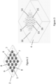
- Figure 1 shows a superconducting quantum computing circuit package 1 according to an embodiment of the present invention.
- the package 1 includes a substrate 2, a holder 3 for the substrate 2 and a cover 4.
- the package 1 is shown in Figure 1 in an expanded configuration, e.g. prior to assembly.
- Figure 2 shows the substrate 2 of the superconducting quantum computing circuit package 1 shown in Figure 1 .
- the substrate is typically made from silicon or sapphire.
- a quantum computing circuit 5 is formed on the surface of the substrate 2 (a similar circuit may also be formed on the opposite face of the substrate 2).
- the quantum computing circuit 5 includes multiple qubits 6 arranged in a regular geometric grid.
- the qubits 6 are connected together by respective interconnections 7.
- the qubits 6 are addressed by respective control lines and readout elements, e.g. as disclosed in the Applicant's previous application published as WO 2017/021714 A1 .
- Multiple holes 8 are formed (e.g. machined) through the thickness of the substrate 2.
- the holes 8 are arranged in a regular geometric grid to intersperse the qubits 6. (Similarly, on the reverse of the substrate 2, the qubits and their interconnections will be formed between the holes 8.)
- the upper surface 9 of the holder 3 has a recess 10 formed in the surface 9 such that a rim 11 extends around the perimeter of the upper surface 9.
- the depth of the recess 10 is substantially equal to the thickness of the substrate 2, so that when the substrate 2 is placed onto the upper surface 9 of the holder 3, the upper face of the substrate 2 lies flush with the rim 11 of the holder 3.
- the projections 12 are formed on the upper surface 9 of the holder 3 in the recess 10.
- the projections 12 correspond in position and number to the holes 8 formed through the substrate 2.
- the projections 12 have a cylindrical diameter slightly smaller than the corresponding diameter of the holes 8 in the substrate 2, and a height that is slightly greater than the thickness of the substrate 2, such that when the substrate 2 is placed onto the upper surface 9 of the holder 3 and the cover 4 is placed on top of the holder 3 to enclose the substrate 2, the projections 12 pass through the corresponding holes 8 and the top of the projections 12 contact the inner surface of the cover 4.
- Multiple apertures 13 are formed through the holder 3 within the recess 10.
- multiple apertures 14 are formed through the cover 4.
- the apertures 13, 14 through the holder 3 and the cover 4 correspond in number and position to the qubits 6 formed on the substrate 2.
- the apertures 13, 14 allow off-chip control wiring to be routed through the holder 3 and the cover 4 to connect to the qubits 6 of the quantum computing circuit 5.
- Figure 3 shows the underside of the cover 4.
- the apertures 14 through the cover 4 can be seen, as can cut-out channels 15 that extend between the apertures 14.
- the cut-out channels 15 correspond in position and number to the interconnections 7 between the qubits 6 of the quantum computing circuit 5.
- the width of the cut-out channels 15 is wider than the width of the interconnections 7, such that when the cover 4 is placed on top of the substrate 2, the cover 4 does not come into contact with (and therefore does not short-circuit) the circuit elements of the quantum computing circuit 5. (When a quantum computing circuit is formed on the opposite face of the substrate 2, similar cut-out channels may be provided between the apertures 13 formed through the holder 3.)
- the underside of the cover 4 shown in Figure 3 also shows multiple depressions 16 formed in the underside of the cover 4.
- the depressions 16 correspond in position and number to the holes 8 formed through the substrate 2, and thus also to the projections 12 of the holder 3.
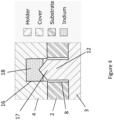
- Figure 4 shows the cross-section of part of the superconducting quantum computing circuit package 1.
- Figure 4 shows the holder 3, cover 4 and the substrate 2 around a depression 16 in the cover 4, a hole 8 in the substrate 2 and a projection 12 of the holder 3.
- the projection 12 has a tapered distal end 17 which passes through the hole 8 in the substrate 2 and is aligned with the depression 16 in the cover 4.
- the depression 16 (and all the other depressions 16 in the cover 4) has a cylindrical diameter slightly larger than the corresponding diameter of the projection 12, such that the projection 12 is received by the depression 16.
- the depression 16 (and all the other depressions 16 in the cover 4) is nearly filled with a volume of indium 18.
- the indium 18 is a soft metal that deforms when the substrate 2 is sandwiched between the cover 4 and the holder 3, such that the tapered distal end 17 of the projection 12 protrudes into the volume of indium 18.
- Figure 7 shows the effect on the suppression of electromagnetic modes in the operational frequency range of the quantum computing circuit, owing to the uplift in the frequency of lowest frequency spurious mode, when using a superconducting quantum computing circuit package according to an embodiment of the present invention.
Landscapes
- Engineering & Computer Science (AREA)
- General Physics & Mathematics (AREA)
- Theoretical Computer Science (AREA)
- Physics & Mathematics (AREA)
- Mathematical Analysis (AREA)
- Computing Systems (AREA)
- Evolutionary Computation (AREA)
- Condensed Matter Physics & Semiconductors (AREA)
- Computational Mathematics (AREA)
- Mathematical Optimization (AREA)
- Pure & Applied Mathematics (AREA)
- Data Mining & Analysis (AREA)
- General Engineering & Computer Science (AREA)
- Mathematical Physics (AREA)
- Software Systems (AREA)
- Artificial Intelligence (AREA)
- Superconductor Devices And Manufacturing Methods Thereof (AREA)
- Containers, Films, And Cooling For Superconductive Devices (AREA)
Claims (14)
- Supraleitendes Quantenrechenschaltungspaket (1), umfassend:ein Substrat (2), auf dem eine supraleitende Quantenrechenschaltung (5) ausgebildet ist, wobei die supraleitende Quantenrechenschaltung eine Vielzahl von Schaltungselementen umfasst und das Substrat (2) ein oder mehrere Löcher (8) umfasst, die zwischen der Vielzahl von Schaltungselementen angeordnet sind, wobei sich das eine oder die mehreren Löcher (8) durch eine Dicke des Substrats (2) erstrecken; undeinen Halter (3), der eine Oberfläche umfasst, auf der das Substrat (2) aufgenommen ist, und eine Abdeckung (4), die auf einer dem Halter (3) gegenüberliegenden Seite des Substrats (2) angeordnet ist, wobei der Halter (3) einen oder mehrere Vorsprünge (12) umfasst, die auf der Oberfläche angeordnet sind und von dieser vorspringen;wobei der eine oder die mehreren Vorsprünge (12) durch das eine oder die mehreren Löcher (8) im Substrat (2) vorragen und die Abdeckung (4) kontaktieren, um elektromagnetische Moden im Betriebsfrequenzbereich der Quantenrechenschaltung zu unterdrücken; undwobei der Halter (3) und die Abdeckung (4) aus einem Metall und/oder einem Supraleiter ausgebildet sind;dadurch gekennzeichnet, dass:
der Halter (3) eine oder mehrere Öffnungen (13) umfasst, die durch die Oberfläche des Halters hindurch ausgebildet sind und/oder die Abdeckung (4) eine oder mehrere Öffnungen (14) umfasst, die durch die Abdeckung hindurch ausgebildet sind;
wobei das supraleitende Quantenrechenschaltungspaket einen oder mehrere Drähte umfasst, die so angeordnet sind, dass sie durch die eine beziehungsweise die mehreren Öffnungen (13, 14) verlaufen, um eine Verbindung mit der Quantenrechenschaltung (5) herzustellen. - Supraleitendes Quantenrechenschaltungspaket (1) nach Anspruch 1, wobei die Vielzahl von Schaltungselementen eines oder mehrere umfassen von: einem oder mehreren Qubits (6), einer oder mehreren Steuerleitungen und einem oder mehreren Ausleseelementen.
- Supraleitendes Quantenrechenschaltungspaket (1) nach Anspruch 2, wobei der maximale Abstand zwischen benachbarten Löchern (8) im Substrat und/oder zwischen benachbarten Vorsprüngen (12) auf dem Halter (3) einer chipähnlichen Mode entspricht, die eine höhere Frequenz als die maximale Betriebsfrequenz der Quantenrechenschaltung aufweist.
- Supraleitendes Quantenrechenschaltungspaket (1) nach Anspruch 2 oder 3, wobei die Vielzahl von Schaltungselementen mindestens zwei Qubits (6) umfasst, wobei das eine oder die mehreren Löcher (8) derart zwischen den mindestens zwei Qubits (6) angeordnet sind, dass der eine oder die mehreren Vorsprünge (12) so angeordnet sind, dass sie zwischen benachbarten Qubits (6) verlaufen.
- Supraleitendes Quantenrechenschaltungspaket (1) nach einem der vorstehenden Ansprüche, wobei die Oberfläche zum Aufnehmen des Substrats (2) von einer Fläche des Halters (3) vertieft ist.
- Supraleitendes Quantenrechenschaltungspaket (1) nach Anspruch 5, wobei die Oberfläche von der Fläche des Halters (3) um eine Tiefe vertieft ist, die im Wesentlichen gleich der Dicke des Substrats (2) und/oder der Höhe des einen oder der mehreren Vorsprünge (12) ist.
- Supraleitendes Quantenrechenschaltungspaket (1) nach einem der vorstehenden Ansprüche, wobei das eine oder die mehreren Löcher (8) in Form und Größe dem einen oder den mehreren Vorsprüngen (12) derart entsprechen, dass das eine oder die mehreren Löcher (8) den einen oder die mehreren entsprechenden Vorsprünge (12) aufnehmen, wenn sich das Substrat (2) auf dem Halter (3) befindet.
- Supraleitendes Quantenrechenschaltungspaket (1) nach einem der vorstehenden Ansprüche, wobei der eine oder die mehreren Vorsprünge (12) eine Höhe aufweisen, die größer oder gleich der halben Dicke des Substrats (2) ist.
- Supraleitendes Quantenrechenschaltungspaket (1) nach einem der vorstehenden Ansprüche, wobei der eine oder die mehreren Vorsprünge (12), die in das eine oder die mehreren Löcher (8) im Substrat vorragen, so angeordnet sind, dass sie elektromagnetische Moden unterdrücken, die eine Frequenz von kleiner als 20 GHz, z.B. kleiner als 15 GHz, z.B. kleiner als 12 GHz, aufweisen.
- Supraleitendes Quantenrechenschaltungspaket (1) nach einem der vorstehenden Ansprüche, wobei Abdeckung (4) von der Vielzahl von Schaltungselementen auf dem Substrat (2) beabstandet ist.
- Supraleitendes Quantenrechenschaltungspaket (1) nach einem der vorstehenden Ansprüche, wobei die Abdeckung (4) in ihrer Oberfläche Aussparungen umfasst, die der Vielzahl von Schaltungselementen auf dem Substrat (2) entsprechen und diesen zugewandt sind.
- Supraleitendes Quantenrechenschaltungspaket nach einem der vorstehenden Ansprüche, wobei der Halter (3) und die Abdeckung (4) einer Oberflächenbehandlung unterzogen wurden.
- Supraleitendes Quantenrechenschaltungspaket (1) nach einem der vorstehenden Ansprüche, wobei die Abdeckung (4) eine oder mehrere Einsenkungen (16) umfasst, die dem einen oder den mehreren Vorsprüngen (12) entsprechen, wobei die eine oder die mehreren Einsenkungen (16) so angeordnet sind, dass sie den einen oder die mehreren Vorsprünge (12) derart aufnehmen, dass der eine oder die mehreren Vorsprünge (12) die Abdeckung (4) in der einen oder den mehreren entsprechenden Einsenkungen (16) kontaktieren.
- Supraleitendes Quantenrechenschaltungspaket (1) nach Anspruch 13, wobei die Abdeckung (4) ein Volumen aus einem leitfähigen Material in der einen oder den mehreren Einsenkungen (16) umfasst, wobei das Material weicher ist als das Metall der Abdeckung (4).
Applications Claiming Priority (2)
| Application Number | Priority Date | Filing Date | Title |
|---|---|---|---|
| GBGB1813188.8A GB201813188D0 (en) | 2018-08-13 | 2018-08-13 | Superconducting quantum computing circuit package |
| PCT/GB2019/052271 WO2020035672A1 (en) | 2018-08-13 | 2019-08-13 | Superconducting quantum computing circuit package |
Publications (3)
| Publication Number | Publication Date |
|---|---|
| EP3837720A1 EP3837720A1 (de) | 2021-06-23 |
| EP3837720C0 EP3837720C0 (de) | 2024-09-18 |
| EP3837720B1 true EP3837720B1 (de) | 2024-09-18 |
Family
ID=63667187
Family Applications (1)
| Application Number | Title | Priority Date | Filing Date |
|---|---|---|---|
| EP19758454.3A Active EP3837720B1 (de) | 2018-08-13 | 2019-08-13 | Supraleitendes quantenrechenschaltungspaket |
Country Status (8)
| Country | Link |
|---|---|
| US (1) | US11937517B2 (de) |
| EP (1) | EP3837720B1 (de) |
| JP (2) | JP7402859B2 (de) |
| KR (1) | KR102929492B1 (de) |
| CN (2) | CN120187270A (de) |
| ES (1) | ES2989198T3 (de) |
| GB (1) | GB201813188D0 (de) |
| WO (1) | WO2020035672A1 (de) |
Families Citing this family (7)
| Publication number | Priority date | Publication date | Assignee | Title |
|---|---|---|---|---|
| GB201813188D0 (en) * | 2018-08-13 | 2018-09-26 | Univ Oxford Innovation Ltd | Superconducting quantum computing circuit package |
| CN111260067B (zh) * | 2020-01-15 | 2023-04-18 | 中国科学技术大学 | 量子处理电路结构及提高谐振频率的方法 |
| JP7456304B2 (ja) * | 2020-06-19 | 2024-03-27 | 日本電気株式会社 | 量子デバイス |
| JP7567222B2 (ja) * | 2020-06-19 | 2024-10-16 | 日本電気株式会社 | 量子デバイス |
| JP7732250B2 (ja) | 2021-07-09 | 2025-09-02 | 日本電気株式会社 | 量子デバイス |
| CN115204402B (zh) * | 2022-06-24 | 2025-04-11 | 深圳国际量子研究院 | 一种超导量子芯片连接结构及连接方法 |
| JPWO2024185131A1 (de) | 2023-03-09 | 2024-09-12 |
Family Cites Families (16)
| Publication number | Priority date | Publication date | Assignee | Title |
|---|---|---|---|---|
| JP3129288B2 (ja) * | 1998-05-28 | 2001-01-29 | 日本電気株式会社 | マイクロ波集積回路マルチチップモジュール、マイクロ波集積回路マルチチップモジュールの実装構造 |
| JP6360499B2 (ja) | 2013-01-18 | 2018-07-18 | イェール ユニバーシティーYale University | 少なくとも1つの囲いを有する超伝導デバイスを製造するための方法 |
| US9219298B2 (en) | 2013-03-15 | 2015-12-22 | International Business Machines Corporation | Removal of spurious microwave modes via flip-chip crossover |
| US9520547B2 (en) | 2013-03-15 | 2016-12-13 | International Business Machines Corporation | Chip mode isolation and cross-talk reduction through buried metal layers and through-vias |
| WO2015178992A2 (en) * | 2014-02-28 | 2015-11-26 | Rigetti & Co., Inc. | Processing signals in a quantum computing system |
| US9836699B1 (en) * | 2015-04-27 | 2017-12-05 | Rigetti & Co. | Microwave integrated quantum circuits with interposer |
| US10068181B1 (en) * | 2015-04-27 | 2018-09-04 | Rigetti & Co, Inc. | Microwave integrated quantum circuits with cap wafer and methods for making the same |
| US9524470B1 (en) * | 2015-06-12 | 2016-12-20 | International Business Machines Corporation | Modular array of vertically integrated superconducting qubit devices for scalable quantum computing |
| US9985193B2 (en) * | 2015-06-30 | 2018-05-29 | International Business Machines Corporation | Architecture for coupling quantum bits using localized resonators |
| GB201513774D0 (en) * | 2015-08-04 | 2015-09-16 | Isis Innovation | Quantum information processing system |
| JP6581545B2 (ja) * | 2016-07-15 | 2019-09-25 | 株式会社東芝 | 計算装置 |
| US11569428B2 (en) * | 2016-12-27 | 2023-01-31 | Santa Clara | Superconducting qubit device packages |
| CN107564868B (zh) | 2017-07-07 | 2019-08-02 | 清华大学 | 一种超导量子计算芯片的集成封装结构和方法 |
| RU177295U1 (ru) | 2017-09-12 | 2018-02-15 | Федеральное государственное бюджетное образовательное учреждение высшего образования "Московский технологический университет" (МИРЭА) | Флаксонный кольцевой детектор |
| GB201813188D0 (en) * | 2018-08-13 | 2018-09-26 | Univ Oxford Innovation Ltd | Superconducting quantum computing circuit package |
| RU2716028C1 (ru) | 2018-12-26 | 2020-03-05 | Кавокин Алексий Витальевич | Способ формирования кубита |
-
2018
- 2018-08-13 GB GBGB1813188.8A patent/GB201813188D0/en not_active Ceased
-
2019
- 2019-08-13 EP EP19758454.3A patent/EP3837720B1/de active Active
- 2019-08-13 KR KR1020217007601A patent/KR102929492B1/ko active Active
- 2019-08-13 CN CN202510209246.8A patent/CN120187270A/zh active Pending
- 2019-08-13 WO PCT/GB2019/052271 patent/WO2020035672A1/en not_active Ceased
- 2019-08-13 US US17/267,057 patent/US11937517B2/en active Active
- 2019-08-13 ES ES19758454T patent/ES2989198T3/es active Active
- 2019-08-13 JP JP2021507577A patent/JP7402859B2/ja active Active
- 2019-08-13 CN CN201980053413.7A patent/CN112567524B/zh active Active
-
2023
- 2023-12-11 JP JP2023208685A patent/JP7719161B2/ja active Active
Also Published As
| Publication number | Publication date |
|---|---|
| WO2020035672A1 (en) | 2020-02-20 |
| US11937517B2 (en) | 2024-03-19 |
| JP2021534583A (ja) | 2021-12-09 |
| EP3837720C0 (de) | 2024-09-18 |
| GB201813188D0 (en) | 2018-09-26 |
| CN120187270A (zh) | 2025-06-20 |
| EP3837720A1 (de) | 2021-06-23 |
| ES2989198T3 (es) | 2024-11-25 |
| KR20210068405A (ko) | 2021-06-09 |
| CN112567524A (zh) | 2021-03-26 |
| JP7402859B2 (ja) | 2023-12-21 |
| JP2024037840A (ja) | 2024-03-19 |
| US20210296559A1 (en) | 2021-09-23 |
| JP7719161B2 (ja) | 2025-08-05 |
| CN112567524B (zh) | 2025-03-18 |
| KR102929492B1 (ko) | 2026-02-20 |
Similar Documents
| Publication | Publication Date | Title |
|---|---|---|
| EP3837720B1 (de) | Supraleitendes quantenrechenschaltungspaket | |
| US10897808B2 (en) | Filter device and plasma processing apparatus | |
| US7612638B2 (en) | Waveguides in integrated circuits | |
| US20060237819A1 (en) | Semiconductor device | |
| US11917750B2 (en) | Shielding structure for system-in-package and electronic device | |
| US10438862B2 (en) | Electromagnetic shield structure of high frequency circuit and high frequency module | |
| US6011299A (en) | Apparatus to minimize integrated circuit heatsink E.M.I. radiation | |
| US6583987B2 (en) | Electromagnetic interference and heatsinking | |
| KR20100054079A (ko) | 반도체 집적회로 칩, 적층형 칩 커패시터 및 반도체 집적회로 칩 패키지 | |
| US20120074559A1 (en) | Integrated circuit package using through substrate vias to ground lid | |
| US9036364B1 (en) | Circuit board with signal layers of different dimensions to communicate signals of different frequencies | |
| HK40045168B (en) | Superconducting quantum computing circuit package | |
| HK40045168A (en) | Superconducting quantum computing circuit package | |
| JP7621004B2 (ja) | 基板を通る接続部を有する3dイオントラップ | |
| US8728874B2 (en) | Method and apparatus for low inductive design pattern | |
| HK40127053A (zh) | 超导量子计算电路封装 | |
| RU2799343C2 (ru) | Модуль сверхпроводниковой схемы для квантовых вычислений | |
| US20240040687A1 (en) | Circuit board assembly | |
| US20230145380A1 (en) | Waveguide package, method of manufacturing the same, and package housing | |
| US20080035369A1 (en) | Shielded circuit board and method for shielding a circuit board | |
| US20170141047A1 (en) | Microwave and millimeter wave package | |
| CN112292916B (zh) | 一种集成电路 | |
| JP2016171157A (ja) | 高周波半導体用パッケージ | |
| JP2016111196A (ja) | 超伝導高周波装置 | |
| US20220248541A1 (en) | System in package (sip) socket connector interface |
Legal Events
| Date | Code | Title | Description |
|---|---|---|---|
| STAA | Information on the status of an ep patent application or granted ep patent |
Free format text: STATUS: UNKNOWN |
|
| STAA | Information on the status of an ep patent application or granted ep patent |
Free format text: STATUS: THE INTERNATIONAL PUBLICATION HAS BEEN MADE |
|
| PUAI | Public reference made under article 153(3) epc to a published international application that has entered the european phase |
Free format text: ORIGINAL CODE: 0009012 |
|
| STAA | Information on the status of an ep patent application or granted ep patent |
Free format text: STATUS: REQUEST FOR EXAMINATION WAS MADE |
|
| 17P | Request for examination filed |
Effective date: 20210126 |
|
| AK | Designated contracting states |
Kind code of ref document: A1 Designated state(s): AL AT BE BG CH CY CZ DE DK EE ES FI FR GB GR HR HU IE IS IT LI LT LU LV MC MK MT NL NO PL PT RO RS SE SI SK SM TR |
|
| REG | Reference to a national code |
Ref country code: HK Ref legal event code: DE Ref document number: 40045168 Country of ref document: HK |
|
| DAV | Request for validation of the european patent (deleted) | ||
| DAX | Request for extension of the european patent (deleted) | ||
| STAA | Information on the status of an ep patent application or granted ep patent |
Free format text: STATUS: EXAMINATION IS IN PROGRESS |
|
| 17Q | First examination report despatched |
Effective date: 20230901 |
|
| REG | Reference to a national code |
Ref country code: DE Ref legal event code: R079 Free format text: PREVIOUS MAIN CLASS: H01L0027180000 Ipc: H10N0069000000 Ref document number: 602019059106 Country of ref document: DE |
|
| RIC1 | Information provided on ipc code assigned before grant |
Ipc: G06N 10/40 20220101ALI20240222BHEP Ipc: H10N 60/81 20230101ALI20240222BHEP Ipc: H10N 69/00 20230101AFI20240222BHEP |
|
| GRAP | Despatch of communication of intention to grant a patent |
Free format text: ORIGINAL CODE: EPIDOSNIGR1 |
|
| STAA | Information on the status of an ep patent application or granted ep patent |
Free format text: STATUS: GRANT OF PATENT IS INTENDED |
|
| INTG | Intention to grant announced |
Effective date: 20240403 |
|
| GRAS | Grant fee paid |
Free format text: ORIGINAL CODE: EPIDOSNIGR3 |
|
| GRAA | (expected) grant |
Free format text: ORIGINAL CODE: 0009210 |
|
| STAA | Information on the status of an ep patent application or granted ep patent |
Free format text: STATUS: THE PATENT HAS BEEN GRANTED |
|
| AK | Designated contracting states |
Kind code of ref document: B1 Designated state(s): AL AT BE BG CH CY CZ DE DK EE ES FI FR GB GR HR HU IE IS IT LI LT LU LV MC MK MT NL NO PL PT RO RS SE SI SK SM TR |
|
| REG | Reference to a national code |
Ref country code: GB Ref legal event code: FG4D |
|
| REG | Reference to a national code |
Ref country code: CH Ref legal event code: EP |
|
| REG | Reference to a national code |
Ref country code: IE Ref legal event code: FG4D |
|
| REG | Reference to a national code |
Ref country code: DE Ref legal event code: R096 Ref document number: 602019059106 Country of ref document: DE |
|
| U01 | Request for unitary effect filed |
Effective date: 20240918 |
|
| U07 | Unitary effect registered |
Designated state(s): AT BE BG DE DK EE FI FR IT LT LU LV MT NL PT RO SE SI Effective date: 20241009 |
|
| REG | Reference to a national code |
Ref country code: ES Ref legal event code: FG2A Ref document number: 2989198 Country of ref document: ES Kind code of ref document: T3 Effective date: 20241125 |
|
| PG25 | Lapsed in a contracting state [announced via postgrant information from national office to epo] |
Ref country code: NO Free format text: LAPSE BECAUSE OF FAILURE TO SUBMIT A TRANSLATION OF THE DESCRIPTION OR TO PAY THE FEE WITHIN THE PRESCRIBED TIME-LIMIT Effective date: 20241218 |
|
| PG25 | Lapsed in a contracting state [announced via postgrant information from national office to epo] |
Ref country code: GR Free format text: LAPSE BECAUSE OF FAILURE TO SUBMIT A TRANSLATION OF THE DESCRIPTION OR TO PAY THE FEE WITHIN THE PRESCRIBED TIME-LIMIT Effective date: 20241219 |
|
| PG25 | Lapsed in a contracting state [announced via postgrant information from national office to epo] |
Ref country code: HR Free format text: LAPSE BECAUSE OF FAILURE TO SUBMIT A TRANSLATION OF THE DESCRIPTION OR TO PAY THE FEE WITHIN THE PRESCRIBED TIME-LIMIT Effective date: 20240918 |
|
| PG25 | Lapsed in a contracting state [announced via postgrant information from national office to epo] |
Ref country code: RS Free format text: LAPSE BECAUSE OF FAILURE TO SUBMIT A TRANSLATION OF THE DESCRIPTION OR TO PAY THE FEE WITHIN THE PRESCRIBED TIME-LIMIT Effective date: 20241218 |
|
| PG25 | Lapsed in a contracting state [announced via postgrant information from national office to epo] |
Ref country code: RS Free format text: LAPSE BECAUSE OF FAILURE TO SUBMIT A TRANSLATION OF THE DESCRIPTION OR TO PAY THE FEE WITHIN THE PRESCRIBED TIME-LIMIT Effective date: 20241218 Ref country code: NO Free format text: LAPSE BECAUSE OF FAILURE TO SUBMIT A TRANSLATION OF THE DESCRIPTION OR TO PAY THE FEE WITHIN THE PRESCRIBED TIME-LIMIT Effective date: 20241218 Ref country code: HR Free format text: LAPSE BECAUSE OF FAILURE TO SUBMIT A TRANSLATION OF THE DESCRIPTION OR TO PAY THE FEE WITHIN THE PRESCRIBED TIME-LIMIT Effective date: 20240918 Ref country code: GR Free format text: LAPSE BECAUSE OF FAILURE TO SUBMIT A TRANSLATION OF THE DESCRIPTION OR TO PAY THE FEE WITHIN THE PRESCRIBED TIME-LIMIT Effective date: 20241219 |
|
| PG25 | Lapsed in a contracting state [announced via postgrant information from national office to epo] |
Ref country code: IS Free format text: LAPSE BECAUSE OF FAILURE TO SUBMIT A TRANSLATION OF THE DESCRIPTION OR TO PAY THE FEE WITHIN THE PRESCRIBED TIME-LIMIT Effective date: 20250118 |
|
| PG25 | Lapsed in a contracting state [announced via postgrant information from national office to epo] |
Ref country code: SM Free format text: LAPSE BECAUSE OF FAILURE TO SUBMIT A TRANSLATION OF THE DESCRIPTION OR TO PAY THE FEE WITHIN THE PRESCRIBED TIME-LIMIT Effective date: 20240918 |
|
| PG25 | Lapsed in a contracting state [announced via postgrant information from national office to epo] |
Ref country code: PL Free format text: LAPSE BECAUSE OF FAILURE TO SUBMIT A TRANSLATION OF THE DESCRIPTION OR TO PAY THE FEE WITHIN THE PRESCRIBED TIME-LIMIT Effective date: 20240918 Ref country code: CZ Free format text: LAPSE BECAUSE OF FAILURE TO SUBMIT A TRANSLATION OF THE DESCRIPTION OR TO PAY THE FEE WITHIN THE PRESCRIBED TIME-LIMIT Effective date: 20240918 |
|
| PG25 | Lapsed in a contracting state [announced via postgrant information from national office to epo] |
Ref country code: SK Free format text: LAPSE BECAUSE OF FAILURE TO SUBMIT A TRANSLATION OF THE DESCRIPTION OR TO PAY THE FEE WITHIN THE PRESCRIBED TIME-LIMIT Effective date: 20240918 |
|
| PLBE | No opposition filed within time limit |
Free format text: ORIGINAL CODE: 0009261 |
|
| STAA | Information on the status of an ep patent application or granted ep patent |
Free format text: STATUS: NO OPPOSITION FILED WITHIN TIME LIMIT |
|
| 26N | No opposition filed |
Effective date: 20250619 |
|
| U20 | Renewal fee for the european patent with unitary effect paid |
Year of fee payment: 7 Effective date: 20250828 |
|
| PGFP | Annual fee paid to national office [announced via postgrant information from national office to epo] |
Ref country code: ES Payment date: 20250918 Year of fee payment: 7 |
|
| PGFP | Annual fee paid to national office [announced via postgrant information from national office to epo] |
Ref country code: GB Payment date: 20250922 Year of fee payment: 7 |
|
| PGFP | Annual fee paid to national office [announced via postgrant information from national office to epo] |
Ref country code: CH Payment date: 20250901 Year of fee payment: 7 |
|
| PG25 | Lapsed in a contracting state [announced via postgrant information from national office to epo] |
Ref country code: MC Free format text: LAPSE BECAUSE OF FAILURE TO SUBMIT A TRANSLATION OF THE DESCRIPTION OR TO PAY THE FEE WITHIN THE PRESCRIBED TIME-LIMIT Effective date: 20240918 |