EP3835768B1 - Method for improving kikuchi diffraction patterns - Google Patents
Method for improving kikuchi diffraction patterns Download PDFInfo
- Publication number
- EP3835768B1 EP3835768B1 EP19216196.6A EP19216196A EP3835768B1 EP 3835768 B1 EP3835768 B1 EP 3835768B1 EP 19216196 A EP19216196 A EP 19216196A EP 3835768 B1 EP3835768 B1 EP 3835768B1
- Authority
- EP
- European Patent Office
- Prior art keywords
- tkd
- pattern
- sample
- electron
- diffraction
- Prior art date
- Legal status (The legal status is an assumption and is not a legal conclusion. Google has not performed a legal analysis and makes no representation as to the accuracy of the status listed.)
- Active
Links
- 238000000034 method Methods 0.000 title claims description 59
- 238000005259 measurement Methods 0.000 claims description 31
- 230000014509 gene expression Effects 0.000 claims description 29
- 238000010894 electron beam technology Methods 0.000 claims description 25
- 239000013078 crystal Substances 0.000 claims description 21
- 238000013507 mapping Methods 0.000 claims description 16
- 230000005540 biological transmission Effects 0.000 claims description 12
- 230000008602 contraction Effects 0.000 claims description 8
- 238000004590 computer program Methods 0.000 claims description 4
- 238000002149 energy-dispersive X-ray emission spectroscopy Methods 0.000 description 22
- 238000001887 electron backscatter diffraction Methods 0.000 description 13
- OAICVXFJPJFONN-UHFFFAOYSA-N Phosphorus Chemical compound [P] OAICVXFJPJFONN-UHFFFAOYSA-N 0.000 description 7
- 230000000694 effects Effects 0.000 description 5
- 238000003384 imaging method Methods 0.000 description 5
- 230000033001 locomotion Effects 0.000 description 5
- 239000000463 material Substances 0.000 description 5
- 239000000203 mixture Substances 0.000 description 4
- 238000004458 analytical method Methods 0.000 description 3
- 230000001419 dependent effect Effects 0.000 description 3
- 239000002178 crystalline material Substances 0.000 description 2
- 238000013459 approach Methods 0.000 description 1
- 238000001816 cooling Methods 0.000 description 1
- 238000012937 correction Methods 0.000 description 1
- 238000009795 derivation Methods 0.000 description 1
- 238000001514 detection method Methods 0.000 description 1
- 238000011161 development Methods 0.000 description 1
- 230000018109 developmental process Effects 0.000 description 1
- 238000002524 electron diffraction data Methods 0.000 description 1
- 238000001493 electron microscopy Methods 0.000 description 1
- 238000000724 energy-dispersive X-ray spectrum Methods 0.000 description 1
- 230000001771 impaired effect Effects 0.000 description 1
- 230000000737 periodic effect Effects 0.000 description 1
- 238000012545 processing Methods 0.000 description 1
- 230000008707 rearrangement Effects 0.000 description 1
- 238000012552 review Methods 0.000 description 1
- 238000011144 upstream manufacturing Methods 0.000 description 1
Images
Classifications
-
- G—PHYSICS
- G01—MEASURING; TESTING
- G01N—INVESTIGATING OR ANALYSING MATERIALS BY DETERMINING THEIR CHEMICAL OR PHYSICAL PROPERTIES
- G01N23/00—Investigating or analysing materials by the use of wave or particle radiation, e.g. X-rays or neutrons, not covered by groups G01N3/00 – G01N17/00, G01N21/00 or G01N22/00
- G01N23/20—Investigating or analysing materials by the use of wave or particle radiation, e.g. X-rays or neutrons, not covered by groups G01N3/00 – G01N17/00, G01N21/00 or G01N22/00 by using diffraction of the radiation by the materials, e.g. for investigating crystal structure; by using scattering of the radiation by the materials, e.g. for investigating non-crystalline materials; by using reflection of the radiation by the materials
- G01N23/20058—Measuring diffraction of electrons, e.g. low energy electron diffraction [LEED] method or reflection high energy electron diffraction [RHEED] method
-
- H—ELECTRICITY
- H01—ELECTRIC ELEMENTS
- H01J—ELECTRIC DISCHARGE TUBES OR DISCHARGE LAMPS
- H01J37/00—Discharge tubes with provision for introducing objects or material to be exposed to the discharge, e.g. for the purpose of examination or processing thereof
- H01J37/02—Details
- H01J37/244—Detectors; Associated components or circuits therefor
-
- G—PHYSICS
- G01—MEASURING; TESTING
- G01N—INVESTIGATING OR ANALYSING MATERIALS BY DETERMINING THEIR CHEMICAL OR PHYSICAL PROPERTIES
- G01N23/00—Investigating or analysing materials by the use of wave or particle radiation, e.g. X-rays or neutrons, not covered by groups G01N3/00 – G01N17/00, G01N21/00 or G01N22/00
- G01N23/20—Investigating or analysing materials by the use of wave or particle radiation, e.g. X-rays or neutrons, not covered by groups G01N3/00 – G01N17/00, G01N21/00 or G01N22/00 by using diffraction of the radiation by the materials, e.g. for investigating crystal structure; by using scattering of the radiation by the materials, e.g. for investigating non-crystalline materials; by using reflection of the radiation by the materials
- G01N23/2055—Analysing diffraction patterns
-
- H—ELECTRICITY
- H01—ELECTRIC ELEMENTS
- H01J—ELECTRIC DISCHARGE TUBES OR DISCHARGE LAMPS
- H01J37/00—Discharge tubes with provision for introducing objects or material to be exposed to the discharge, e.g. for the purpose of examination or processing thereof
- H01J37/02—Details
- H01J37/20—Means for supporting or positioning the object or the material; Means for adjusting diaphragms or lenses associated with the support
-
- G—PHYSICS
- G01—MEASURING; TESTING
- G01N—INVESTIGATING OR ANALYSING MATERIALS BY DETERMINING THEIR CHEMICAL OR PHYSICAL PROPERTIES
- G01N2223/00—Investigating materials by wave or particle radiation
- G01N2223/05—Investigating materials by wave or particle radiation by diffraction, scatter or reflection
- G01N2223/056—Investigating materials by wave or particle radiation by diffraction, scatter or reflection diffraction
- G01N2223/0565—Investigating materials by wave or particle radiation by diffraction, scatter or reflection diffraction diffraction of electrons, e.g. LEED
-
- G—PHYSICS
- G01—MEASURING; TESTING
- G01N—INVESTIGATING OR ANALYSING MATERIALS BY DETERMINING THEIR CHEMICAL OR PHYSICAL PROPERTIES
- G01N2223/00—Investigating materials by wave or particle radiation
- G01N2223/05—Investigating materials by wave or particle radiation by diffraction, scatter or reflection
- G01N2223/056—Investigating materials by wave or particle radiation by diffraction, scatter or reflection diffraction
- G01N2223/0566—Investigating materials by wave or particle radiation by diffraction, scatter or reflection diffraction analysing diffraction pattern
-
- G—PHYSICS
- G01—MEASURING; TESTING
- G01N—INVESTIGATING OR ANALYSING MATERIALS BY DETERMINING THEIR CHEMICAL OR PHYSICAL PROPERTIES
- G01N2223/00—Investigating materials by wave or particle radiation
- G01N2223/07—Investigating materials by wave or particle radiation secondary emission
- G01N2223/071—Investigating materials by wave or particle radiation secondary emission combination of measurements, at least 1 secondary emission
-
- G—PHYSICS
- G01—MEASURING; TESTING
- G01N—INVESTIGATING OR ANALYSING MATERIALS BY DETERMINING THEIR CHEMICAL OR PHYSICAL PROPERTIES
- G01N2223/00—Investigating materials by wave or particle radiation
- G01N2223/10—Different kinds of radiation or particles
- G01N2223/102—Different kinds of radiation or particles beta or electrons
-
- G—PHYSICS
- G01—MEASURING; TESTING
- G01N—INVESTIGATING OR ANALYSING MATERIALS BY DETERMINING THEIR CHEMICAL OR PHYSICAL PROPERTIES
- G01N2223/00—Investigating materials by wave or particle radiation
- G01N2223/40—Imaging
- G01N2223/401—Imaging image processing
-
- G—PHYSICS
- G01—MEASURING; TESTING
- G01N—INVESTIGATING OR ANALYSING MATERIALS BY DETERMINING THEIR CHEMICAL OR PHYSICAL PROPERTIES
- G01N2223/00—Investigating materials by wave or particle radiation
- G01N2223/60—Specific applications or type of materials
- G01N2223/605—Specific applications or type of materials phases
-
- G—PHYSICS
- G01—MEASURING; TESTING
- G01N—INVESTIGATING OR ANALYSING MATERIALS BY DETERMINING THEIR CHEMICAL OR PHYSICAL PROPERTIES
- G01N2223/00—Investigating materials by wave or particle radiation
- G01N2223/60—Specific applications or type of materials
- G01N2223/607—Specific applications or type of materials strain
-
- G—PHYSICS
- G01—MEASURING; TESTING
- G01N—INVESTIGATING OR ANALYSING MATERIALS BY DETERMINING THEIR CHEMICAL OR PHYSICAL PROPERTIES
- G01N23/00—Investigating or analysing materials by the use of wave or particle radiation, e.g. X-rays or neutrons, not covered by groups G01N3/00 – G01N17/00, G01N21/00 or G01N22/00
- G01N23/20—Investigating or analysing materials by the use of wave or particle radiation, e.g. X-rays or neutrons, not covered by groups G01N3/00 – G01N17/00, G01N21/00 or G01N22/00 by using diffraction of the radiation by the materials, e.g. for investigating crystal structure; by using scattering of the radiation by the materials, e.g. for investigating non-crystalline materials; by using reflection of the radiation by the materials
- G01N23/203—Measuring back scattering
-
- H—ELECTRICITY
- H01—ELECTRIC ELEMENTS
- H01J—ELECTRIC DISCHARGE TUBES OR DISCHARGE LAMPS
- H01J2237/00—Discharge tubes exposing object to beam, e.g. for analysis treatment, etching, imaging
- H01J2237/20—Positioning, supporting, modifying or maintaining the physical state of objects being observed or treated
- H01J2237/202—Movement
- H01J2237/20207—Tilt
Definitions
- the present invention refers to a method for improving the quality of a Kikuchi pattern obtained using a Transmission Kikuchi Diffraction, TKD, technique. Particularly, an influence of electron optics in an electron microscope used to obtain the TKD pattern shall be reduced.
- the present invention further relates to a measurement system for performing the method of the present invention as well as to a computer program for performing the method.
- EDS Energy dispersive spectroscopy
- EM electron microscopes
- SEM scanning electron microscopes
- the EDS detectors are often arranged upstream of the sample in the propagation direction of the electron beam.
- Kikuchi diffraction Another analytic technique for measuring crystal orientation that can be integrated into an electron microscope is Kikuchi diffraction.
- This technique can be implemented as electron backscatter diffraction (EBSD), which is also known as backscatter Kikuchi diffraction (BKD), or as transmission Kikuchi diffraction (TKD), also known as transmission electron backscatter diffraction (t-EBSD).
- EBSD electron backscatter diffraction
- BKD backscatter Kikuchi diffraction
- TKD transmission Kikuchi diffraction
- t-EBSD transmission electron backscatter diffraction
- backscatter electrons are detected from a direction perpendicular to the incident electron beam direction
- TKD transmitted and diffracted electrons are detected with a detector pointing in the direction of the incident beam.
- Both implementations can be theoretically applied to any crystalline material and provide the absolute crystal orientation and phase information with sub-micron spatial resolution.
- Kikuchi diffraction can be utilized to provide information on the phase of a sample-region of a crystalline material, particularly on the crystal structure, such as e.g., body-centered or face-centered cubic, orthorhombic or the like, and the spatial orientation of this crystal structure. Kikuchi diffraction can also reveal information on the strain in a material. In Kikuchi diffraction backscattered or transmitted electrons are diffracted by the periodic atomic lattice within the sample according to the Bragg condition before they exit the sample.
- TKD/EBSD At least part of the scattered electrons exit a sample with an angle-dependent intensity distribution. If this intensity distribution is detected using a two-dimensional detector, a Kikuchi pattern 20 as illustrated in Fig. 1 is recorded as a gnomonic projection on the detector surface. Therein, the position of the incident electron beam on the sample with respect to the detector surface is the so-called pattern center (PC).
- PC pattern center
- a typical feature of such Kikuchi patterns is the narrow Diffraction bands 21 with an angular width of two times the Bragg angle of the corresponding diffracting crystal planes. These bands can be considered to be formed by the Kossel cone of the respective crystal plane intersecting with the detector. With an appropriate experimental setup, the Diffraction bands can be approximated to be extending linearly on the detector.
- Such detected, linearly extending Diffraction bands can be related to an underlying crystal phase and orientation of the material within the source region. Theoretically, a minimum of three bands is necessary to determine the crystal orientation and phase represented by a given Kikuchi pattern. By individually indexing each band present in a Kikuchi pattern, the crystal phase and orientation at the source position can be unambiguously determined. By scanning a sample with an electron beam and obtaining a Kikuchi pattern for each point of such scanned sample grid, a TKD map can be obtained by analysing each individual pattern.
- an erroneous solution for crystal orientation and/or phase or no solution at all might be determined for a data point of the TKD map.
- the linear extension of a Kikuchi band may be impaired by at least one electronic optic within the electron microscope, particularly by a magnetic lens. Magnetic lenses are deliberately created in certain scanning electron microscopes with the aim to improve the scanning resolution of the electron beam. However, due to such magnetic lens, a residual magnetic field may exist in the SEM chamber that distorts the movements of the electrons. As a result, the electron diffraction patterns measured as TKD patterns can be distorted and comprise non-linear Diffraction bands as illustrated in Figure 2 .
- a first aspect of the present invention relates to a method of improving a Transmission Kikuchi Diffraction, TKD, pattern.
- the improvement particularly is that of unwarping a detected Kikuchi pattern in order to enable high precision indexing of the Kikuchi pattern.
- a TKD pattern of a sample is detected or determined based on detected signals corresponding to the TKD pattern.
- the TKD pattern is detected in an electron microscope that comprises at least one active electron lens that is configured for focussing an electron beam on a point on a sample.
- the electron microscope is a scanning electron microscope with an active scanning process.
- the sample is positioned in a distance D below the electron lens, particularly in a vertical distance D z .
- the detected TKD pattern is a two-dimensional map comprising a plurality of image points x D , y D , the index D referring throughout this document to the detected TKD pattern.
- the detected TKD pattern comprises at least one other value assigned to each of the plurality of image points, such as e.g., a greyscale value or the like.
- An example of a TKD pattern detected in the method of the invention is illustrated in Figure 2B .
- each of the image points x D , y D of the detected TKD pattern is mapped to a corresponding image point of an improved TKD pattern.
- the detected TKD pattern is mapped to an improved TKD pattern.
- the improved TKD pattern comprises a plurality of image points with the coordinates x 0 , y 0 .
- the amount of image points of the improved TKD pattern is preferably identical to the amount of image points of the detected TKD pattern.
- A, B, C, D denote trigonometric expressions that depend on the coordinates x 0 , y 0 and hence provide a relation between the image points coordinates x D , y D and x 0 , y 0 for each of the plurality of image points of the detected and improved TKD pattern.
- the inverse of the generalized terms is used.
- Z denotes an extension, i.e., a spatial extension, in the z-direction of a cylindrically symmetric magnetic field B Z of the electron lens.
- the magnetic field B Z is assumed as having a zero filed strength for any z > Z.
- the trigonometric expressions B and D define a rotation around a symmetry axis of the magnetic field B Z and the trigonometric expressions A and C define a combined rotation and contraction operation with respect to the symmetry axis of the magnetic field B Z .
- the improvement of the detected TKD pattern comprises the steps of rotating and/or rotating and contracting the detected TKD pattern, and each of the image points of the detected TKD pattern.
- each image point x 0 , y 0 of the improved TKD pattern is based on the coordinates of the corresponding image point x D , y D of the detected TKD pattern that is rotated and/or rotated and contracted to be mapped to the image point x 0 , y 0 of the improved TKD pattern.
- the method of the present invention hence allows to improve a TKD pattern, particularly to unwarp a TKD pattern by removing the influence of an electron lens magnetic field from the TKD pattern by using generalized terms that describe geometrical operations of rotation and/or rotation and contraction without considering an actual magnetic field in the electron microscope.
- the method of the invention provides sufficient results of improving a TKD pattern without knowing in detail the magnetic field within an electron microscope.
- the generalized terms are derived based on the geometry of the linear TKD setup in the microscope. In other words, using a linear setup for a TKD measurement allows for using the generalized terms.
- the improved TKD pattern is a TKD pattern for the electron microscope without being affected by active electron lens.
- the detected TKD pattern is a TKD pattern that is disturbed by a magnetic field present in the electron microscope due to the activity of the at least one electron lens and the improved TKD pattern is a TKD pattern that is not disturbed by a magnetic field present in the electron microscope due to the activity of the at least one electron lens.
- an actually detected TKD pattern is mapped to an improved TKD pattern via the generalized terms or the inverse thereof.
- the inverse of the generalized terms can be used to map the detected TKD pattern onto the improved TKD pattern.
- ⁇ denotes the circular frequency of the magnet-ic field B Z
- v z denotes the velocity of an electron in the z-direction of the electron beam.
- the prefactor ⁇ ⁇ D Z v is a parameter which is constant for a given measurement and which contains both the effect of the magnetic field and of the electron speed.
- the improvement of the TKD pattern depends on the distance of the image point to the symmetry axis of the magnetic field B Z , wherein the degree of rotation and/or rotation and contraction increases with the distance of the image point to the symmetry axis of field B Z .
- the method of the present invention further comprises the step of detecting a calibration TKD pattern of a calibration sample in the electron microscope without an active electron lens.
- the sample is also used as a calibration sample for calibrating the method of the invention.
- TKD patterns of further samples and/or further measurement points of the sample may be detected in the same electron microscope and subsequently improved by using the outcome of the calibration procedure.
- the calibration TKD pattern comprises a plurality of image points x C , y C and a plurality of mapping operations are performed on the detected TKD pattern, i.e., on each of the image points x D , y D using the generalized terms.
- each mapping operation is performed with a different set of values for y and ⁇ , i.e., with a different set of parameters ⁇ and ⁇ .
- an output TKD pattern resulting from the mapping operation is compared with the calibration TKD pattern and, based on such comparison, one set of values for y and ⁇ , i.e., one parameter set y and ⁇ , is determined.
- the so determined one set of values for y and ⁇ , i.e., the one parameter set y and ⁇ is then subsequently used for improving detected TKD patterns of the same electron microscope.
- the above step of comparison between the calibration TKD pattern with the output TKD pattern of each mapping operation is performed by image correlation of each of the output TKD pattern and the calibration TKD pattern.
- the patterns themselves are compared to each other by a pixel-based approach.
- Methods and algorithms for image correlation, particularly for providing a quantitative score as measure of image correlation are known to the person skilled in the art.
- the one parameter set is determined as that parameter set providing the highest degree of image correlation, e.g., providing the highest quantitative score for image correlation.
- the method of the invention further comprises the step of determining a plurality of diffraction bands from the detected Kikuchi pattern and from a calibration Kikuchi pattern.
- the diffraction bands are preferably determined using image processing algorithms which are state of the art.
- the diffraction bands are also preferably determined based on the greyscale values of the image points and a spatial cross-correlation for the greyscale values of neighboring image points.
- Diffraction bands can be advantageously used for the comparison between a calibration TKD pattern and the output TKD pattern of each mapping operation in determining the best set of values for ⁇ and ⁇ , i.e., the best set of parameter set ⁇ and ⁇ , as described above.
- a plurality of diffraction bands is determined from the detected diffraction pattern, wherein the diffraction bands comprise a plurality of image points x D DB , y D DB .
- a plurality of corresponding diffraction bands comprising a plurality of image points x 0 DB , y 0 DB is determined from the improved diffraction pattern.
- the diffraction bands and the corresponding diffraction bands are compared and one parameter set y and ⁇ providing the best match is determined based on the comparison.
- This parameter set is then preferably used for determining the improved TKD pattern.
- Diffraction bands are determined for each output TKD pattern, i.e., for each TKD pattern mapped from the detected TKD image with a certain defined parameter set. Further, straightness is determined for each of these Diffraction bands. In an undisturbed TKD pattern, the Diffraction bands should always be straight. Hence, any output TKD pattern with not straight Diffraction bands and the corresponding parameter set can be disregarded.
- the straightness of Diffraction bands i.e., a quantitative measure of such straightness
- the one parameter set is determined providing the output TKD pattern with the straightest Diffraction bands, i.e., the quantitative measure indicating the best straightness of Diffraction bands.
- crystal phase information are determined for each output TKD pattern based on the Diffraction bands determined for each of the output TKD pattern.
- crystal phase information refers to the type and orientation of a crystal lattice as it is can be determined based on a certain set of Diffraction bands.
- the one parameter set is determined that provides an output TKD pattern, the crystal phase information of which provide the best match with the crystal phase information determined based on the Diffraction bands of the calibration TKD pattern.
- a quantitative measure is preferably used for comparing the crystal phase information of the Diffraction bands of the output TKD patterns and the Diffraction bands of the calibration TKD pattern.
- the magnetic field i.e., the cylindrically symmetric magnetic field mentioned above
- B (0, 0, B Z )
- B Z the magnetic field
- the magnetic field i.e., the cylindrical symmetric magnetic field mentioned above
- the method of the invention is based on the assumption an artificial magnetic field with unrealistic properties, particularly the generalized terms are derived based on this assumption.
- the presumed magnetic field is assumed to be uniform, parallel to the z-axis and changing abruptly to zero at a certain distance from the sample. Such a magnetic field does not exist but only serves to motivate the form of the generalized terms. Hence, none of the parameters of the generalized terms has any physical meaning which would allow the description or representation of a real magnetic field, e.g., in the SEM. Further preferred, in the method of the invention it is presumed that Z ⁇ D Z , i.e., that the detecting device for the Kikuchi pattern (see below) is positioned in a field-free volume of the SEM chamber.
- the trigonometric expression A is of the form x 0 sin ⁇ ⁇ + y 0 1 ⁇ cos ⁇ ⁇
- the trigonometric expression B is of the form x 0 cos ⁇ + y 0 sin ⁇
- the trigonometric expression C is of the form ⁇ x 0 1 ⁇ cos ⁇ ⁇ + y 0 sin ⁇ ⁇
- the trigonometric expression D is of the form ⁇ x 0 sin ⁇ + y 0 cos ⁇ .
- the shift between a first improved image point with a first distance from the symmetry axis of a first improved TKD pattern and the corresponding first detected image point of a first detected TKD pattern will exceed the shift of a second improved image point with a second distance from the symmetry axis smaller than the first distance of a second improved TKD pattern and the corresponding second image point of the detected TKD pattern.
- Another aspect of the present invention refers to a measurement system comprising an electron microscope, EM, preferably a scanning electron microscope, SEM, with at least one electron lens, a TKD detector that is configured for detecting a TKD pattern of a sample positioned in distance D below the electron lens, and a control unit configured to perform the method for improving a Transmission Kikuchi Diffraction, TKD, pattern according to the invention as described above.
- the electron microscope preferably further comprises an EDS detector and is further configured for (scanning) electron microscopy/ imaging.
- the TKD detector is configured to perform TKD measurements under control of the control unit.
- the control unit that is further configured to control an electron source, the TKD detector and, eventually, the ESD detector.
- the electron lens is configured to focus an electron beam in a z-direction onto the sample.
- the (S)EM is configured to perform TKD measurements in the same configuration as used for with EDS measurements and/or as used for obtaining images with an imaging detector.
- the imaging detector is an in-column imaging detector that might be arranged inside a pole piece of an electron lens and/or between electron lenses of the column. In-column imaging detectors use secondary electrons (SE) and therefore may be named in-column SE detectors.
- the TKD detector comprises at least an active surface, e.g. phosphor screen for converting incident electrons to photons and a CCD or CMOS camera for obtaining image signals from these photons.
- the TKD detector comprises a cooling system and is configured for operating at room temperature for reducing the dark current of the CCD/CMOS camera.
- the TKD detector is a Bruker e-Flash EBSD detector retrofitted for optimal measurement geometry with a Bruker Optimus TKD measuring head used as a sample holder in the EM.
- first and second are used to describe various elements, these elements should not be limited by these terms. These terms are only used to distinguish one element from another element. For example, a first element may be named a second element and, similarly, a second element may be named a first element, without departing from the scope of the present invention. Expressions such as “at least one of,” when preceding a list of elements, modify the entire list of elements and do not modify the individual elements of the list. The term “substantially”, “about,” and similar terms are used as terms of approximation and not as terms of degree, and are intended to account for the inherent deviations in measured or calculated values that are recognized by those skilled in the art.
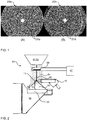
- Figure 1 illustrates the warping of a TKD pattern by a magnetic field of an electron lens.
- Figure 1A schematically illustrates a TKD pattern 20a that has been obtained in the absence of any magnetic field and hence comprises a plurality of straight Kikuchi lines 21a.
- the Kikuchi lines 21a have an angular width that corresponds to two times the Bragg angle of the corresponding crystal plane of the crystal lattice reflecting the electrons for producing that band 21.
- Figure 1B illustrates a TKD pattern 20b that was obtained in the same experimental setup and for the same measurement point of a sample in the presence of a magnetic field.
- the so obtained warped TKD pattern 20b comprises a plurality of bent (warped) Diffraction bands 21b.
- a detection of a similar experimental Kikuchi pattern 20 using Transmission Kikuchi Diffraction, TKD is described with respect to Figure 2 .
- FIG. 2 illustrates a combined TKD and EDS measurement system mounted to an electron microscope 60 according to an example of the present invention.
- an electron microscope, EM, 60 i.e., a scanning electron microscope (SEM) is configured to perform transmission Kikuchi diffraction (TKD) measurements.
- a pole piece 62 which is part of an electron lens 61 of the EM 60, is arranged at a column of the EM 60.
- the EM 60 comprises a sample holder 10 and a TKD detector 64, which comprises a phosphor screen 65.
- the EM 60 comprises an EDS (energy dispersive X-ray spectroscopy) detector 67.
- EDS energy dispersive X-ray spectroscopy
- the EM 60 is configured to perform EDS measurements with the EDS detector 67 and to perform TKD measurements with the TKD detector 64.
- a sample 12, the TKD detector 64, the EDS detector 67, and the column comprising the electron lenses 61 with the pole piece 62, are arranged in a way, such that TKD measurements and EDS measurements can be made without changing the position of a sample holder 10.
- a sample holder 10 is positioned between the EDS detector 67 and the TKD detector 64 such that a sample 12 loaded to the sample holder 10 is positioned between an active area 68 of the EDS detector 67 and a phosphor screen 65 of the TKD detector 64.
- the sample 12 is positioned between the EDS detector 67 and the TKD detector 64 with respect to the propagation direction of an electron beam 80 emitted by the electron microscope 60, particularly from a pole piece 62 of the EM 60, and focussed by magnetic lens 61.
- the sample 12 is prepared to be electron transparent such that at least part of the incident electron beam 80 is transmitted through the sample 12 and positioned such that the primary electron beam 80 is incident on the sample 12.
- the incident primary electrons are traversing the sample 12 and hence diffracted electrons 82 exit the sample 12 via an exit surface thereof facing the phosphor screen 65 of the TKD detector 64.
- These transmitted and diffracted electrons 82 allow for detecting Kikuchi patterns of the sample 12 via the TKD detector 64.
- the incident primary electron beam 80 also effects the generation of characteristic X-rays of the sample 12.
- the characteristic X-rays exiting the sample 12 via a top surface propagate towards the active area 68 of EDS detector 67, thus allowing to obtain EDS spectra from the sample 12 and to perform an element composition analysis on the sample 12.
- any TKD pattern obtained by TKD detector 64 is prone to be warped as illustrated in Figure 1B and hence may not be suitable for providing high precision crystal phase information for the sample 12.
- a method of improving Transmission Kikuchi patterns is required for high precision structure and material analysis of sample 12 based on Kikuchi patterns obtained with TKD detector 64 .
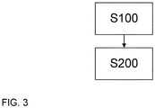
- Figure 3 schematically illustrates the steps performed in the method of improving Transmission Kikuchi, TKD, patterns according to the present invention.
- a TKD pattern of sample 12 is detected in the electron microscope 60 as described already above with respect to Figure 2 .
- the electron lens 61 of EM 60 focusses the electron beam 80 in z-direction on the sample 12 positioned in distance D below the electron lens 61 via the sample holder 10.
- the diffracted electrons 82 exiting the sample 12 via a rear side thereof facing the TKD detector 64 are detected via the phosphor screen 65 of the TKD detector 64.
- the detected TKD pattern 20b is distorted by the magnetic field of the electron lens 61 and hence comprises a plurality of warped Diffraction bands 21b as shown in Figure 1B .
- the detected Kikuchi pattern comprises a plurality of image points with the coordinates x D and y D .
- step S200 an improved TKD pattern is calculated based on the TKD pattern detected in step S100.
- These mapping of the disturbed TKD pattern on the improved (undisturbed) TKD patterns is performed using the generalized terms that are mapping each of the image points x 0 , y 0 of an undisturbed (improved) TKD pattern onto image points x D , y D of a corresponding detected (disturbed) TKD pattern.
- a magnetic field of the electron lens is approximated for a reference system with a coordinate system origin being located in the intersection point between the electron beam and the sample.
- the positive z-direction points downwards, i.e., in the propagation direction of the electron beam, such that the x- and y- directions are positioned in the horizontal plane of the reference system.
- the origin of the coordinate system is centred on the lower sample surface.
- the magnetic field is thus parallel to the z-direction and is considered to be at least partially constant.
- equation of motion is only presented herein as intermediate step to deriving the generalized terms actually used for improving the TKD patterns in the method of the present invention, particularly using a parameter set based on a calibration pattern. However, no equations of motion are used in the method of the invention.
- the trigonometric expression A is of the form x 0 sin ⁇ ⁇ + y 0 1 ⁇ cos ⁇ ⁇
- the trigonometric expression B is of the form x 0 cos ⁇ + y 0 sin ⁇
- the trigonometric expression C is of the form ⁇ x 0 1 ⁇ cos ⁇ ⁇ + + y 0 sin ⁇ ⁇
- the trigonometric expression D is of the form ⁇ x 0 sin ⁇ + y 0 cos ⁇ .
Landscapes
- Chemical & Material Sciences (AREA)
- Analytical Chemistry (AREA)
- Crystallography & Structural Chemistry (AREA)
- Physics & Mathematics (AREA)
- Health & Medical Sciences (AREA)
- Life Sciences & Earth Sciences (AREA)
- Biochemistry (AREA)
- General Health & Medical Sciences (AREA)
- General Physics & Mathematics (AREA)
- Immunology (AREA)
- Pathology (AREA)
- Analysing Materials By The Use Of Radiation (AREA)
Priority Applications (3)
| Application Number | Priority Date | Filing Date | Title |
|---|---|---|---|
| EP19216196.6A EP3835768B1 (en) | 2019-12-13 | 2019-12-13 | Method for improving kikuchi diffraction patterns |
| JP2020199270A JP7228558B2 (ja) | 2019-12-13 | 2020-12-01 | 透過菊池回折パターンの改良方法 |
| US17/114,202 US11270867B2 (en) | 2019-12-13 | 2020-12-07 | Method for improving transmission Kikuchi diffraction pattern |
Applications Claiming Priority (1)
| Application Number | Priority Date | Filing Date | Title |
|---|---|---|---|
| EP19216196.6A EP3835768B1 (en) | 2019-12-13 | 2019-12-13 | Method for improving kikuchi diffraction patterns |
Publications (2)
| Publication Number | Publication Date |
|---|---|
| EP3835768A1 EP3835768A1 (en) | 2021-06-16 |
| EP3835768B1 true EP3835768B1 (en) | 2021-10-27 |
Family
ID=68917374
Family Applications (1)
| Application Number | Title | Priority Date | Filing Date |
|---|---|---|---|
| EP19216196.6A Active EP3835768B1 (en) | 2019-12-13 | 2019-12-13 | Method for improving kikuchi diffraction patterns |
Country Status (3)
| Country | Link |
|---|---|
| US (1) | US11270867B2 (enExample) |
| EP (1) | EP3835768B1 (enExample) |
| JP (1) | JP7228558B2 (enExample) |
Families Citing this family (6)
| Publication number | Priority date | Publication date | Assignee | Title |
|---|---|---|---|---|
| EP3736561B1 (en) * | 2019-05-08 | 2021-05-05 | Bruker Nano GmbH | Method for improving an ebsd/tkd map |
| EP3770945B1 (en) * | 2019-07-26 | 2024-06-19 | Bruker Nano GmbH | Kikuchi diffraction detector |
| EP3835768B1 (en) * | 2019-12-13 | 2021-10-27 | Bruker Nano GmbH | Method for improving kikuchi diffraction patterns |
| CN113720865B (zh) * | 2021-08-06 | 2022-09-02 | 清华大学 | 自动矫正样品带轴偏离的电子层叠成像方法及装置 |
| GB202208289D0 (en) * | 2022-06-06 | 2022-07-20 | Oxford Instruments Nanotechnology Tools Ltd | Ebsd data enhancement using simulated pattern matching |
| US11996264B1 (en) * | 2023-09-06 | 2024-05-28 | Honeywell Federal Manufacturing & Technologies, Llc | Sample mount for electron backscatter diffraction |
Family Cites Families (11)
| Publication number | Priority date | Publication date | Assignee | Title |
|---|---|---|---|---|
| US6555817B1 (en) * | 2000-05-17 | 2003-04-29 | Thermo Noran Inc. | Method and apparatus for correcting magnetic field distortions in electron backscatter diffraction patterns obtained in an electron microscope |
| GB0506907D0 (en) * | 2005-04-05 | 2005-05-11 | Oxford Instr Analytical Ltd | Method for correcting distortions in electron backscatter diffraction patterns |
| GB201302694D0 (en) * | 2013-02-15 | 2013-04-03 | Oxford Instr Nanotechnology Tools Ltd | Method of electron beam diffraction analysis |
| GB201402318D0 (en) * | 2014-02-11 | 2014-03-26 | Oxford Instr Nanotechnology Tools Ltd | Method for materials analysis |
| DE102014208295A1 (de) * | 2014-05-02 | 2015-11-05 | Bruker Nano Gmbh | Verfahren und Anordnung zur Identifikation kristalliner Phasen sowie ein entsprechendes Computerprogramm und ein entsprechendes computerlesbares Speichermedium |
| DE102014226985B4 (de) * | 2014-12-23 | 2024-02-08 | Carl Zeiss Microscopy Gmbh | Verfahren zum Analysieren eines Objekts, Computerprogrammprodukt sowie Teilchenstrahlgerät zur Durchführung des Verfahrens |
| EP3121593B1 (en) * | 2015-07-23 | 2023-11-08 | Carl Zeiss Microscopy GmbH | Method of determining crystallographic properties of a sample and electron beam microscope for performing the method |
| FR3074949B1 (fr) * | 2017-12-11 | 2019-12-20 | Electricite De France | Procede, dispositif et programme de traitement d'images de diffraction d'un materiau cristallin |
| JP7187685B2 (ja) * | 2019-04-23 | 2022-12-12 | 株式会社日立ハイテク | 荷電粒子線装置及び荷電粒子線装置の制御方法 |
| EP3770945B1 (en) * | 2019-07-26 | 2024-06-19 | Bruker Nano GmbH | Kikuchi diffraction detector |
| EP3835768B1 (en) * | 2019-12-13 | 2021-10-27 | Bruker Nano GmbH | Method for improving kikuchi diffraction patterns |
-
2019
- 2019-12-13 EP EP19216196.6A patent/EP3835768B1/en active Active
-
2020
- 2020-12-01 JP JP2020199270A patent/JP7228558B2/ja active Active
- 2020-12-07 US US17/114,202 patent/US11270867B2/en active Active
Also Published As
| Publication number | Publication date |
|---|---|
| US20210183612A1 (en) | 2021-06-17 |
| US11270867B2 (en) | 2022-03-08 |
| JP7228558B2 (ja) | 2023-02-24 |
| JP2021097039A (ja) | 2021-06-24 |
| EP3835768A1 (en) | 2021-06-16 |
Similar Documents
| Publication | Publication Date | Title |
|---|---|---|
| EP3835768B1 (en) | Method for improving kikuchi diffraction patterns | |
| KR102277028B1 (ko) | 회절 패턴을 이용한 샘플 정렬 시스템 | |
| EP1365229B1 (en) | Electron nano diffraction method of measuring strain and stress by detecting one or a plurality of diffraction spots | |
| Liu | Advances and applications of atomic-resolution scanning transmission electron microscopy | |
| US9396907B2 (en) | Method of calibrating a scanning transmission charged-particle microscope | |
| Wannberg | Electron optics development for photo-electron spectrometers | |
| US10636622B2 (en) | Scanning transmission electron microscope | |
| JP5132895B2 (ja) | 後方散乱電子回折パターンの歪みを修正する方法 | |
| TWI768191B (zh) | 用於自動對準掃描透射電子顯微鏡以便旋進電子衍射資料映射的方法 | |
| US10627354B2 (en) | Substitution site measuring equipment and substitution site measuring method | |
| EP3392900B1 (en) | A method for automatically aligning a scanning transmission electron microscope for precession electron diffraction data mapping | |
| US20240192152A1 (en) | Information processing system and phase analysis system | |
| JP5397060B2 (ja) | 荷電粒子顕微鏡及び解析方法 | |
| JPH08153485A (ja) | 荷電粒子線の偏向角測定方法及び荷電粒子線装置 | |
| EP3142139B1 (en) | Charged particle beam system and measuring method | |
| JPWO2007125652A1 (ja) | 電子顕微鏡とその対物レンズ系収差特性の計測方法 | |
| JP2001093459A (ja) | 走査透過型電子顕微鏡 | |
| Goehner et al. | Appllied crystallography in the scanning electron microscope using a CCD detector | |
| JP2010016007A (ja) | 荷電粒子線調整方法及び荷電粒子線装置 | |
| JP2008282826A (ja) | 荷電粒子線調整方法、及び荷電粒子線装置 | |
| JP2010153315A (ja) | 電子線装置および電子線装置における浮遊磁場測定方法 | |
| WO2012136993A1 (en) | Methods, apparatuses and computer programs for crystallography | |
| Reimer | Electron diffraction modes and applications |
Legal Events
| Date | Code | Title | Description |
|---|---|---|---|
| STAA | Information on the status of an ep patent application or granted ep patent |
Free format text: STATUS: EXAMINATION IS IN PROGRESS |
|
| PUAI | Public reference made under article 153(3) epc to a published international application that has entered the european phase |
Free format text: ORIGINAL CODE: 0009012 |
|
| 17P | Request for examination filed |
Effective date: 20200611 |
|
| AK | Designated contracting states |
Kind code of ref document: A1 Designated state(s): AL AT BE BG CH CY CZ DE DK EE ES FI FR GB GR HR HU IE IS IT LI LT LU LV MC MK MT NL NO PL PT RO RS SE SI SK SM TR |
|
| GRAP | Despatch of communication of intention to grant a patent |
Free format text: ORIGINAL CODE: EPIDOSNIGR1 |
|
| STAA | Information on the status of an ep patent application or granted ep patent |
Free format text: STATUS: GRANT OF PATENT IS INTENDED |
|
| INTG | Intention to grant announced |
Effective date: 20210719 |
|
| GRAS | Grant fee paid |
Free format text: ORIGINAL CODE: EPIDOSNIGR3 |
|
| GRAA | (expected) grant |
Free format text: ORIGINAL CODE: 0009210 |
|
| STAA | Information on the status of an ep patent application or granted ep patent |
Free format text: STATUS: THE PATENT HAS BEEN GRANTED |
|
| AK | Designated contracting states |
Kind code of ref document: B1 Designated state(s): AL AT BE BG CH CY CZ DE DK EE ES FI FR GB GR HR HU IE IS IT LI LT LU LV MC MK MT NL NO PL PT RO RS SE SI SK SM TR |
|
| REG | Reference to a national code |
Ref country code: GB Ref legal event code: FG4D |
|
| REG | Reference to a national code |
Ref country code: CH Ref legal event code: EP |
|
| REG | Reference to a national code |
Ref country code: AT Ref legal event code: REF Ref document number: 1442227 Country of ref document: AT Kind code of ref document: T Effective date: 20211115 |
|
| REG | Reference to a national code |
Ref country code: DE Ref legal event code: R096 Ref document number: 602019008723 Country of ref document: DE |
|
| REG | Reference to a national code |
Ref country code: IE Ref legal event code: FG4D |
|
| REG | Reference to a national code |
Ref country code: NL Ref legal event code: FP |
|
| REG | Reference to a national code |
Ref country code: LT Ref legal event code: MG9D |
|
| REG | Reference to a national code |
Ref country code: AT Ref legal event code: MK05 Ref document number: 1442227 Country of ref document: AT Kind code of ref document: T Effective date: 20211027 |
|
| PG25 | Lapsed in a contracting state [announced via postgrant information from national office to epo] |
Ref country code: RS Free format text: LAPSE BECAUSE OF FAILURE TO SUBMIT A TRANSLATION OF THE DESCRIPTION OR TO PAY THE FEE WITHIN THE PRESCRIBED TIME-LIMIT Effective date: 20211027 Ref country code: LT Free format text: LAPSE BECAUSE OF FAILURE TO SUBMIT A TRANSLATION OF THE DESCRIPTION OR TO PAY THE FEE WITHIN THE PRESCRIBED TIME-LIMIT Effective date: 20211027 Ref country code: FI Free format text: LAPSE BECAUSE OF FAILURE TO SUBMIT A TRANSLATION OF THE DESCRIPTION OR TO PAY THE FEE WITHIN THE PRESCRIBED TIME-LIMIT Effective date: 20211027 Ref country code: BG Free format text: LAPSE BECAUSE OF FAILURE TO SUBMIT A TRANSLATION OF THE DESCRIPTION OR TO PAY THE FEE WITHIN THE PRESCRIBED TIME-LIMIT Effective date: 20220127 Ref country code: AT Free format text: LAPSE BECAUSE OF FAILURE TO SUBMIT A TRANSLATION OF THE DESCRIPTION OR TO PAY THE FEE WITHIN THE PRESCRIBED TIME-LIMIT Effective date: 20211027 |
|
| PG25 | Lapsed in a contracting state [announced via postgrant information from national office to epo] |
Ref country code: IS Free format text: LAPSE BECAUSE OF FAILURE TO SUBMIT A TRANSLATION OF THE DESCRIPTION OR TO PAY THE FEE WITHIN THE PRESCRIBED TIME-LIMIT Effective date: 20220227 Ref country code: SE Free format text: LAPSE BECAUSE OF FAILURE TO SUBMIT A TRANSLATION OF THE DESCRIPTION OR TO PAY THE FEE WITHIN THE PRESCRIBED TIME-LIMIT Effective date: 20211027 Ref country code: PT Free format text: LAPSE BECAUSE OF FAILURE TO SUBMIT A TRANSLATION OF THE DESCRIPTION OR TO PAY THE FEE WITHIN THE PRESCRIBED TIME-LIMIT Effective date: 20220228 Ref country code: PL Free format text: LAPSE BECAUSE OF FAILURE TO SUBMIT A TRANSLATION OF THE DESCRIPTION OR TO PAY THE FEE WITHIN THE PRESCRIBED TIME-LIMIT Effective date: 20211027 Ref country code: NO Free format text: LAPSE BECAUSE OF FAILURE TO SUBMIT A TRANSLATION OF THE DESCRIPTION OR TO PAY THE FEE WITHIN THE PRESCRIBED TIME-LIMIT Effective date: 20220127 Ref country code: LV Free format text: LAPSE BECAUSE OF FAILURE TO SUBMIT A TRANSLATION OF THE DESCRIPTION OR TO PAY THE FEE WITHIN THE PRESCRIBED TIME-LIMIT Effective date: 20211027 Ref country code: HR Free format text: LAPSE BECAUSE OF FAILURE TO SUBMIT A TRANSLATION OF THE DESCRIPTION OR TO PAY THE FEE WITHIN THE PRESCRIBED TIME-LIMIT Effective date: 20211027 Ref country code: GR Free format text: LAPSE BECAUSE OF FAILURE TO SUBMIT A TRANSLATION OF THE DESCRIPTION OR TO PAY THE FEE WITHIN THE PRESCRIBED TIME-LIMIT Effective date: 20220128 Ref country code: ES Free format text: LAPSE BECAUSE OF FAILURE TO SUBMIT A TRANSLATION OF THE DESCRIPTION OR TO PAY THE FEE WITHIN THE PRESCRIBED TIME-LIMIT Effective date: 20211027 |
|
| REG | Reference to a national code |
Ref country code: DE Ref legal event code: R097 Ref document number: 602019008723 Country of ref document: DE |
|
| PG25 | Lapsed in a contracting state [announced via postgrant information from national office to epo] |
Ref country code: SM Free format text: LAPSE BECAUSE OF FAILURE TO SUBMIT A TRANSLATION OF THE DESCRIPTION OR TO PAY THE FEE WITHIN THE PRESCRIBED TIME-LIMIT Effective date: 20211027 Ref country code: SK Free format text: LAPSE BECAUSE OF FAILURE TO SUBMIT A TRANSLATION OF THE DESCRIPTION OR TO PAY THE FEE WITHIN THE PRESCRIBED TIME-LIMIT Effective date: 20211027 Ref country code: RO Free format text: LAPSE BECAUSE OF FAILURE TO SUBMIT A TRANSLATION OF THE DESCRIPTION OR TO PAY THE FEE WITHIN THE PRESCRIBED TIME-LIMIT Effective date: 20211027 Ref country code: MC Free format text: LAPSE BECAUSE OF FAILURE TO SUBMIT A TRANSLATION OF THE DESCRIPTION OR TO PAY THE FEE WITHIN THE PRESCRIBED TIME-LIMIT Effective date: 20211027 Ref country code: EE Free format text: LAPSE BECAUSE OF FAILURE TO SUBMIT A TRANSLATION OF THE DESCRIPTION OR TO PAY THE FEE WITHIN THE PRESCRIBED TIME-LIMIT Effective date: 20211027 Ref country code: DK Free format text: LAPSE BECAUSE OF FAILURE TO SUBMIT A TRANSLATION OF THE DESCRIPTION OR TO PAY THE FEE WITHIN THE PRESCRIBED TIME-LIMIT Effective date: 20211027 |
|
| PLBE | No opposition filed within time limit |
Free format text: ORIGINAL CODE: 0009261 |
|
| STAA | Information on the status of an ep patent application or granted ep patent |
Free format text: STATUS: NO OPPOSITION FILED WITHIN TIME LIMIT |
|
| REG | Reference to a national code |
Ref country code: BE Ref legal event code: MM Effective date: 20211231 |
|
| 26N | No opposition filed |
Effective date: 20220728 |
|
| PG25 | Lapsed in a contracting state [announced via postgrant information from national office to epo] |
Ref country code: LU Free format text: LAPSE BECAUSE OF NON-PAYMENT OF DUE FEES Effective date: 20211213 Ref country code: IE Free format text: LAPSE BECAUSE OF NON-PAYMENT OF DUE FEES Effective date: 20211213 Ref country code: AL Free format text: LAPSE BECAUSE OF FAILURE TO SUBMIT A TRANSLATION OF THE DESCRIPTION OR TO PAY THE FEE WITHIN THE PRESCRIBED TIME-LIMIT Effective date: 20211027 |
|
| PG25 | Lapsed in a contracting state [announced via postgrant information from national office to epo] |
Ref country code: FR Free format text: LAPSE BECAUSE OF NON-PAYMENT OF DUE FEES Effective date: 20211227 Ref country code: BE Free format text: LAPSE BECAUSE OF NON-PAYMENT OF DUE FEES Effective date: 20211231 |
|
| PG25 | Lapsed in a contracting state [announced via postgrant information from national office to epo] |
Ref country code: IT Free format text: LAPSE BECAUSE OF FAILURE TO SUBMIT A TRANSLATION OF THE DESCRIPTION OR TO PAY THE FEE WITHIN THE PRESCRIBED TIME-LIMIT Effective date: 20211027 |
|
| P01 | Opt-out of the competence of the unified patent court (upc) registered |
Effective date: 20230505 |
|
| PG25 | Lapsed in a contracting state [announced via postgrant information from national office to epo] |
Ref country code: CY Free format text: LAPSE BECAUSE OF FAILURE TO SUBMIT A TRANSLATION OF THE DESCRIPTION OR TO PAY THE FEE WITHIN THE PRESCRIBED TIME-LIMIT Effective date: 20211027 |
|
| PG25 | Lapsed in a contracting state [announced via postgrant information from national office to epo] |
Ref country code: HU Free format text: LAPSE BECAUSE OF FAILURE TO SUBMIT A TRANSLATION OF THE DESCRIPTION OR TO PAY THE FEE WITHIN THE PRESCRIBED TIME-LIMIT; INVALID AB INITIO Effective date: 20191213 |
|
| REG | Reference to a national code |
Ref country code: CH Ref legal event code: PL |
|
| PG25 | Lapsed in a contracting state [announced via postgrant information from national office to epo] |
Ref country code: SI Free format text: LAPSE BECAUSE OF FAILURE TO SUBMIT A TRANSLATION OF THE DESCRIPTION OR TO PAY THE FEE WITHIN THE PRESCRIBED TIME-LIMIT Effective date: 20211027 |
|
| PG25 | Lapsed in a contracting state [announced via postgrant information from national office to epo] |
Ref country code: LI Free format text: LAPSE BECAUSE OF NON-PAYMENT OF DUE FEES Effective date: 20221231 Ref country code: CH Free format text: LAPSE BECAUSE OF NON-PAYMENT OF DUE FEES Effective date: 20221231 |
|
| PG25 | Lapsed in a contracting state [announced via postgrant information from national office to epo] |
Ref country code: MK Free format text: LAPSE BECAUSE OF FAILURE TO SUBMIT A TRANSLATION OF THE DESCRIPTION OR TO PAY THE FEE WITHIN THE PRESCRIBED TIME-LIMIT Effective date: 20211027 |
|
| PG25 | Lapsed in a contracting state [announced via postgrant information from national office to epo] |
Ref country code: TR Free format text: LAPSE BECAUSE OF FAILURE TO SUBMIT A TRANSLATION OF THE DESCRIPTION OR TO PAY THE FEE WITHIN THE PRESCRIBED TIME-LIMIT Effective date: 20211027 |
|
| PG25 | Lapsed in a contracting state [announced via postgrant information from national office to epo] |
Ref country code: MT Free format text: LAPSE BECAUSE OF FAILURE TO SUBMIT A TRANSLATION OF THE DESCRIPTION OR TO PAY THE FEE WITHIN THE PRESCRIBED TIME-LIMIT Effective date: 20211027 |
|
| PGFP | Annual fee paid to national office [announced via postgrant information from national office to epo] |
Ref country code: DE Payment date: 20241121 Year of fee payment: 6 |
|
| PGFP | Annual fee paid to national office [announced via postgrant information from national office to epo] |
Ref country code: NL Payment date: 20241217 Year of fee payment: 6 |
|
| PGFP | Annual fee paid to national office [announced via postgrant information from national office to epo] |
Ref country code: GB Payment date: 20241218 Year of fee payment: 6 |
|
| PGFP | Annual fee paid to national office [announced via postgrant information from national office to epo] |
Ref country code: CZ Payment date: 20241129 Year of fee payment: 6 |