EP3796458B1 - Batteriepack - Google Patents
Batteriepack Download PDFInfo
- Publication number
- EP3796458B1 EP3796458B1 EP19803122.1A EP19803122A EP3796458B1 EP 3796458 B1 EP3796458 B1 EP 3796458B1 EP 19803122 A EP19803122 A EP 19803122A EP 3796458 B1 EP3796458 B1 EP 3796458B1
- Authority
- EP
- European Patent Office
- Prior art keywords
- connection pad
- portions
- end portion
- soldering
- board connection
- Prior art date
- Legal status (The legal status is an assumption and is not a legal conclusion. Google has not performed a legal analysis and makes no representation as to the accuracy of the status listed.)
- Active
Links
Images


Classifications
-
- H—ELECTRICITY
- H01—ELECTRIC ELEMENTS
- H01M—PROCESSES OR MEANS, e.g. BATTERIES, FOR THE DIRECT CONVERSION OF CHEMICAL ENERGY INTO ELECTRICAL ENERGY
- H01M10/00—Secondary cells; Manufacture thereof
- H01M10/42—Methods or arrangements for servicing or maintenance of secondary cells or secondary half-cells
- H01M10/425—Structural combination with electronic components, e.g. electronic circuits integrated to the outside of the casing
-
- H—ELECTRICITY
- H01—ELECTRIC ELEMENTS
- H01M—PROCESSES OR MEANS, e.g. BATTERIES, FOR THE DIRECT CONVERSION OF CHEMICAL ENERGY INTO ELECTRICAL ENERGY
- H01M10/00—Secondary cells; Manufacture thereof
- H01M10/42—Methods or arrangements for servicing or maintenance of secondary cells or secondary half-cells
- H01M10/48—Accumulators combined with arrangements for measuring, testing or indicating the condition of cells, e.g. the level or density of the electrolyte
- H01M10/482—Accumulators combined with arrangements for measuring, testing or indicating the condition of cells, e.g. the level or density of the electrolyte for several batteries or cells simultaneously or sequentially
-
- H—ELECTRICITY
- H01—ELECTRIC ELEMENTS
- H01M—PROCESSES OR MEANS, e.g. BATTERIES, FOR THE DIRECT CONVERSION OF CHEMICAL ENERGY INTO ELECTRICAL ENERGY
- H01M50/00—Constructional details or processes of manufacture of the non-active parts of electrochemical cells other than fuel cells, e.g. hybrid cells
- H01M50/20—Mountings; Secondary casings or frames; Racks, modules or packs; Suspension devices; Shock absorbers; Transport or carrying devices; Holders
- H01M50/204—Racks, modules or packs for multiple batteries or multiple cells
- H01M50/207—Racks, modules or packs for multiple batteries or multiple cells characterised by their shape
- H01M50/209—Racks, modules or packs for multiple batteries or multiple cells characterised by their shape adapted for prismatic or rectangular cells
-
- H—ELECTRICITY
- H01—ELECTRIC ELEMENTS
- H01M—PROCESSES OR MEANS, e.g. BATTERIES, FOR THE DIRECT CONVERSION OF CHEMICAL ENERGY INTO ELECTRICAL ENERGY
- H01M50/00—Constructional details or processes of manufacture of the non-active parts of electrochemical cells other than fuel cells, e.g. hybrid cells
- H01M50/20—Mountings; Secondary casings or frames; Racks, modules or packs; Suspension devices; Shock absorbers; Transport or carrying devices; Holders
- H01M50/284—Mountings; Secondary casings or frames; Racks, modules or packs; Suspension devices; Shock absorbers; Transport or carrying devices; Holders with incorporated circuit boards, e.g. printed circuit boards [PCB]
- H01M50/287—Fixing of circuit boards to lids or covers
-
- H—ELECTRICITY
- H01—ELECTRIC ELEMENTS
- H01M—PROCESSES OR MEANS, e.g. BATTERIES, FOR THE DIRECT CONVERSION OF CHEMICAL ENERGY INTO ELECTRICAL ENERGY
- H01M50/00—Constructional details or processes of manufacture of the non-active parts of electrochemical cells other than fuel cells, e.g. hybrid cells
- H01M50/20—Mountings; Secondary casings or frames; Racks, modules or packs; Suspension devices; Shock absorbers; Transport or carrying devices; Holders
- H01M50/298—Mountings; Secondary casings or frames; Racks, modules or packs; Suspension devices; Shock absorbers; Transport or carrying devices; Holders characterised by the wiring of battery packs
-
- H—ELECTRICITY
- H01—ELECTRIC ELEMENTS
- H01M—PROCESSES OR MEANS, e.g. BATTERIES, FOR THE DIRECT CONVERSION OF CHEMICAL ENERGY INTO ELECTRICAL ENERGY
- H01M50/00—Constructional details or processes of manufacture of the non-active parts of electrochemical cells other than fuel cells, e.g. hybrid cells
- H01M50/30—Arrangements for facilitating escape of gases
-
- H—ELECTRICITY
- H01—ELECTRIC ELEMENTS
- H01M—PROCESSES OR MEANS, e.g. BATTERIES, FOR THE DIRECT CONVERSION OF CHEMICAL ENERGY INTO ELECTRICAL ENERGY
- H01M50/00—Constructional details or processes of manufacture of the non-active parts of electrochemical cells other than fuel cells, e.g. hybrid cells
- H01M50/50—Current conducting connections for cells or batteries
- H01M50/502—Interconnectors for connecting terminals of adjacent batteries; Interconnectors for connecting cells outside a battery casing
- H01M50/514—Methods for interconnecting adjacent batteries or cells
- H01M50/516—Methods for interconnecting adjacent batteries or cells by welding, soldering or brazing
-
- B—PERFORMING OPERATIONS; TRANSPORTING
- B23—MACHINE TOOLS; METAL-WORKING NOT OTHERWISE PROVIDED FOR
- B23K—SOLDERING OR UNSOLDERING; WELDING; CLADDING OR PLATING BY SOLDERING OR WELDING; CUTTING BY APPLYING HEAT LOCALLY, e.g. FLAME CUTTING; WORKING BY LASER BEAM
- B23K2101/00—Articles made by soldering, welding or cutting
- B23K2101/36—Electric or electronic devices
- B23K2101/38—Conductors
-
- H—ELECTRICITY
- H01—ELECTRIC ELEMENTS
- H01M—PROCESSES OR MEANS, e.g. BATTERIES, FOR THE DIRECT CONVERSION OF CHEMICAL ENERGY INTO ELECTRICAL ENERGY
- H01M50/00—Constructional details or processes of manufacture of the non-active parts of electrochemical cells other than fuel cells, e.g. hybrid cells
- H01M50/20—Mountings; Secondary casings or frames; Racks, modules or packs; Suspension devices; Shock absorbers; Transport or carrying devices; Holders
- H01M50/262—Mountings; Secondary casings or frames; Racks, modules or packs; Suspension devices; Shock absorbers; Transport or carrying devices; Holders with fastening means, e.g. locks
- H01M50/264—Mountings; Secondary casings or frames; Racks, modules or packs; Suspension devices; Shock absorbers; Transport or carrying devices; Holders with fastening means, e.g. locks for cells or batteries, e.g. straps, tie rods or peripheral frames
-
- Y—GENERAL TAGGING OF NEW TECHNOLOGICAL DEVELOPMENTS; GENERAL TAGGING OF CROSS-SECTIONAL TECHNOLOGIES SPANNING OVER SEVERAL SECTIONS OF THE IPC; TECHNICAL SUBJECTS COVERED BY FORMER USPC CROSS-REFERENCE ART COLLECTIONS [XRACs] AND DIGESTS
- Y02—TECHNOLOGIES OR APPLICATIONS FOR MITIGATION OR ADAPTATION AGAINST CLIMATE CHANGE
- Y02E—REDUCTION OF GREENHOUSE GAS [GHG] EMISSIONS, RELATED TO ENERGY GENERATION, TRANSMISSION OR DISTRIBUTION
- Y02E60/00—Enabling technologies; Technologies with a potential or indirect contribution to GHG emissions mitigation
- Y02E60/10—Energy storage using batteries
Definitions
- the present disclosure relates to a battery pack.
- secondary batteries refer to batteries that can be repeatedly charged and recharged unlike non-rechargeable primary batteries. Secondary batteries are used as energy sources of devices such as mobile devices, electric vehicles, hybrid vehicles, electric bicycles, or uninterruptible power supplies. Secondary batteries are individually used or secondary battery modules each including a plurality of secondary batteries connected as one unit are used according to the types of external devices using secondary batteries.
- devices such as electric vehicles or hybrid vehicles having long operation times and consuming large amounts of electricity may prefer battery modules each including a plurality of batteries to handle problems relating to power and capacity, and the output voltages or currents of battery modules may be increased by adjusting the number of batteries included in each battery module.
- US 2012/0276419 A1 , EP 2 544 263 A1 and EP 2 842 797 A1 each relate to a battery pack.
- An embodiment of the present disclosure includes a battery pack according to claim 1, having a structure improved for stably maintaining electrical connection between a connection line and a circuit board with high reliability for transmitting state information about battery cells.
- An embodiment of the present disclosure includes a battery pack configured to save manufacturing costs through simple manufacturing processes.
- a battery pack of the present disclosure includes:
- the board connection pad may include:
- the outer soldering portions and the inner soldering portion may be formed by the conductive pattern exposed from the insulating layer.
- the conductive pattern may be a one-piece conductive pattern connected to all the outer soldering portions and the inner soldering portion formed on the board connection pad.
- each of the outer soldering portions may be formed in a semicircular shape having a center outside the board connection pad.
- the inner region may be surrounded by the outer region and may be separated from the outside of the board connection pad.
- the gas discharge hole may be formed in an elongated shape in the inner region of the board connection pad in a connection direction of the link line.
- the gas discharge hole may be formed in an oval shape having a long axis in the connection direction of the link line.
- the outer region of the board connection pad may include:
- the outer soldering portions may be formed on the second end portion, the third end portion, and the fourth end portion.
- an insulation-covered portion in which a conductive pattern of the board connection pad is covered with an insulating layer may be formed.
- the outer soldering portions formed on the third and fourth end portions may be symmetric.
- a total number of the outer soldering portions formed on the third and fourth end portions may be less than a total number of the outer soldering portions formed on the second end portion.
- a total number of the outer soldering portions, which are formed on the third and fourth end portions, and the inner soldering portion may be equal to a total number of the outer soldering portions formed on the second end portion.
- the outer soldering portions which are formed on the third and fourth end portions may not overlap the inner soldering portion in the connection direction of the link line.
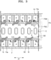
- the bus bar support portions FSB and the board support portions FSC may have different widths.
- the bus bar support portions FSB may be relatively narrow in order not to interfere electrical connection between the bus bars 15 and the battery cells B (specifically, the electrodes 10 of the battery cells B).
- the bus bar support portions FSB may support front and back end portions of the bus bars 15 which are located on both sides of bent portions 15a of the bus bars 15 and may insulate neighboring bus bars 15 from each other.
- the bus bar support portions FSB may support both end portions of the bus bars 15 and may electrically insulate neighboring bus bars 15 from each other such that both end portions of a bus bar 15 may not make contact with end portions of neighboring bus bars 15.
- the board support portions FSC have a relatively large width such that the circuit board C may be stably placed and supported on the board support portions FSC.
- the circuit board C may be placed on the board support portion FSC of each of the frames F, and the board support portions FSC of the frames F may be connected to each other in the forward/backward direction (corresponding to the direction Z1) to form a support surface widely extending in the forward/backward direction (corresponding to the direction Z1), thereby providing a support base for supporting the circuit board C.
- the circuit board C may collect state information, for example, voltage and temperature information, from the battery cells B and may transmit the state information to a separate battery management system (not shown) such that the separate battery management system (not shown) may control charge-discharge operations of the battery cells B, or the charge-discharge operations of the battery cells B may be controlled by a battery management system together with the circuit board C.
- state information for example, voltage and temperature information
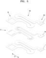
- the cell connection pad SI corresponds to a portion receiving state information from the side of the battery cell B (for example, from the bus bar 15 electrically connected to the battery cell B), and the board connection pad SO corresponds to a portion through which the state information about the battery cell B is output to the circuit board C.
- the link line SC connecting the cell connection pad SI and the board connection pad SO to each other may be formed in a curved shape having curved portions and overlapping portions.
- the cell connection pads SI of the connection lines S are connected to the battery cells B for acquiring state information such as the voltages or temperatures of the battery cells B, and for example, the cell connection pads SI are be connected to the bus bars 15 electrically connected to the battery cells B or the thermistors (not shown) thermally connected to the battery cells B.
- the cell connection pads SI may be welded to sides (for example, the bus bars) of the battery cells B.
- the cell connection pads SI may be ultrasonically welded to the bus bars 15 by placing the cell connection pads SI on the bus bars 15 and pressing an ultrasonic horn (not shown) against the cell connection pads SI to apply ultrasonic vibration to the cell connection pads SI.
- the cell connection pads SI and sides (for example, the bus bars 15) of the battery cells B may be coupled to each other using a conductive adhesive.
- Each of the link lines SC which connects the cell connection pad SI and the board connection pad SO to each other, may be formed in a curved shape having curved portions and overlapping portions.
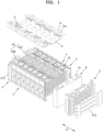
- the battery pack may include the frames F facing each other and coupled to each other with the battery cells B therebetween in the forward/backward direction (corresponding to the direction Z1) in which the battery cells B are arranged.
- the battery cells B may undergo swelling, that is, expansion, in the forward/backward direction (corresponding to the direction Z1), and in this case, the frames F which are forwardly and backwardly coupled to each other with the battery cells B therebetween may slide in the forward/backward direction (corresponding to the direction Z1) and accommodate deformation caused by the swelling of the battery cells B.
- the link lines SC connecting the cell connection pads SI and the board connection pads SO may deform to accommodate the deformation in the forward/backward direction (corresponding to the direction Z1).
- the link lines SC since the link lines SC have a curved shape with curved portions and overlapping portions, the link lines SC may be easily deformed according to the relative positions of the cell connection pads SI and the board connection pads SO which are moved away from each other because of the swelling, and thus stress may be less accumulated in the link lines SC.
- the board connection pads SO may be connected to pads (not shown) of the circuit board C, and electrical signals transmitted through the board connection pads SO may arrive at the conductive patterns (not shown) of the circuit board C via the pads (not shown) of the circuit board C. Specific structures of the board connection pads SO will be described later in more detail.
- reference numerals E and 210 refer to end blocks and end plates, respectively.
- the end blocks E and the end plates 210 may be placed on outer sides of the outermost battery cells B to provide fastening force for physically restraining the battery cells B of the battery pack.
- FIGS. 5 and 6 are an exploded perspective view and a plan view which illustrate a connection line S shown in FIG. 4 .
- connection line S may include: a conductive pattern M through which a signal providing state information about battery cells B such as voltage or temperature information is transmitted; and an insulating layer I in which the conductive pattern M is embedded.
- the insulating layer (I) may be formed on both surfaces of the conductive pattern M to insulate the conductive pattern M.
- the conductive pattern M may be formed in one piece across the entirety of the connection line S, which includes a cell connection pad SI and a board connection pad SO at both ends of the connection line S and a link line SC between the cell connection pad SI and the board connection pad SO, and the conductive pattern M may have a signal transmitting function to transmit state information about the battery cells B to the circuit board C.
- the insulating layer (I) may be formed on both sides of the conductive pattern M in one piece across the entirety of the connection line S, which includes the cell connection pad SI and the board connection pad SO at both ends of the connection line S and the link line SC between the cell connection pad SI and the board connection pad SO, but the insulating layer (I) may expose the conductive pattern M at a portion at which the cell connection pad SI is connected to a side of the battery cells B (for example, a bus bar 15 connected to the battery cells B) and a portion at which the board connection pad SO is connected to the circuit board C such that the connection line S is electrically connected to the side of the battery cells B (for example, the bus bar 15 connected to the battery cells B) and the circuit board C by performing a high-temperature thermal process such as welding or soldering between the side of the battery cells B (for example, the bus bar 15 connected to the battery cells B) and the portion of the conductive pattern M exposed from the insulating layer (I) and between the circuit board C and the portion of the conductive pattern
- An insulation-covered portion IC of the board connection pad SO at which the conductive pattern M is covered with the insulating layer (I) may not be directly coupled to the circuit board C, for example, in a state in which the insulation-covered portion IC is spaced apart from the circuit board C.
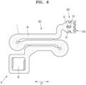
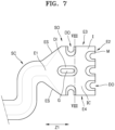
- FIG. 7 is an enlarged view illustrating a portion of the connection line S shown in FIG. 6 , to show a structure of the board connection pad SO.
- FIG. 8 is a cross-sectional view taken along line VIII-VIII of FIG. 7 .
- the board connection pad SO is formed in a shape widening as it goes in a connection direction (corresponding to the direction Z1) of the link line SC from a first end portion E1 connected to the link line SC such that the board connection pad SO may face the circuit board C over a relatively large area.
- the connection direction (corresponding to the direction Z1) of the link line SC may refer to a direction in which an end portion of the link line SC is connected to the first end portion E1 of the board connection pad SO but may not refer to the extension direction of the entirety of the link line SC having a plurality of curved portions. That is, the connection direction (corresponding to the direction Z1) of the link line SC may refer to the extension direction of the end portion of the link line SC connected to the board connection pad SO or the direction in which the end portion of the link line SC is connected to the board connection pad SO.
- the board connection pad SO may include the conductive pattern M and the insulating layer (I) in which the conductive pattern M is embedded, and in the board connection pad SO, the soldering portions DO and DI at which the conductive pattern M is exposed may be formed at positions different from the position of the insulation-covered portion IC at which the conductive pattern M is covered with the insulating layer (I).
- the soldering portions DO and DI may be formed by the conductive pattern M exposed from the insulating layer (I) and may be conductively connected to the circuit board C with solder SD therebetween.
- the insulation-covered portion IC may be a region in which the conductive pattern M is covered with the insulating layer (I) and is thus not directly connected to the circuit board C owing to the insulating layer (I) between the conductive pattern M and the circuit board C.
- the board connection pad SO and the circuit board C may be conductively connected to each other by reflow soldering.
- the reflow soldering may be performed by printing a pattern of solder paste or cream between the board connection pad SO and the circuit board C, performing a high-temperature thermal process to melt the solder paste or cream as molten or half-molten solder SD, and allowing the molten or half-molten solder SD to solidify between the board connection pad SO and the circuit board C for electrical connection between the board connection pad SO and the circuit board C.
- a pattern of solder paste or cream may be selectively printed on the soldering portions DO and DI of the board connection pad SO at which the conductive pattern M is exposed, and then the solder paste or crease melted as molten or half-molten solder SD through a high-temperature thermal process may form conductive connection between the circuit board C and the soldering portions DO and DI.
- soldering portions DO and DI at which the conductive pattern M is exposed from the insulating layer (I) may be securely coupled to the circuit board C, but the insulation-covered portion IC at which the conductive pattern M is covered with the insulating layer (I) may be separated or spaced apart from the circuit board C easily by external force instead of being coupled to the circuit board C.
- the soldering portions DO and DI are formed in outer and inner regions of the board connection pad SO.
- the outer region of the board connection pad SO may refer to a boundary region of the board connection pad SO which includes the first end portion E1 forming a boundary with the link line SC, a slope portion ES sloped from the first end portion E1 to increase the area of the board connection pad SO, a second end portion E2 on a side opposite the first end portion E1 in the connection direction of the link line SC, and third and fourth end portions E3 and E4 between the second end portion E2 and the slope portion ES.
- the outer soldering portion DO for coupling with the circuit board C may be formed on the second, third, and fourth end portions E2, E3, and E4.
- the outer soldering portion DO may be formed on the second, third, and fourth end portions E2, E3, and E4 by the conductive pattern M exposed from the insulating layer (I) such that solder SD may be provided between the circuit board C and the outer soldering portion DO.
- the outer soldering portion DO may be formed by a copper foil pattern having good wettability with solder SD.
- the outer soldering portion DO is formed along the outer region of the board connection pad SO, and more specifically, the outer soldering portion DO may include a plurality of outer soldering portions DO formed on the second, third, and fourth end portions E2, E3, and E4. Since the outer soldering portions DO are formed along the outer region of the board connection pad SO at a plurality of positions, the board connection pad SO and the circuit board C may be easily aligned with each other.
- the outer soldering portions DO may be formed in a round shape. More specifically, the outer soldering portions DO are formed in a shape concave toward the outside of the board connection pad SO. More specifically, the outer soldering portions DO may be formed by the conductive pattern M exposed from the insulating layer (I) such that solder SD melted through a high-temperature thermal process may be attached to the outer soldering portions DO, and end portions of the conductive pattern M exposed from the insulating layer (I) may be rounded with respect to the outside to from the outer soldering portions DO. For example, each of the outer soldering portions DO may be formed in a semicircular shape having a center outside the board connection pad SO.
- solder SD may be melted in the form of droplets having a spherical shape or a similar shape because of surface tension, and since the outer soldering portions DO making contact with the droplets of solder SD or the end portions of the conductive pattern M forming the outer soldering portions DO are rounded, the contact area between the outer soldering portions DO and the droplets of solder SD may increase.
- This shape design increasing the contact area between solder SD and the outer soldering portions DO may further facilitate self-alignment of the board connection pad SO and may increase the coupling strength between the board connection pad SO and the circuit board C.
- the outer soldering portions DO may be formed at a plurality of positions along the outer region of the board connection pad SO. More specifically, the outer soldering portions DO may be formed at three positions along the second end portion E2 of the board connection pad SO and at one position along each of the third and fourth end portions E3 and E4 of the board connection pad SO.
- the most outer soldering portions DO may be formed on the second end portion E2 of the board connection pad SO, and thus high coupling strength may be provided between the circuit board C and the second end portion E2 which is outmost in the connection direction (corresponding to the direction Z1) of the link line SC, such that the board connection pad SO may strongly resist deformation transmitted from the link line SC and may not be separated from the circuit board C due to deformation or force transmitted from the link line SC.
- the deformation or force transmitted from the link line SC may refer to deformation or force which is transmitted from the link line SC through the first end portion E1 of the board connection pad SO when the link line SC undergoes upward deformation in which a portion of the link line SC or the connection line S is lifted from a main plane.
- the most outer soldering portions DO are formed on the second end portion E2 of the board connection pad SO, whereas no outer soldering portion DO is formed on the first end portion E1 of the board connection pad SO and the slope portion ES close to the first end portion E1. That is, the insulation-covered portion IC at which the conductive pattern M is covered with the insulating layer (I) is formed on the first end portion E1 and the slope portion ES of the board connection pad SO, and the first end portion E1 and the slope portion ES at which the insulation-covered portion IC is formed is not directly coupled to the circuit board C. That is, unlike the outer soldering portions DO formed in the outer region other than the first end portion E1 and the slope portion ES, the first end portion E1 and the slope portion ES are not directly coupled to the circuit board C.
- This structure is provided by considering the possibility of breakage such as fatigue facture of the first end portion E1 caused by stress excessively accumulated in the first end portion E1 by deformation or repeated vibration of the link line SC when the first end portion E1, to which deformation or force is first transmitted from the link line SC, and the slope portion ES close to the first end portion E1 are firmly coupled to the circuit board C.
- No outer soldering portion DO is formed on the first end portion E1 of the board connection pad SO and the slope portion ES close to the first end portion E1, but the insulation-covered portion IC is formed on the first end portion E1 and the slope portion ES, such that the first end portion E1 and the slope portion ES of the board connection pad SO may be spaced apart from the circuit board C when the link line SC undergoes upward deformation. That is, deformation of the link line SC may be absorbed to some degree through lift-off deformation of the insulation-covered portion IC not coupled to the circuit board C, and stress concentrated on the first end portion E1 having the smallest width in the board connection pad SO may be released to some degree.
- outer soldering portions DO are symmetrically formed on the third and fourth end portions E3 and E4 which are opposite end portions of the board connection pad SO, thereby facilitating self-alignment of the board connection pad SO, guaranteeing balance of force through the symmetric outer soldering portions DO, and making it possible to guide the board connection pad SO to a balanced correct position.
- one outer soldering portion DO may be formed on each of the third and fourth end portions E3 and E4 of the board connection pad SO, and the number (for example, two) of outer soldering portions DO formed on the third and fourth end portions E3 and E4 may be less than the number (for example, three) of outer soldering portions DO formed on the second end portion E2 which is distant from the third and fourth end portions E3 and E4 in the connection direction (corresponding to the direction Z1) of the link line SC.
- the outer soldering portions DO are formed on the third and fourth end portions E3 and E4 at positions overlapping the inner soldering portion DI (refer to VIII-VIII line) in the connection direction (corresponding to the direction Z1) of the link line SC, and thus the outer soldering portions DO formed on the third and fourth end portions E3 and E4 may provide, in combination with the inner soldering portion DI, the same coupling strength as the coupling strength provided by the outer soldering portions DO formed on the second end portion E2.
- the gas discharge hole G is formed in the inner region of the board connection pad SO.
- a reflow soldering process may be performed by printing a pattern of solder paste or cream mixed with a solvent between the board connection pad SO and the circuit board C and performing a high-temperature thermal process to melt the solder paste or cream as molten solder SD and bond the board connection pad SO and the circuit board C to each other with the solder SD.
- the gas discharge hole G may provide a discharge path for volatile gas formed as the solvent mixed with the solder paste or cream evaporates in the high-temperature thermal process.
- the gas discharge hole G is formed in the inner region of the board connection pad SO.
- the inner region of the board connection pad SO may refer to a region surrounded by the outer region of the board connection pad SO. Since the outer region of the board connection pad SO is directly exposed to outer air, volatile gas may be directly discharged to the outer air even though no additional gas discharge hole G is formed in the outer region. In the inner region of the board connection pad SO, volatile gas may be discharged through the gas discharge hole G.
- gas which is not discharged from the inner region of the board connection pad SO and remains between the board connection pad SO and the circuit board C may hinder the coupling between the board connection pad SO and the circuit board C and may form defects such as pores while the molten solder SD solidifies, and thus the gas discharge hole G is formed in the inner region of the board connection pad SO to prevent soldering defects and increase the coupling strength between the board connection pad SO and the circuit board C.
- the gas discharge hole G may be formed in an elongated shape in one direction, for example, in the connection direction (corresponding to the direction Z1) of the link line SC.
- the gas discharge hole G since the gas discharge hole G has an elongated shape in the connection direction (corresponding to the direction Z1) of the link line SC, volatile gas generated at a plurality of positions in the inner region may be easily discharged to the outside.
- gas in the outer region of the board connection pad SO, gas may be directly discharged to outer air, and in the inner region of the board connection pad SO, gas may be discharged through the gas discharge hole G extending across the inner region of the board connection pad SO.
- the gas discharge hole G may be a long hole formed by partially removing both the conductive pattern M and the insulating layer (I) in the connection direction (corresponding to the direction Z1) of the link line SC.
- the inner soldering portion DI surrounding the gas discharge hole G may be formed together with the gas discharge hole G in the inner region of the board connection pad SO.
- the gas discharge hole G may be formed in a rounded oval shape extending in the connection direction (corresponding to the direction Z1) of the link line SC, and the inner soldering portion DI surrounding the gas discharge hole G may make contact with solder SD over a large area and may improve the coupling strength with the circuit board C.
- the inner soldering portion DI may be formed by the conductive pattern M exposed from the insulating layer (I) such that solder SD melted through a high-temperature thermal process may be attached to the inner soldering portion DI, and a portion of the conductive pattern M exposed from the insulating layer (I) may be formed in one direction in a round shape around the gas discharge hole G to from the inner soldering portion DI. That is, the gas discharge hole G may be formed by partially removing both the insulating layer (I) and the conductive pattern M, and the inner soldering portion DI may be formed around the gas discharge hole G by a portion of the conductive pattern M exposed from the insulating layer (I).
- the inner soldering portion DI is formed in the inner region of the board connection pad SO.
- the inner soldering portion DI may be formed in a closed loop shape surrounding the gas discharge hole G.
- the inner soldering portion DI may be formed by the conductive pattern M exposed from the insulating layer (I) such that solder SD may be provided between the inner soldering portion DI and the circuit board C.
- the inner soldering portion DI may be formed by a copper foil pattern having good wettability with solder SD.
- the inner soldering portion DI may extend in the connection direction (corresponding to the direction Z1) of the link line SC. More specifically, the inner soldering portion DI may extend in the connection direction (corresponding to the direction Z1) of the link line SC such that the inner soldering portion DI may effectively resist deformation tending to separate the board connection pad SO from the circuit board C in the connection direction (corresponding to the direction Z1) of the link line SC.
- the inner soldering portion DI may have a round shape extending in the connection direction (corresponding to the direction Z1) of the link line SC, and as a whole, the inner soldering portion DI may have an oval shape having a long axis in the connection direction (corresponding to the direction Z1) of the link line SC. Since the inner soldering portion DI has a round shape, the inner soldering portion DI may make contact with a large area of solder SD which is melted in a droplet shape due to surface tension.
- the most outer soldering portions DO may be formed on the second end portion E2 of the board connection pad SO, and one outer soldering portion DO may be formed on each other the third and fourth end portions E3 and E4.
- the inner soldering portion DI may be formed at a position overlapping the outer soldering portions DO of the third and fourth end portions E3 and E4 in the connection direction (corresponding to the direction Z1) of the link line SC (refer to line VIII-VIII), and the inner soldering portion DI and the outer soldering portions DO of the third and fourth end portions E3 and E4 may overlap each other along the same line.
- the total number of the inner soldering portion DI and the outer soldering portions DO of the third and fourth end portions E3 and E4 may be equal to the number (for example, three) of the outer soldering portions DO of the second end portion E2.
- the board connection pad SO may be formed by the conductive pattern M and the insulating layer (I) covering the conductive pattern M.
- the outer soldering portions DO formed in the outer region of the board connection pad SO, and the inner soldering portion DI formed in the inner region of the board connection pad SO may be formed by portions of the conductive pattern M exposed from the insulating layer (I), specifically as a copper foil pattern having high wettability with solder SD.
- the board connection pad SO which is a portion of the connection line S connecting the battery cells B and the circuit board C to each other, may be formed in one piece with the connection line S, and the conductive pattern M and the insulating layer (I) of the board connection pad SO may continuously extend from the connection line S (or the link line SC).
- connection line S may be formed as a flexible printed circuit board (FPCB) in the form of a film including the conductive pattern M and the insulating layer (I) in which the conductive pattern M is embedded.
- FPCB flexible printed circuit board
- the connection line S provided in the form of a film may undergo deformation in which a portion of the connection line S is lifted upward from a main plane, and this upward deformation of the connection line S may mainly occur in the link line SC which is freely connected between the cell connection pad SI and the board connection pad SO other than occurring in the cell connection pad SI and the board connection pad SO which are coupled to the battery cells B and the circuit board C.
- This upward deformation of the link line SC may be transmitted starting from the first end portion E1 of the board connection pad SO which adjoins the link line SC, to the board connection pad SO in the connection direction (corresponding to the direction Z1) of the link line SC, such that the upward deformation may function as a deformation or force separating the board connection pad SO from the circuit board C.
- no outer soldering portion DO is formed on the first end portion E1 of the board connection pad SO and the slope portion ES close to the first end portion E1, but the insulation-covered portion IC in which the conductive pattern M is covered with the insulating layer (I) is formed on the first end portion E1 and the slope portion ES, such that the first end portion E1 may be spaced apart from the circuit board C when the link line SC undergoes upward deformation. That is, deformation of the link line SC may be absorbed to some degree through lift-off deformation of the insulation-covered portion IC not coupled to the circuit board C, and stress concentrated on the first end portion E1 having the smallest width in the board connection pad SO may be released to some degree.
- the first end portion E1 or the slope portion ES of the board connection pad SO may excessively resist upward deformation of the link line SC, and stress may be concentrated on the first end portion E1 having the smallest width in the board connection pad SO. As a result, the first end portion E1 may break, for example, due to fatigue fracture caused by repeated upward deformation.
- the board connection pad SO may be securely coupled to the circuit board C without being separated from the circuit board C by upward deformation of the link line SC.
- the inner soldering portion DI since the inner soldering portion DI is formed in the inner region of the board connection pad SO which overlaps the third and fourth end portions E3 and E4, the inner soldering portion DI may be securely coupled to the circuit board C together with the outer soldering portions DO of the third and fourth end portions E3 and E4, and since the inner soldering portion DI extends in the connection direction (corresponding to the direction Z1) of the link line SC, the inner soldering portion DI may effectively resist upward deformation of the link line SC.
- the inner soldering portion DI and the outer soldering portions DO of the third and fourth end portions E3 and E4 are formed at positions overlapping each other in the connection direction (corresponding to the direction Z1) of the link line SC (refer to line VIII-VIII), and the outer soldering portions DO of the third and fourth end portions E3 and E4 and the inner soldering portion DI may provide high coupling strength with respect to the circuit board C together with the outer soldering portions DO formed on the second end portion E2.
- one outer soldering portion DO formed on each of the third and fourth end portions E3 and E4 and the inner soldering portion DI may provide the same coupling strength as the coupling strength provided by three outer soldering portions DO formed on the second end portion E2.
- the board connection pad SO may include: the conductive pattern M through battery cell state information is transmitted; and the insulating layer (I) in which the conductive pattern M is embedded and insulated.
- the conductive pattern M may be formed as an one-piece conductive pattern connected to all the outer soldering portions DO and the inner soldering portion DI of the board connection pad SO.
- a reflow soldering process may be performed by printing a pattern of solder paste or cream between the circuit board C and the board connection pad SO, melting the solder paste or cream as molten solder SD through a high-temperature thermal process, and coupling the circuit board C and the board connection pad SO to each other by solidifying the molten solder SD, and the outer soldering portions DO and the inner soldering portion DI may be formed in a round shape to increase a contact area with solder SD melted in the form of droplets due to surface tension.
- the outer soldering portions DO and the inner soldering portion DI may be formed by the conductive pattern M exposed from the insulating layer (I), and the expression "the outer soldering portions DO and the inner soldering portion DI are formed in a round shape" may mean that end portions of the conductive pattern M to be in contact with solder SD melted in the form of droplets are formed in a round shape.
- the outer soldering portions DO and the inner soldering portion DI may be formed by the conductive pattern M exposed form the insulating layer (I), and end portions of the conductive pattern M may be formed in a round shape.
- portions of the insulating layer (I) adjoining the outer soldering portions DO and the inner soldering portion DI may define the outer soldering portions DO and the inner soldering portion DI and may define contact regions with droplets of solder SD, and may be formed in a round shape by considering contact with droplets of solder SD.
- the outer soldering portions DO and the inner soldering portion DI may be formed by end portions of the conductive pattern M exposed from the round portions of the insulating layer (I), and in this case, the end portions of the conductive pattern M may be formed in a round shape.
- end portions of the insulating layer (I) adjoining the outer soldering portions DO and the inner soldering portion DI, and the end portions of the conductive pattern M forming the outer soldering portions DO and the inner soldering portion DI may have a round shape.
- a plurality of circuit elements may be mounted on the circuit board C to collect state information from battery cells and control the charge-discharge operations of the battery cells based on the collected state information, and all the circuit elements (not shown) may be conductively connected to the circuit board C in the reflow soldering process of the board connection pad SO. That is, in an embodiment of the present disclosure, coupling between the circuit board C and circuit elements (not shown), and coupling between the circuit board C and the board connection pad SO may be simultaneously performed through a single reflow soldering process.
- coupling between the board connection pad SO and the circuit board C may be performed through a process such as a hot-bar process requiring separate manufacturing equipment which is separate from a process (for example, a reflow soldering process) for coupling circuit elements to the circuit board C. That is, according to embodiments of the present disclosure, the number and complexity of manufacturing processes may be reduced by performing two different coupling tasks through a single process (for example, a reflow soldering process), and thus manufacturing costs may be efficiently used.
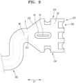
- FIG. 9 is a view illustrating a board connection pad SO applicable to another embodiment of the present disclosure.
- the board connection pad SO may include: a conductive pattern M through which state information about battery cells B is transmitted; and an insulating layer I in which the conductive pattern M is embedded.
- the board connection pad SO may include outer soldering portions DO and an inner soldering portion DI which are formed by portions of the conductive pattern M exposed from the insulating layer (I) for being coupled to the circuit board C with solder SD therebetween.
- the outer soldering portions DO and the inner soldering portion DI may be formed in a round shape for smooth contact with droplets of molten solder SD.
- portions of the insulating layer (I) adjoining the outer soldering portions DO and the inner soldering portion DI may define the outer soldering portions DO and the inner soldering portion DI and may define contact regions with droplets of solder SD.
- sufficient areas of the conductive pattern M may be exposed from the insulating layer (I) to form sufficient contact areas between solder SD and the outer soldering portions DO and the inner soldering portion DI, and to this end, the insulating layer (I) may be sufficiently recessed from end portions of the conductive pattern M.
- sufficient areas of the conductive pattern M may be exposed from the insulating layer (I), and end portions of the insulating layer (I) may be formed in an angled shape instead of a round shape as long as exposed portions of the conductive pattern M make contact with solder SD over sufficiently large areas.
- FIG. 10 is a view illustrating a board connection pad SO applicable to another embodiment of the present disclosure.
- the board connection pad SO may include an outer region as a boundary between the board connection pad SO and the outside, and an inner region surrounded by the outer region.
- the board connection pad SO may be coupled to the circuit board C through outer soldering portions DO1 to DO6 formed in the outer region and inner soldering portions DI1 and DI2 formed in the inner region.
- the outer region of the board connection pad SO may include: a first end portion E1 forming a boundary with the link line SC; a slope portion ES sloped from the first end portion E1 to increase the area of the board connection pad SO; a second end portion E2 on a side opposite the first end portion E1 in the connection direction (corresponding to the direction Z1) of the link line SC; and third and fourth end portions E3 and E4 between the second end portion E2 and the slope portion ES.
- first to fourth outer soldering portions DO1, DO2, DOS, and DO4 may be formed on the second end portion E2, and fifth and sixth outer soldering portions DO5 and DO6 may be respectively formed on the third and fourth end portions E3 and E4.
- first and second gas discharge holes G1 and G2 may be formed in the inner region of the board connection pad SO, and first and second inner soldering portions DI1 and DI2 may be formed respectively around the first and second gas discharge holes G1 and G2.
- Each of the first to sixth outer soldering portions DO1 to DO6 are concave toward the outside of the board connection pad SO and may have a semicircular shape having a center outside the board connection pad SO.
- the first and second gas discharge holes G1 and G2, and the first and second inner soldering portions DI1 and DI2 respectively surrounding the first and second gas discharge holes G1 and G2 may be rounded in an oval shape extending in the connection direction (corresponding to the direction Z1) of the link line SC.
- the board connection pad SO may include: conductive patterns M1 and M2 through which state information about battery cells B is transmitted; isolated patterns Y1 and Y2 through which state information about battery cells B is not transmitted; and an insulating layer (I) in which all the conductive patterns M1 and M2 and the isolated patterns Y1 and Y2 are embedded.
- the isolated patterns Y1 and Y2 may not transmit state information of battery cells B and may be isolated from the conductive patterns M1 and M2 without an electrical signal transmission function, and as described later, the isolated patterns Y1 and Y2 may include the third to sixth outer soldering portions DO3 to DO6 as structure for providing coupling strength with reference to the circuit board C.
- the conductive patterns M1 and M2 may have a transmission function for transmitting an electrical signal containing state information about battery cells B, and the conductive patterns M1 and M2 may also have a structural function for providing coupling strength with respect to the circuit board C by including the first and second outer soldering portions DO1 and DO2 and the first and second inner soldering portions DI1 and DI2.
- the conductive patterns M1 and M2 may include: a first conductive pattern M1 which connects the first outer soldering portion DO1 formed on the second end portion E2 to the first inner soldering portion DI1 surrounding the first gas discharge hole G1 formed in the inner region; and a second conductive pattern M2 which connects the second outer soldering portion DO2 formed on the second end portion E2 to the second inner soldering portion DI2 surrounding the second gas discharge hole G2 formed in the inner region.
- the isolated patterns Y1 and Y2 may include: a first isolated pattern Y1 which connects the third outer soldering portion DO3 formed on the second end portion E2 to the fifth outer soldering portion DO5 formed on the third end portion E3; and a second isolated pattern Y2 which connects the fourth outer soldering portion DO4 formed on the second end portion E2 to the sixth outer soldering portion DO6 formed on the fourth end portion E4.
- the first and second conductive patterns M1 and M2 may transmit state information about the same battery cell B and may be electrically connected to each other.
- the first and second conductive patterns M1 and M2 may be connected to each other in the board connection pad SO, or even when the first and second conductive patterns M1 and M2 are separated from each other in the board connection pad SO, the first and second conductive patterns M1 and M2 may be connected to each other in the link line SC.
- the first and second isolated patterns Y1 and Y2 are formed on the board connection pad SO in an isolated state and may not extend to the link line SC.
- the isolated patterns Y1 and Y2 which do not have a signal transmission function may be formed in addition to the conductive patterns M1 and M2 to increase the coupling strength between the board connection pad SO and the circuit board C, such that the coupling strength between the board connection pad SO and the circuit board C may be increased by the isolation patterns Y1 and Y2 without being limited to the minimum width of the first end portion E1.
- the isolated patterns Y1 and Y2 are formed only on the board connection pad SO and do not extend to the connection line SC, and even when the areas of the isolated patterns Y1 and Y2 are increased, the width of the first end portion E1 connected to the link line SC may not be affected by the isolated patterns Y1 and Y2.
- no soldering portion is formed on the first end portion E1 adjoining the link line SC and the slope portion ES adjoining the first end portion E1
- an insulation-covered portion IC in which the conductive patterns M1 and M2 are covered with the insulating layer (I) is formed at the first end portion E1 and the slope portion ES such that when upward deformation of the link line SC is transmitted to the first end portion E1, the first end portion E1 and the slope portion ES adjacent to the first end portion E1 may be deformed off the circuit board C according to the upward deformation of the link line SC to absorb the upward deformation of the link line SC to some degree and lower stress concentrated on the first end portion E1 forming the minimum width of the board connection pad SO.
- the fifth and sixth outer soldering portions DO5 and DO6 may be respectively formed on the third and fourth end portions E3 and E4 at positions overlapping the first and second inner soldering portions DI1 and DI2 in the connection direction (corresponding to the direction Z1) of the link line SC, and thus the total number (for example, four) of the fifth and sixth outer soldering portions DO5 and DO6 and the first and second inner soldering portions DI1 and DI2 may be equal to the total number (for example, four) of the first to fourth outer soldering portions DO1 to DO4 formed on the second end portion E2 such that the fifth and sixth outer soldering portions DO5 and DO6 and the first and second inner soldering portions DI1 and DI2 may provide the same coupling strength as the first to fourth outer soldering portions DO1 to DO4 formed on the second end portion E2.
- FIG. 11 is a view illustrating a board connection pad SO applicable to another embodiment of the present disclosure.
- the board connection pad SO may include an outer region as a boundary between the board connection pad SO and the outside, and an inner region surrounded by the outer region.
- the board connection pad SO may be coupled to the circuit board C through outer soldering portions DO1, DO2, DO3, and DO4 formed in the outer region and inner soldering portion DI1 and DI2 formed in the inner region.
- the outer region of the board connection pad SO may include: a first end portion E1 forming a boundary with the link line SC; a slope portion ES sloped from the first end portion E1 to increase the area of the board connection pad SO; a second end portion E2 on a side opposite the first end portion E1 in the connection direction (corresponding to the direction Z1) of the link line SC; and third and fourth end portions E3 and E4 between the second end portion E2 and the slope portion ES.
- first and second soldering portions DO1 and DO2 may be formed on the second end portion E2, and third and fourth outer soldering portions DO3 and DO4 may be respectively formed on the third and fourth end portions E3 and E4.
- first and second gas discharge holes G1 and G2 may be formed in the inner region of the board connection pad SO, and first and second inner soldering portions DI1 and DI2 may be formed respectively around the first and second gas discharge holes G1 and G2.
- Each of the first to fourth outer soldering portions DO1 to DO4 are concave toward the outside of the board connection pad SO and may have a semicircular shape having a center outside the board connection pad SO.
- the first and second gas discharge holes G1 and G2, and the first and second inner soldering portions DI1 and DI2 respectively surrounding the first and second gas discharge holes G1 and G2 may be rounded in an oval shape extending in the connection direction (corresponding to the direction Z1) of the link line SC.
- the board connection pad SO may include: conductive patterns M1 and M2 through which state information about battery cells B is transmitted; and an insulating layer (I) in which the conductive patterns M1 and M2 are embedded, wherein the conductive patterns M1 and M2 may include first and second conductive patterns M1 and M2 separated from each other.
- the first conductive pattern M1 may connect together the first outer soldering portion DO1 formed on the second end portion E2, the third outer soldering portion DO3 formed on the third end portion E3, and the first inner soldering portion DI1 surrounding the first gas discharge hole G1 formed in the inner region.
- the second conductive pattern M2 may connect together the second outer soldering portion DO2 formed on the second end portion E2, the fourth outer soldering portion DO4 formed on the fourth end portion E4, and the second inner soldering portion DI2 surrounding the second gas discharge hole G formed in the inner region.
- the first and second conductive patterns M1 and M2 may transmit state information about the same battery cell B and may be electrically connected to each other.
- the first and second conductive patterns M1 and M2 may be connected to each other in the board connection pad SO, or even when the first and second conductive patterns M1 and M2 are separated from each other in the board connection pad SO, the first and second conductive patterns M1 and M2 may be connected to each other in the link line SC.
- the conductive patterns M1 and M2 are not formed over the entire area of the board connection pad SO but are formed to be separate from each other based on a center line of the board connection pad SO, thereby reducing the areas of the conductive patterns M1 and M2 and material costs.
- the first and second conductive patterns M1 and M2 may be symmetric with respect to the center line of the board connection pad SO such that the board connection pad SO may be guided to a balanced correct position for facilitating self-alignment.
- no soldering portion is formed on the first end portion E1 connected to the link line SC and the slope portion ES adjoining the first end portion E1, and an insulation-covered portion IC in which the conductive patterns M1 and M2 are covered with the insulating layer (I) is formed at the first end portion E1 and the slope portion ES such that when upward deformation of the link line SC is transmitted to the first end portion E1, the first end portion E1 and the slope portion ES adjacent to the first end portion E1 may be deformed off the circuit board C according to the upward deformation of the link line SC to absorb the upward deformation of the link line SC to some degree and lower stress concentrated on the first end portion E1 forming the minimum width of the board connection pad SO.
- the third and fourth outer soldering portions DO3 and DO4 may be respectively formed on the third and fourth end portions E3 and E4 at overlapping positions in the connection direction (corresponding to the direction Z1) of the link line SC, and the first and second inner soldering portions DI1 and DI2 surrounding the first and second gas discharge holes G1 and G2 may also be formed at overlapping positions in the connection direction (corresponding to the direction Z1) of the link line SC.
- the total number (for example, two) of the third and fourth outer soldering portions DO3 and DO4 respectively formed on the third and fourth end portions E3 and E4 is equal to the total number (for example, two) of the first and second inner soldering portions DI1 and DI2 and the total number (for example, two) of the first and second outer soldering portions DO1 and DO2 formed on the second end portion E2.
- the third and fourth outer soldering portions DO3 and DO4 which overlap each other at positions apart from the first end portion E1 in the connection direction (corresponding to the direction Z1) of the link line SC, may provide coupling strength which is equivalent to coupling strength provided by the first and second inner soldering portions DI1 and DI2 overlapping each other and is equivalent to coupling strength provided by the first and second outer soldering portions DO1 and DO2 formed on the second end portion E2 which is farthest from the first end portion E1.
- the third and fourth outer soldering portions DO3 and DO4 formed on the third and fourth end portions E3 and E4 may not overlap the first and second inner soldering portions DI1 and DI2 in the connection direction (corresponding to the direction Z1) of the link line SC.
- the total number (for example, two) of the third and fourth outer soldering portions DO3 and DO4 formed on the third and fourth end portions E3 and E4 the total number (for example, two) of the first and second inner soldering portions DI1 and DI2
- the total number (for example, two) of the first and second outer soldering portions DO1 and DO2 formed on the second end portion E2 may be equal to each other.
- the present disclosure may be applied to battery packs which are rechargeable energy sources.
Landscapes
- Chemical & Material Sciences (AREA)
- Chemical Kinetics & Catalysis (AREA)
- Electrochemistry (AREA)
- General Chemical & Material Sciences (AREA)
- Engineering & Computer Science (AREA)
- Manufacturing & Machinery (AREA)
- Microelectronics & Electronic Packaging (AREA)
- Battery Mounting, Suspending (AREA)
- Connection Of Batteries Or Terminals (AREA)
Claims (15)
- Batteriepack, der Folgendes umfasst:eine Vielzahl von Batteriezellen (B), die in einer Vorwärts-/Rückwärtsrichtung entsprechend einer ersten Richtung (Z1) angeordnet sind;eine Leiterplatte (C), die zum Sammeln von Zustandsinformationen über die Batteriezellen (B) konfiguriert ist; undeine flexible Verbindungsleitung (S), die zum Übertragen der Zustandsinformationen über die Batteriezellen (B) an die Leiterplatte (C) konfiguriert ist und eine Verknüpfungsleitung (SC), ein Plattenverbindungspad (SO) und ein Zellenverbindungspad (SI) umfasst, wobei sich die Verknüpfungsleitung (SC) von einer Seite der Batteriezellen (B) zur Leiterplatte (C) hin erstreckt, sich das Plattenverbindungspad (SO) von einem ersten Endabschnitt (E1), mit dem die Verknüpfungsleitung (SC) verbunden ist, erstreckt und mit der Leiterplatte (C) gekoppelt ist, während es der Leiterplatte (C) zugewandt ist, und das Zellenverbindungspad (SI) mit einer Sammelschiene (15) verbunden ist, die die Zellen elektrisch verbindet,wobei das Plattenverbindungspad (SO) Folgendes umfasst:äußere Lötabschnitte (DO), die in einer äußeren Region des Plattenverbindungspads (SO) ausgebildet und zur Außenseite des Plattenverbindungspads (SO) hin konkav sind;ein Gasablassloch (G), das in Form einer geschlossenen Schleife in einer inneren Region des Plattenverbindungspads (SO) ausgebildet ist; undeinen inneren Lötabschnitt (DI), der entlang des Gasablasslochs (G) ausgebildet ist.
- Batteriepack nach Anspruch 1, wobei das Plattenverbindungspad (SO) Folgendes umfasst:ein leitfähiges Muster (M), durch das die Zustandsinformationen über die Batteriezellen (B) übertragen werden; undeine Isolierschicht (I), in die das leitende Muster (M) zum Isolieren eingebettet ist.
- Batteriepack nach Anspruch 2, wobei die äußeren Lötabschnitte (DO) und der innere Lötabschnitt (DI) durch das leitfähige Muster (M) gebildet werden, das von der Isolierschicht (I) freigelegt ist.
- Batteriepack nach Anspruch 2, wobei das leitfähige Muster (M) ein einteiliges leitfähiges Muster ist, das mit allen äußeren Lötabschnitten (DO) und dem inneren Lötabschnitt (DI) verbunden ist, die auf dem Plattenverbindungspad (SO) ausgebildet sind.
- Batteriepack nach Anspruch 1, wobei:(i) jeder der äußeren Lötabschnitte (DO) halbkreisförmig mit einer Mitte außerhalb des Plattenverbindungspads (SO) ausgebildet ist; und/oder(ii) die innere Region von der äußeren Region umgeben ist und von der Außenseite des Plattenverbindungspads (SO) getrennt ist.
- Batteriepack nach Anspruch 1, wobei das Gasablassloch (G) in einer länglichen Form in der inneren Region des Plattenverbindungspads (SO) in einer Verbindungsrichtung der Verknüpfungsleitung (SC) ausgebildet ist, die der ersten Richtung (Z1) entspricht, wobei das Gasablassloch (G) optional in einer ovalen Form mit einer langen Achse in der Verbindungsrichtung der Verknüpfungsleitung (SC) ausgebildet ist, die der ersten Richtung (Z1) entspricht.
- Batteriepack nach Anspruch 1, wobei die äußere Region des Plattenverbindungspads (SO) Folgendes umfasst:den ersten Endabschnitt (E1);einen Neigungsabschnitt (ES), der vom ersten Endabschnitt (E1) geneigt ist, um eine Fläche des Plattenverbindungspads (SO) zu vergrößern;einen zweiten Endabschnitt (E2) auf einer Seite gegenüber dem ersten Endabschnitt (E1) in einer Verbindungsrichtung der Verknüpfungsleitung (SC), die der ersten Richtung (Z1) entspricht; undeinen dritten Endabschnitt (E3) und einen vierten Endabschnitt (E4), die den zweiten Endabschnitt (E2) und den Neigungsabschnitt (ES) miteinander verbinden.
- Batteriepack nach Anspruch 7, wobei die äußeren Lötabschnitte (DO) auf dem zweiten Endabschnitt (E2), dem dritten Endabschnitt (E3) und dem vierten Endabschnitt (E4) ausgebildet sind.
- Batteriepack nach Anspruch 7, wobei im ersten Endabschnitt (E1) und im Neigungsabschnitt (ES) ein mit Isolationsstoff bedeckter Abschnitt (IC) ausgebildet ist, in dem ein leitfähiges Muster (M) des Plattenverbindungspads (SO) mit einer Isolierschicht (I) bedeckt ist.
- Batteriepack nach Anspruch 7, wobei die äußeren Lötabschnitte (DO) eine Vielzahl von auf dem zweiten Endabschnitt (E2) ausgebildeten äußeren Lötabschnitten (DO) umfassen.
- Batteriepack nach Anspruch 7, wobei:(i) die auf dem dritten und dem vierten Endabschnitt (E3, E4) ausgebildeten äußeren Lötabschnitte (DO) symmetrisch sind; und/oder(ii) eine Gesamtzahl der auf dem dritten und dem vierten Endabschnitt (E3, E4) ausgebildeten äußeren Lötabschnitte (DO) geringer ist als eine Gesamtzahl der auf dem zweiten Endabschnitt (E2) ausgebildeten äußeren Lötabschnitte (DO).
- Batteriepack nach Anspruch 7, wobei die auf dem dritten und dem vierten Endabschnitt (E3, E4) ausgebildeten äußeren Lötabschnitte (DO) den inneren Lötabschnitt (DI) in der Verbindungsrichtung der Verknüpfungsleitung (SC) überlappen, die der ersten Richtung (Z1) entspricht, wobei optional eine Gesamtzahl der äußeren Lötabschnitte (DO), die am dritten und am vierten Endabschnitt (E3, E4) ausgebildet sind, und dem inneren Lötabschnitt (DI) gleich einer Gesamtzahl der am zweiten Endabschnitt (E2) ausgebildeten äußeren Lötabschnitte (DO) ist.
- Batteriepack nach Anspruch 7, wobei die äußeren Lötabschnitte (DO), die am dritten und am vierten Endabschnitt (E3, E4) ausgebildet sind, den inneren Lötabschnitt (DI) in der Verbindungsrichtung der Verknüpfungsleitung (SC), die der ersten Richtung (Z1) entspricht, nicht überlappen, wobei optional eine Gesamtzahl der am dritten und am vierten Endabschnitt (E3, E4) ausgebildeten äußeren Lötabschnitte (DO) und eine Gesamtzahl der inneren Lötabschnitte (DI) jeweils gleich einer Gesamtzahl der am zweiten Endabschnitt (E2) ausgebildeten äußeren Lötabschnitte (DO) sind.
- Batteriepack nach Anspruch 7, wobeidas Plattenverbindungspad (SO) ein leitfähiges Muster (M), durch das die Zustandsinformationen über die Batteriezellen (B) übertragen werden, und ein isoliertes Muster (Y1, Y2), durch das die Zustandsinformationen über die Batteriezellen (B) nicht übertragen werden, umfasstwobei das leitfähige Muster (M) Folgendes umfasst:ein erstes leitfähiges Muster (M1), das einen auf dem zweiten Endabschnitt (E2) ausgebildeten ersten äußeren Lötabschnitt (DO1) mit einem ersten inneren Lötabschnitt (DI1) verbindet, der ein erstes Gasablassloch (G1) in der inneren Region umgibt; undein zweites leitfähiges Muster (M2), das einen auf dem zweiten Endabschnitt (E2) ausgebildeten zweiten äußeren Lötabschnitt (DO2) mit einem zweiten inneren Lötabschnitt (DI2) verbindet, der ein zweites Gasablassloch (G2) in der inneren Region umgibt,wobei das isolierte Muster (Y1, Y2) Folgendes umfasst:ein erstes isoliertes Muster (Y1), das einen auf dem zweiten Endabschnitt (E2) ausgebildeten dritten äußeren Lötabschnitt (DO3) mit einem auf dem dritten Endabschnitt (E3) ausgebildeten fünften äußeren Lötabschnitt (DO5) verbindet; undein zweites isoliertes Muster (Y2), das einen auf dem zweiten Endabschnitt (E2) ausgebildeten vierten äußeren Lötabschnitt (DO4) mit einem auf dem vierten Endabschnitt (E4) ausgebildeten sechsten äußeren Lötabschnitt (DO6) verbindet.
- Batteriepack nach Anspruch 7, wobeidas Plattenverbindungspad (SO) ein leitfähiges Muster (M) umfasst, durch das die Zustandsinformationen über die Batteriezellen (B) übertragen werden, und das leitfähige Muster (M) ein erstes und ein zweites leitfähiges Muster (M1, M2) umfasst, die voneinander getrennt sind,wobei das erste leitfähige Muster (M1) einen auf dem zweiten Endabschnitt (E2) ausgebildeten ersten äußeren Lötabschnitt (DO1), einen auf dem dritten Endabschnitt (E3) ausgebildeten dritten äußeren Lötabschnitt (DO3) und einen ein erstes Gasablassloch (G1) in der inneren Region umgebenden ersten inneren Lötabschnitt (DI1) miteinander verbindet, unddas zweite leitfähige Muster (M2) einen auf dem zweiten Endabschnitt (E2) ausgebildeten zweiten äußeren Lötabschnitt (DO2), einen auf dem vierten Endabschnitt (E4) ausgebildeten vierten äußeren Lötabschnitt (DO4) und einen ein zweites Gasablassloch (G2) in der inneren Region umgebenden zweiten inneren Lötabschnitt (DI2) miteinander verbindet.
Applications Claiming Priority (2)
| Application Number | Priority Date | Filing Date | Title |
|---|---|---|---|
| KR1020180055655A KR102562684B1 (ko) | 2018-05-15 | 2018-05-15 | 배터리 팩 |
| PCT/KR2019/004413 WO2019221397A1 (ko) | 2018-05-15 | 2019-04-12 | 배터리 팩 |
Publications (3)
| Publication Number | Publication Date |
|---|---|
| EP3796458A1 EP3796458A1 (de) | 2021-03-24 |
| EP3796458A4 EP3796458A4 (de) | 2022-03-02 |
| EP3796458B1 true EP3796458B1 (de) | 2025-05-21 |
Family
ID=68540447
Family Applications (1)
| Application Number | Title | Priority Date | Filing Date |
|---|---|---|---|
| EP19803122.1A Active EP3796458B1 (de) | 2018-05-15 | 2019-04-12 | Batteriepack |
Country Status (7)
| Country | Link |
|---|---|
| US (2) | US11764412B2 (de) |
| EP (1) | EP3796458B1 (de) |
| KR (1) | KR102562684B1 (de) |
| CN (1) | CN112088461B (de) |
| HU (1) | HUE072042T2 (de) |
| PL (1) | PL3796458T3 (de) |
| WO (1) | WO2019221397A1 (de) |
Families Citing this family (14)
| Publication number | Priority date | Publication date | Assignee | Title |
|---|---|---|---|---|
| US20210091360A1 (en) * | 2019-09-25 | 2021-03-25 | Apple Inc. | Battery pack with attached system module |
| CN113193277B (zh) * | 2020-01-14 | 2022-04-15 | 比亚迪股份有限公司 | 分体式支架组件及电池模组 |
| KR102580241B1 (ko) * | 2020-10-13 | 2023-09-19 | 삼성에스디아이 주식회사 | 배터리 팩 |
| DE102021103388A1 (de) * | 2020-11-03 | 2022-05-05 | Diehl Ako Stiftung & Co. Kg | Batteriezellenkontaktierungsvorrichtung und Batteriemodul mit einer solchen Batteriezellenkontaktierungsvorrichtung |
| JP7729747B2 (ja) * | 2021-07-15 | 2025-08-26 | 矢崎総業株式会社 | バスバモジュール |
| US20230075142A1 (en) * | 2021-09-03 | 2023-03-09 | Rivian Ip Holdings, Llc | Battery pack insulation support |
| WO2023159397A1 (zh) * | 2022-02-23 | 2023-08-31 | 宁德时代新能源科技股份有限公司 | 电池的线缆类连接件保护装置、电池以及用电装置 |
| KR20230174572A (ko) * | 2022-06-21 | 2023-12-28 | 삼성에스디아이 주식회사 | 배터리 팩 |
| KR20240111165A (ko) * | 2023-01-09 | 2024-07-16 | 삼성에스디아이 주식회사 | 이차전지 팩 |
| KR20240178728A (ko) * | 2023-06-23 | 2024-12-31 | 에스케이온 주식회사 | 랙 어셈블리 및 이를 포함하는 배터리 팩 |
| US12525671B2 (en) | 2023-06-30 | 2026-01-13 | Rivian Ip Holdings, Llc | Battery welds |
| US12471245B2 (en) | 2023-06-30 | 2025-11-11 | Rivian Ip Holdings, Llc | Cold plate |
| US12542330B2 (en) | 2023-06-30 | 2026-02-03 | Rivian Ip Holdings, Llc | Battery subassembly with potting material |
| KR20250107638A (ko) * | 2024-01-05 | 2025-07-14 | 삼성에스디아이 주식회사 | 이차전지 모듈 |
Family Cites Families (11)
| Publication number | Priority date | Publication date | Assignee | Title |
|---|---|---|---|---|
| KR100824867B1 (ko) | 2006-03-28 | 2008-04-23 | 삼성에스디아이 주식회사 | 보호회로기판 위에 장착된 ptc소자를 구비한 캔형 및파우치형 이차전지 |
| KR100900570B1 (ko) | 2007-08-30 | 2009-06-02 | 손진형 | 코인형 전지소자용 단자 및 그 제조방법 |
| US9716258B2 (en) * | 2011-04-26 | 2017-07-25 | Samsung Sdi Co., Ltd. | Battery pack |
| US9017836B2 (en) * | 2011-07-06 | 2015-04-28 | Samsung Sdi Co., Ltd. | Battery pack |
| US9198292B2 (en) * | 2012-05-08 | 2015-11-24 | Samsung Sdi Co., Ltd. | Battery pack including circuit board assembly having first circuit board connected to terminals and second circuit board connected to first circuit board |
| KR20140130357A (ko) * | 2013-04-30 | 2014-11-10 | 타이코에이엠피(유) | 이차전지 팩 |
| JP2014220149A (ja) * | 2013-05-09 | 2014-11-20 | 愛三工業株式会社 | バスバーモジュール |
| KR101720614B1 (ko) | 2013-08-30 | 2017-03-28 | 삼성에스디아이 주식회사 | 배터리 팩 |
| KR101720618B1 (ko) | 2013-12-17 | 2017-03-28 | 삼성에스디아이 주식회사 | 버스바 홀더를 포함하는 배터리 모듈 |
| JP6451650B2 (ja) | 2014-01-17 | 2019-01-16 | 三洋電機株式会社 | 電源装置 |
| US9991616B2 (en) | 2016-03-18 | 2018-06-05 | Apple Inc. | SMT connection of rigid and flexible printed circuit boards |
-
2018
- 2018-05-15 KR KR1020180055655A patent/KR102562684B1/ko active Active
-
2019
- 2019-04-12 WO PCT/KR2019/004413 patent/WO2019221397A1/ko not_active Ceased
- 2019-04-12 HU HUE19803122A patent/HUE072042T2/hu unknown
- 2019-04-12 EP EP19803122.1A patent/EP3796458B1/de active Active
- 2019-04-12 CN CN201980030683.6A patent/CN112088461B/zh active Active
- 2019-04-12 PL PL19803122.1T patent/PL3796458T3/pl unknown
- 2019-04-12 US US17/055,873 patent/US11764412B2/en active Active
-
2023
- 2023-07-31 US US18/362,828 patent/US12347833B2/en active Active
Also Published As
| Publication number | Publication date |
|---|---|
| EP3796458A4 (de) | 2022-03-02 |
| HUE072042T2 (hu) | 2025-10-28 |
| US11764412B2 (en) | 2023-09-19 |
| US12347833B2 (en) | 2025-07-01 |
| US20210226260A1 (en) | 2021-07-22 |
| KR20190130929A (ko) | 2019-11-25 |
| KR102562684B1 (ko) | 2023-08-03 |
| CN112088461B (zh) | 2024-05-28 |
| WO2019221397A1 (ko) | 2019-11-21 |
| PL3796458T3 (pl) | 2025-08-18 |
| EP3796458A1 (de) | 2021-03-24 |
| US20230378551A1 (en) | 2023-11-23 |
| CN112088461A (zh) | 2020-12-15 |
Similar Documents
| Publication | Publication Date | Title |
|---|---|---|
| EP3796458B1 (de) | Batteriepack | |
| US11128021B2 (en) | Battery pack with curved connection portion | |
| US20250023141A1 (en) | Battery module and manufacturing method thereof | |
| US20240145847A1 (en) | Battery pack | |
| EP3686956B1 (de) | Batteriemodul mit stromschiene und batteriesatz | |
| JP7048838B2 (ja) | バスバーを備えたバッテリーモジュール及びバッテリーパック | |
| KR102106448B1 (ko) | 배터리 팩 | |
| EP3460878B1 (de) | Batteriepack | |
| CN110100330B (zh) | 电池模块 | |
| KR101264550B1 (ko) | 배터리 팩 | |
| CN105745772B (zh) | 电源装置 | |
| KR102770558B1 (ko) | 배터리 모듈 | |
| TWI881046B (zh) | 包括模組匯流排之電池模組、包括其之電池組以及電子元件 | |
| KR102514497B1 (ko) | 전지 모듈 및 이를 포함하는 전지 팩 | |
| KR102152885B1 (ko) | 배터리 팩 | |
| CN211909301U (zh) | 电芯的组装结构及电池 | |
| JP7490770B2 (ja) | 冷却部材を含むバッテリーモジュール、このようなバッテリーモジュールを含むバッテリーパック及び電子デバイス | |
| KR20240013593A (ko) | 배터리 팩 및 이를 포함하는 전자 디바이스 | |
| JP5150075B2 (ja) | シート状二次電池ユニット及びこれを用いた二次電池モジュール | |
| WO2024190090A1 (ja) | 電池モジュール | |
| KR20190046536A (ko) | 연배열 인쇄회로 기판 및 금속 마스크 |
Legal Events
| Date | Code | Title | Description |
|---|---|---|---|
| STAA | Information on the status of an ep patent application or granted ep patent |
Free format text: STATUS: THE INTERNATIONAL PUBLICATION HAS BEEN MADE |
|
| PUAI | Public reference made under article 153(3) epc to a published international application that has entered the european phase |
Free format text: ORIGINAL CODE: 0009012 |
|
| STAA | Information on the status of an ep patent application or granted ep patent |
Free format text: STATUS: REQUEST FOR EXAMINATION WAS MADE |
|
| 17P | Request for examination filed |
Effective date: 20201215 |
|
| AK | Designated contracting states |
Kind code of ref document: A1 Designated state(s): AL AT BE BG CH CY CZ DE DK EE ES FI FR GB GR HR HU IE IS IT LI LT LU LV MC MK MT NL NO PL PT RO RS SE SI SK SM TR |
|
| AX | Request for extension of the european patent |
Extension state: BA ME |
|
| DAV | Request for validation of the european patent (deleted) | ||
| DAX | Request for extension of the european patent (deleted) | ||
| A4 | Supplementary search report drawn up and despatched |
Effective date: 20220128 |
|
| RIC1 | Information provided on ipc code assigned before grant |
Ipc: H01M 50/516 20210101ALI20220124BHEP Ipc: H01M 50/30 20210101ALI20220124BHEP Ipc: H01M 50/298 20210101ALI20220124BHEP Ipc: H01M 50/287 20210101ALI20220124BHEP Ipc: H01M 10/48 20060101ALI20220124BHEP Ipc: H01M 10/42 20060101AFI20220124BHEP |
|
| GRAP | Despatch of communication of intention to grant a patent |
Free format text: ORIGINAL CODE: EPIDOSNIGR1 |
|
| STAA | Information on the status of an ep patent application or granted ep patent |
Free format text: STATUS: GRANT OF PATENT IS INTENDED |
|
| RIC1 | Information provided on ipc code assigned before grant |
Ipc: H01M 50/516 20210101ALI20241122BHEP Ipc: H01M 50/30 20210101ALI20241122BHEP Ipc: H01M 50/298 20210101ALI20241122BHEP Ipc: H01M 50/287 20210101ALI20241122BHEP Ipc: H01M 50/209 20210101ALI20241122BHEP Ipc: H01M 10/48 20060101ALI20241122BHEP Ipc: H01M 10/42 20060101AFI20241122BHEP |
|
| INTG | Intention to grant announced |
Effective date: 20241211 |
|
| GRAS | Grant fee paid |
Free format text: ORIGINAL CODE: EPIDOSNIGR3 |
|
| GRAA | (expected) grant |
Free format text: ORIGINAL CODE: 0009210 |
|
| STAA | Information on the status of an ep patent application or granted ep patent |
Free format text: STATUS: THE PATENT HAS BEEN GRANTED |
|
| AK | Designated contracting states |
Kind code of ref document: B1 Designated state(s): AL AT BE BG CH CY CZ DE DK EE ES FI FR GB GR HR HU IE IS IT LI LT LU LV MC MK MT NL NO PL PT RO RS SE SI SK SM TR |
|
| REG | Reference to a national code |
Ref country code: GB Ref legal event code: FG4D |
|
| REG | Reference to a national code |
Ref country code: CH Ref legal event code: EP |
|
| REG | Reference to a national code |
Ref country code: DE Ref legal event code: R096 Ref document number: 602019070293 Country of ref document: DE |
|
| REG | Reference to a national code |
Ref country code: IE Ref legal event code: FG4D |
|
| REG | Reference to a national code |
Ref country code: NL Ref legal event code: MP Effective date: 20250521 |
|
| PG25 | Lapsed in a contracting state [announced via postgrant information from national office to epo] |
Ref country code: PT Free format text: LAPSE BECAUSE OF FAILURE TO SUBMIT A TRANSLATION OF THE DESCRIPTION OR TO PAY THE FEE WITHIN THE PRESCRIBED TIME-LIMIT Effective date: 20250922 Ref country code: FI Free format text: LAPSE BECAUSE OF FAILURE TO SUBMIT A TRANSLATION OF THE DESCRIPTION OR TO PAY THE FEE WITHIN THE PRESCRIBED TIME-LIMIT Effective date: 20250521 Ref country code: ES Free format text: LAPSE BECAUSE OF FAILURE TO SUBMIT A TRANSLATION OF THE DESCRIPTION OR TO PAY THE FEE WITHIN THE PRESCRIBED TIME-LIMIT Effective date: 20250521 |
|
| REG | Reference to a national code |
Ref country code: LT Ref legal event code: MG9D |
|
| PG25 | Lapsed in a contracting state [announced via postgrant information from national office to epo] |
Ref country code: NO Free format text: LAPSE BECAUSE OF FAILURE TO SUBMIT A TRANSLATION OF THE DESCRIPTION OR TO PAY THE FEE WITHIN THE PRESCRIBED TIME-LIMIT Effective date: 20250821 Ref country code: GR Free format text: LAPSE BECAUSE OF FAILURE TO SUBMIT A TRANSLATION OF THE DESCRIPTION OR TO PAY THE FEE WITHIN THE PRESCRIBED TIME-LIMIT Effective date: 20250822 |
|
| PG25 | Lapsed in a contracting state [announced via postgrant information from national office to epo] |
Ref country code: NL Free format text: LAPSE BECAUSE OF FAILURE TO SUBMIT A TRANSLATION OF THE DESCRIPTION OR TO PAY THE FEE WITHIN THE PRESCRIBED TIME-LIMIT Effective date: 20250521 |
|
| PG25 | Lapsed in a contracting state [announced via postgrant information from national office to epo] |
Ref country code: BG Free format text: LAPSE BECAUSE OF FAILURE TO SUBMIT A TRANSLATION OF THE DESCRIPTION OR TO PAY THE FEE WITHIN THE PRESCRIBED TIME-LIMIT Effective date: 20250521 |
|
| PG25 | Lapsed in a contracting state [announced via postgrant information from national office to epo] |
Ref country code: HR Free format text: LAPSE BECAUSE OF FAILURE TO SUBMIT A TRANSLATION OF THE DESCRIPTION OR TO PAY THE FEE WITHIN THE PRESCRIBED TIME-LIMIT Effective date: 20250521 |
|
| PG25 | Lapsed in a contracting state [announced via postgrant information from national office to epo] |
Ref country code: RS Free format text: LAPSE BECAUSE OF FAILURE TO SUBMIT A TRANSLATION OF THE DESCRIPTION OR TO PAY THE FEE WITHIN THE PRESCRIBED TIME-LIMIT Effective date: 20250821 |
|
| PG25 | Lapsed in a contracting state [announced via postgrant information from national office to epo] |
Ref country code: IS Free format text: LAPSE BECAUSE OF FAILURE TO SUBMIT A TRANSLATION OF THE DESCRIPTION OR TO PAY THE FEE WITHIN THE PRESCRIBED TIME-LIMIT Effective date: 20250921 |
|
| REG | Reference to a national code |
Ref country code: HU Ref legal event code: AG4A Ref document number: E072042 Country of ref document: HU |
|
| PG25 | Lapsed in a contracting state [announced via postgrant information from national office to epo] |
Ref country code: LV Free format text: LAPSE BECAUSE OF FAILURE TO SUBMIT A TRANSLATION OF THE DESCRIPTION OR TO PAY THE FEE WITHIN THE PRESCRIBED TIME-LIMIT Effective date: 20250521 |
|
| REG | Reference to a national code |
Ref country code: AT Ref legal event code: MK05 Ref document number: 1797593 Country of ref document: AT Kind code of ref document: T Effective date: 20250521 |
|
| PG25 | Lapsed in a contracting state [announced via postgrant information from national office to epo] |
Ref country code: DK Free format text: LAPSE BECAUSE OF FAILURE TO SUBMIT A TRANSLATION OF THE DESCRIPTION OR TO PAY THE FEE WITHIN THE PRESCRIBED TIME-LIMIT Effective date: 20250521 Ref country code: AT Free format text: LAPSE BECAUSE OF FAILURE TO SUBMIT A TRANSLATION OF THE DESCRIPTION OR TO PAY THE FEE WITHIN THE PRESCRIBED TIME-LIMIT Effective date: 20250521 Ref country code: SM Free format text: LAPSE BECAUSE OF FAILURE TO SUBMIT A TRANSLATION OF THE DESCRIPTION OR TO PAY THE FEE WITHIN THE PRESCRIBED TIME-LIMIT Effective date: 20250521 |
|
| PG25 | Lapsed in a contracting state [announced via postgrant information from national office to epo] |
Ref country code: CZ Free format text: LAPSE BECAUSE OF FAILURE TO SUBMIT A TRANSLATION OF THE DESCRIPTION OR TO PAY THE FEE WITHIN THE PRESCRIBED TIME-LIMIT Effective date: 20250521 |
|
| PG25 | Lapsed in a contracting state [announced via postgrant information from national office to epo] |
Ref country code: EE Free format text: LAPSE BECAUSE OF FAILURE TO SUBMIT A TRANSLATION OF THE DESCRIPTION OR TO PAY THE FEE WITHIN THE PRESCRIBED TIME-LIMIT Effective date: 20250521 |
|
| PG25 | Lapsed in a contracting state [announced via postgrant information from national office to epo] |
Ref country code: SK Free format text: LAPSE BECAUSE OF FAILURE TO SUBMIT A TRANSLATION OF THE DESCRIPTION OR TO PAY THE FEE WITHIN THE PRESCRIBED TIME-LIMIT Effective date: 20250521 Ref country code: RO Free format text: LAPSE BECAUSE OF FAILURE TO SUBMIT A TRANSLATION OF THE DESCRIPTION OR TO PAY THE FEE WITHIN THE PRESCRIBED TIME-LIMIT Effective date: 20250521 |
|
| PG25 | Lapsed in a contracting state [announced via postgrant information from national office to epo] |
Ref country code: IT Free format text: LAPSE BECAUSE OF FAILURE TO SUBMIT A TRANSLATION OF THE DESCRIPTION OR TO PAY THE FEE WITHIN THE PRESCRIBED TIME-LIMIT Effective date: 20250521 |
|
| PLBE | No opposition filed within time limit |
Free format text: ORIGINAL CODE: 0009261 |
|
| STAA | Information on the status of an ep patent application or granted ep patent |
Free format text: STATUS: NO OPPOSITION FILED WITHIN TIME LIMIT |