EP3787133B1 - Verbundener körper, laseroszillator, laserverstärker und verfahren zur herstellung eines verbundenen körpers - Google Patents
Verbundener körper, laseroszillator, laserverstärker und verfahren zur herstellung eines verbundenen körpers Download PDFInfo
- Publication number
- EP3787133B1 EP3787133B1 EP19791851.9A EP19791851A EP3787133B1 EP 3787133 B1 EP3787133 B1 EP 3787133B1 EP 19791851 A EP19791851 A EP 19791851A EP 3787133 B1 EP3787133 B1 EP 3787133B1
- Authority
- EP
- European Patent Office
- Prior art keywords
- joined body
- approximately
- materials
- laser
- light
- Prior art date
- Legal status (The legal status is an assumption and is not a legal conclusion. Google has not performed a legal analysis and makes no representation as to the accuracy of the status listed.)
- Active
Links
Images








Classifications
-
- H—ELECTRICITY
- H01—ELECTRIC ELEMENTS
- H01S—DEVICES USING THE PROCESS OF LIGHT AMPLIFICATION BY STIMULATED EMISSION OF RADIATION [LASER] TO AMPLIFY OR GENERATE LIGHT; DEVICES USING STIMULATED EMISSION OF ELECTROMAGNETIC RADIATION IN WAVE RANGES OTHER THAN OPTICAL
- H01S3/00—Lasers, i.e. devices using stimulated emission of electromagnetic radiation in the infrared, visible or ultraviolet wave range
- H01S3/02—Constructional details
- H01S3/04—Arrangements for thermal management
- H01S3/0401—Arrangements for thermal management of optical elements being part of laser resonator, e.g. windows, mirrors, lenses
-
- H—ELECTRICITY
- H01—ELECTRIC ELEMENTS
- H01S—DEVICES USING THE PROCESS OF LIGHT AMPLIFICATION BY STIMULATED EMISSION OF RADIATION [LASER] TO AMPLIFY OR GENERATE LIGHT; DEVICES USING STIMULATED EMISSION OF ELECTROMAGNETIC RADIATION IN WAVE RANGES OTHER THAN OPTICAL
- H01S3/00—Lasers, i.e. devices using stimulated emission of electromagnetic radiation in the infrared, visible or ultraviolet wave range
- H01S3/02—Constructional details
- H01S3/04—Arrangements for thermal management
- H01S3/0405—Conductive cooling, e.g. by heat sinks or thermo-electric elements
-
- B—PERFORMING OPERATIONS; TRANSPORTING
- B32—LAYERED PRODUCTS
- B32B—LAYERED PRODUCTS, i.e. PRODUCTS BUILT-UP OF STRATA OF FLAT OR NON-FLAT, e.g. CELLULAR OR HONEYCOMB, FORM
- B32B1/00—Layered products having a non-planar shape
-
- B—PERFORMING OPERATIONS; TRANSPORTING
- B32—LAYERED PRODUCTS
- B32B—LAYERED PRODUCTS, i.e. PRODUCTS BUILT-UP OF STRATA OF FLAT OR NON-FLAT, e.g. CELLULAR OR HONEYCOMB, FORM
- B32B7/00—Layered products characterised by the relation between layers; Layered products characterised by the relative orientation of features between layers, or by the relative values of a measurable parameter between layers, i.e. products comprising layers having different physical, chemical or physicochemical properties; Layered products characterised by the interconnection of layers
- B32B7/02—Physical, chemical or physicochemical properties
- B32B7/027—Thermal properties
-
- B—PERFORMING OPERATIONS; TRANSPORTING
- B32—LAYERED PRODUCTS
- B32B—LAYERED PRODUCTS, i.e. PRODUCTS BUILT-UP OF STRATA OF FLAT OR NON-FLAT, e.g. CELLULAR OR HONEYCOMB, FORM
- B32B9/00—Layered products comprising a layer of a particular substance not covered by groups B32B11/00 - B32B29/00
- B32B9/002—Layered products comprising a layer of a particular substance not covered by groups B32B11/00 - B32B29/00 comprising natural stone or artificial stone
-
- B—PERFORMING OPERATIONS; TRANSPORTING
- B32—LAYERED PRODUCTS
- B32B—LAYERED PRODUCTS, i.e. PRODUCTS BUILT-UP OF STRATA OF FLAT OR NON-FLAT, e.g. CELLULAR OR HONEYCOMB, FORM
- B32B9/00—Layered products comprising a layer of a particular substance not covered by groups B32B11/00 - B32B29/00
- B32B9/005—Layered products comprising a layer of a particular substance not covered by groups B32B11/00 - B32B29/00 comprising one layer of ceramic material, e.g. porcelain, ceramic tile
-
- B—PERFORMING OPERATIONS; TRANSPORTING
- B32—LAYERED PRODUCTS
- B32B—LAYERED PRODUCTS, i.e. PRODUCTS BUILT-UP OF STRATA OF FLAT OR NON-FLAT, e.g. CELLULAR OR HONEYCOMB, FORM
- B32B9/00—Layered products comprising a layer of a particular substance not covered by groups B32B11/00 - B32B29/00
- B32B9/005—Layered products comprising a layer of a particular substance not covered by groups B32B11/00 - B32B29/00 comprising one layer of ceramic material, e.g. porcelain, ceramic tile
- B32B9/007—Layered products comprising a layer of a particular substance not covered by groups B32B11/00 - B32B29/00 comprising one layer of ceramic material, e.g. porcelain, ceramic tile comprising carbon, e.g. graphite, composite carbon
-
- B—PERFORMING OPERATIONS; TRANSPORTING
- B32—LAYERED PRODUCTS
- B32B—LAYERED PRODUCTS, i.e. PRODUCTS BUILT-UP OF STRATA OF FLAT OR NON-FLAT, e.g. CELLULAR OR HONEYCOMB, FORM
- B32B9/00—Layered products comprising a layer of a particular substance not covered by groups B32B11/00 - B32B29/00
- B32B9/04—Layered products comprising a layer of a particular substance not covered by groups B32B11/00 - B32B29/00 comprising such particular substance as the main or only constituent of a layer, which is next to another layer of the same or of a different material
-
- C—CHEMISTRY; METALLURGY
- C30—CRYSTAL GROWTH
- C30B—SINGLE-CRYSTAL GROWTH; UNIDIRECTIONAL SOLIDIFICATION OF EUTECTIC MATERIAL OR UNIDIRECTIONAL DEMIXING OF EUTECTOID MATERIAL; REFINING BY ZONE-MELTING OF MATERIAL; PRODUCTION OF A HOMOGENEOUS POLYCRYSTALLINE MATERIAL WITH DEFINED STRUCTURE; SINGLE CRYSTALS OR HOMOGENEOUS POLYCRYSTALLINE MATERIAL WITH DEFINED STRUCTURE; AFTER-TREATMENT OF SINGLE CRYSTALS OR A HOMOGENEOUS POLYCRYSTALLINE MATERIAL WITH DEFINED STRUCTURE; APPARATUS THEREFOR
- C30B29/00—Single crystals or homogeneous polycrystalline material with defined structure characterised by the material or by their shape
- C30B29/02—Elements
- C30B29/04—Diamond
-
- C—CHEMISTRY; METALLURGY
- C30—CRYSTAL GROWTH
- C30B—SINGLE-CRYSTAL GROWTH; UNIDIRECTIONAL SOLIDIFICATION OF EUTECTIC MATERIAL OR UNIDIRECTIONAL DEMIXING OF EUTECTOID MATERIAL; REFINING BY ZONE-MELTING OF MATERIAL; PRODUCTION OF A HOMOGENEOUS POLYCRYSTALLINE MATERIAL WITH DEFINED STRUCTURE; SINGLE CRYSTALS OR HOMOGENEOUS POLYCRYSTALLINE MATERIAL WITH DEFINED STRUCTURE; AFTER-TREATMENT OF SINGLE CRYSTALS OR A HOMOGENEOUS POLYCRYSTALLINE MATERIAL WITH DEFINED STRUCTURE; APPARATUS THEREFOR
- C30B29/00—Single crystals or homogeneous polycrystalline material with defined structure characterised by the material or by their shape
- C30B29/02—Elements
- C30B29/06—Silicon
-
- C—CHEMISTRY; METALLURGY
- C30—CRYSTAL GROWTH
- C30B—SINGLE-CRYSTAL GROWTH; UNIDIRECTIONAL SOLIDIFICATION OF EUTECTIC MATERIAL OR UNIDIRECTIONAL DEMIXING OF EUTECTOID MATERIAL; REFINING BY ZONE-MELTING OF MATERIAL; PRODUCTION OF A HOMOGENEOUS POLYCRYSTALLINE MATERIAL WITH DEFINED STRUCTURE; SINGLE CRYSTALS OR HOMOGENEOUS POLYCRYSTALLINE MATERIAL WITH DEFINED STRUCTURE; AFTER-TREATMENT OF SINGLE CRYSTALS OR A HOMOGENEOUS POLYCRYSTALLINE MATERIAL WITH DEFINED STRUCTURE; APPARATUS THEREFOR
- C30B29/00—Single crystals or homogeneous polycrystalline material with defined structure characterised by the material or by their shape
- C30B29/10—Inorganic compounds or compositions
- C30B29/16—Oxides
- C30B29/20—Aluminium oxides
-
- C—CHEMISTRY; METALLURGY
- C30—CRYSTAL GROWTH
- C30B—SINGLE-CRYSTAL GROWTH; UNIDIRECTIONAL SOLIDIFICATION OF EUTECTIC MATERIAL OR UNIDIRECTIONAL DEMIXING OF EUTECTOID MATERIAL; REFINING BY ZONE-MELTING OF MATERIAL; PRODUCTION OF A HOMOGENEOUS POLYCRYSTALLINE MATERIAL WITH DEFINED STRUCTURE; SINGLE CRYSTALS OR HOMOGENEOUS POLYCRYSTALLINE MATERIAL WITH DEFINED STRUCTURE; AFTER-TREATMENT OF SINGLE CRYSTALS OR A HOMOGENEOUS POLYCRYSTALLINE MATERIAL WITH DEFINED STRUCTURE; APPARATUS THEREFOR
- C30B29/00—Single crystals or homogeneous polycrystalline material with defined structure characterised by the material or by their shape
- C30B29/10—Inorganic compounds or compositions
- C30B29/16—Oxides
- C30B29/22—Complex oxides
- C30B29/28—Complex oxides with formula A3Me5O12 wherein A is a rare earth metal and Me is Fe, Ga, Sc, Cr, Co or Al, e.g. garnets
-
- C—CHEMISTRY; METALLURGY
- C30—CRYSTAL GROWTH
- C30B—SINGLE-CRYSTAL GROWTH; UNIDIRECTIONAL SOLIDIFICATION OF EUTECTIC MATERIAL OR UNIDIRECTIONAL DEMIXING OF EUTECTOID MATERIAL; REFINING BY ZONE-MELTING OF MATERIAL; PRODUCTION OF A HOMOGENEOUS POLYCRYSTALLINE MATERIAL WITH DEFINED STRUCTURE; SINGLE CRYSTALS OR HOMOGENEOUS POLYCRYSTALLINE MATERIAL WITH DEFINED STRUCTURE; AFTER-TREATMENT OF SINGLE CRYSTALS OR A HOMOGENEOUS POLYCRYSTALLINE MATERIAL WITH DEFINED STRUCTURE; APPARATUS THEREFOR
- C30B29/00—Single crystals or homogeneous polycrystalline material with defined structure characterised by the material or by their shape
- C30B29/10—Inorganic compounds or compositions
- C30B29/36—Carbides
-
- C—CHEMISTRY; METALLURGY
- C30—CRYSTAL GROWTH
- C30B—SINGLE-CRYSTAL GROWTH; UNIDIRECTIONAL SOLIDIFICATION OF EUTECTIC MATERIAL OR UNIDIRECTIONAL DEMIXING OF EUTECTOID MATERIAL; REFINING BY ZONE-MELTING OF MATERIAL; PRODUCTION OF A HOMOGENEOUS POLYCRYSTALLINE MATERIAL WITH DEFINED STRUCTURE; SINGLE CRYSTALS OR HOMOGENEOUS POLYCRYSTALLINE MATERIAL WITH DEFINED STRUCTURE; AFTER-TREATMENT OF SINGLE CRYSTALS OR A HOMOGENEOUS POLYCRYSTALLINE MATERIAL WITH DEFINED STRUCTURE; APPARATUS THEREFOR
- C30B29/00—Single crystals or homogeneous polycrystalline material with defined structure characterised by the material or by their shape
- C30B29/10—Inorganic compounds or compositions
- C30B29/40—AIIIBV compounds wherein A is B, Al, Ga, In or Tl and B is N, P, As, Sb or Bi
- C30B29/403—AIII-nitrides
-
- C—CHEMISTRY; METALLURGY
- C30—CRYSTAL GROWTH
- C30B—SINGLE-CRYSTAL GROWTH; UNIDIRECTIONAL SOLIDIFICATION OF EUTECTIC MATERIAL OR UNIDIRECTIONAL DEMIXING OF EUTECTOID MATERIAL; REFINING BY ZONE-MELTING OF MATERIAL; PRODUCTION OF A HOMOGENEOUS POLYCRYSTALLINE MATERIAL WITH DEFINED STRUCTURE; SINGLE CRYSTALS OR HOMOGENEOUS POLYCRYSTALLINE MATERIAL WITH DEFINED STRUCTURE; AFTER-TREATMENT OF SINGLE CRYSTALS OR A HOMOGENEOUS POLYCRYSTALLINE MATERIAL WITH DEFINED STRUCTURE; APPARATUS THEREFOR
- C30B29/00—Single crystals or homogeneous polycrystalline material with defined structure characterised by the material or by their shape
- C30B29/10—Inorganic compounds or compositions
- C30B29/40—AIIIBV compounds wherein A is B, Al, Ga, In or Tl and B is N, P, As, Sb or Bi
- C30B29/403—AIII-nitrides
- C30B29/406—Gallium nitride
-
- C—CHEMISTRY; METALLURGY
- C30—CRYSTAL GROWTH
- C30B—SINGLE-CRYSTAL GROWTH; UNIDIRECTIONAL SOLIDIFICATION OF EUTECTIC MATERIAL OR UNIDIRECTIONAL DEMIXING OF EUTECTOID MATERIAL; REFINING BY ZONE-MELTING OF MATERIAL; PRODUCTION OF A HOMOGENEOUS POLYCRYSTALLINE MATERIAL WITH DEFINED STRUCTURE; SINGLE CRYSTALS OR HOMOGENEOUS POLYCRYSTALLINE MATERIAL WITH DEFINED STRUCTURE; AFTER-TREATMENT OF SINGLE CRYSTALS OR A HOMOGENEOUS POLYCRYSTALLINE MATERIAL WITH DEFINED STRUCTURE; APPARATUS THEREFOR
- C30B33/00—After-treatment of single crystals or homogeneous polycrystalline material with defined structure
- C30B33/06—Joining of crystals
-
- H—ELECTRICITY
- H01—ELECTRIC ELEMENTS
- H01S—DEVICES USING THE PROCESS OF LIGHT AMPLIFICATION BY STIMULATED EMISSION OF RADIATION [LASER] TO AMPLIFY OR GENERATE LIGHT; DEVICES USING STIMULATED EMISSION OF ELECTROMAGNETIC RADIATION IN WAVE RANGES OTHER THAN OPTICAL
- H01S3/00—Lasers, i.e. devices using stimulated emission of electromagnetic radiation in the infrared, visible or ultraviolet wave range
- H01S3/05—Construction or shape of optical resonators; Accommodation of active medium therein; Shape of active medium
- H01S3/06—Construction or shape of active medium
- H01S3/0602—Crystal lasers or glass lasers
- H01S3/0612—Non-homogeneous structure
-
- H—ELECTRICITY
- H01—ELECTRIC ELEMENTS
- H01S—DEVICES USING THE PROCESS OF LIGHT AMPLIFICATION BY STIMULATED EMISSION OF RADIATION [LASER] TO AMPLIFY OR GENERATE LIGHT; DEVICES USING STIMULATED EMISSION OF ELECTROMAGNETIC RADIATION IN WAVE RANGES OTHER THAN OPTICAL
- H01S3/00—Lasers, i.e. devices using stimulated emission of electromagnetic radiation in the infrared, visible or ultraviolet wave range
- H01S3/05—Construction or shape of optical resonators; Accommodation of active medium therein; Shape of active medium
- H01S3/06—Construction or shape of active medium
- H01S3/063—Waveguide lasers, i.e. whereby the dimensions of the waveguide are of the order of the light wavelength
- H01S3/067—Fibre lasers
- H01S3/06754—Fibre amplifiers
-
- H—ELECTRICITY
- H01—ELECTRIC ELEMENTS
- H01S—DEVICES USING THE PROCESS OF LIGHT AMPLIFICATION BY STIMULATED EMISSION OF RADIATION [LASER] TO AMPLIFY OR GENERATE LIGHT; DEVICES USING STIMULATED EMISSION OF ELECTROMAGNETIC RADIATION IN WAVE RANGES OTHER THAN OPTICAL
- H01S3/00—Lasers, i.e. devices using stimulated emission of electromagnetic radiation in the infrared, visible or ultraviolet wave range
- H01S3/14—Lasers, i.e. devices using stimulated emission of electromagnetic radiation in the infrared, visible or ultraviolet wave range characterised by the material used as the active medium
- H01S3/16—Solid materials
- H01S3/1685—Ceramics
-
- B—PERFORMING OPERATIONS; TRANSPORTING
- B32—LAYERED PRODUCTS
- B32B—LAYERED PRODUCTS, i.e. PRODUCTS BUILT-UP OF STRATA OF FLAT OR NON-FLAT, e.g. CELLULAR OR HONEYCOMB, FORM
- B32B2250/00—Layers arrangement
- B32B2250/02—2 layers
-
- B—PERFORMING OPERATIONS; TRANSPORTING
- B32—LAYERED PRODUCTS
- B32B—LAYERED PRODUCTS, i.e. PRODUCTS BUILT-UP OF STRATA OF FLAT OR NON-FLAT, e.g. CELLULAR OR HONEYCOMB, FORM
- B32B2307/00—Properties of the layers or laminate
- B32B2307/30—Properties of the layers or laminate having particular thermal properties
- B32B2307/302—Conductive
-
- B—PERFORMING OPERATIONS; TRANSPORTING
- B32—LAYERED PRODUCTS
- B32B—LAYERED PRODUCTS, i.e. PRODUCTS BUILT-UP OF STRATA OF FLAT OR NON-FLAT, e.g. CELLULAR OR HONEYCOMB, FORM
- B32B2307/00—Properties of the layers or laminate
- B32B2307/40—Properties of the layers or laminate having particular optical properties
-
- B—PERFORMING OPERATIONS; TRANSPORTING
- B32—LAYERED PRODUCTS
- B32B—LAYERED PRODUCTS, i.e. PRODUCTS BUILT-UP OF STRATA OF FLAT OR NON-FLAT, e.g. CELLULAR OR HONEYCOMB, FORM
- B32B2551/00—Optical elements
-
- H—ELECTRICITY
- H01—ELECTRIC ELEMENTS
- H01S—DEVICES USING THE PROCESS OF LIGHT AMPLIFICATION BY STIMULATED EMISSION OF RADIATION [LASER] TO AMPLIFY OR GENERATE LIGHT; DEVICES USING STIMULATED EMISSION OF ELECTROMAGNETIC RADIATION IN WAVE RANGES OTHER THAN OPTICAL
- H01S2301/00—Functional characteristics
- H01S2301/02—ASE (amplified spontaneous emission), noise; Reduction thereof
-
- H—ELECTRICITY
- H01—ELECTRIC ELEMENTS
- H01S—DEVICES USING THE PROCESS OF LIGHT AMPLIFICATION BY STIMULATED EMISSION OF RADIATION [LASER] TO AMPLIFY OR GENERATE LIGHT; DEVICES USING STIMULATED EMISSION OF ELECTROMAGNETIC RADIATION IN WAVE RANGES OTHER THAN OPTICAL
- H01S3/00—Lasers, i.e. devices using stimulated emission of electromagnetic radiation in the infrared, visible or ultraviolet wave range
- H01S3/02—Constructional details
- H01S3/04—Arrangements for thermal management
- H01S3/042—Arrangements for thermal management for solid state lasers
-
- H—ELECTRICITY
- H01—ELECTRIC ELEMENTS
- H01S—DEVICES USING THE PROCESS OF LIGHT AMPLIFICATION BY STIMULATED EMISSION OF RADIATION [LASER] TO AMPLIFY OR GENERATE LIGHT; DEVICES USING STIMULATED EMISSION OF ELECTROMAGNETIC RADIATION IN WAVE RANGES OTHER THAN OPTICAL
- H01S3/00—Lasers, i.e. devices using stimulated emission of electromagnetic radiation in the infrared, visible or ultraviolet wave range
- H01S3/05—Construction or shape of optical resonators; Accommodation of active medium therein; Shape of active medium
- H01S3/06—Construction or shape of active medium
- H01S3/0602—Crystal lasers or glass lasers
- H01S3/0604—Crystal lasers or glass lasers in the form of a plate or disc
-
- H—ELECTRICITY
- H01—ELECTRIC ELEMENTS
- H01S—DEVICES USING THE PROCESS OF LIGHT AMPLIFICATION BY STIMULATED EMISSION OF RADIATION [LASER] TO AMPLIFY OR GENERATE LIGHT; DEVICES USING STIMULATED EMISSION OF ELECTROMAGNETIC RADIATION IN WAVE RANGES OTHER THAN OPTICAL
- H01S3/00—Lasers, i.e. devices using stimulated emission of electromagnetic radiation in the infrared, visible or ultraviolet wave range
- H01S3/05—Construction or shape of optical resonators; Accommodation of active medium therein; Shape of active medium
- H01S3/06—Construction or shape of active medium
- H01S3/0602—Crystal lasers or glass lasers
- H01S3/061—Crystal lasers or glass lasers with elliptical or circular cross-section and elongated shape, e.g. rod
-
- H—ELECTRICITY
- H01—ELECTRIC ELEMENTS
- H01S—DEVICES USING THE PROCESS OF LIGHT AMPLIFICATION BY STIMULATED EMISSION OF RADIATION [LASER] TO AMPLIFY OR GENERATE LIGHT; DEVICES USING STIMULATED EMISSION OF ELECTROMAGNETIC RADIATION IN WAVE RANGES OTHER THAN OPTICAL
- H01S3/00—Lasers, i.e. devices using stimulated emission of electromagnetic radiation in the infrared, visible or ultraviolet wave range
- H01S3/05—Construction or shape of optical resonators; Accommodation of active medium therein; Shape of active medium
- H01S3/06—Construction or shape of active medium
- H01S3/0602—Crystal lasers or glass lasers
- H01S3/0617—Crystal lasers or glass lasers having a varying composition or cross-section in a specific direction
-
- H—ELECTRICITY
- H01—ELECTRIC ELEMENTS
- H01S—DEVICES USING THE PROCESS OF LIGHT AMPLIFICATION BY STIMULATED EMISSION OF RADIATION [LASER] TO AMPLIFY OR GENERATE LIGHT; DEVICES USING STIMULATED EMISSION OF ELECTROMAGNETIC RADIATION IN WAVE RANGES OTHER THAN OPTICAL
- H01S3/00—Lasers, i.e. devices using stimulated emission of electromagnetic radiation in the infrared, visible or ultraviolet wave range
- H01S3/09—Processes or apparatus for excitation, e.g. pumping
- H01S3/091—Processes or apparatus for excitation, e.g. pumping using optical pumping
- H01S3/094—Processes or apparatus for excitation, e.g. pumping using optical pumping by coherent light
- H01S3/094049—Guiding of the pump light
- H01S3/094053—Fibre coupled pump, e.g. delivering pump light using a fibre or a fibre bundle
-
- H—ELECTRICITY
- H01—ELECTRIC ELEMENTS
- H01S—DEVICES USING THE PROCESS OF LIGHT AMPLIFICATION BY STIMULATED EMISSION OF RADIATION [LASER] TO AMPLIFY OR GENERATE LIGHT; DEVICES USING STIMULATED EMISSION OF ELECTROMAGNETIC RADIATION IN WAVE RANGES OTHER THAN OPTICAL
- H01S3/00—Lasers, i.e. devices using stimulated emission of electromagnetic radiation in the infrared, visible or ultraviolet wave range
- H01S3/09—Processes or apparatus for excitation, e.g. pumping
- H01S3/091—Processes or apparatus for excitation, e.g. pumping using optical pumping
- H01S3/094—Processes or apparatus for excitation, e.g. pumping using optical pumping by coherent light
- H01S3/0941—Processes or apparatus for excitation, e.g. pumping using optical pumping by coherent light of a laser diode
- H01S3/09415—Processes or apparatus for excitation, e.g. pumping using optical pumping by coherent light of a laser diode the pumping beam being parallel to the lasing mode of the pumped medium, e.g. end-pumping
-
- H—ELECTRICITY
- H01—ELECTRIC ELEMENTS
- H01S—DEVICES USING THE PROCESS OF LIGHT AMPLIFICATION BY STIMULATED EMISSION OF RADIATION [LASER] TO AMPLIFY OR GENERATE LIGHT; DEVICES USING STIMULATED EMISSION OF ELECTROMAGNETIC RADIATION IN WAVE RANGES OTHER THAN OPTICAL
- H01S3/00—Lasers, i.e. devices using stimulated emission of electromagnetic radiation in the infrared, visible or ultraviolet wave range
- H01S3/14—Lasers, i.e. devices using stimulated emission of electromagnetic radiation in the infrared, visible or ultraviolet wave range characterised by the material used as the active medium
- H01S3/16—Solid materials
- H01S3/1601—Solid materials characterised by an active (lasing) ion
- H01S3/1603—Solid materials characterised by an active (lasing) ion rare earth
- H01S3/1611—Solid materials characterised by an active (lasing) ion rare earth neodymium
-
- H—ELECTRICITY
- H01—ELECTRIC ELEMENTS
- H01S—DEVICES USING THE PROCESS OF LIGHT AMPLIFICATION BY STIMULATED EMISSION OF RADIATION [LASER] TO AMPLIFY OR GENERATE LIGHT; DEVICES USING STIMULATED EMISSION OF ELECTROMAGNETIC RADIATION IN WAVE RANGES OTHER THAN OPTICAL
- H01S3/00—Lasers, i.e. devices using stimulated emission of electromagnetic radiation in the infrared, visible or ultraviolet wave range
- H01S3/14—Lasers, i.e. devices using stimulated emission of electromagnetic radiation in the infrared, visible or ultraviolet wave range characterised by the material used as the active medium
- H01S3/16—Solid materials
- H01S3/163—Solid materials characterised by a crystal matrix
- H01S3/164—Solid materials characterised by a crystal matrix garnet
-
- H—ELECTRICITY
- H01—ELECTRIC ELEMENTS
- H01S—DEVICES USING THE PROCESS OF LIGHT AMPLIFICATION BY STIMULATED EMISSION OF RADIATION [LASER] TO AMPLIFY OR GENERATE LIGHT; DEVICES USING STIMULATED EMISSION OF ELECTROMAGNETIC RADIATION IN WAVE RANGES OTHER THAN OPTICAL
- H01S3/00—Lasers, i.e. devices using stimulated emission of electromagnetic radiation in the infrared, visible or ultraviolet wave range
- H01S3/14—Lasers, i.e. devices using stimulated emission of electromagnetic radiation in the infrared, visible or ultraviolet wave range characterised by the material used as the active medium
- H01S3/16—Solid materials
- H01S3/163—Solid materials characterised by a crystal matrix
- H01S3/164—Solid materials characterised by a crystal matrix garnet
- H01S3/1643—YAG
Definitions
- the present disclosure relates to a joined body, a laser oscillator, a laser amplifier, and a joined body manufacturing method.
- Non Patent Literature 1 discloses a bonded body in which transparent sapphire (a cooling material) having excellent thermal conductivity is bonded at both ends of Yb:YAG (an optical material). Joining materials by diffusion bonding is further disclosed in Non Patent Literature 2 and Patent Literature 1 to 3.
- Non Patent Literature 1 S. TOKITA, APPL. PHYS. B: LASERS AND OPTICS, 80, 635, 2005 ,
- Non Patent Literature 2 K. FUJIOKA ET AL, OPTICAL MATERIALS, 46, 542, 2015 .
- Non Patent Literature 1 It is known that when light enters an interface where substances having different refractive indices come in contact with each other, part of the light is reflected from the interface (Fresnel reflection).
- the bonded body in Non Patent Literature 1 is formed by bonding an optical material to a cooling material and therefore has a problem that an amount of loss caused by a Fresnel reflection is large when light is transmitted through the bonded body.
- Such a problem exists not only in a case of causing a bonded body formed by bonding Yb:YAG to sapphire to transmit light but also in a case of causing a composite material formed by combining materials capable of transmitting light to transmit light.
- the present disclosure has been made based on such a background, and an objective of the disclosure is to provide a joined body, a laser oscillator, a laser amplifier, and a joined body manufacturing method that provide sufficient optical quality even when materials capable of transmitting light are combined.
- This objective is solved by a joined body, a laser oscillator, a laser amplifier, and a joined body manufacturing method, comprising the features of the independent claims.
- a joined body includes a first material and a second material that are capable of transmitting light and are joined together, wherein, at a joining interface between the first material and the second material, the joined body is capable of transmitting light, and also wherein parts of atoms contained in each one of the materials diffusively enter correspondingly the other one of the materials in such a degree that an interference fringe is not generated in the joined body.
- a diffusive entry length of an atom contained in the first material into the second material is in a range from approximately 1.0 nm to approximately 100 nm.
- transmission wave surface precision of the first material and the second material may be approximately ⁇ or less.
- the first material may be a polycrystal, and the second material may be a monocrystal.
- the polycrystal may be YAG or YAG doped with a rare-earth ion, and the monocrystal may be sapphire, aluminum nitride, gallium nitride, silicon carbide, or diamond.
- the first material may be a phosphor or a magneto-optical material
- the second material may be a material having a thermal conductivity higher than that of the first material
- a laser oscillator includes:
- a laser amplifier includes:
- a joined body manufacturing method is a method for manufacturing a joined body including a first material and a second material that are capable of transmitting light and are joined together, wherein parts of atoms contained in each one of the materials diffusively enter correspondingly the other one of the materials in such a degree that an interference fringe is not generated in the joined body, the joined body manufacturing method including:
- the predetermined pressure may be in a range from approximately 1 MPa to approximately 10 GPa.
- the predetermined temperature may be in a range from approximately 900°C to approximately 1500°C.
- the predetermined time may be in a range from approximately 5 minutes to approximately 20 hours.
- the present disclosure can provide a joined body, a laser oscillator, a laser amplifier, and a joined body manufacturing method that provide sufficient optical quality even when materials capable of transmitting light are combined.
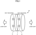
- FIG. 1 is a perspective view illustrating a structure of a joined body 10 according to Embodiment 1.
- the joined body 10 includes an optical material 11 (first material) and a pair of cooling materials 12 (second materials) each of which is joined to each of the two ends of the optical material 11.
- Each of the optical material 11 and the cooling material 12 is formed of a material capable of transmitting light and, more specifically, is formed of a transparent material.
- the optical material 11 and the cooling material 12 are joined to each other without involving means for bonding materials, such as an adhesive.
- “Joining” means binding materials in contact with each other by diffusive entry of atoms from at least one of the materials to the other material. "Joining” does not include a case of binding materials by involving means for bonding the materials, such as an adhesive. At a joining interface in the joined body 10, part of atoms of the optical material 11 diffusively enter the cooling material 12, or part of atoms of the cooling material 12 diffusively enter the optical material 11. Consequently, the optical material 11 is firmly joined to the cooling material 12.
- joining also includes a case of, when atoms diffusively enter from one material to another material, an intermediate layer originating in the atoms constituting the materials being formed between the materials in contact with each other and the materials being bound through the intermediate layer. Further, it is also included that a case of placing an intermediate layer (such as a SiO 2 layer) causing diffusion and entry of atoms with one material and the other material between the one material and the other material, and binding the materials through the intermediate layer.
- an intermediate layer such as a SiO 2 layer
- each of the optical material 11 and the cooling material 12 is disk-shaped and is formed at the same outer diameter.
- the outer diameter of the joined body 10 may be approximately 10 mm or greater, may be, for example, approximately 0.5 mm to approximately 300 mm, and may preferably be approximately 10 mm to approximately 100 mm. Further, when defined by an area, for example, the size of the joined body 10 may be in a range from approximately 100 mm 2 to 1.0 m 2 .
- the optical material 11 is a laser medium in a laser oscillator.
- the laser medium amplifies light by absorbing light emitted from a pumping light source and causing induced emission.
- the laser medium is formed of a phosphor absorbing light at a specific wavelength and emitting light at another wavelength based on the specific wavelength.
- the optical material 11 is a polycrystal such as yttrium aluminum garnet (YAG) or Nd:YAG.
- Nd:YAG is in a same material type relation with YAG and is acquired by doping YAG with neodymium (Nd) and replacing part of yttrium (Y) with neodymium.
- Polycrystals such as YAG and Nd:YAG have excellent light absorbance. Therefore, increasing in output power of a laser oscillator can be achieved by using the polycrystals.
- the thickness of the optical material 11 is approximately 0.1 mm to approximately 100 mm.
- a polycrystal constituting the optical material 11 may be a material acquired by doping a basic material such as YAG, lutetium aluminum garnet (LuAG), Y 2 O 3 , L u2 O 3 , or CaF 2 with a rare-earth ion such as Ce, Pr, Nd, Sm, Eu, Tb, Dy, Ho, Er, Tm, or Yb.
- the basic material may be co-doped with a plurality of types of rare-earth ions.
- the cooling material 12 is a material capable of transmitting light, transfers heat generated in the optical material 11, and emits the heat to the outside.
- the cooling material 12 is formed of a material having a thermal conductivity higher than that of the optical material 11.
- the cooling material 12 is a monocrystal such as sapphire, aluminum nitride, gallium nitride, silicon carbide, or diamond.
- the thickness of the cooling material 12 is approximately 0.1 mm to approximately 100 mm.
- Sapphire has a property of having a higher damage threshold value compared with YAG.
- the damage threshold value is a threshold value of an amount of energy per unit area that can be supplied without damaging the material.
- a degree of diffusive entry of atoms at the joining interface in the joined body 10 is evaluated by an index called a "diffusive entry length" including a case of providing an intermediate layer between one material and the other material.
- a diffusive entry length is expressed by ⁇ Dt in a case of fitting, by Equation (1) below, a one-dimensional concentration distribution of atoms acquired when atoms contained in one material of the joined body 10 diffusively enter the other material.
- C x denotes concentration (in any units) of the atoms at a distance x
- x denotes a distance (m)
- x 0 denotes a distance (m) of a position where the concentration of the atoms is C 0 /2
- D denotes a diffusion coefficient (m 2 /sec)
- t denotes time (sec).
- the diffusive entry length of atoms of the joined body 10 is set in such a degree that the optical material 11 and the cooling material 12 are firmly joined together. At the same time, transparency and absorbency of the optical material 11 and the cooling material 12 are not affected.
- a diffusive entry length of atoms of the joined body 10 satisfying the condition described above is in a range from approximately 1.0 nm to approximately 100 nm or may be in a range from approximately 1.0 nm to approximately 10 nm.
- the central part of the optical material 11 reaches a high temperature, and therefore a temperature gradient is generated in a radial direction.
- a temperature gradient generated in the optical material 11 causes thermal expansion, a refractive index gradient, and the like.
- the temperature gradient causes degradation in beam quality and decrease in laser output.
- the joined body 10 is formed in such a way that the cooling materials 12 arranged in an oscillation direction of laser light sandwich the optical material 11, and therefore heat generated in the central part of the optical material 11 can be efficiently discharged.
- the cooling materials 12 are joined to both ends of the optical material 11 in the joined body 10 according to Embodiment 1, and therefore thermal resistance at the interface is lower compared with a case of bonding the two. Accordingly, heat generated in the optical material 11 can be conducted to the cooling material 12 and can be efficiently discharged to the outside.
- optical material 11 is joined to the cooling material 12 without involving the air, an adhesive, or the like in the joined body 10 according to Embodiment 1, and therefore sufficient optical quality can be acquired by suppressing Fresnel loss and intensity can be sufficiently secured.
- the optical material 11 is formed of a polycrystal
- the cooling material 12 is formed of a monocrystal in the joined body 10 according to Embodiment 1. Accordingly, even though the optical material 11 is formed of a polycrystal, damage to the joined body 10 can be prevented by sandwiching the optical material 11 by the cooling materials 12 formed of monocrystals.
- FIG. 2 is a diagram illustrating a structure of a laser oscillator 1 according to Embodiment 1.
- the laser oscillator 1 includes a joined body 10 including a laser medium, a resonator 20 placed in such a way as to sandwich the joined body 10, and pumping light sources 30 supplying pumping light to the joined body 10 and causing laser light to resonate in the resonator 20.
- the resonator 20 includes a reflecting mirror 21 totally reflecting light and an output mirror 22 capable of taking out part of light to the outside.
- the reflecting mirror 21 and the output mirror 22 are placed in such a way as to face each other with the joined body 10 in between.
- the pumping light sources 30 are placed in such a way as to face each other in a radial direction of the joined body 10 with the joined body 10 in between.
- the laser oscillator 1 amplifies laser light by induced emission every time the laser light passes through the joined body 10, by causing the laser light to repeatedly reflect between the reflecting mirror 21 and the output mirror 22, and emits part of the laser light through the output mirror 22.
- the laser oscillator 1 includes the joined body 10 and therefore can efficiently discharge heat generated in the central part of the optical material 11 in a propagation direction of laser light through the cooling material 12. Accordingly, heat can be effectively discharged even when the laser oscillator 1 is downsized, and therefore a small-sized laser device such as a microchip laser can be provided.
- PECS pulsed electric current sintering
- PECS causes diffusion of atoms between the materials and joins materials to be joined to each other by simultaneously performing pressurization and heating of the materials.
- PECS causes a punch and a die for pressurizing materials to generate heat and heats the materials by heat conduction of the punch and the die. Therefore PECS allows more rapid heating compared with a case of using an electric furnace or the like. Accordingly, structural change, such as grain growth, occurring due to exposing materials in a high-temperature environment for a long time can be suppressed.
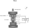
- FIG. 3 is a diagram illustrating a structure of a manufacturing device 100 for manufacturing the joined body 10.
- the manufacturing device 100 is a device being installed in a vacuum or in an inert gas and manufacturing the joined body 10 by pressurizing materials to be joined and heating the materials by supplying pulse current to the materials.
- the manufacturing device 100 includes a pair of vertically placed spacers 110, a pair of punches 120 pressurizing materials to be joined to each other, each punch being fixed at the end of a spacer 110, a die 130 internally housing the pair of punches 120 and the materials, and a pulse current source 140 supplying pulse current from one spacer 110 to the other spacer 110.
- the spacer 110 holds the punches 120 and presses the materials from a vertical direction through the punches 120. Further, each spacer 110 is electrically connected to the pulse current source 140 and supplies pulse current from one punch 120 to the other punch 120.
- the lower spacer 110 is installed on a base of the manufacturing device 100.
- the upper spacer 110 is fixed to a moving mechanism (unillustrated) of the manufacturing device 100 and is formed in such a way as to be movable in a vertical direction relative to the lower spacer 110.
- the punch 120 is a member being in direct contact with a material and pressing the material and at the same time supplying pulse current from the spacer 110 to the material.
- the punch 120 is a cylindrical member and is formed of an electroconductive material such as graphite.
- the diameter of the punch 120 corresponds to the diameter of the joined body 10 and, for example, is approximately 0.5 mm to approximately 300 mm and is preferably approximately 10 mm to approximately 100 mm.
- the die 130 is a member internally housing materials and supplying pulse current supplied from the punch 120 to the outer peripheral surface of the materials.
- the die 130 is a tubular member including a through hole being capable of housing materials and allowing the punches 120 to be inserted.
- the die 130 is formed of an electroconductive material such as graphite.
- the inside diameter of the die 130 is set in such a way that the outer peripheral surface of the materials and the outer peripheral surface of the punch 120 come in contact with the inner peripheral surface of the die 130.
- FIG. 4 is a flowchart illustrating a flow of a manufacturing process of the joined body 10 manufactured by use of the manufacturing device 100. A flow of the manufacturing process of the joined body 10 will be described below with reference to FIG. 4 .
- an optical material 11 and cooling materials 12 are integrally assembled (Step S1).
- the optical material 11 and the cooling materials 12 may be integrally assembled by placing a cooling material 12 at each of two ends of the optical material 11 and applying an adhesive to the outer peripheral surface of a part where the optical material 11 is in contact with the cooling material 12. Further, the two may be bonded by bonding surfaces of the optical material 11 and the cooling materials 12 together in an activated state.
- the integrally assembled optical material 11 and the cooling materials 12 are formed in such a way as to have predetermined transmission wave surface precision.
- the transmission wave surface precision is approximately ⁇ or less, is preferably approximately ⁇ /2 or less, and is more preferably approximately ⁇ /4 or less.
- the lower limit of the transmission wave surface precision may be approximately ⁇ /8 or less.
- Step S2 the materials assembled in Step S1 are placed at a predetermined position in the manufacturing device 100 (Step S2). More specifically, first, the materials are placed inside the through hole of the die 130 in such a way that a direction in which the optical material 11 and the cooling material 12 are laid on top of each other matches an axial direction of the through hole of the die 130. Subsequently, the materials are placed in the manufacturing device 100 by inserting the pair of punches 120 into the through hole of the die 130.
- the materials are pressurized at a predetermined pressure by moving the upper spacer 110 downward (Step S3).
- the materials are pressurized in the direction in which the optical material 11 and the cooling material 12 are laid on top of each other.
- the predetermined pressure is in a range from approximately 1.0 MPa to approximately 10 GPa, is preferably in a range from approximately 5.0 MPa to approximately 1.0 GPa, and is more preferably in a range from approximately 5.0 MPa to approximately 0.1 GPa.
- Step S4 the materials in a pressurized state are heated to a predetermined temperature by supplying pulse current to the materials. More specifically, the punches 120 generate heat by supplying pulse current to the punches 120, the heat is conducted to the materials, and the materials are quickly heated. Consequently, As a reason for that the temperature of the optical material 11 and the cooling material 12 in the pressurized state rises, diffusion of atoms occurs at the joining interface, and therefore joining of the optical material 11 and the cooling material 12 progresses.
- the manufacturing device 100 can raise the temperature of the materials at 500°C/min.
- the predetermined temperature and the temperature rise rate are set in consideration of types, shapes, sizes, a state of the contact surface, and the like of the optical material 11 and the cooling material 12.
- the predetermined temperature is in a range from approximately 900°C to approximately 1500°C, is preferably in a range from approximately 1000°C to approximately 1400°C, and is more preferably in a range from approximately 1100°C to approximately 1200°C.
- the state of the materials being pressurized at the predetermined pressure and being heated at the predetermined temperature is continued for a predetermined time.
- the predetermined time is set in such a way that a desired diffusive entry length is acquired, in consideration of the types, the shapes, the sizes, the state of the contact surface, and the like of the optical material 11 and the cooling material 12.
- the predetermined time is in a range from approximately 5 minutes to approximately 20 hours and is preferably in a range from approximately 1 hour to approximately 2 hours.
- Step S5 whether the predetermined time has elapsed since a point of the materials reaching the predetermined temperature is determined.
- the pressure on the materials is gradually decreased and, at the same time, the temperature of the materials is gradually decreased (Step S6). It is preferable in Step S6 to gradually cool and gradually decompress the materials at a predetermined temperature fall rate and at a predetermined decompression rate.
- the temperature fall rate and the decompression rate are set in consideration of the types, the shapes, the sizes, the state of the contact surface, and the like of the optical material 11 and the cooling material 12.
- Step S5 when the predetermined time has not elapsed since the point of the materials reaching the predetermined temperature (Step S5; No), the pressurization of the material at the predetermined pressure and the heating of the materials at the predetermined temperature are continued until the predetermined period elapses.
- Step S6 the materials cooled in Step S6 are removed from the manufacturing device 100 (Step S7), and by performing optical polishing on the reflection surface of the materials (Step S8), the manufacture of the joined body 10 ends.
- Step S7 the materials cooled in Step S6 are removed from the manufacturing device 100
- Step S8 the materials cooled in Step S6 are removed from the manufacturing device 100
- Step S8 the materials cooled in Step S6 are removed from the manufacturing device 100
- Step S8 by performing optical polishing on the reflection surface of the materials
- thermal diffusion joining method heats materials by use of an electric furnace or the like and therefore requires high-temperature heat treatment for a long time; and it is difficult to make a diffusive entry length of atoms at the joining interface approximately 10 ⁇ m or less.
- thermal expansion occurs in a clamp for pressurizing materials at a high temperature in the thermal diffusion joining method, and therefore it is difficult to control pressure actually applied to the materials.
- thermal expansion occurs in the materials themselves at a high temperature in the thermal diffusion joining method, and therefore it is difficult to join different types of materials with different thermal expansion coefficients to each other.
- the normal temperature joining method requires extremely high surface precision for joining interfaces to each other. More specifically, denoting a wavelength of laser light emitted from a laser interferometer used for measuring transmission wave surface precision by ⁇ , transmission wave surface precision required of materials is required to be approximately ⁇ /8 or less. It is difficult to form materials having a wide area with high surface precision, and therefore it is difficult to achieve upsizing of a joined body (such as approximately 100 mm 2 or greater) by the normal temperature joining method. Further, the normal temperature joining method does not heat materials, and therefore it is difficult to make a diffusive entry length at a joining interface approximately 1.0 nm or greater. Furthermore, the normal temperature joining method requires a high degree of vacuum, and therefore a manufacturing cost is high.
- the manufacturing method according to Embodiment 1 can perform heat treatment on materials in a short period of time by use of pulse current and therefore can easily join the materials together in a short period of time. Further, As a reason for that the manufacturing method according to Embodiment 1 uses pulse current for heating materials, thermal expansion does not occur in the punch 120 and the die 130, and the pressure applied to the materials can be accurately controlled even at a high temperature.
- the manufacturing method according to Embodiment 1 can control a diffusive entry length of atoms at a joining interface of materials to a desired range (such as from approximately 1.0 nm to approximately 10 ⁇ m) and can suppress structural change, such as grain growth, in a polycrystal under heat treatment. Moreover, the manufacturing method according to Embodiment 1 can achieve upsizing of the joined body 10 (such as an area of approximately 100 mm 2 or greater) since materials can be joined to each other even when transmission wave surface precision at a joining interface is approximately ⁇ or less and can suppress a manufacturing cost since a high degree of vacuum is not required.
- a desired range such as from approximately 1.0 nm to approximately 10 ⁇ m
- the joined body 10 according to Embodiment 2 differs from the joined body 10 according to Embodiment 1 in joining a saturable absorber 13 (second material) to an optical material 11 (first material).
- the joined body 10 includes the optical material 11 being a laser medium and the saturable absorber 13 joined to one surface of the optical material 11.
- the saturable absorber 13 acts as an absorber for low-intensity incident light and acts as a transparent body for high-intensity incident light by saturation of an ability as an absorber.
- the saturable absorber 13 is formed of YAG doped with Cr (Cr:YAG).
- the laser oscillator 1 includes a reflecting mirror 21 being placed on the optical material 11 side of the joined body 10 and totally reflects laser light, and an output mirror 22 being placed on the opposite side of the reflecting mirror 21 with the joined body 10 in between and partially reflecting laser light.
- the reflecting mirror 21 and the output mirror 22 constitute a resonator 20 resonating laser light inductively emitted by the joined body 10.
- a pulse width (time duration) of laser light in the laser oscillator 1 becomes shorter, and, for example, a light pulse with a width of the order of picoseconds to nanoseconds is emitted.
- the laser oscillator 1 includes the saturable absorber 13 joined to the optical material 11. Accordingly, the laser oscillator 1 can provide sufficient optical quality by suppressing Fresnel loss and can achieve pulse shortening of laser light.
- the joined body 10 according to Embodiment 3 differs from the joined bodies 10 according to Embodiments 1 and 2 in joining a spontaneous emission absorber 14 (second material) in such a way that the spontaneous emission absorber 14 surrounds the outer periphery of an optical material 11 (first material).
- the joined body 10 includes the optical material 11 being a laser medium and the spontaneous emission absorber 14 being joined around the optical material 11 and absorbing light from the laser medium.
- the spontaneous emission absorber 14 is formed of Sm:YAG or Cr:YAG.
- ASE amplified spontaneous emission
- ASE is light generated by spontaneous emission generated in a laser medium propagating through the laser medium.
- ASE may cause resonance (parasitic oscillation) in a direction other than an oscillation direction of laser light.
- the spontaneous emission absorber 14 is joined in such a way as to surround the outer periphery of the optical material 11 in the joined body 10 according to Embodiment 3; and therefore spontaneous emission is absorbed by the spontaneous emission absorber 14, and, as a result, ASE and parasitic oscillation are suppressed. Further, the spontaneous emission absorber 14 itself is a non-heat-generating material and therefore can absorb heat generated by the optical material 11 and discharge the heat to the outside.
- the laser oscillator 1 according to Embodiment 3 includes the spontaneous emission absorber 14 joined in such a way as to surround the outer periphery of the optical material 11. Accordingly, even when ASE is generated and light enters the spontaneous emission absorber 14 from the optical material 11, parasitic oscillation can be suppressed, and at the same time, the optical material 11 can be cooled. As a result, decrease in laser output in the laser oscillator 1 can be suppressed.
- the laser amplifier 2 is a device amplifying laser light entering from the outside with a laser medium and emitting the amplified light to the outside. Unlike the laser oscillators 1 according to Embodiments 1 to 3, the laser amplifier 2 does not include a resonator 20.
- the laser amplifier 2 includes the joined body 10, a pumping light source 30, and an amplified light source 40.
- the pumping light source 30 emits light to the joined body 10 in such a way as to pump the joined body 10.
- the amplified light source 40 introduces light to the joined body 10 in such a way that the light is amplified by the joined body 10.
- the light emitted from the amplified light source 40 is amplified by an optical material 11 in the joined body 10 pumped by the pumping light source 30 and is emitted from the joined body 10.
- cooling materials 12 are joined to both sides of the optical material 11, and therefore heat generated in the central part of the optical material 11 can be efficiently discharged in a propagation direction of the laser light through the cooling material 12.
- the laser amplifier 2 includes the joined body 10 in which the optical material 11 is joined to the cooling materials 12 and therefore can effectively cool the optical material 11 pumped by the pumping light source 30. Accordingly, heat can be effectively discharged even when the laser amplifier 2 is downsized, and thus downsizing of the laser amplifier 2 can be achieved.
- a 1% Nd:YAG polycrystal and a sapphire monocrystal were worked into disk shapes having the same outer diameter.
- the 1% Nd:YAG polycrystal is acquired by doping YAG with 1% of neodymium.
- a bonded body was acquired by laying the worked Nd:YAG polycrystal and sapphire monocrystal on top of each other and applying an adhesive to the outer peripheral part.
- FIG. 8 indicates conditions for temperature and pressure in PECS for each sample of a joined body.
- a sample of a joined body (may be hereinafter referred to as an Nd:YAG/sapphire joined body) was produced by processing a bonded body integrated by an adhesive, in accordance with a condition in FIG. 8 .
- success or failure of joining was determined for each produced sample by confirming existence of an interference fringe and measuring a transmission spectrum for each sample.
- FIG. 9 is a graph for illustrating success or failure of joining in the samples produced under the conditions in FIG. 8 .
- the vertical axis of FIG. 9 represents pressure (MPa) in PECS, and the horizontal axis represents temperature (°C) in PECS.
- a symbol ⁇ in FIG. 9 represents a sample 1 (1100°C, 36 MPa), a symbol ⁇ represents a sample 2 (1200°C, 12 MPa), a symbol of "double circle” represents a sample 3 (1100°C, 62 MPa), and a symbol o represents a sample 4 (1200°C, 36 MPa).
- An interference fringe was observed in the entire sample 1. Further, an interference fringe was observed on the periphery of the sample 2 and the sample was slightly blackish. On the other hand, an interference fringe did not exist at all in the sample 3, and the most excellent result was exhibited. Further, while an interference fringe did not exist at all in the sample 4, the sample was slightly blackish.
- the bonded body is acquired by laying a sapphire monocrystal and an Nd:YAG polycrystal on top of each other and applying an adhesive to the outer peripheral surface
- the joined body is an Nd:YAG/sapphire joined body acquired under the condition of 1100°C and 62 MPa providing the most excellent result in Example 1.
- a transmission spectrum indicates a transmissivity of a sample for each wavelength of incident light entering the sample; and a transmissivity is a ratio of incident light at a specific wavelength transmitted through the sample. Part of incident light entering a sample is reflected from the surface of the sample, the joining interface of materials, and the like. Accordingly, intensity of transmitted light transmitted through the sample decreases compared with that of the incident light entering the sample.
- a transmission spectrum of each sample was generated by measuring a radiant emittance of transmitted light transmitted through each sample and calculating a ratio between radiant emittances of transmitted light and incident light for each wavelength of incident light. Note that a radiant emittance is an emission flux per unit area emitted from an emitter.
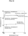
- FIG. 10 is a graph illustrating transmission spectra in an Nd:YAG polycrystal, a bonded body, and a joined body.
- the vertical axis of FIG. 10 represents a transmissivity (%), and the horizontal axis represents a wavelength (nm) of incident light.
- a solid line in FIG. 10 represents an actually measured transmissivity, and a dotted line represents a theoretical value of transmissivity.
- a transmissivity of the joined body had a value higher than that of the bonded body by approximately 13% and a value higher than that of the Nd:YAG polycrystal.
- the reason the transmissivity of the joined body was higher than the transmissivities of the bonded body and the Nd:YAG polycrystal is that Fresnel loss was suppressed by a sapphire monocrystal being joined to the Nd:YAG polycrystal.
- the transmissivity (experimental value) of the joined body was 84.1%, whereas the transmissivity (experimental value) of the bonded body was 71.6%, and the transmissivity (experimental value) of the Nd:YAG polycrystal was 83.9%. Since the transmissivity (theoretical value) of the joined body was 84.7%, the transmissivity (theoretical value) of the bonded body was 71.8%, and the transmissivity (theoretical value) of the Nd:YAG polycrystal was 83.9%, the experimental result on transmission spectra is confirmed to be valid.
- FIG. 11 is a diagram illustrating an SEM image including the joining interface in the joined body.
- the left side of FIG. 11 represents an Nd:YAG polycrystal, and the right side represents a sapphire monocrystal.
- FIG. 11 it is confirmed that there is no space at the joining interface between the sapphire monocrystal and the Nd:YAG polycrystal, and the two are excellently joined together even at a micro level.
- FIG. 12 is a graph illustrating the result of the elementary analysis in the joined body.
- the vertical axis of FIG. 12 represents intensity (in any units) of characteristic X-rays, and the horizontal axis represents a distance (nm) from the surface of the Nd:YAG polycrystal.
- the left side of FIG. 12 represents an Nd:YAG region, the central part represents a region of the interface between Nd:YAG and sapphire, and the right side represents a sapphire monocrystal region.
- a state of a solid line indicating intensity of characteristic X-rays related to yttrium (Y) sloping from upper left toward lower right in the interface region is observed. The above indicates that yttrium contained in the Nd:YAG polycrystal diffusively entered the sapphire monocrystal.
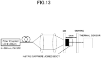
- FIG. 13 illustrates an example of the laser oscillation experimental system incorporating the joined body.
- the experimental system includes a pumping semiconductor laser (LD), an optical fiber, a lens system, an Nd:YAG/sapphire joined body, a dichroic mirror (DM), an output mirror (OC), and a thermal sensor.
- the LD emits continuous light (CW) having a wavelength ⁇ of 808 nm and a laser output of 18 W.
- the optical fiber has a diameter of approximately 100 ⁇ m and transmits laser light from the LD toward the lens system.
- the lens system causes laser light supplied from the optical fiber to converge toward Nd:YAG.
- the thermal sensor receives laser light emitted from the OC and measures laser output.
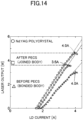
- FIG. 14 is a graph illustrating an input-output characteristic of the laser oscillation experimental system.
- the vertical axis of FIG. 14 represents laser output (W) output from the experimental system, and the horizontal axis represents current (A) applied to the LD.
- a symbol o in FIG. 14 represents a measured value when the Nd:YAG polycrystal is used, a symbol ⁇ represents a measured value when the bonded body is used, and a symbol ⁇ represents a measured value when the joined body is used.
- the laser output when the Nd:YAG polycrystal was incorporated into the laser oscillation experimental system was 3.56 W, whereas the laser output when the joined body was incorporated into the laser oscillation experimental system was 4.62 W. Incorporation of the joined body into the laser oscillation experimental system increased laser output by approximately 30% compared with the case of the Nd:YAG polycrystal.
- the maximum pump current when the Nd:YAG polycrystal was used was 3.6 A
- the maximum pump current when the joined body was used was 4.0 A
- the maximum pump current when the bonded body was used was also 4.0 A. The above indicates that the maximum pump current increased due to a conduction cooling effect by sapphire contained in the joined body and the bonded body. It is further understood that when the joined body was used in the laser oscillation system, laser output also increased with increase in the maximum pump current.
- a solid line in FIG. 15 represents a one-dimensional concentration distribution of the yttrium element, and a broken line is acquired by fitting the one-dimensional concentration distribution of the yttrium element represented by the solid line by Equation (1).
- a diffusive entry length is defined by ⁇ Dt in Equation (1), and therefore the diffusive entry length ⁇ Dt in FIG. 15 is 1.6 nm.
- a diffusive entry length of an yttrium element in an Nd: YAG/sapphire joined body is roughly 1.0 nm or greater. Further, calculation of a diffusive entry length using Equation (1) is applicable not only to the case of an Nd:YAG/sapphire joined body but also to a case of calculating a diffusive entry length of another joined body.
- the same-type materials may be joined together to form a joined body 10.
- the same-type materials include a material acquired by doping a basic material with an active element, such as Nd:YAG for YAG.
- the cooling material 12 may be joined to one surface of the optical material 11, or the cooling material 12 may be joined to the outer peripheral surface of the optical material 11. Further, the cooling material 12 may be joined to the front of the optical material 11.
- optical material 11 and the cooling material 12 are disk shapes having the same outer diameter in the aforementioned embodiments, the present disclosure is not limited thereto.
- the optical material 11 and the cooling material 12 may be disk-shaped members having different outer diameters.
- the optical material 11 and the cooling material 12 may be rectangular or polygonal plate-shaped members.
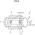
- the optical material 11 and the cooling material 12 may have shapes different from each other; and for example, a plurality of elongated cylindrical-shaped optical materials 11 may be joined to a pair of cooling materials 12 in such a way as to be sandwiched by the cooling materials 12, as illustrated in FIG. 16 .
- optical material 11 is formed of a polycrystal
- the cooling material 12 is formed of a monocrystal in the aforementioned embodiments
- the present disclosure is not limited thereto.
- Each of the optical material 11 and the cooling material 12 may be any one of a monocrystal, a polycrystal, and a glass body as long as the material is capable of transmitting light.
- the cooling material 12 may be formed of a polycrystal such as aluminum nitride.
- the joined body 10 is cylindrically formed in the aforementioned embodiments, the present disclosure is not limited thereto.
- the joined body 10 may be cut in such a way that an end has Brewster's angle.
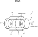
- the resonator 20 in the laser oscillator 1 includes the reflecting mirror 21 and the output mirror 22, and the pumping light sources 30 in the laser oscillator 1 and the laser amplifier 2 cause side pumping in the aforementioned embodiments
- the present disclosure is not limited thereto.
- anti-reflection (AR) coating or high-reflection (HR) coating may be applied to both ends of the joined body 10 in the laser oscillator 1, and a resonator may be formed in the joined body 10.
- the pumping light sources 30 in the laser oscillator 1 and the laser amplifier 2 may be placed in such a way as to cause end pumping.
- optical material 11 and the cooling material 12 are combined and then are installed in the manufacturing device 100 in the aforementioned embodiments, the present disclosure is not limited thereto.
- the optical material 11 and the cooling material 12 may be installed at predetermined positions in the manufacturing device 100 in such a way as to be laid on top of each other in order, without being combined in advance.
- pressure and temperature of the optical material 11 and the cooling material 12 are gradually decreased after a predetermined time elapses in the aforementioned embodiments, the present disclosure is not limited thereto.
- pressurization and heating of the optical material 11 and the cooling material 12 may be stopped after a predetermined time elapses.
- the materials may be cooled by natural air cooling, or the materials may be cooled by blowing air.
- the optical material 11 is a laser medium in the aforementioned embodiments, the present disclosure is not limited thereto.
- the optical material 11 may be a magneto-optical material.
- the magneto-optical material may be a material rotating a polarization plane by the Faraday effect for use in an optical isolator and a Faraday rotator.
- the magneto-optical material may be a material elliptically polarizing reflected light by the magneto-optical Kerr effect for use in polarizer glass and the like.
- the optical material 11 may be a phosphor changing a color tone of laser light emitted from the laser oscillator. After entering an excited state by absorbing energy of light from the outside, the phosphor emits light having different energy in a process of returning to a ground state.
- the phosphor may be doped with an active element. The phosphor may be used for adjusting a color tone of a light emitting diode (LED) lamp.
- LED light emitting diode
- the manufacturing device 100 is operated in a vacuum in the aforementioned embodiments, the present disclosure is not limited thereto.
- the manufacturing device 100 may be operated in an atmosphere of an inert gas such as argon and nitrogen.
- the spontaneous emission absorber 14 is used in aforementioned Embodiment 3, the present disclosure is not limited thereto.
- a scatterer scattering oscillation light around the optical material 11 may be joined in order to suppress parasitic oscillation.
- the joined body 10 may be applied to a laser amplifier, an optical isolator, and a Faraday rotator.
- the joined body, the laser oscillator, the laser amplifier, and the joined body manufacturing method according to the present disclosure provide sufficient optical quality even when materials capable of transmitting light are combined and therefore are useful.
Landscapes
- Chemical & Material Sciences (AREA)
- Engineering & Computer Science (AREA)
- Crystallography & Structural Chemistry (AREA)
- Organic Chemistry (AREA)
- Materials Engineering (AREA)
- Metallurgy (AREA)
- Physics & Mathematics (AREA)
- Electromagnetism (AREA)
- Inorganic Chemistry (AREA)
- Optics & Photonics (AREA)
- Plasma & Fusion (AREA)
- Ceramic Engineering (AREA)
- Thermal Sciences (AREA)
- Mechanical Engineering (AREA)
- Lasers (AREA)
- Crystals, And After-Treatments Of Crystals (AREA)
Claims (11)
- Verbundener Körper (10), umfassend ein erstes Material (11) und ein zweites Material (12, 13), die in der Lage sind, Licht zu übertragen, und miteinander verbunden sind,wobei an einer Verbindungsgrenze zwischen dem ersten Material (11) und dem zweiten Material (12, 13) der verbundene Körper (10) in der Lage ist, Licht zu übertragen, und weiterhin Anteile von Atomen, die in jedem der Materialien (11) enthalten sind, in einem solchen Ausmaß in das andere der Materialien (12, 13) diffundieren, dass in dem verbundenen Körper (10) kein Interferenzstreifen erzeugt wird,
dadurch gekennzeichnet, dasseine Diffusionseintrittslänge der Atome des verbundenen Körpers (10) in einem Bereich von etwa 1 nm bis etwa 100 nm liegt. - Verbundener Körper nach Anspruch 1, wobei,
unter der Annahme, dass eine Wellenlänge λ von Laserlicht, das von einem Laserinterferometer emittiert wird, das zur Messung der Transmissionswellenoberflächengenauigkeit verwendet wird, 633 nm beträgt, die Transmissionswellenoberflächengenauigkeit des ersten Materials (11) und des zweiten Materials (12, 13) ungefähr λ oder weniger beträgt. - Verbundener Körper nach einem der Ansprüche 1 bis 2, wobei
das erste Material (11) ein Polykristall ist und das zweite Material (12, 13) ein Einkristall ist. - Verbundener Körper nach Anspruch 3, wobeider Polykristall YAG oder mit einem Seltenerdion dotierter YAG ist, undder Einkristall Saphir, Aluminiumnitrid, Galliumnitrid, Siliziumkarbid oder Diamant ist.
- Verbundener Körper nach einem der Ansprüche 1 bis 4, wobei
das erste Material (11) ein Leuchtstoff oder ein magneto-optisches Material ist und das zweite Material (12, 13) ein Material ist, das eine höhere Wärmeleitfähigkeit als das erste Material (11) aufweist. - Laseroszillator (1), aufweisend:den verbundenen Körper (10) nach einem der Ansprüche 1 bis 5;einen Resonator (20), der so angeordnet ist, dass er den verbundenen Körper (10) sandwichartig einschließt und Licht, das von dem verbundenen Körper (10) gepumpt wird, in Resonanz bringt; undeine Pumplichtquelle (30), die Licht zu dem verbundenen Körper (10) derart emittiert, dass der verbundene Körper (10) gepumpt wird.
- Laserverstärker (2), aufweisend:den verbundenen Körper (10) nach einem der Ansprüche 1 bis 5;eine Pumplichtquelle (30), die Licht auf den verbundenen Körper (10) derart emittiert, dass der verbundene Körper (10) gepumpt wird; undeine Verstärkerlichtquelle, die Licht zu dem verbundenen Körper (10) derart einführt, dass das Licht durch den verbundenen Körper (10) verstärkt wird.
- Verfahren zur Herstellung eines verbundenen Körpers (10), der ein erstes Material (11) und ein zweites Material (12, 13) aufweist, die in der Lage sind, Licht zu übertragen, und miteinander verbunden sind, wobei Anteile von Atomen, die in jedem der Materialien (11) enthalten sind, in einem solchen Ausmaß in das andere der Materialien (12, 13) diffundieren, dass in dem verbundenen Körper (10) kein Interferenzstreifen erzeugt wird, wobei das Verfahren zur Herstellung des verbundenen Körpers aufweisteinen Schritt des Übereinanderlegens des ersten Materials (11) und des zweiten Materials (12, 13);einen Schritt des Druckbeaufschlagens des ersten Materials (11) und des zweiten Materials (12, 13) bei einem vorbestimmten Druck derart, dass das erste Material (11) und das zweite Material (12, 13) eng miteinander verbunden werden;einen Schritt des Erwärmens des ersten Materials (11) und des zweiten Materials (12, 13) auf eine vorbestimmte Temperatur durch Zuführen von elektrischem Impulsstrom zu dem unter Druck stehenden ersten Material (11) und dem unter Druck stehenden zweiten Material (12, 13);einen Schritt des, für eine vorbestimmte Zeit, Aufrechterhaltens des auf das erste Material (11) und das zweite Material (12, 13) ausgeübten Drucks auf einem vorbestimmten Druck und Aufrechterhaltens der Temperatur des ersten Materials (11) und des zweiten Materials (12, 13) auf einer vorbestimmten Temperatur; undeinen Schritt der allmählichen Verringerung des auf das erste Material (11) und das zweite Material (12, 13) ausgeübten Drucks und der Temperatur des ersten Materials (11) und des zweiten Materials (12, 13), wobeieine Diffusionseintrittslänge der Atome des verbundenen Körpers (10) in einem Bereich von ungefähr 1 nm bis ungefähr 100 nm liegt.
- Verfahren zur Herstellung eines verbundenen Körpers nach Anspruch 8, wobei der vorbestimmte Druck in einem Bereich von etwa 1 MPa bis etwa 10 GPa liegt.
- Verfahren zur Herstellung eines verbundenen Körpers nach Anspruch 8 oder 9, wobei die vorbestimmte Temperatur in einem Bereich von etwa 900°C bis etwa 1500°C liegt.
- Verfahren zur Herstellung eines gefügten Körpers nach einem der Ansprüche 8 bis 10, wobei
die vorbestimmte Zeit in einem Bereich von etwa 5 Minuten bis etwa 20 Stunden liegt.
Applications Claiming Priority (2)
| Application Number | Priority Date | Filing Date | Title |
|---|---|---|---|
| JP2018083878 | 2018-04-25 | ||
| PCT/JP2019/017503 WO2019208658A1 (ja) | 2018-04-25 | 2019-04-24 | 接合体、レーザ発振器、レーザ増幅器及び接合体の製造方法 |
Publications (3)
| Publication Number | Publication Date |
|---|---|
| EP3787133A1 EP3787133A1 (de) | 2021-03-03 |
| EP3787133A4 EP3787133A4 (de) | 2022-01-26 |
| EP3787133B1 true EP3787133B1 (de) | 2024-10-23 |
Family
ID=68294684
Family Applications (1)
| Application Number | Title | Priority Date | Filing Date |
|---|---|---|---|
| EP19791851.9A Active EP3787133B1 (de) | 2018-04-25 | 2019-04-24 | Verbundener körper, laseroszillator, laserverstärker und verfahren zur herstellung eines verbundenen körpers |
Country Status (4)
| Country | Link |
|---|---|
| US (1) | US12142888B2 (de) |
| EP (1) | EP3787133B1 (de) |
| JP (1) | JP6933349B2 (de) |
| WO (1) | WO2019208658A1 (de) |
Families Citing this family (1)
| Publication number | Priority date | Publication date | Assignee | Title |
|---|---|---|---|---|
| US20230208105A1 (en) * | 2021-12-28 | 2023-06-29 | David C. Brown | Miniature single-longitudinal-mode diode-pumped solid-state lasers |
Family Cites Families (16)
| Publication number | Priority date | Publication date | Assignee | Title |
|---|---|---|---|---|
| US5441803A (en) * | 1988-08-30 | 1995-08-15 | Onyx Optics | Composites made from single crystal substances |
| US5846638A (en) * | 1988-08-30 | 1998-12-08 | Onyx Optics, Inc. | Composite optical and electro-optical devices |
| TW200301980A (en) * | 2002-01-10 | 2003-07-16 | Hrl Lab Llc | Diffusion bonded pump cavity |
| US20060182162A1 (en) | 2003-07-29 | 2006-08-17 | Takayuki Yanagisawa | Solid laser exciting module and laser oscillator |
| JP2005262244A (ja) * | 2004-03-17 | 2005-09-29 | Suwa Netsukogyo Kk | パルス通電による金属部材の接合方法 |
| JP2005327997A (ja) | 2004-05-17 | 2005-11-24 | Akio Ikesue | 複合レーザー素子及びその素子を用いたレーザー発振器 |
| US20050276300A1 (en) * | 2004-05-25 | 2005-12-15 | Nat'l Inst Of Info & Comm Tech Inc Admin Agency | Laser device using two laser media |
| US7630423B2 (en) * | 2005-04-12 | 2009-12-08 | Raytheon Company | Glaze soldered laser components and method of manufacturing |
| JP5374732B2 (ja) | 2009-05-22 | 2013-12-25 | コーア株式会社 | シャント抵抗器の製造方法 |
| JP2013041051A (ja) * | 2011-08-12 | 2013-02-28 | Gigaphoton Inc | 波長変換装置、固体レーザ装置およびレーザシステム |
| EP3007288B1 (de) | 2013-06-06 | 2021-07-21 | Mitsubishi Electric Corporation | Laservorrichtung mit wellenleitern |
| JP6343229B2 (ja) * | 2014-11-18 | 2018-06-13 | 浜松ホトニクス株式会社 | レーザ増幅装置、レーザ装置及びレーザ核融合炉 |
| JP2016157905A (ja) * | 2015-02-26 | 2016-09-01 | 日本碍子株式会社 | 光学部品 |
| JP2017220652A (ja) * | 2016-06-10 | 2017-12-14 | 大学共同利用機関法人自然科学研究機構 | レーザ装置とその製造方法 |
| JP2018083878A (ja) | 2016-11-22 | 2018-05-31 | 積水化学工業株式会社 | タッチパネル用層間充填材料及びタッチパネル積層体 |
| EP3557293A4 (de) | 2016-12-13 | 2020-08-05 | NGK Insulators, Ltd. | Optische komponente |
-
2019
- 2019-04-24 EP EP19791851.9A patent/EP3787133B1/de active Active
- 2019-04-24 WO PCT/JP2019/017503 patent/WO2019208658A1/ja not_active Ceased
- 2019-04-24 JP JP2020515541A patent/JP6933349B2/ja active Active
- 2019-04-24 US US17/050,433 patent/US12142888B2/en active Active
Also Published As
| Publication number | Publication date |
|---|---|
| EP3787133A1 (de) | 2021-03-03 |
| EP3787133A4 (de) | 2022-01-26 |
| JP6933349B2 (ja) | 2021-09-08 |
| US12142888B2 (en) | 2024-11-12 |
| US20210296840A1 (en) | 2021-09-23 |
| WO2019208658A1 (ja) | 2019-10-31 |
| JPWO2019208658A1 (ja) | 2021-08-05 |
Similar Documents
| Publication | Publication Date | Title |
|---|---|---|
| US10367324B2 (en) | Laser component | |
| Tsunekane et al. | Analytical and experimental studies on the characteristics of composite solid-state laser rods in diode-end-pumped geometry | |
| US5563899A (en) | Composite solid state lasers of improved efficiency and beam quality | |
| US9065241B2 (en) | Methods, systems, and apparatus for high energy optical-pulse amplification at high average power | |
| US9209598B1 (en) | Cooling system for high average power laser | |
| JP2019129252A (ja) | 光学素子の製造方法及び光学素子 | |
| EP0854551B1 (de) | Dreiniveau-Lasersystem | |
| WO2009120584A2 (en) | Laser with highly efficient gain medium | |
| US8682125B2 (en) | Method and system for edge cladding of laser gain media | |
| US12142888B2 (en) | Joined body, laser oscillator, laser amplifier, and joined body manufacturing method | |
| EP3852209B1 (de) | Optischer oszillator | |
| Li et al. | Measurement of output characteristics of Tm: YAG laser at 25–300 K | |
| Baiocco et al. | Overcoming the output power threshold of 400 mW with high-gain diode pumped Pr: LiLuF4 waveguide lasers | |
| Kurilchik et al. | Characterisation and laser performance of a Yb: LuAG double-clad planar waveguide grown by pulsed laser deposition | |
| Weichelt | Experimental investigations on power scaling of high-brightness cw ytterbium-doped thin-disk lasers | |
| CN113644533A (zh) | 一种钬激光增益介质及钬激光器 | |
| Peysokhan et al. | Laser cooling characterization of Yb-doped ZBLAN fiber as a platform for radiation balanced lasers | |
| Cellamare et al. | Preliminary design of a Tm: Lu2O3-based amplifier for J-scale ultra-short pulses at a kW average power | |
| Waeselmann et al. | Lasing in Nd3+-doped Sapphire | |
| Quan et al. | Growth, spectroscopic, and 2.7-μm Q-switched laser properties of Cr, Er: YAP crystal by xenon-lamp pumping | |
| WO2013019300A9 (en) | Laser design | |
| Mukhin et al. | One kilohertz cryogenic disk laser with high average power | |
| Berry | Versatile chromium-doped zinc selenide infrared laser sources | |
| Duarte | Transparent Polycrystalline Er and Er, Cr Co-doped Al2O3 as Potential Gain Media for Lasers with an Eye Safe, 1.5 μm Emission | |
| Brutus | Optical Seed Development For Yb-Fiber Laser |
Legal Events
| Date | Code | Title | Description |
|---|---|---|---|
| STAA | Information on the status of an ep patent application or granted ep patent |
Free format text: STATUS: THE INTERNATIONAL PUBLICATION HAS BEEN MADE |
|
| PUAI | Public reference made under article 153(3) epc to a published international application that has entered the european phase |
Free format text: ORIGINAL CODE: 0009012 |
|
| STAA | Information on the status of an ep patent application or granted ep patent |
Free format text: STATUS: REQUEST FOR EXAMINATION WAS MADE |
|
| 17P | Request for examination filed |
Effective date: 20201123 |
|
| AK | Designated contracting states |
Kind code of ref document: A1 Designated state(s): AL AT BE BG CH CY CZ DE DK EE ES FI FR GB GR HR HU IE IS IT LI LT LU LV MC MK MT NL NO PL PT RO RS SE SI SK SM TR |
|
| AX | Request for extension of the european patent |
Extension state: BA ME |
|
| RIN1 | Information on inventor provided before grant (corrected) |
Inventor name: YASUHARA RYO Inventor name: FURUSE HIROAKI Inventor name: KOIKE YUKI |
|
| DAV | Request for validation of the european patent (deleted) | ||
| DAX | Request for extension of the european patent (deleted) | ||
| A4 | Supplementary search report drawn up and despatched |
Effective date: 20220104 |
|
| RIC1 | Information provided on ipc code assigned before grant |
Ipc: B32B 1/00 20060101ALI20211221BHEP Ipc: H01S 3/0941 20060101ALI20211221BHEP Ipc: H01S 3/094 20060101ALI20211221BHEP Ipc: H01S 3/04 20060101ALI20211221BHEP Ipc: C30B 29/40 20060101ALI20211221BHEP Ipc: B32B 9/04 20060101ALI20211221BHEP Ipc: B32B 9/00 20060101ALI20211221BHEP Ipc: B32B 7/027 20190101ALI20211221BHEP Ipc: B23B 1/00 20060101ALI20211221BHEP Ipc: H01S 3/16 20060101ALI20211221BHEP Ipc: C09K 11/80 20060101ALI20211221BHEP Ipc: H01S 3/10 20060101ALI20211221BHEP Ipc: H01S 3/042 20060101ALI20211221BHEP Ipc: C30B 33/06 20060101ALI20211221BHEP Ipc: C30B 29/38 20060101ALI20211221BHEP Ipc: C30B 29/36 20060101ALI20211221BHEP Ipc: C30B 29/20 20060101ALI20211221BHEP Ipc: C30B 29/04 20060101ALI20211221BHEP Ipc: B32B 7/04 20190101ALI20211221BHEP Ipc: H01S 3/06 20060101AFI20211221BHEP |
|
| GRAP | Despatch of communication of intention to grant a patent |
Free format text: ORIGINAL CODE: EPIDOSNIGR1 |
|
| STAA | Information on the status of an ep patent application or granted ep patent |
Free format text: STATUS: GRANT OF PATENT IS INTENDED |
|
| INTG | Intention to grant announced |
Effective date: 20240513 |
|
| RIN1 | Information on inventor provided before grant (corrected) |
Inventor name: YASUHARA, RYO Inventor name: KOIKE, YUKI Inventor name: FURUSE, HIROAKI |
|
| RAP1 | Party data changed (applicant data changed or rights of an application transferred) |
Owner name: INTER-UNIVERSITY RESEARCH INSTITUTE CORPORATIONNATIONAL INSTITUTES OF NATURAL SCIENCES Owner name: NATIONAL INSTITUTE FOR MATERIALS SCIENCE |
|
| GRAS | Grant fee paid |
Free format text: ORIGINAL CODE: EPIDOSNIGR3 |
|
| GRAA | (expected) grant |
Free format text: ORIGINAL CODE: 0009210 |
|
| STAA | Information on the status of an ep patent application or granted ep patent |
Free format text: STATUS: THE PATENT HAS BEEN GRANTED |
|
| AK | Designated contracting states |
Kind code of ref document: B1 Designated state(s): AL AT BE BG CH CY CZ DE DK EE ES FI FR GB GR HR HU IE IS IT LI LT LU LV MC MK MT NL NO PL PT RO RS SE SI SK SM TR |
|
| REG | Reference to a national code |
Ref country code: GB Ref legal event code: FG4D |
|
| REG | Reference to a national code |
Ref country code: CH Ref legal event code: EP |
|
| REG | Reference to a national code |
Ref country code: DE Ref legal event code: R096 Ref document number: 602019060838 Country of ref document: DE |
|
| REG | Reference to a national code |
Ref country code: IE Ref legal event code: FG4D |
|
| REG | Reference to a national code |
Ref country code: LT Ref legal event code: MG9D |
|
| REG | Reference to a national code |
Ref country code: NL Ref legal event code: MP Effective date: 20241023 |
|
| REG | Reference to a national code |
Ref country code: AT Ref legal event code: MK05 Ref document number: 1735627 Country of ref document: AT Kind code of ref document: T Effective date: 20241023 |
|
| PG25 | Lapsed in a contracting state [announced via postgrant information from national office to epo] |
Ref country code: NL Free format text: LAPSE BECAUSE OF FAILURE TO SUBMIT A TRANSLATION OF THE DESCRIPTION OR TO PAY THE FEE WITHIN THE PRESCRIBED TIME-LIMIT Effective date: 20241023 |
|
| PG25 | Lapsed in a contracting state [announced via postgrant information from national office to epo] |
Ref country code: NL Free format text: LAPSE BECAUSE OF FAILURE TO SUBMIT A TRANSLATION OF THE DESCRIPTION OR TO PAY THE FEE WITHIN THE PRESCRIBED TIME-LIMIT Effective date: 20241023 |
|
| PG25 | Lapsed in a contracting state [announced via postgrant information from national office to epo] |
Ref country code: PT Free format text: LAPSE BECAUSE OF FAILURE TO SUBMIT A TRANSLATION OF THE DESCRIPTION OR TO PAY THE FEE WITHIN THE PRESCRIBED TIME-LIMIT Effective date: 20250224 Ref country code: IS Free format text: LAPSE BECAUSE OF FAILURE TO SUBMIT A TRANSLATION OF THE DESCRIPTION OR TO PAY THE FEE WITHIN THE PRESCRIBED TIME-LIMIT Effective date: 20250223 Ref country code: HR Free format text: LAPSE BECAUSE OF FAILURE TO SUBMIT A TRANSLATION OF THE DESCRIPTION OR TO PAY THE FEE WITHIN THE PRESCRIBED TIME-LIMIT Effective date: 20241023 |
|
| PG25 | Lapsed in a contracting state [announced via postgrant information from national office to epo] |
Ref country code: FI Free format text: LAPSE BECAUSE OF FAILURE TO SUBMIT A TRANSLATION OF THE DESCRIPTION OR TO PAY THE FEE WITHIN THE PRESCRIBED TIME-LIMIT Effective date: 20241023 |
|
| PG25 | Lapsed in a contracting state [announced via postgrant information from national office to epo] |
Ref country code: BG Free format text: LAPSE BECAUSE OF FAILURE TO SUBMIT A TRANSLATION OF THE DESCRIPTION OR TO PAY THE FEE WITHIN THE PRESCRIBED TIME-LIMIT Effective date: 20241023 |
|
| PG25 | Lapsed in a contracting state [announced via postgrant information from national office to epo] |
Ref country code: ES Free format text: LAPSE BECAUSE OF FAILURE TO SUBMIT A TRANSLATION OF THE DESCRIPTION OR TO PAY THE FEE WITHIN THE PRESCRIBED TIME-LIMIT Effective date: 20241023 |
|
| PG25 | Lapsed in a contracting state [announced via postgrant information from national office to epo] |
Ref country code: NO Free format text: LAPSE BECAUSE OF FAILURE TO SUBMIT A TRANSLATION OF THE DESCRIPTION OR TO PAY THE FEE WITHIN THE PRESCRIBED TIME-LIMIT Effective date: 20250123 |
|
| PG25 | Lapsed in a contracting state [announced via postgrant information from national office to epo] |
Ref country code: LV Free format text: LAPSE BECAUSE OF FAILURE TO SUBMIT A TRANSLATION OF THE DESCRIPTION OR TO PAY THE FEE WITHIN THE PRESCRIBED TIME-LIMIT Effective date: 20241023 Ref country code: AT Free format text: LAPSE BECAUSE OF FAILURE TO SUBMIT A TRANSLATION OF THE DESCRIPTION OR TO PAY THE FEE WITHIN THE PRESCRIBED TIME-LIMIT Effective date: 20241023 Ref country code: GR Free format text: LAPSE BECAUSE OF FAILURE TO SUBMIT A TRANSLATION OF THE DESCRIPTION OR TO PAY THE FEE WITHIN THE PRESCRIBED TIME-LIMIT Effective date: 20250124 |
|
| PG25 | Lapsed in a contracting state [announced via postgrant information from national office to epo] |
Ref country code: PL Free format text: LAPSE BECAUSE OF FAILURE TO SUBMIT A TRANSLATION OF THE DESCRIPTION OR TO PAY THE FEE WITHIN THE PRESCRIBED TIME-LIMIT Effective date: 20241023 |
|
| PG25 | Lapsed in a contracting state [announced via postgrant information from national office to epo] |
Ref country code: RS Free format text: LAPSE BECAUSE OF FAILURE TO SUBMIT A TRANSLATION OF THE DESCRIPTION OR TO PAY THE FEE WITHIN THE PRESCRIBED TIME-LIMIT Effective date: 20250123 |
|
| PG25 | Lapsed in a contracting state [announced via postgrant information from national office to epo] |
Ref country code: SM Free format text: LAPSE BECAUSE OF FAILURE TO SUBMIT A TRANSLATION OF THE DESCRIPTION OR TO PAY THE FEE WITHIN THE PRESCRIBED TIME-LIMIT Effective date: 20241023 |
|
| PGFP | Annual fee paid to national office [announced via postgrant information from national office to epo] |
Ref country code: DE Payment date: 20250424 Year of fee payment: 7 |
|
| PG25 | Lapsed in a contracting state [announced via postgrant information from national office to epo] |
Ref country code: DK Free format text: LAPSE BECAUSE OF FAILURE TO SUBMIT A TRANSLATION OF THE DESCRIPTION OR TO PAY THE FEE WITHIN THE PRESCRIBED TIME-LIMIT Effective date: 20241023 |
|
| PG25 | Lapsed in a contracting state [announced via postgrant information from national office to epo] |
Ref country code: EE Free format text: LAPSE BECAUSE OF FAILURE TO SUBMIT A TRANSLATION OF THE DESCRIPTION OR TO PAY THE FEE WITHIN THE PRESCRIBED TIME-LIMIT Effective date: 20241023 |
|
| PG25 | Lapsed in a contracting state [announced via postgrant information from national office to epo] |
Ref country code: RO Free format text: LAPSE BECAUSE OF FAILURE TO SUBMIT A TRANSLATION OF THE DESCRIPTION OR TO PAY THE FEE WITHIN THE PRESCRIBED TIME-LIMIT Effective date: 20241023 |
|
| REG | Reference to a national code |
Ref country code: DE Ref legal event code: R097 Ref document number: 602019060838 Country of ref document: DE |
|
| PG25 | Lapsed in a contracting state [announced via postgrant information from national office to epo] |
Ref country code: SK Free format text: LAPSE BECAUSE OF FAILURE TO SUBMIT A TRANSLATION OF THE DESCRIPTION OR TO PAY THE FEE WITHIN THE PRESCRIBED TIME-LIMIT Effective date: 20241023 |
|
| PG25 | Lapsed in a contracting state [announced via postgrant information from national office to epo] |
Ref country code: CZ Free format text: LAPSE BECAUSE OF FAILURE TO SUBMIT A TRANSLATION OF THE DESCRIPTION OR TO PAY THE FEE WITHIN THE PRESCRIBED TIME-LIMIT Effective date: 20241023 |
|
| PG25 | Lapsed in a contracting state [announced via postgrant information from national office to epo] |
Ref country code: IT Free format text: LAPSE BECAUSE OF FAILURE TO SUBMIT A TRANSLATION OF THE DESCRIPTION OR TO PAY THE FEE WITHIN THE PRESCRIBED TIME-LIMIT Effective date: 20241023 |
|
| PLBE | No opposition filed within time limit |
Free format text: ORIGINAL CODE: 0009261 |
|
| STAA | Information on the status of an ep patent application or granted ep patent |
Free format text: STATUS: NO OPPOSITION FILED WITHIN TIME LIMIT |
|
| PG25 | Lapsed in a contracting state [announced via postgrant information from national office to epo] |
Ref country code: SE Free format text: LAPSE BECAUSE OF FAILURE TO SUBMIT A TRANSLATION OF THE DESCRIPTION OR TO PAY THE FEE WITHIN THE PRESCRIBED TIME-LIMIT Effective date: 20241023 |
|
| 26N | No opposition filed |
Effective date: 20250724 |
|
| REG | Reference to a national code |
Ref country code: CH Ref legal event code: H13 Free format text: ST27 STATUS EVENT CODE: U-0-0-H10-H13 (AS PROVIDED BY THE NATIONAL OFFICE) Effective date: 20251125 |
|
| PG25 | Lapsed in a contracting state [announced via postgrant information from national office to epo] |
Ref country code: LU Free format text: LAPSE BECAUSE OF NON-PAYMENT OF DUE FEES Effective date: 20250424 |
|
| PG25 | Lapsed in a contracting state [announced via postgrant information from national office to epo] |
Ref country code: MC Free format text: LAPSE BECAUSE OF FAILURE TO SUBMIT A TRANSLATION OF THE DESCRIPTION OR TO PAY THE FEE WITHIN THE PRESCRIBED TIME-LIMIT Effective date: 20241023 |
|
| GBPC | Gb: european patent ceased through non-payment of renewal fee |
Effective date: 20250424 |
|
| REG | Reference to a national code |
Ref country code: BE Ref legal event code: MM Effective date: 20250430 |
|
| PG25 | Lapsed in a contracting state [announced via postgrant information from national office to epo] |
Ref country code: GB Free format text: LAPSE BECAUSE OF NON-PAYMENT OF DUE FEES Effective date: 20250424 |
|
| PG25 | Lapsed in a contracting state [announced via postgrant information from national office to epo] |
Ref country code: FR Free format text: LAPSE BECAUSE OF NON-PAYMENT OF DUE FEES Effective date: 20250430 |
|
| PG25 | Lapsed in a contracting state [announced via postgrant information from national office to epo] |
Ref country code: BE Free format text: LAPSE BECAUSE OF NON-PAYMENT OF DUE FEES Effective date: 20250430 |
|
| PG25 | Lapsed in a contracting state [announced via postgrant information from national office to epo] |
Ref country code: CH Free format text: LAPSE BECAUSE OF NON-PAYMENT OF DUE FEES Effective date: 20250430 |
|
| PG25 | Lapsed in a contracting state [announced via postgrant information from national office to epo] |
Ref country code: IE Free format text: LAPSE BECAUSE OF NON-PAYMENT OF DUE FEES Effective date: 20250424 |