EP3783884A1 - Ausleseschaltung, bildsensor und elektronische vorrichtung - Google Patents
Ausleseschaltung, bildsensor und elektronische vorrichtung Download PDFInfo
- Publication number
- EP3783884A1 EP3783884A1 EP19816183.8A EP19816183A EP3783884A1 EP 3783884 A1 EP3783884 A1 EP 3783884A1 EP 19816183 A EP19816183 A EP 19816183A EP 3783884 A1 EP3783884 A1 EP 3783884A1
- Authority
- EP
- European Patent Office
- Prior art keywords
- circuit
- readout circuit
- output
- switch
- capacitors
- Prior art date
- Legal status (The legal status is an assumption and is not a legal conclusion. Google has not performed a legal analysis and makes no representation as to the accuracy of the status listed.)
- Ceased
Links
Images



Classifications
-
- H—ELECTRICITY
- H03—ELECTRONIC CIRCUITRY
- H03F—AMPLIFIERS
- H03F3/00—Amplifiers with only discharge tubes or only semiconductor devices as amplifying elements
- H03F3/70—Charge amplifiers
-
- G—PHYSICS
- G11—INFORMATION STORAGE
- G11C—STATIC STORES
- G11C27/00—Electric analogue stores, e.g. for storing instantaneous values
- G11C27/02—Sample-and-hold arrangements
- G11C27/024—Sample-and-hold arrangements using a capacitive memory element
- G11C27/026—Sample-and-hold arrangements using a capacitive memory element associated with an amplifier
-
- H—ELECTRICITY
- H03—ELECTRONIC CIRCUITRY
- H03F—AMPLIFIERS
- H03F3/00—Amplifiers with only discharge tubes or only semiconductor devices as amplifying elements
- H03F3/45—Differential amplifiers
- H03F3/45071—Differential amplifiers with semiconductor devices only
- H03F3/45076—Differential amplifiers with semiconductor devices only characterised by the way of implementation of the active amplifying circuit in the differential amplifier
- H03F3/45475—Differential amplifiers with semiconductor devices only characterised by the way of implementation of the active amplifying circuit in the differential amplifier using IC blocks as the active amplifying circuit
-
- H—ELECTRICITY
- H04—ELECTRIC COMMUNICATION TECHNIQUE
- H04N—PICTORIAL COMMUNICATION, e.g. TELEVISION
- H04N25/00—Circuitry of solid-state image sensors [SSIS]; Control thereof
- H04N25/70—SSIS architectures; Circuits associated therewith
- H04N25/76—Addressed sensors, e.g. MOS or CMOS sensors
- H04N25/78—Readout circuits for addressed sensors, e.g. output amplifiers or A/D converters
-
- H—ELECTRICITY
- H03—ELECTRONIC CIRCUITRY
- H03F—AMPLIFIERS
- H03F2203/00—Indexing scheme relating to amplifiers with only discharge tubes or only semiconductor devices as amplifying elements covered by H03F3/00
- H03F2203/45—Indexing scheme relating to differential amplifiers
- H03F2203/45156—At least one capacitor being added at the input of a dif amp
-
- H—ELECTRICITY
- H03—ELECTRONIC CIRCUITRY
- H03F—AMPLIFIERS
- H03F2203/00—Indexing scheme relating to amplifiers with only discharge tubes or only semiconductor devices as amplifying elements covered by H03F3/00
- H03F2203/45—Indexing scheme relating to differential amplifiers
- H03F2203/45332—Indexing scheme relating to differential amplifiers the AAC comprising one or more capacitors as feedback circuit elements
-
- H—ELECTRICITY
- H03—ELECTRONIC CIRCUITRY
- H03F—AMPLIFIERS
- H03F2203/00—Indexing scheme relating to amplifiers with only discharge tubes or only semiconductor devices as amplifying elements covered by H03F3/00
- H03F2203/45—Indexing scheme relating to differential amplifiers
- H03F2203/45536—Indexing scheme relating to differential amplifiers the FBC comprising a switch and being coupled between the LC and the IC
-
- H—ELECTRICITY
- H03—ELECTRONIC CIRCUITRY
- H03F—AMPLIFIERS
- H03F3/00—Amplifiers with only discharge tubes or only semiconductor devices as amplifying elements
- H03F3/45—Differential amplifiers
Definitions
- Embodiments of the present application relate to the technical field of readout circuits, and in particular, to a readout circuit, an image sensor, and an electronic device.
- An image sensor is an apparatus that converts a light signal into an electrical signal.
- the image sensor generally includes a pixel circuit, a readout circuit, an analog-to-digital conversion circuit and a digital processing circuit, where the pixel circuit may convert a sensed light signal into an electrical signal and then input the electrical signal into the readout circuit, the readout circuit may amplify and read out the electrical signal output by the pixel circuit, the analog-to-digital conversion circuit may convert an analog signal output by the readout circuit into a digital signal, and the digital processing circuit may perform arithmetic processing on the digital signal output by the analog-to-digital conversion circuit.
- Embodiments of the present application provide a readout circuit, an image sensor and an electronic device, which could effectively reduce an area and power consumption of the image sensor.
- a readout circuit including a plurality of capacitors, a switch circuit and an output circuit; where the plurality of capacitors are connected to the output circuit through the switch circuit; the plurality of capacitors are configured to store output signals of a plurality of pixel circuits, respectively; and the output circuit is configured to output signals stored by the plurality of capacitors through the switch circuit one-by-one.
- the switch circuit includes a plurality of switches, the plurality of switches are in one-to-one correspondence with the plurality of capacitors, and the output circuit is configured to output the signals stored by the plurality of capacitors one-by-one through sequential turn-on of the plurality of switches.
- the output circuit when the output circuit is configured to output a signal stored by an i-th capacitor of the plurality of capacitors, a switch corresponding to the i-th capacitor is turned on, and other switches in the switch circuit except the switch corresponding to the i-th capacitor are turned off.
- the plurality of pixel circuits are pixel circuits in a same direction.
- a number of the plurality of capacitors is less than or equal to a number of the pixel circuits in the same direction.
- the plurality of capacitors are configured to simultaneously sample and store the output signals of the plurality of pixel circuits.
- the output circuit includes an operational amplifier configured to amplify and output the signals stored by the plurality of capacitors.
- the output circuit further includes: a feedback capacitor, a first switch, a second switch and a third switch; two ends of the first switch are connected to an input end and an output end of the operational amplifier, respectively, a left plate of the feedback capacitor is connected to the input end of the operational amplifier, a right plate of the feedback capacitor is connected to the output end of the operational amplifier through the third switch, and two ends of the second switch are connected to the right plate of the feedback capacitor and a voltage source, respectively.
- an image sensor including the readout circuit in the first aspect or any possible implementation of the first aspect.
- an electronic device including the readout circuit in the first aspect or any possible implementation of the first aspect.
- a readout circuit includes a plurality of (for example, S) capacitors, so that output signals of S pixel circuits may be independently stored and then be output one-by-one, and the S pixel circuits may share one readout circuit; in this way, the number of readout circuits in an image sensor could be reduced to 1/S of the original value. Due to a small size of the capacitor in the readout circuit, an increased area in the readout circuit after adding the capacitor could be ignored. In addition, power consumption of the readout circuit mainly comes from an output circuit, and power consumption of the readout circuit is almost unchanged after the capacitor is added, so that an area and power consumption of the image sensor could be reduced to 1/S of the original values.
- S for example, S
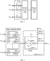
- FIG. 1 is a schematic diagram of an application manner of an existing readout circuit 100.
- one readout circuit is connected to n pixel circuits in one row, and outputs of the pixel circuits are inputs of the readout circuit.
- a working principle of the readout circuit 100 will be described below with reference to FIGS. 2 and 3.
- FIG. 2 is a schematic structural diagram of the readout circuit 100 in FIG. 1
- FIG. 3 is a timing diagram of a control manner corresponding to the readout circuit 100.
- the readout circuit 100 may mainly include the following six parts: 1 an input capacitor C 1 , where a capacitance of the input capacitor C 1 is C 1 ; 2 a feedback capacitor C 2 , where a capacitance of the feedback capacitor C 2 is C 2 ; 3 an operational amplifier (Operational Amplifier, OPA), where a gain of the OPA is -A, ideally A is ⁇ , an input voltage of the OPA is V I , and an output voltage thereof is V OUT ; 4 a sampling switch SW 1 , where a control signal of SW 1 is CLK S ; 5 one of two holding switches, SW 2 , where a control signal of SW 2 is CLK H1 ; and 6 the other of the two holding switches, SW 3 , where a control signal of SW 3 is CLK H2 .
- the foregoing three switches are all defined as: conducting when the control signal is at a high level.
- Feedback may make an input voltage V I of an ideal OPA maintain at a common mode voltage, and let the common mode voltage of the OPA be V CM and the input signal of readout circuit 100 be V IN1 during the time period t1 to t2, charges stored on the input capacitor C 1 satisfy: ( V IN 1 - V CM ) ⁇ C 1 , and charges stored on the feedback capacitor C 2 satisfy: ( V REF - V CM ) ⁇ C 2 , where V REF is a voltage of a voltage source.
- Feedback may make the input voltage V I of the ideal OPA maintain at the common mode voltage V CM , and let the input signal of readout circuit 100 be V IN2 during the time period of t3 to t4, charges stored on the input capacitor C 1 may satisfy: ( V IN 2 - V CM ) ⁇ C 1 , and charges stored on the feedback capacitor C 2 may satisfy: ( V OUT - V CM ) ⁇ C 2 .
- V IN 2 ⁇ V CM ⁇ C 1 + V OUT ⁇ V CM ⁇ C 2 V IN 1 ⁇ V CM ⁇ C 1 + V REF ⁇ V CM ⁇ C 2
- V OUT V REF + V IN 1 ⁇ V IN 2 ⁇ C 1 C 2
- sampling phase, holding phase, sampling switch, holding switch, or the like are only used to distinguish different states and different switches, and they may also be referred to as a phase 1, a phase 2, a switch 1, a switch 2, or the like.
- the readout circuit 100 may read out the effective photoelectric signal of the pixel circuit 1, and during a time period of t5 to t6, the readout circuit 100 may repeat operations of the time period of t1 to t5, and may read out an effective photoelectric signal of a pixel circuit 2. In this way, the readout circuit 100 may continuously read out effective photoelectric signals of the pixel circuit 1 to the pixel circuit n.
- the readout circuit 100 shown in FIG. 2 may only continuously read out the effective photoelectric signals of one row (or one column) of pixels.
- an image sensor there are generally m ⁇ n pixel circuits, and control of the pixel circuits is generally carried out row-by-row or column-by-column; and let m be the number of rows and n be the number of columns, one image sensor needs m (or n) of the foregoing readout circuits.
- it is a huge overhead in terms of the area and power consumption.
- an embodiment of the present application provides a readout circuit, which could reduce an area and power consumption of an image sensor.
- FIG. 4 shows a schematic diagram of a readout circuit 200 according to an embodiment of the present application.
- the readout circuit 200 may include a plurality of capacitors 210, a switch circuit 220, and an output circuit 230.
- the plurality of capacitors 210 are connected to the output circuit 230 through the switch circuit 220, the plurality of capacitors 210 are configured to store output signals of a plurality of pixel circuits, respectively, and the output circuit 230 is configured to output signals stored by the plurality of capacitors 210 through the switch circuit 220 one-by-one.
- a readout circuit includes a plurality of (for example, S) capacitors, so that output signals of S pixel circuits may be independently stored and then be output one-by-one, and the S pixel circuits may share one readout circuit; in this way, the number of readout circuits in an image sensor could be reduced to 1/S of the original value. Due to a small size of the capacitor in the readout circuit, an increased area in the readout circuit after adding the capacitor could be ignored. In addition, power consumption of the readout circuit mainly comes from an output circuit, and power consumption of the readout circuit is almost unchanged after the capacitor is added, so that an area and power consumption of the image sensor could be reduced to 1/S of the original values.
- the readout circuit of the embodiment of the present application may be applied to the field of integrated circuits.
- the readout circuit of the embodiment of the present application may be applied to an image sensor.
- the image sensor may be an optical fingerprint sensor.
- the image sensor may also be referred to as an image sensor chip or other names, and the optical fingerprint sensor may also be referred to as a fingerprint sensor, a light sensor, and a fingerprint sensor chip.
- the readout circuit of the embodiment of the present application has no special requirements on the pixel circuit and also has no special requirements on a structure of the operational amplifier, which may be, for example, a double-ended input operational amplifier, a rail-to-rail operational amplifier, a fully differential operational amplifier, or the like. Therefore, the readout circuit of the embodiment of the present application may be widely applied to the design of an existing image sensor.
- the plurality of pixel circuits may be pixel circuits in a same direction.
- the pixel circuits in the same direction herein may be pixel circuits in a same row or pixel circuits in a same column.
- the number of the plurality of capacitors 210 may be less than or equal to the number of pixel circuits.
- the number of the plurality of capacitors 210 may be less than or equal to m; and if the plurality of pixel circuits mentioned above are pixel circuits in a same row, the number of the plurality of capacitors 210 may be less than or equal to n.
- the number of the plurality of capacitors 210 is equal to the number of pixel circuits in the same direction. At this time, the number of readout circuits required in the image sensor is the smallest, and the area and power consumption of the image sensor are the smallest.
- the plurality of capacitors 210 may simultaneously sample and store the output signals of the plurality of pixel circuits.
- the plurality of capacitors 210 may simultaneously store output signals of 10 pixel circuits in the first column, and then the output circuit outputs the output signals of the 10 pixel circuits one-by-one.
- the plurality of capacitors 210 simultaneously store output signals of 10 pixel circuits in the second column, and then the output circuit outputs the output signals of the 10 pixel circuits in the second column one-by-one.
- the plurality of capacitors 210 may simultaneously store output signals of 10 pixel circuits in the fifth column, and then the output circuit outputs the output signals of the 10 pixel circuits in the fifth column one-by-one.
- the number of readout circuits may be reduced without changing the control manner of the pixel circuit, thereby reducing the area and power consumption of the image sensor.
- the plurality of capacitors 210 may not simultaneously sample and store the output signals of the plurality of pixel circuits.
- the plurality of capacitors 210 sequentially sample and store the output signals of the plurality of pixel circuits; alternatively, the plurality of capacitors 210 may be divided into a plurality of groups, the capacitors in each group sample and store the output signals of the pixel circuits at the same time, but the capacitors in different groups sample and store the output signals of the pixel circuits at different time.
- the output circuit 230 may be configured to amplify the signals stored by the plurality of capacitors 210 and output the amplified signals, and provide driving capability to the output signals.
- the embodiment of the present application does not limit an amplification factor of the amplified signal of the output circuit 230, for example, the amplification factor may be less than 1, equal to 1, or greater than 1.
- the output circuit 230 includes an operational amplifier, a feedback capacitor, a first switch, a second switch, and a third switch. Two ends of the first switch may be connected to an input end and an output end of the operational amplifier, respectively, a left plate of the feedback capacitor may be connected to the input end of the operational amplifier, a right plate of the feedback capacitor may be connected to the output end of the operational amplifier through the third switch, and two ends of the second switch may be connected to the right plate of the feedback capacitor and a voltage source, respectively.
- the first switch may also be referred to as a sampling switch, and the second switch and the third switch may also be referred to as a holding switch, respectively.
- the operational amplifier, the feedback capacitor, the first switch, the second switch, and the third switch may correspond to OPA, C 2 , SW 1 , SW 2 , and SW 3 in FIG. 2 , respectively.
- the switch circuit 220 may include only one switch, which may have a plurality of contacts.
- the number of contacts of the switch may be the same as the number of pixel circuits.
- a switch in the switch circuit 220 may be switched to be connected to the i-th capacitor, to output the signal stored by the i-th capacitor.
- the switch circuit 220 may include a plurality of switches that are in one-to-one correspondence with the plurality of capacitors 210.
- the output circuit 230 may be configured to output the signals stored by the plurality of capacitors 210 one-by-one through sequential turn-on of the plurality of switches.
- the switch corresponding to the i-th capacitor is turned on, and the remaining switches, that is, other switches in the switch circuit 220 except the switch corresponding to the i-th capacitor are turned off.
- the switch circuit 220 and the plurality of capacitors 210 may integrally form an input capacitor array.
- a schematic structural diagram of one possible readout circuit 2100 of the readout circuit 200 may be shown in FIG. 5 . It can be seen that the readout circuit 2100 may mainly include the following parts:
- FIG. 6 is a schematic diagram of one possible application manner of the readout circuit 2100.
- an image sensor includes S ⁇ n pixel circuits, and the number of a plurality of capacitors 210 is the same as the number of pixel circuits in a same column, and therefore one image sensor may only need one readout circuit.
- FIG. 7 is a timing diagram of a control manner corresponding to the readout circuit 2100 shown in FIGS. 5 and 6 .
- a working principle of the readout circuit 2100 will be described below with reference to FIG. 6 .
- all of the foregoing switches are all defined as: conducting when the control signal is at a high level.
- CLK S changes from a low level to a high level
- CLK H1 is at a high level
- CLK H2 is at a low level
- CLK P1 to CLK PS are all at high levels.
- SW S+1 starts to be turned on
- SW S+2 is turned on
- SW S+3 is turned off
- SW 1 to SW S are all turned on
- states of all the switches remain unchanged and the readout circuit 2100 operates at a sampling phase.
- Feedback may make an input voltage V I of an ideal OPA maintain at a common mode voltage.
- V CM common mode voltage of the operational amplifier
- input voltages of the readout circuit 2100 during the time period of t1 to t2 be V IN11 to V INS1
- charges stored on input capacitors C 1 to C S satisfy: ( V IN 11 - V CM ) ⁇ C 1 to ( V INS 1 - V CM ) ⁇ C S
- charges stored on feedback capacitor C F satisfy: ( V REF - V CM ) ⁇ C F , where V REF is a voltage of a voltage source.
- Feedback may make the input voltage V I of the ideal operational amplifier maintain at the common mode voltage V CM , and let an input signal of a left plate of C 1 be V IN12 during the time period of t3 to t4, charges stored on the input capacitor C 1 satisfy: ( V IN 12 - V CM ) ⁇ C 1 , and charges stored on the feedback capacitor C F satisfy: ( V OUT - V CM ) ⁇ C F .
- V IN 2 ⁇ V CM ⁇ C 1 + V OUT ⁇ V CM ⁇ C F V IN 1 ⁇ V CM ⁇ C 1 + V REF ⁇ V CM ⁇ C 2
- V OUT V REF + V IN 1 ⁇ V IN 2 ⁇ C 1 C F
- Feedback may make the input voltage V I of the ideal OPA maintain at the common mode voltage V CM .
- an input signal of a left plate of the input capacitor C 2 be V IN22 during the time period of t6 to t7, charges stored on the input capacitor C 2 satisfy ( V IN 22 - V CM ) ⁇ C 2 , and charges stored on the feedback capacitor C F satisfy: (V OUT - V CM ) ⁇ C F .
- V IN 22 ⁇ V CM ⁇ C 2 + V OUT ⁇ V CM ⁇ C F V IN 21 ⁇ V CM ⁇ C 2 + V REF ⁇ V CM ⁇ C F
- V OUT V REF + V IN 21 ⁇ V IN 22 ⁇ C 2 C F
- the readout circuit 2100 continuously reads out the effective photoelectric signals of the pixel circuit 11 to the pixel circuit S 1 (for example, the pixel circuit of the first column of the image sensor), and during a time period of t10 to t11, the readout circuit 2100 repeats the operations of the time period of t1 to t10 and may continuously read out effective photoelectric signals of pixel circuits of the second column of the image sensor, that is, a pixel circuit 12 to a pixel circuit S2. In this way, the readout circuit 2100 may continuously read out the effective photoelectric signals of the pixel circuit 11 to the pixel circuit Sn.
- sampling phase the holding phase 1 and the holding phase 2 of the readout circuit 2100 are only used to distinguish different phase states, are not intended to limit the scope of this embodiment of the present application, and they may also be referred to as a phase 1, a phase 2, a phase 3, or the like.
- the readout circuit of the embodiment of the present application may be used simultaneously with an existing image sensor technology, and there is no limitation on the image sensor technology, for example, the image sensor technology may be a multi-pixel averaging technology or the like.
- FIG. 8 is a schematic structural diagram of one possible readout circuit 2200 according to an embodiment of the present application.
- the readout circuit 2200 incorporates a pixel averaging technology, and an operational amplifier in an output circuit is a double-ended input operational amplifier.
- FIG. 9 is a schematic diagram of one possible application manner of the readout circuit 2200.
- Pixel circuits in FIG. 9 are super pixel circuits, and a structural schematic diagram of the super pixel circuits may refer to FIG. 10 . It can be seen from
- one super pixel circuit may include a plurality of sub-pixel circuits, and the one super pixel circuit may have X output signals V PO1 to V POX , where V PO1 is an output signal of a sub-pixel circuit 1 and V POX is an output signal of a sub-pixel X.
- the readout circuit 2200 may mainly include the following parts:
- Feedback may make a negative phase input voltage V I of the ideal operational amplifier be equal to a positive phase input voltage V CM .
- input voltages of the readout circuit 2200 be V IN111 to V INXS1 during the time period of t1 to t2, charges stored on input capacitors C 11 to C XS are ( V IN 111 - V CM ) ⁇ C 11 to ( V INXS1 - V CM ) ⁇ C XS , respectively, and charges stored on a feedback capacitor C F satisfy: ( V REF - V CM ) ⁇ C F .
- Feedback may make the negative phase input voltage V I of the ideal operational amplifier be equal to the positive phase input voltage V CM .
- input signals of left plates of the input capacitors C 11 to C X1 are V IN112 to V INX12 during the time period of t3 to t4
- charges stored on the input capacitors C 11 to C X1 are ( V IN 111 - V CM ) ⁇ C 11 to ( V INXS 1 - V CM ) ⁇ C XS , respectively
- charges stored on the feedback capacitor C F are ( V REF - V CM ) ⁇ C F .
- Feedback may make the negative phase input voltage V I of the ideal OPA be equal to the positive phase input voltage V CM .
- input signals of left plates of input capacitors C 12 to C X2 are V IN122 to V INX22 during the time period of t6 to t7
- charges stored on the input capacitors C 12 to C X2 are ( V IN 122 - V CM ) ⁇ C 12 to ( V INX 22 - V CM ) ⁇ C X 2 , respectively
- charges stored on the feedback capacitor C F are ( V OUT - V CM ) ⁇ C F .
- the readout circuit may continuously perform operations similar to the time period of t4 to t7 for S-2 times, and it may be obtained:
- (V sigm11 -V rstm11 ) is an effective photoelectric signal of a m-th sub-pixel circuit in the super pixel circuit 11. It can be seen from Equations (25) and (26)
- a super pixel circuit 21 may output a reset voltage ⁇ V rst121 :V rstX21 > (or a signal voltage ⁇ V sig121 :V sigX21 >), an output of the super pixel circuit 21 is used as an input of the readout circuit 2200, and the readout circuit 2200 may read out a photoelectric signal in the super pixel circuit 21:
- the readout circuit 2200 continuously reads out the effective photoelectric signals of the super pixel circuit 11 to the super pixel circuit S1 (that is, the super pixel circuit of the first column of the image sensor), and during a time period of t10 to t11, the readout circuit 2200 repeats the operations of the time period of t1 to t10 and may continuously read out effective photoelectric signals of super pixel circuits of the second column of the image sensor, that is, a super pixel circuit 12 to a super pixel circuit S2. In this way, the readout circuit 2200 may continuously read out the effective photoelectric signals of the super pixel circuit 11 to the super pixel circuit Sn.
- sampling phase, the holding phase 1 and the holding phase 2 of the readout circuit 2200 are only used to distinguish different phase states, are not intended to limit the scope of this embodiment of the present application, and they may also be referred to as a phase 1, a phase 2, a phase 3, or the like.
- a readout circuit includes a plurality of (for example, S) capacitors, so that output signals of S pixel circuits may be independently stored and then be output one-by-one, and the S pixel circuits may share one readout circuit; in this way, the number of readout circuits in an image sensor could be reduced to 1/S of the original value. Due to a small size of the capacitor in the readout circuit, an increased area in the readout circuit after adding the capacitor could be ignored. In addition, power consumption of the readout circuit mainly comes from an output circuit, and power consumption of the readout circuit is almost unchanged after the capacitor is added, so that an area and power consumption of the image sensor could be reduced to 1/S of the original values.
- An embodiment of the present application also provides an image sensor configured to convert a light signal into an electrical signal.
- the image sensor may include a readout circuit.
- the readout circuit may be the readout circuit 200 in the foregoing embodiment, and a corresponding operation of the readout circuit 200 may be realized, which is not repeatedly described herein for brevity.
- the readout circuit of the embodiment of the present application may be applied to various electronic devices, and more particularly, to an electronic device having a display screen, for example, portable or mobile computing devices such as a smart phone, a notebook computer, a tablet computer and a game device, and other electronic devices such as an electronic database, an automobile and an automated teller machine (Automated Teller Machine, ATM), which is not limited in the embodiments of the present application.
- portable or mobile computing devices such as a smart phone, a notebook computer, a tablet computer and a game device
- other electronic devices such as an electronic database, an automobile and an automated teller machine (Automated Teller Machine, ATM), which is not limited in the embodiments of the present application.
- ATM Automate Automate Machine
- An embodiment of the present application also provides an electronic device 300 as shown in FIG. 11 , and the electronic device 300 may include a readout circuit 310.
- the readout circuit 310 may be the readout circuit 200 in the foregoing embodiment, and a corresponding operation of the readout circuit 200 may be realized, which is not repeatedly described herein for brevity.
- the electronic device may further include a display screen 320.
- the display screen 320 may be a display screen with a self-emitting display unit, such as an organic light-emitting diode (Organic Light-Emitting Diode, OLED) display or a micro light-emitting diode (Micro-LED) display.
- OLED Organic Light-Emitting Diode
- Micro-LED micro light-emitting diode
- the disclosed system, apparatus and method may be implemented in other manners.
- the described apparatus embodiment is merely an example.
- the unit division is merely logical function division and may be other division in actual implementation.
- a plurality of units or components may be combined or integrated into another system, or some features may be ignored or not performed.
- the displayed or discussed mutual couplings or direct couplings or communication connections may be implemented by using some interfaces.
- the indirect couplings or communication connections between the apparatuses or units may be implemented in electrical, mechanical, or other forms.
- the units described as separate components may or may not be physically separate, and components displayed as units may or may not be physical units, may be located in one position, or may be distributed on multiple network units. Some or all of the units may be selected according to actual requirements to achieve the objectives of the solutions of the embodiments.
- the functions When the functions are implemented in the form of a software functional unit and sold or used as an independent product, the functions may be stored in a computer-readable storage medium. Based on such understanding, the nature of the technical solutions of the present application, or the part contributing to the prior art, or part of the technical solutions may be implemented in a form of software product.
- the computer software product is stored in a storage medium and includes several instructions for instructing a computer device (which may be a personal computer, a server, or a network device, and the like) to execute all of or part of the steps of the method described in the embodiments of the present application.
- the storage medium includes: various media that may store program codes, such as a U-disk, a removable hard disk, a read-only memory (ROM, Read-Only Memory), a random access memory (RAM, Random Access Memory), a magnetic disk, a compact disk, and so on.
- program codes such as a U-disk, a removable hard disk, a read-only memory (ROM, Read-Only Memory), a random access memory (RAM, Random Access Memory), a magnetic disk, a compact disk, and so on.
Landscapes
- Engineering & Computer Science (AREA)
- Multimedia (AREA)
- Signal Processing (AREA)
- Power Engineering (AREA)
- Transforming Light Signals Into Electric Signals (AREA)
Applications Claiming Priority (1)
| Application Number | Priority Date | Filing Date | Title |
|---|---|---|---|
| PCT/CN2019/092149 WO2020252754A1 (zh) | 2019-06-20 | 2019-06-20 | 读出电路、图像传感器和电子设备 |
Publications (2)
| Publication Number | Publication Date |
|---|---|
| EP3783884A1 true EP3783884A1 (de) | 2021-02-24 |
| EP3783884A4 EP3783884A4 (de) | 2021-02-24 |
Family
ID=69193253
Family Applications (1)
| Application Number | Title | Priority Date | Filing Date |
|---|---|---|---|
| EP19816183.8A Ceased EP3783884A4 (de) | 2019-06-20 | 2019-06-20 | Ausleseschaltung, bildsensor und elektronische vorrichtung |
Country Status (4)
| Country | Link |
|---|---|
| US (1) | US11303837B2 (de) |
| EP (1) | EP3783884A4 (de) |
| CN (1) | CN110710198B (de) |
| WO (1) | WO2020252754A1 (de) |
Family Cites Families (12)
| Publication number | Priority date | Publication date | Assignee | Title |
|---|---|---|---|---|
| JP4258453B2 (ja) * | 2004-08-09 | 2009-04-30 | トヨタ自動車株式会社 | 内燃機関の吸気制御装置 |
| JP4643954B2 (ja) | 2004-09-09 | 2011-03-02 | ルネサスエレクトロニクス株式会社 | 階調電圧生成回路及び階調電圧生成方法 |
| JP2007151100A (ja) * | 2005-10-31 | 2007-06-14 | Sanyo Electric Co Ltd | サンプルアンドホールド回路 |
| JP2008278453A (ja) * | 2007-04-03 | 2008-11-13 | Canon Inc | 撮像装置及び撮像システム |
| JP5288965B2 (ja) * | 2008-09-22 | 2013-09-11 | キヤノン株式会社 | 固体撮像装置及びその駆動方法 |
| JP5311954B2 (ja) * | 2008-09-30 | 2013-10-09 | キヤノン株式会社 | 固体撮像装置の駆動方法 |
| CN102497517B (zh) * | 2011-11-25 | 2013-09-11 | 吉林大学 | 低工作电压宽动态范围图像传感器 |
| JP6012314B2 (ja) * | 2012-07-12 | 2016-10-25 | キヤノン株式会社 | 読出回路及び固体撮像装置 |
| JP6893325B2 (ja) * | 2016-03-16 | 2021-06-23 | パナソニックIpマネジメント株式会社 | 反転増幅器、積分器、サンプルホールド回路、ad変換器、イメージセンサ、および撮像装置 |
| CN110771157B (zh) * | 2017-03-31 | 2022-02-08 | 普里露尼库斯新加坡私人有限公司 | 固态摄像装置、固态摄像装置的驱动方法、以及电子机器 |
| CN107613179B (zh) * | 2017-10-23 | 2019-11-12 | 德淮半导体有限公司 | 一种图像传感器及其输出电路 |
| CN109787563B (zh) * | 2019-01-16 | 2021-08-24 | 电子科技大学 | 一种基于运放失调补偿的相关双采样电路 |
-
2019
- 2019-06-20 EP EP19816183.8A patent/EP3783884A4/de not_active Ceased
- 2019-06-20 WO PCT/CN2019/092149 patent/WO2020252754A1/zh not_active Ceased
- 2019-06-20 CN CN201980002482.5A patent/CN110710198B/zh active Active
- 2019-12-14 US US16/714,714 patent/US11303837B2/en active Active
Also Published As
| Publication number | Publication date |
|---|---|
| WO2020252754A1 (zh) | 2020-12-24 |
| CN110710198B (zh) | 2021-08-13 |
| US20200404206A1 (en) | 2020-12-24 |
| US11303837B2 (en) | 2022-04-12 |
| CN110710198A (zh) | 2020-01-17 |
| EP3783884A4 (de) | 2021-02-24 |
Similar Documents
| Publication | Publication Date | Title |
|---|---|---|
| CN106326859B (zh) | 指纹识别驱动电路、阵列基板、显示装置及指纹识别方法 | |
| CN104795018B (zh) | 移位寄存器、驱动方法、栅极驱动电路及显示装置 | |
| US11784659B2 (en) | Circuit system for weight modulation and image recognition of memristor array | |
| US20200412930A1 (en) | Event detecting device including an event signal generator and an output signal generator | |
| CN110008860B (zh) | 指纹识别架构及触控面板 | |
| WO2020107435A1 (zh) | 扫描电路、驱动电路、触控显示面板、接收切换电路及驱动方法 | |
| US20180211080A1 (en) | Fingerprint Identification Circuit, Touch Apparatus and Fingerprint Identification Method | |
| CN112835474A (zh) | 触控面板及其驱动方法和显示装置 | |
| CN107066960B (zh) | 一种用于指纹传感器的信号处理电路 | |
| US10528200B2 (en) | Coordinate measurement device and method for hover sensing | |
| CN101349821A (zh) | 用以得知光线强度的读取电路及电子系统 | |
| US10324573B2 (en) | Sensing devices for sensing electrical characteristics | |
| US11984080B2 (en) | Pixel compensation circuit and driving method therefor, and display apparatus | |
| CN111741240B (zh) | 图像传感器、指纹检测装置和电子设备 | |
| US11978279B2 (en) | Fingerprint identification circuit, display panel and control method thereof | |
| US20190012969A1 (en) | Source drive circuit, and liquid crystal display panel and method of driving the same | |
| EP3985555A1 (de) | Bildsensor, fingerabdruckerkennungseinrichtung und elektronische vorrichtung | |
| EP3783884A1 (de) | Ausleseschaltung, bildsensor und elektronische vorrichtung | |
| CN210007779U (zh) | 读出电路、图像传感器和电子设备 | |
| US12086354B2 (en) | Analog front end and touch display device | |
| CN117519506A (zh) | 触控检测电路及触控显示装置 | |
| CN114637423B (zh) | 显示面板及其驱动方法、显示装置 | |
| JP3379873B2 (ja) | マトリックス型タッチパネル入力装置 | |
| EP3493096B1 (de) | Fingerabdrucksensor und endgerätevorrichtung | |
| CN109726704B (zh) | 屏幕信号采集装置及方法 |
Legal Events
| Date | Code | Title | Description |
|---|---|---|---|
| STAA | Information on the status of an ep patent application or granted ep patent |
Free format text: STATUS: UNKNOWN |
|
| STAA | Information on the status of an ep patent application or granted ep patent |
Free format text: STATUS: THE INTERNATIONAL PUBLICATION HAS BEEN MADE |
|
| PUAI | Public reference made under article 153(3) epc to a published international application that has entered the european phase |
Free format text: ORIGINAL CODE: 0009012 |
|
| STAA | Information on the status of an ep patent application or granted ep patent |
Free format text: STATUS: REQUEST FOR EXAMINATION WAS MADE |
|
| 17P | Request for examination filed |
Effective date: 20191216 |
|
| A4 | Supplementary search report drawn up and despatched |
Effective date: 20200929 |
|
| AK | Designated contracting states |
Kind code of ref document: A1 Designated state(s): AL AT BE BG CH CY CZ DE DK EE ES FI FR GB GR HR HU IE IS IT LI LT LU LV MC MK MT NL NO PL PT RO RS SE SI SK SM TR |
|
| AX | Request for extension of the european patent |
Extension state: BA ME |
|
| STAA | Information on the status of an ep patent application or granted ep patent |
Free format text: STATUS: EXAMINATION IS IN PROGRESS |
|
| 17Q | First examination report despatched |
Effective date: 20210708 |
|
| 17Q | First examination report despatched |
Effective date: 20210813 |
|
| DAV | Request for validation of the european patent (deleted) | ||
| DAX | Request for extension of the european patent (deleted) | ||
| REG | Reference to a national code |
Ref country code: DE Ref legal event code: R003 |
|
| STAA | Information on the status of an ep patent application or granted ep patent |
Free format text: STATUS: THE APPLICATION HAS BEEN REFUSED |
|
| 18R | Application refused |
Effective date: 20221003 |