EP3780104B1 - Kameraanordnung, montageverfahren dafür und endgerät - Google Patents
Kameraanordnung, montageverfahren dafür und endgerät Download PDFInfo
- Publication number
- EP3780104B1 EP3780104B1 EP19864283.7A EP19864283A EP3780104B1 EP 3780104 B1 EP3780104 B1 EP 3780104B1 EP 19864283 A EP19864283 A EP 19864283A EP 3780104 B1 EP3780104 B1 EP 3780104B1
- Authority
- EP
- European Patent Office
- Prior art keywords
- rdl
- infrared filter
- image sensor
- hole
- camera assembly
- Prior art date
- Legal status (The legal status is an assumption and is not a legal conclusion. Google has not performed a legal analysis and makes no representation as to the accuracy of the status listed.)
- Active
Links
Images
Classifications
-
- H—ELECTRICITY
- H10—SEMICONDUCTOR DEVICES; ELECTRIC SOLID-STATE DEVICES NOT OTHERWISE PROVIDED FOR
- H10F—INORGANIC SEMICONDUCTOR DEVICES SENSITIVE TO INFRARED RADIATION, LIGHT, ELECTROMAGNETIC RADIATION OF SHORTER WAVELENGTH OR CORPUSCULAR RADIATION
- H10F39/00—Integrated devices, or assemblies of multiple devices, comprising at least one element covered by group H10F30/00, e.g. radiation detectors comprising photodiode arrays
- H10F39/011—Manufacture or treatment of image sensors covered by group H10F39/12
- H10F39/018—Manufacture or treatment of image sensors covered by group H10F39/12 of hybrid image sensors
-
- H—ELECTRICITY
- H10—SEMICONDUCTOR DEVICES; ELECTRIC SOLID-STATE DEVICES NOT OTHERWISE PROVIDED FOR
- H10F—INORGANIC SEMICONDUCTOR DEVICES SENSITIVE TO INFRARED RADIATION, LIGHT, ELECTROMAGNETIC RADIATION OF SHORTER WAVELENGTH OR CORPUSCULAR RADIATION
- H10F39/00—Integrated devices, or assemblies of multiple devices, comprising at least one element covered by group H10F30/00, e.g. radiation detectors comprising photodiode arrays
- H10F39/80—Constructional details of image sensors
- H10F39/804—Containers or encapsulations
-
- H—ELECTRICITY
- H04—ELECTRIC COMMUNICATION TECHNIQUE
- H04N—PICTORIAL COMMUNICATION, e.g. TELEVISION
- H04N23/00—Cameras or camera modules comprising electronic image sensors; Control thereof
- H04N23/50—Constructional details
- H04N23/55—Optical parts specially adapted for electronic image sensors; Mounting thereof
-
- G—PHYSICS
- G02—OPTICS
- G02B—OPTICAL ELEMENTS, SYSTEMS OR APPARATUS
- G02B5/00—Optical elements other than lenses
- G02B5/20—Filters
- G02B5/208—Filters for use with infrared or ultraviolet radiation, e.g. for separating visible light from infrared and/or ultraviolet radiation
-
- G—PHYSICS
- G02—OPTICS
- G02B—OPTICAL ELEMENTS, SYSTEMS OR APPARATUS
- G02B7/00—Mountings, adjusting means, or light-tight connections, for optical elements
- G02B7/006—Filter holders
-
- G—PHYSICS
- G03—PHOTOGRAPHY; CINEMATOGRAPHY; ANALOGOUS TECHNIQUES USING WAVES OTHER THAN OPTICAL WAVES; ELECTROGRAPHY; HOLOGRAPHY
- G03B—APPARATUS OR ARRANGEMENTS FOR TAKING PHOTOGRAPHS OR FOR PROJECTING OR VIEWING THEM; APPARATUS OR ARRANGEMENTS EMPLOYING ANALOGOUS TECHNIQUES USING WAVES OTHER THAN OPTICAL WAVES; ACCESSORIES THEREFOR
- G03B11/00—Filters or other obturators specially adapted for photographic purposes
-
- H—ELECTRICITY
- H04—ELECTRIC COMMUNICATION TECHNIQUE
- H04N—PICTORIAL COMMUNICATION, e.g. TELEVISION
- H04N23/00—Cameras or camera modules comprising electronic image sensors; Control thereof
- H04N23/50—Constructional details
-
- H—ELECTRICITY
- H04—ELECTRIC COMMUNICATION TECHNIQUE
- H04N—PICTORIAL COMMUNICATION, e.g. TELEVISION
- H04N23/00—Cameras or camera modules comprising electronic image sensors; Control thereof
- H04N23/50—Constructional details
- H04N23/54—Mounting of pick-up tubes, electronic image sensors, deviation or focusing coils
-
- H—ELECTRICITY
- H04—ELECTRIC COMMUNICATION TECHNIQUE
- H04N—PICTORIAL COMMUNICATION, e.g. TELEVISION
- H04N23/00—Cameras or camera modules comprising electronic image sensors; Control thereof
- H04N23/57—Mechanical or electrical details of cameras or camera modules specially adapted for being embedded in other devices
-
- H—ELECTRICITY
- H10—SEMICONDUCTOR DEVICES; ELECTRIC SOLID-STATE DEVICES NOT OTHERWISE PROVIDED FOR
- H10F—INORGANIC SEMICONDUCTOR DEVICES SENSITIVE TO INFRARED RADIATION, LIGHT, ELECTROMAGNETIC RADIATION OF SHORTER WAVELENGTH OR CORPUSCULAR RADIATION
- H10F39/00—Integrated devices, or assemblies of multiple devices, comprising at least one element covered by group H10F30/00, e.g. radiation detectors comprising photodiode arrays
- H10F39/80—Constructional details of image sensors
- H10F39/809—Constructional details of image sensors of hybrid image sensors
Definitions
- This application relates to the field of semiconductor technologies, and more specifically, to a camera assembly, an assembly method, and a terminal.
- the camera module As the design of current mobile phones tends to be miniaturized and ultra-thin, the camera module, as an important module component of the mobile phone, also faces the challenges of miniaturization and ultra-thinness. In particular, the current high screen-to-body ratio and the full screen design have increased the need for a reduction in the outer dimensions of the camera module.
- the document US 2008/083980 A1 is a relevant prior art.
- An architecture of a conventional camera module includes a printed circuit board (printed circuit board, PCB), a soldering process, a gold wire bonding process, and the like.
- PCB printed circuit board
- soldering process soldering process
- gold wire bonding process gold wire bonding process
- This application provides a camera assembly, an assembly method, and a terminal, so as to implement an electrical connection between electronic components through metal wiring at a redistribution layer (redistribution layer, RDL). Because the RDL is thinner than the PCB board in a conventional camera module, the electrical connection between electronic components is implemented by replacing the PCB with the RDL, so that the overall height of the camera module can be reduced.
- RDL redistribution layer
- a method for assembling a camera assembly including the following steps:
- the electrical connection between the electronic components can be implemented through the metal wiring at the RDL. Because the RDL is thinner than the PCB board in a conventional camera module, when the electrical connection between the electronic components is implemented by replacing the PCB with the RDL, the overall height of the camera module can be reduced.
- the method further includes: fixing an infrared filter to a second surface of the RDL.
- the second surface of the RDL faces away from the first surface of the RDL.
- the infrared filter is opposite the through-hole, and light passing through the infrared filter is incident on the image sensor through the through-hole.
- the infrared filter can be fixed to the second surface of the RDL, so that the overall height of the camera module can be reduced.
- the infrared filter is fixed in the through-hole.
- the infrared filter can be fixed in the through-hole at the RDL, so that the impact of the infrared filter on the height of the camera module can be further reduced, and the overall height of the camera module can be reduced.
- a motor is fixed to the second surface of the RDL.
- any possible implementation of the first aspect further including: fixing a holder to the second surface of the RDL.
- the holder is configured to support the infrared filter.
- the infrared filter is opposite the through-hole, and light passing through the infrared filter is incident on the image sensor through the through-hole.
- the infrared filter can be fixed to the second surface of the RDL using the holder, so that the infrared filter can be closer to the lens, and the infrared light can be better blocked from entering the image sensor.
- a motor is fixed to the holder, and the motor and the RDL are respectively located on both sides of the holder.
- the surface mount electronic component and the image sensor are placed on a tray fixture.
- the surface mount electronic component and the image sensor are wrapped by an encapsulating material.
- the surface mount electronic component and the image sensor in the target encapsulated module can be positioned using the encapsulating material, so that the electrical connection between the electronic components can be better implemented.
- the encapsulating material is an epoxy resin material.
- a camera assembly including a target encapsulated module and a redistribution layer RDL.
- RDL redistribution layer
- a surface mount electronic component and an image sensor are encapsulated on the target encapsulated module.
- the target encapsulated module includes an active surface, and a solder end of the surface mount electronic component and the solder end of the image sensor are exposed on the active surface.
- the redistribution layer RDL is provided with a through-hole.
- the through-hole is opposite a photosensitive area of the image sensor.
- the RDL includes a dielectric layer and metal wiring disposed at the dielectric layer. The metal wiring is at least partially exposed on a first surface of the RDL.
- the metal wiring exposed on the first surface of the RDL is connected to a solder end on the active surface of the target encapsulated module.
- the electrical connection between the electronic components can be implemented through the metal wiring at the RDL. Because the RDL is thinner than the PCB board in a conventional camera module, when the electrical connection between the electronic components is implemented by replacing the PCB with the RDL, the overall height of the camera module can be reduced.
- the camera assembly further includes an infrared filter, where the infrared filter is fixed to a second surface of the RDL.
- the second surface of the RDL faces away from the first surface of the RDL.
- the infrared filter is opposite the through-hole, and light passing through the infrared filter is incident on the image sensor through the through-hole.
- the infrared filter can be fixed to the second surface of the RDL, so that the overall height of the camera module can be reduced.
- the camera assembly further includes an infrared filter, where the infrared filter is fixed in the through-hole.
- the infrared filter can be fixed in the through-hole at the RDL, so that the impact of the infrared filter on the height of the camera module can be further reduced, and the overall height of the camera module can be reduced.
- the camera assembly further includes a motor, where the motor is fixed to the second surface of the RDL.
- the camera assembly further includes a holder and an infrared filter.
- the holder is configured to support the infrared filter.
- the holder is fixed to the second surface of the RDL.
- the infrared filter is opposite the through-hole, and light passing through the infrared filter is incident on the image sensor through the through-hole.
- the infrared filter can be fixed to the second surface of the RDL using the holder, so that the infrared filter can be closer to the lens, and the infrared light can be better blocked from entering the image sensor.
- the camera assembly further includes a motor, where the motor is fixed to the holder, and the motor and the RDL are respectively located on both sides of the holder.
- the target encapsulated module further includes an encapsulating material.
- the encapsulating material surrounds a surface mount electronic component in the target encapsulated module and an image sensor.
- the surface mount electronic component and the image sensor in the target encapsulated module can be positioned using the encapsulating material, so that the electrical connection between the electronic components can be better implemented.
- the encapsulating material is an epoxy resin material.
- a terminal including a camera assembly according to the second aspect or any possible implementation of the second aspect and a processor configured to control the camera assembly.
- the type of a terminal device mentioned in the embodiments of this application is not specifically limited, and the terminal device may include, but is not limited to, a mobile station (mobile station, MS), a mobile telephone (mobile telephone), user equipment (UE), a handset (handset), portable equipment (portable equipment), a cellular telephone, a cordless telephone, a session initiation protocol (session initiation protocol, SIP) telephone, a wireless local loop (wireless local loop, WLL) station, a personal digital assistant (personal digital assistant, PDA), a radio frequency identification (radio frequency identification, RFID) terminal device for logistics, a handheld device having a wireless communication function, a computing device, another device connected to a wireless modem, an in-vehicle device, a wearable device, or a terminal device in an Internet of Things or an Internet of vehicles.
- a mobile station mobile station
- UE user equipment
- UE handset
- portable equipment portable equipment
- a cellular telephone a cordless telephone
- session initiation protocol session initiation protocol
- WLL
- the terminal device may alternatively be a wearable device.
- a wearable device may also be referred to as a wearable smart device, and is a general term for daily wearable devices that are smartly designed and developed by using wearable technologies, such as glasses, gloves, watches, apparels, and shoes.
- a wearable device is a portable device that can be worn directly on the body or integrated into the clothing or accessories of a user.
- the wearable device is not merely a hardware device, it can implement a powerful function based on software support, and data interaction, and cloud interaction.
- Generalized wearable smart devices include large-sized smart devices that can implement some functions without relying on a smartphone, such as smartwatches or smart glasses, and also include smart devices that focus on a particular application function and need to work with another device such as a smartphone, such as smart bands and smart jewelry that are used for sign monitoring.
- An embodiment of this application provides a camera assembly, so as to implement electrical connection between electronic components through metal wiring at a redistribution layer (redistribution layer, RDL). Because the RDL is thinner than the PCB board in a conventional camera module, the electrical connection between the electronic components is implemented by replacing the PCB with the RDL, so that the overall height of the camera module can be reduced.
- RDL redistribution layer
- a method for assembling a camera assembly according to an embodiment of this application is described in detail below with reference to FIG. 1 .
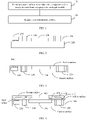
- FIG. 1 is a schematic block diagram of a method for assembling a camera assembly according to an embodiment of this application.
- the assembly method shown in FIG. 1 may include steps 110-120. Steps 110-120 are described in detail below.
- Step 110 Encapsulate a surface mount electronic component and an image sensor to form a target encapsulated module.
- the surface mount electronic component is not specifically limited in this embodiment of this application.
- the surface mount electronic component may be a surface mount device (surface mount device, SMD).
- the SMD may be a surface mount resistive component, a surface mount capacitive device, a small-outline transistor (small-outline transistor, SOT), a small outline integrated circuit (small outline integrated circuit, SOIC) component, or an array chip (for example, a ball grid array (ball grid array, BGA) component, or a micro lead frame (micro lead frame, MLF) component).
- the surface mount device SMD may include, but is not limited to, at least one of the following models: 0201, 0402, 0603, 0805, 1206, 1210, or 2010.
- the SOT transistor may include, but is not limited to, at least one of the following models: SOT23, SOT143, or SOT89.
- the SOIC component may include, but is not limited to, at least one of the following models: SOIC08, SOIC14, SOIC16, SOIC18, SOIC20, SOIC24, SOIC28, or SOIC32.
- the BGA component may be a plastic ball grid array (plastic ball grid array, PBGA) component, an erasable programmable read only memory (erasable programmable read only memory, EPROM) component, or a ceramic plastic ball grid array (ceramic plastic ball grid array, CBGA) component.
- PBGA plastic ball grid array
- EPROM erasable programmable read only memory
- CBGA ceramic plastic ball grid array
- an encapsulating process may be performed to position the surface mount electronic component and the image sensor.
- the molten epoxy resin can be injected into a mold using a high temperature injection molding technology, to wrap various components (for example, the image sensor and at least one surface mount electronic component) in the mold, so that an encapsulated module is formed and each component in the mold is positioned. A solder end of the surface mount electronic component and the solder end of the image sensor in the encapsulated module are exposed on the active surface of the encapsulated module.
- Step 120 Prepare an RDL.
- the RDL may be prepared on a target encapsulated module formed through encapsulating in step 110.
- the RDL may include a dielectric layer and a plurality of metal wirings disposed at the dielectric layer, and at least a part of each metal wiring is disposed on a first surface of the dielectric layer or a second surface opposite the first surface. It should be understood that, for each metal wiring, the remaining part is located at the dielectric layer, except for the part that is located on the first surface or the second surface of the dielectric layer.
- the dielectric layer (which may also be referred to as a substrate) may be used to maintain insulation between portions of each metal wiring located at the dielectric layer and other electronic components located outside the dielectric layer.
- the plurality of metal wirings include two or more metal wirings. It should be noted that the first surface of the dielectric layer is opposite the active surface of the target encapsulated module, or the first surface of the dielectric layer faces the active surface of the target encapsulated module. Accordingly, the second surface of the dielectric layer faces away from the first surface of the dielectric layer.
- the metal wiring exposed on the first surface of the dielectric layer is connected to the solder ends that are of at least one surface mount electronic component and the image sensor and that are exposed on the active surface of the encapsulated module.
- first surface of the dielectric layer is also the first surface of the RDL
- second surface of the dielectric layer is also the second surface of the RDL. That is, being exposed on the first surface of the dielectric layer can be understood as being exposed on the first surface of the RDL, and being exposed on the second surface of the dielectric layer can be understood as being exposed on the second surface of the RDL.
- descriptions of the same or similar cases will be omitted below.
- the RDL in this embodiment of this application is provided with a through-hole.
- the through-hole is opposite a photosensitive area of the image sensor in the encapsulated module, so that the photosensitive area of the image sensor is exposed, and a light signal can be transmitted to the photosensitive area of the image sensor through the through-hole on the RDL.
- An embodiment of this application provides a camera assembly, so as to implement electrical connection between electronic components through metal wiring at a redistribution layer RDL. Because the RDL is thinner than the PCB board in a conventional camera module, the electrical connection between the electronic components is implemented by replacing the PCB with the RDL, so that the overall height of the camera module can be reduced.
- the camera module may further include an infrared filter.
- An infrared filter can also be understood as an optical structure with infrared light filtering. The infrared filter can block the passage of filtered visible light while allowing the passage of infrared light, so that the infrared light can be separated in a light environment in which visible light and infrared light are mixed.
- the infrared filter may be fixed to the second surface of the RDL.
- the infrared filter is opposite the through-hole at the RDL, and the infrared filter and the image sensor in encapsulated module are respectively located on both sides of the RDL.
- the infrared filter may also be embedded in the through-hole at the RDL.
- the camera module may also include a holder, where the holder may be configured to support the infrared filter. The holder is fixed to the second surface of the RDL, and the infrared filter is opposite the through-hole at the RDL.
- FIG. 2 and FIG. 3 Specific implementations of forming a target encapsulated module through an injection molding process in this embodiment of this application are described in more detail below with reference to FIG. 2 and FIG. 3 .
- FIG. 2 and FIG. 3 are merely intended to help those skilled in the art understand the embodiments of this application, and are not intended to limit the embodiments of this application to the specific values or specific scenarios illustrated.
- a person skilled in the art can apparently make various equivalent modifications or changes according to the examples shown in FIG. 2 to FIG. 3 , and such modifications or changes also fall within the scope of the embodiments of this application.
- FIG. 2 is a schematic structural diagram of an assembled electronic component according to an embodiment of this application.
- FIG. 2 may include a tray fixture 210, an image sensor 220, and an SMD device 230.
- This embodiment of this application does not specifically limit the type of the image sensor 220.
- a charge-coupled device (charge-coupled device, CCD) image sensor may be used
- a complementary metal oxide semiconductor (complementary metal oxide semiconductor, CMOS) image sensor may be used
- a photoelectric image sensor may be used.
- the tray fixture 210 may be a load-bearing fixture that covers the adhesive material (for example, glue) on one side.
- the SMD device 230 and the image sensor 220 may be attached to the tray tool 210 (by using glue) based on the design. After the SMD device 230 and the image sensor 220 are attached to the tray fixture 210, the SMD device 230 and the image sensor 220 may be encapsulated through an encapsulating process.
- the encapsulating technology can be injecting molten epoxy into the surroundings of the SMD device 230 and the image sensor 220 using a high temperature injection molding technology, so as to wrap the SMD device 230 and the image sensor 220. Then the encapsulated module may be removed from the tray fixture 210.
- the encapsulating time may be 20 to 40 seconds
- the curing time may be 2 to 3 minutes
- the curing temperature may be 180°C.
- FIG. 3 is a schematic structural diagram of a target encapsulated module 300 according to an embodiment of this application.
- target encapsulated module 300 may correspond to the encapsulated module described in FIG. 2 .
- the target encapsulated module 300 may include an active surface and a passive surface (where the active surface of the target encapsulated module 300 is opposite the passive surface). Soldering pads (also referred to as pins) of the SMD device 230 and the image sensor 220 are exposed on the active surface. An RDL may be fabricated on the soldering pads to implement electrical connection between the SMD device 230 and the image sensor 220.
- the soldering pads of the SMD device 230 and the image sensor 220 may be exposed on the surface of the active surface of the target encapsulated module 300.
- the soldering pads that are of the SMD device 230 and the image sensor 220 and that are exposed on the surface of the active surface of the target encapsulated module 300 may be connected to metal wiring in the prepared RDL, so as to implement electrical connection between the SMD device 230 and the image sensor 220.
- FIG. 4 is a schematic structural diagram of an RDL and the target encapsulated module 300 according to an embodiment of this application.
- the RDL 410 shown in FIG. 4 may be located on one side of the target encapsulated module 300 (for example, the active surface of the target encapsulated module 300).
- the procedure of preparing the RDL 410 on the active surface of the target encapsulated module 300 is described in detail below.
- the dielectric layer 420 is located on the active surface of the target encapsulated module 300, or the dielectric layer 420 is located on the active surface side of the target encapsulated module 300.
- a metal wiring 430 is provided at the dielectric layer 420.
- An exposed part of the metal wiring 430 on the first surface of the dielectric layer 420 may be interconnected with the soldering pads that are of the SMD device 230 and the image sensor 220 and that are exposed on the active surface of the target encapsulated module 300, so as to implement electrical connection between the SMD device 230 and the image sensor 220.
- the exposed part of the metal wiring 430 on the first surface of the dielectric layer 420 may be understood as that the metal wiring 430 is partially exposed on the first surface of the dielectric layer 420.
- the exposed part of the dielectric layer 420 on the first surface of the dielectric layer 420 may be connected to the soldering pads that are of the SMD device 230 and the image sensor 220 and that are exposed on the surface of the active surface of the target encapsulated module 300, so as to implement electrical connection between electronic components (for example, the image sensor 220 and the plurality of SMD devices 230 in FIG. 4 ).
- the RDL 410 is provided with a through-hole 440.
- the through-hole 440 is opposite the photosensitive area of the image sensor 220, so that the photosensitive area of the image sensor 220 is exposed, and a light signal can be incident on the photosensitive area of the image sensor 220 through the through-hole 440 at the RDL 410.
- the metal wiring 430 may be a metal material, for example, copper or aluminum.
- the dielectric layer 420 may be an insulating material, for example, polyimide (polyimide, PI), solder resist film (solder resist film, SRF), or benzocyclobutene (benzocyclobutene, BCB).
- each dielectric layer 420 may be designed to be 20 um; the line width of the metal wiring 430 may be designed to be 5 um; and the spacing between the at least one metal wiring 430 may be designed to be 5 um.
- the RDL 410 may be prepared through processes such as sputtering deposition to a surface, anticorrosion coating, exposure molding with a line lithography system, development, and electrochemical deposition for implementing a copper line layer.
- the camera module may further include an infrared filter and a motor.
- the infrared filter may be fixed to the second surface of the RDL.
- the infrared filter is opposite the through-hole at the RDL, and the infrared filter and the image sensor in encapsulated module are respectively located on both sides of the RDL.
- the motor may be fixed to the second surface of the RDL.
- FIG. 5 A possible camera assembly in an embodiment of this application is described in more detail below with reference to FIG. 5 .
- FIG. 5 is merely intended to help those skilled in the art understand this embodiment of this application, and is not intended to limit this embodiment of this application to the specific value or specific scenario illustrated.
- a person skilled in the art can apparently make various equivalent modifications or changes according to the examples shown in FIG. 5 , and such modifications or changes also fall within the scope of the embodiments of this application.
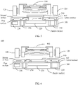
- FIG. 5 is a schematic structural diagram of a camera assembly 500 according to an embodiment of this application.
- the camera assembly 500 may include a target encapsulated module 300, an RDL 410, an infrared filter 510, a motor 520, and a lens 530.
- the target encapsulated module 300 is an image sensor 220 and a plurality of SMD devices 230.
- the type of the motor 520 is not specifically limited in this embodiment of this application.
- the motor 520 may be, for example, a voice coil motor (voice coil motor, VCM) or an optical zoom motor.
- the infrared filter 510 is located on the second surface of the RDL 410.
- the motor 520 is also located on the second surface of the RDL 410, and the infrared filter 510 is isolated from the motor 520.
- the infrared filter 510 is opposite the through-hole 440 at the RDL 410, and the infrared filter 510 and the image sensor 220 are respectively located on both sides of the RDL 410.
- the infrared filter 510 may be fixed to the second surface of the RDL 410. Further, the motor 520 may be fixed to the second surface of the RDL 410. Still further, the lens 530 may be fixed to the side of the infrared filter 510 facing away from the RDL410 by the motor 520, so that light passing through the infrared filter 510 is incident on the photosensitive area of the image sensor 220 through the through-hole 440, and the assembly of the camera module 500 is completed.
- the fixing may be implemented using an adhesive material, and the adhesive material may be, for example, glue.
- the infrared filter can be fixed to the second surface of the RDL, so that the overall height of the camera module can be reduced.
- the camera module further includes an infrared filter and a motor.
- the infrared filter is fixed in the through-hole. It should be understood that the infrared filter 510 in the camera assembly 500 shown in FIG. 5 may be embedded in the through-hole 440 at the RDL 410.
- the motor is fixed to the second surface of the RDL.
- the outer side wall of the infrared filter 510 is in contact with the inner side wall of the through-hole 440.
- the infrared filter 510 is specifically clamped in the through-hole 440, so that the infrared filter 510 is fixed in the through-hole 440.
- the clamping of the infrared filter 510 in the through-hole 440 means that the outer side wall of the infrared filter 510 and the inner side wall of the through-hole 440 are pressed against each other, so that the frictional force between them can carry the infrared filter 510, thereby fixing the infrared filter 510 in the through-hole 440.
- FIG. 6 A possible camera assembly in an embodiment of this application is described in more detail below with reference to FIG. 6 . It should be noted that the example in FIG. 6 is merely intended to help those skilled in the art understand this embodiment of this application, and is not intended to limit this embodiment of this application to the specific value or specific scenario illustrated. A person skilled in the art can apparently make various equivalent modifications or changes according to the examples shown in FIG. 6 , and such modifications or changes also fall within the scope of the embodiments of this application.
- FIG. 6 is a schematic structural diagram of a possible camera assembly 600 according to an embodiment of this application.
- the camera assembly 600 may include a target encapsulated module 300, an RDL 410, an infrared filter 510, a motor 520, and a lens 530.
- the target encapsulated module 300 is an image sensor 220 and a plurality of SMD devices 230.
- the infrared filter 510 is located in the through-hole 440 of the RDL 410.
- One side of the infrared filter 510 is opposite the image sensor 220.
- the motor 520 is located on the second surface of the RDL 410.
- the infrared filter 510 may be fixed in the through-hole 440 at the RDL 410. Further, the motor 520 may be fixed to the second surface of the RDL 410. Still further, the lens 530 is fixed to the side of the infrared filter 510 facing away from the image sensor 220 by the motor 520, so that light passing through the infrared filter 510 is incident on the photosensitive area of the image sensor 220, and the assembly of the camera module 600 is completed.
- the fixing may be implemented using an adhesive material, and the adhesive material may be, for example, glue.
- the infrared filter can be embedded (or clamped) in the through-hole at the RDL, thereby reducing the height of the camera module in the infrared filter.
- the camera assembly further includes a holder, an infrared filter, and a motor.
- the holder may be configured to support the infrared filter 510 in the camera assembly 500 shown in FIG. 5 .
- the holder is fixed to the second surface of the RDL.
- the infrared filter 510 is opposite the through-hole 440 at the RDL 410, and light passing through the infrared filter 510 is incident on the image sensor 220 through the through-hole 440.
- the motor is fixed to the holder, and the motor and the RDL are respectively located on both sides of the holder.
- FIG. 7 A possible camera assembly in an embodiment of this application is described in more detail below with reference to FIG. 7 . It should be noted that the example in FIG. 7 is merely intended to help those skilled in the art understand this embodiment of this application, and is not intended to limit this embodiment of this application to the specific value or specific scenario illustrated. A person skilled in the art can apparently make various equivalent modifications or changes according to the examples shown in FIG. 7 , and such modifications or changes also fall within the scope of the embodiments of this application.
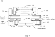
- FIG. 7 is a schematic structural diagram of a possible camera assembly 700 according to an embodiment of this application.
- the camera assembly 700 may include a target encapsulated module 300, an RDL 410, an infrared filter 510, a motor 520, a lens 530, and a holder 710.
- the target encapsulated module 300 is an image sensor 220 and a plurality of SMD devices 230.
- the holder 710 is located on the second surface of the RDL 410.
- the holder 710 may be configured to support the infrared filter 510.
- the infrared filter 510 is opposite the through-hole 440 at the RDL 410, and the infrared filter 510 and the image sensor 220 are respectively located on both sides of the RDL410.
- the motor 520 is located on the holder 710, and the motor 520 and the RDL 410 are respectively located on both sides of the holder 710.
- the holder 710 may be fixed to the second surface of the RDL 410.
- the infrared filter 510 may be fixed to the holder 710.
- the motor 520 may be fixed to the holder 710, and the motor 520 and the RDL 410 are respectively located on both sides of the holder 710.
- the lens 530 may be fixed to the side of the infrared filter 510 facing away from the RDL410 by the motor 520, so that light passing through the infrared filter 510 is incident on the photosensitive area of the image sensor 220 through the through-hole 440, and the assembly of the camera module 700 is completed.
- the fixing may be implemented using an adhesive material, and the adhesive material may be, for example, glue.
- the infrared filter can be fixed to the second surface of the RDL using the holder, so that the infrared filter can be closer to the lens, and the infrared light can be better blocked from entering the image sensor.
Landscapes
- Engineering & Computer Science (AREA)
- Multimedia (AREA)
- Signal Processing (AREA)
- Physics & Mathematics (AREA)
- General Physics & Mathematics (AREA)
- Optics & Photonics (AREA)
- Health & Medical Sciences (AREA)
- Toxicology (AREA)
- Studio Devices (AREA)
Claims (15)
- Verfahren zum Montieren einer Kameraanordnung (500, 600, 700), wobei das Verfahren Folgendes umfasst:Kapseln einer oberflächenmontierten elektronischen Komponente (230) und eines Bildsensors (220), um ein gekapseltes Zielmodul zu bilden, wo das gekapselte Zielmodul eine aktive Fläche beinhaltet und ein Lotende der oberflächenmontierten elektronischen Komponente und ein Lotende des Bildsensors auf der aktiven Fläche freiliegen;Vorbereiten einer Umverteilungsschicht RDL (410) und Bohren der RDL, um ein Durchgangsloch (440) zu bilden, wo das Durchgangsloch einem photosensitiven Bereich des Bildsensors gegenüberliegt, die RDL eine Dielektrikumschicht (420) und eine Metallverdrahtung (430), die an der Dielektrikumschicht angeordnet ist, beinhaltet und die Metallverdrahtung mindestens teilweise auf einer ersten Fläche der RDL freiliegt; undVerbinden der Metallverdrahtung, die auf der ersten Fläche der RDL freiliegt, mit dem Lotende der oberflächenmontierten elektronischen Komponente und dem Lotende des Bildsensors auf der aktiven Fläche des gekapselten Zielmoduls.
- Verfahren nach Anspruch 1, wobei das Verfahren ferner Folgendes umfasst:
Befestigen eines Infrarotfilters (510) an einer zweiten Fläche der RDL, wobei die zweite Fläche der RDL der ersten Fläche der RDL abgewandt ist, der Infrarotfilter dem Durchgangsloch gegenüberliegt und Licht, das durch den Infrarotfilter verläuft, durch das Durchgangsloch auf den Bildsensor einfällt. - Verfahren nach Anspruch 2, wobei der Infrarotfilter im Durchgangsloch befestigt ist.
- Verfahren nach Anspruch 2 oder 3, das ferner Folgendes umfasst: Befestigen eines Motors (520) an der zweiten Fläche der RDL.
- Verfahren nach Anspruch 1, das ferner Folgendes umfasst:
Befestigen eines Halters (710) an der zweiten Fläche der RDL, wobei der Halter dazu ausgelegt ist, den Infrarotfilter zu stützen, der Infrarotfilter dem Durchgangsloch gegenüberliegt und Licht, das durch den Infrarotfilter verläuft, durch das Durchgangsloch auf den Bildsensor einfällt. - Verfahren nach Anspruch 5, wobei ein Motor am Halter befestigt ist und sich der Motor und die RDL jeweils auf beiden Seiten des Halters befinden.
- Verfahren nach einem der Ansprüche 1 bis 6, wobei das Kapseln einer oberflächenmontierten elektronischen Komponente und eines Bildsensors, um ein gekapseltes Zielmodul zu bilden, Folgendes umfasst:Platzieren der oberflächenmontierten elektronischen Komponente und des Bildsensors auf einer Ablageeinrichtung undUmwickeln der oberflächenmontierten elektronischen Komponente und des Bildsensors mit einem Kapselmaterial.
- Kameraanordnung (500, 600, 700), die Folgendes umfasst:ein gekapseltes Zielmodul, das mit einer oberflächenmontierten elektronischen Komponente (230) und einem Bildsensor (220) gekapselte ist,wobei das gekapselte Zielmodul eine aktive Fläche umfasst und ein Lotende der oberflächenmontierten elektronischen Komponente und ein Lotende des Bildsensors auf der aktiven Fläche freiliegen; undeine Umverteilungsschicht RDL (410) mit einem Durchgangsloch (440),wobei das Durchgangsloch einem photosensitiven Bereich des Bildsensors gegenüberliegt, die RDL eine Dielektrikumschicht (420) und eine Metallverdrahtung (430), die an der Dielektrikumschicht angeordnet ist, umfasst, die Metallverdrahtung mindestens teilweise auf einer ersten Fläche der RDL freiliegt, unddadurch gekennzeichnet, dass die Metallverdrahtung, die auf der ersten Fläche der RDL freiliegt, mit dem Lotende der oberflächenmontierten elektronischen Komponente und dem Lotende des Bildsensors auf der aktiven Fläche des gekapselten Zielmoduls verbunden ist.
- Kameraanordnung nach Anspruch 8, die ferner Folgendes umfasst:
einen Infrarotfilter, wobei der Infrarotfilter an einer zweiten Fläche der RDL befestigt ist, die zweite Fläche der RDL der ersten Fläche der RDL abgewandt ist, der Infrarotfilter dem Durchgangsloch gegenüberliegt und Licht, das durch den Infrarotfilter verläuft, durch das Durchgangsloch auf den Bildsensor einfällt. - Kameraanordnung nach Anspruch 8, die ferner einen Infrarotfilter umfasst, wobei der Infrarotfilter im Durchgangsloch befestigt ist.
- Kameraanordnung nach Anspruch 9 oder 10, die ferner Folgendes umfasst:
einen Motor, wobei der Motor an der zweiten Fläche der RDL befestigt ist. - Kameraanordnung nach Anspruch 8, die ferner einen Halter und einen Infrarotfilter umfasst, wobei
der Halter dazu ausgelegt ist, der Infrarotfilter zu stützen, der Halter an der zweiten Fläche der RDL befestigt ist, der Infrarotfilter dem Durchgangsloch gegenüberliegt und Licht, das durch den Infrarotfilter verläuft, durch das Durchgangsloch auf den Bildsensor einfällt. - Kameraanordnung nach Anspruch 12, die ferner einen Motor umfasst, wobei der Motor am Halter befestigt ist und sich der Motor und die RDL jeweils auf beiden Seiten des Halters befinden.
- Kameraanordnung nach einem der Ansprüche 8 bis 13, wobei das gekapselte Zielmodul ferner ein Kapselmaterial umfasst und das Kapselmaterial eine oberflächenmontierte elektronische Komponente im gekapselten Zielmodul und einen Bildsensor umgibt.
- Endgerät, das eine Kameraanordnung nach einem der Ansprüche 8 bis 14 sowie einen Prozessor umfasst, der dazu ausgelegt ist, die Kameraanordnung zu steuern.
Applications Claiming Priority (2)
| Application Number | Priority Date | Filing Date | Title |
|---|---|---|---|
| CN201811155503.0A CN109461746A (zh) | 2018-09-30 | 2018-09-30 | 一种摄像头组件、组装方法以及终端 |
| PCT/CN2019/090232 WO2020062915A1 (zh) | 2018-09-30 | 2019-06-06 | 一种摄像头组件、组装方法以及终端 |
Publications (3)
| Publication Number | Publication Date |
|---|---|
| EP3780104A1 EP3780104A1 (de) | 2021-02-17 |
| EP3780104A4 EP3780104A4 (de) | 2021-06-09 |
| EP3780104B1 true EP3780104B1 (de) | 2022-08-24 |
Family
ID=65607233
Family Applications (1)
| Application Number | Title | Priority Date | Filing Date |
|---|---|---|---|
| EP19864283.7A Active EP3780104B1 (de) | 2018-09-30 | 2019-06-06 | Kameraanordnung, montageverfahren dafür und endgerät |
Country Status (4)
| Country | Link |
|---|---|
| US (1) | US20210075940A1 (de) |
| EP (1) | EP3780104B1 (de) |
| CN (1) | CN109461746A (de) |
| WO (1) | WO2020062915A1 (de) |
Families Citing this family (5)
| Publication number | Priority date | Publication date | Assignee | Title |
|---|---|---|---|---|
| CN109461746A (zh) * | 2018-09-30 | 2019-03-12 | 华为技术有限公司 | 一种摄像头组件、组装方法以及终端 |
| CN110099202A (zh) * | 2019-04-24 | 2019-08-06 | 维沃移动通信(杭州)有限公司 | 摄像头模组、终端设备及摄像头模组的制作方法 |
| CN111866323A (zh) * | 2019-04-30 | 2020-10-30 | 宁波舜宇光电信息有限公司 | 摄像模组及其感光组件、电子设备和制备方法 |
| CN111866322A (zh) * | 2019-04-30 | 2020-10-30 | 宁波舜宇光电信息有限公司 | 摄像模组及其感光组件、电子设备和制备方法 |
| DE102024134469A1 (de) * | 2024-11-22 | 2026-05-28 | Pac Tech - Packaging Technologies Gmbh | Elektronische Vorrichtung für ein Kameramodul, Verfahren zu deren Herstellung und Kameramodul |
Family Cites Families (25)
| Publication number | Priority date | Publication date | Assignee | Title |
|---|---|---|---|---|
| TWI303105B (en) * | 2006-01-11 | 2008-11-11 | Advanced Semiconductor Eng | Wafer level package for image sensor components and its fabricating method |
| US20080083980A1 (en) * | 2006-10-06 | 2008-04-10 | Advanced Chip Engineering Technology Inc. | Cmos image sensor chip scale package with die receiving through-hole and method of the same |
| US20080211075A1 (en) * | 2006-10-06 | 2008-09-04 | Advanced Chip Engineering Technology Inc. | Image sensor chip scale package having inter-adhesion with gap and method of the same |
| US20080173792A1 (en) * | 2007-01-23 | 2008-07-24 | Advanced Chip Engineering Technology Inc. | Image sensor module and the method of the same |
| US20090045476A1 (en) * | 2007-08-16 | 2009-02-19 | Kingpak Technology Inc. | Image sensor package and method for forming the same |
| KR20110001659A (ko) * | 2009-06-30 | 2011-01-06 | 삼성테크윈 주식회사 | 카메라 모듈 |
| US20110221018A1 (en) * | 2010-03-15 | 2011-09-15 | Xunqing Shi | Electronic Device Package and Methods of Manufacturing an Electronic Device Package |
| US8934052B2 (en) * | 2010-11-02 | 2015-01-13 | Stmicroelectronics Pte Ltd | Camera module including an image sensor and a laterally adjacent surface mount device coupled at a lower surface of a dielectric material layer |
| JP5329629B2 (ja) * | 2011-09-26 | 2013-10-30 | シャープ株式会社 | カメラモジュール |
| CN105845635B (zh) * | 2015-01-16 | 2018-12-07 | 恒劲科技股份有限公司 | 电子封装结构 |
| CN205122586U (zh) * | 2015-11-28 | 2016-03-30 | 江西芯创光电有限公司 | 影像传感器封装及具有该封装的摄像头模组 |
| CN106206485A (zh) * | 2016-09-20 | 2016-12-07 | 苏州科阳光电科技有限公司 | 图像传感器模组及其制作方法 |
| CN106449680A (zh) * | 2016-09-21 | 2017-02-22 | 苏州科阳光电科技有限公司 | 图像传感器模组及其制作方法 |
| KR102051373B1 (ko) * | 2016-09-23 | 2019-12-04 | 삼성전자주식회사 | 팬-아웃 센서 패키지 및 이를 포함하는 카메라 모듈 |
| US10644046B2 (en) * | 2017-04-07 | 2020-05-05 | Samsung Electronics Co., Ltd. | Fan-out sensor package and optical fingerprint sensor module including the same |
| TWI656632B (zh) * | 2017-05-12 | 2019-04-11 | 海華科技股份有限公司 | 可攜式電子裝置及其影像擷取模組與承載組件 |
| CN107634076A (zh) * | 2017-09-06 | 2018-01-26 | 中芯长电半导体(江阴)有限公司 | Cmos图像传感器扇出型封装结构及其制备方法 |
| CN108323034A (zh) * | 2017-12-25 | 2018-07-24 | 华为技术有限公司 | Pcb的制作方法、pcb、摄像头组件及终端 |
| CN207589016U (zh) * | 2017-12-27 | 2018-07-06 | 信利光电股份有限公司 | 一种摄像头模组 |
| CN207766370U (zh) * | 2018-01-17 | 2018-08-24 | 信利光电股份有限公司 | 一种成像芯片、成像模块和摄像模组 |
| KR20190088812A (ko) * | 2018-01-19 | 2019-07-29 | 삼성전자주식회사 | 팬-아웃 센서 패키지 |
| CN110752225B (zh) * | 2018-07-23 | 2022-07-12 | 宁波舜宇光电信息有限公司 | 感光组件及其制作方法 |
| CN109461746A (zh) * | 2018-09-30 | 2019-03-12 | 华为技术有限公司 | 一种摄像头组件、组装方法以及终端 |
| CN111866322A (zh) * | 2019-04-30 | 2020-10-30 | 宁波舜宇光电信息有限公司 | 摄像模组及其感光组件、电子设备和制备方法 |
| CN111866323A (zh) * | 2019-04-30 | 2020-10-30 | 宁波舜宇光电信息有限公司 | 摄像模组及其感光组件、电子设备和制备方法 |
-
2018
- 2018-09-30 CN CN201811155503.0A patent/CN109461746A/zh active Pending
-
2019
- 2019-06-06 EP EP19864283.7A patent/EP3780104B1/de active Active
- 2019-06-06 WO PCT/CN2019/090232 patent/WO2020062915A1/zh not_active Ceased
-
2020
- 2020-11-19 US US16/952,984 patent/US20210075940A1/en not_active Abandoned
Also Published As
| Publication number | Publication date |
|---|---|
| WO2020062915A1 (zh) | 2020-04-02 |
| EP3780104A1 (de) | 2021-02-17 |
| EP3780104A4 (de) | 2021-06-09 |
| US20210075940A1 (en) | 2021-03-11 |
| CN109461746A (zh) | 2019-03-12 |
Similar Documents
| Publication | Publication Date | Title |
|---|---|---|
| US20210075940A1 (en) | Camera assembly, assembly method, and terminal | |
| JP4724145B2 (ja) | カメラモジュール | |
| KR102403631B1 (ko) | 촬상 모듈 및 그의 전기적 지지체 | |
| US7964945B2 (en) | Glass cap molding package, manufacturing method thereof and camera module | |
| KR100735806B1 (ko) | 촬상용 반도체 장치 및 그 제조 방법 | |
| US8009222B2 (en) | Image pickup apparatus and method of manufacturing the same | |
| US20100328525A1 (en) | Camera module | |
| US20110286736A1 (en) | Camera module | |
| JP4276678B2 (ja) | 撮像装置 | |
| KR101973445B1 (ko) | 팬-아웃 센서 패키지 및 카메라 모듈 | |
| US10921545B2 (en) | Lens assembly, camera module, and optical device | |
| CN112188043A (zh) | 芯片封装结构、摄像头模组和电子设备 | |
| JP2010252164A (ja) | 固体撮像装置 | |
| US9848111B1 (en) | Imager module with molded packaging | |
| US9681032B1 (en) | Imager module with molded packaging | |
| US11917278B2 (en) | Camera module of reduced size and method for manufacturing the same | |
| CN109729240B (zh) | 摄像模组及其扩展布线封装感光组件和电子设备 | |
| KR20230040823A (ko) | 카메라 모듈 및 이를 포함하는 광학기기 | |
| CN111866325B (zh) | 摄像模组及其感光组件、电子设备、制备方法和阻容器件封装方法 | |
| KR20100041383A (ko) | 카메라 모듈 | |
| US11991429B2 (en) | Camera module | |
| KR101070918B1 (ko) | 카메라 모듈 및 그 제조 방법 | |
| US20060082673A1 (en) | Camera module and method of fabricating the same | |
| KR20050117371A (ko) | 이미지 센서 모듈 및 그 제조 방법 | |
| KR20130119195A (ko) | 카메라 모듈 및 카메라 모듈의 제조 방법 |
Legal Events
| Date | Code | Title | Description |
|---|---|---|---|
| STAA | Information on the status of an ep patent application or granted ep patent |
Free format text: STATUS: THE INTERNATIONAL PUBLICATION HAS BEEN MADE |
|
| PUAI | Public reference made under article 153(3) epc to a published international application that has entered the european phase |
Free format text: ORIGINAL CODE: 0009012 |
|
| STAA | Information on the status of an ep patent application or granted ep patent |
Free format text: STATUS: REQUEST FOR EXAMINATION WAS MADE |
|
| 17P | Request for examination filed |
Effective date: 20201027 |
|
| AK | Designated contracting states |
Kind code of ref document: A1 Designated state(s): AL AT BE BG CH CY CZ DE DK EE ES FI FR GB GR HR HU IE IS IT LI LT LU LV MC MK MT NL NO PL PT RO RS SE SI SK SM TR |
|
| AX | Request for extension of the european patent |
Extension state: BA ME |
|
| A4 | Supplementary search report drawn up and despatched |
Effective date: 20210510 |
|
| RIC1 | Information provided on ipc code assigned before grant |
Ipc: H01L 27/146 20060101AFI20210504BHEP Ipc: H04N 5/225 20060101ALI20210504BHEP |
|
| DAV | Request for validation of the european patent (deleted) | ||
| DAX | Request for extension of the european patent (deleted) | ||
| GRAP | Despatch of communication of intention to grant a patent |
Free format text: ORIGINAL CODE: EPIDOSNIGR1 |
|
| STAA | Information on the status of an ep patent application or granted ep patent |
Free format text: STATUS: GRANT OF PATENT IS INTENDED |
|
| INTG | Intention to grant announced |
Effective date: 20220422 |
|
| RIN1 | Information on inventor provided before grant (corrected) |
Inventor name: QING, XIANGYONG Inventor name: RAN, KUN Inventor name: CAO, XI |
|
| GRAS | Grant fee paid |
Free format text: ORIGINAL CODE: EPIDOSNIGR3 |
|
| GRAA | (expected) grant |
Free format text: ORIGINAL CODE: 0009210 |
|
| STAA | Information on the status of an ep patent application or granted ep patent |
Free format text: STATUS: THE PATENT HAS BEEN GRANTED |
|
| AK | Designated contracting states |
Kind code of ref document: B1 Designated state(s): AL AT BE BG CH CY CZ DE DK EE ES FI FR GB GR HR HU IE IS IT LI LT LU LV MC MK MT NL NO PL PT RO RS SE SI SK SM TR |
|
| REG | Reference to a national code |
Ref country code: CH Ref legal event code: EP |
|
| REG | Reference to a national code |
Ref country code: IE Ref legal event code: FG4D |
|
| REG | Reference to a national code |
Ref country code: AT Ref legal event code: REF Ref document number: 1514249 Country of ref document: AT Kind code of ref document: T Effective date: 20220915 Ref country code: DE Ref legal event code: R096 Ref document number: 602019018789 Country of ref document: DE |
|
| REG | Reference to a national code |
Ref country code: LT Ref legal event code: MG9D |
|
| REG | Reference to a national code |
Ref country code: NL Ref legal event code: MP Effective date: 20220824 |
|
| PG25 | Lapsed in a contracting state [announced via postgrant information from national office to epo] |
Ref country code: SE Free format text: LAPSE BECAUSE OF FAILURE TO SUBMIT A TRANSLATION OF THE DESCRIPTION OR TO PAY THE FEE WITHIN THE PRESCRIBED TIME-LIMIT Effective date: 20220824 Ref country code: RS Free format text: LAPSE BECAUSE OF FAILURE TO SUBMIT A TRANSLATION OF THE DESCRIPTION OR TO PAY THE FEE WITHIN THE PRESCRIBED TIME-LIMIT Effective date: 20220824 Ref country code: PT Free format text: LAPSE BECAUSE OF FAILURE TO SUBMIT A TRANSLATION OF THE DESCRIPTION OR TO PAY THE FEE WITHIN THE PRESCRIBED TIME-LIMIT Effective date: 20221226 Ref country code: NO Free format text: LAPSE BECAUSE OF FAILURE TO SUBMIT A TRANSLATION OF THE DESCRIPTION OR TO PAY THE FEE WITHIN THE PRESCRIBED TIME-LIMIT Effective date: 20221124 Ref country code: NL Free format text: LAPSE BECAUSE OF FAILURE TO SUBMIT A TRANSLATION OF THE DESCRIPTION OR TO PAY THE FEE WITHIN THE PRESCRIBED TIME-LIMIT Effective date: 20220824 Ref country code: LV Free format text: LAPSE BECAUSE OF FAILURE TO SUBMIT A TRANSLATION OF THE DESCRIPTION OR TO PAY THE FEE WITHIN THE PRESCRIBED TIME-LIMIT Effective date: 20220824 Ref country code: LT Free format text: LAPSE BECAUSE OF FAILURE TO SUBMIT A TRANSLATION OF THE DESCRIPTION OR TO PAY THE FEE WITHIN THE PRESCRIBED TIME-LIMIT Effective date: 20220824 Ref country code: FI Free format text: LAPSE BECAUSE OF FAILURE TO SUBMIT A TRANSLATION OF THE DESCRIPTION OR TO PAY THE FEE WITHIN THE PRESCRIBED TIME-LIMIT Effective date: 20220824 |
|
| REG | Reference to a national code |
Ref country code: AT Ref legal event code: MK05 Ref document number: 1514249 Country of ref document: AT Kind code of ref document: T Effective date: 20220824 |
|
| PG25 | Lapsed in a contracting state [announced via postgrant information from national office to epo] |
Ref country code: PL Free format text: LAPSE BECAUSE OF FAILURE TO SUBMIT A TRANSLATION OF THE DESCRIPTION OR TO PAY THE FEE WITHIN THE PRESCRIBED TIME-LIMIT Effective date: 20220824 Ref country code: IS Free format text: LAPSE BECAUSE OF FAILURE TO SUBMIT A TRANSLATION OF THE DESCRIPTION OR TO PAY THE FEE WITHIN THE PRESCRIBED TIME-LIMIT Effective date: 20221224 Ref country code: HR Free format text: LAPSE BECAUSE OF FAILURE TO SUBMIT A TRANSLATION OF THE DESCRIPTION OR TO PAY THE FEE WITHIN THE PRESCRIBED TIME-LIMIT Effective date: 20220824 Ref country code: GR Free format text: LAPSE BECAUSE OF FAILURE TO SUBMIT A TRANSLATION OF THE DESCRIPTION OR TO PAY THE FEE WITHIN THE PRESCRIBED TIME-LIMIT Effective date: 20221125 |
|
| PG25 | Lapsed in a contracting state [announced via postgrant information from national office to epo] |
Ref country code: SM Free format text: LAPSE BECAUSE OF FAILURE TO SUBMIT A TRANSLATION OF THE DESCRIPTION OR TO PAY THE FEE WITHIN THE PRESCRIBED TIME-LIMIT Effective date: 20220824 Ref country code: RO Free format text: LAPSE BECAUSE OF FAILURE TO SUBMIT A TRANSLATION OF THE DESCRIPTION OR TO PAY THE FEE WITHIN THE PRESCRIBED TIME-LIMIT Effective date: 20220824 Ref country code: ES Free format text: LAPSE BECAUSE OF FAILURE TO SUBMIT A TRANSLATION OF THE DESCRIPTION OR TO PAY THE FEE WITHIN THE PRESCRIBED TIME-LIMIT Effective date: 20220824 Ref country code: DK Free format text: LAPSE BECAUSE OF FAILURE TO SUBMIT A TRANSLATION OF THE DESCRIPTION OR TO PAY THE FEE WITHIN THE PRESCRIBED TIME-LIMIT Effective date: 20220824 Ref country code: CZ Free format text: LAPSE BECAUSE OF FAILURE TO SUBMIT A TRANSLATION OF THE DESCRIPTION OR TO PAY THE FEE WITHIN THE PRESCRIBED TIME-LIMIT Effective date: 20220824 Ref country code: AT Free format text: LAPSE BECAUSE OF FAILURE TO SUBMIT A TRANSLATION OF THE DESCRIPTION OR TO PAY THE FEE WITHIN THE PRESCRIBED TIME-LIMIT Effective date: 20220824 |
|
| REG | Reference to a national code |
Ref country code: DE Ref legal event code: R097 Ref document number: 602019018789 Country of ref document: DE |
|
| PG25 | Lapsed in a contracting state [announced via postgrant information from national office to epo] |
Ref country code: SK Free format text: LAPSE BECAUSE OF FAILURE TO SUBMIT A TRANSLATION OF THE DESCRIPTION OR TO PAY THE FEE WITHIN THE PRESCRIBED TIME-LIMIT Effective date: 20220824 Ref country code: EE Free format text: LAPSE BECAUSE OF FAILURE TO SUBMIT A TRANSLATION OF THE DESCRIPTION OR TO PAY THE FEE WITHIN THE PRESCRIBED TIME-LIMIT Effective date: 20220824 |
|
| PG25 | Lapsed in a contracting state [announced via postgrant information from national office to epo] |
Ref country code: AL Free format text: LAPSE BECAUSE OF FAILURE TO SUBMIT A TRANSLATION OF THE DESCRIPTION OR TO PAY THE FEE WITHIN THE PRESCRIBED TIME-LIMIT Effective date: 20220824 |
|
| PLBE | No opposition filed within time limit |
Free format text: ORIGINAL CODE: 0009261 |
|
| STAA | Information on the status of an ep patent application or granted ep patent |
Free format text: STATUS: NO OPPOSITION FILED WITHIN TIME LIMIT |
|
| 26N | No opposition filed |
Effective date: 20230525 |
|
| PG25 | Lapsed in a contracting state [announced via postgrant information from national office to epo] |
Ref country code: SI Free format text: LAPSE BECAUSE OF FAILURE TO SUBMIT A TRANSLATION OF THE DESCRIPTION OR TO PAY THE FEE WITHIN THE PRESCRIBED TIME-LIMIT Effective date: 20220824 |
|
| PG25 | Lapsed in a contracting state [announced via postgrant information from national office to epo] |
Ref country code: MC Free format text: LAPSE BECAUSE OF FAILURE TO SUBMIT A TRANSLATION OF THE DESCRIPTION OR TO PAY THE FEE WITHIN THE PRESCRIBED TIME-LIMIT Effective date: 20220824 |
|
| PG25 | Lapsed in a contracting state [announced via postgrant information from national office to epo] |
Ref country code: MC Free format text: LAPSE BECAUSE OF FAILURE TO SUBMIT A TRANSLATION OF THE DESCRIPTION OR TO PAY THE FEE WITHIN THE PRESCRIBED TIME-LIMIT Effective date: 20220824 |
|
| REG | Reference to a national code |
Ref country code: CH Ref legal event code: PL |
|
| REG | Reference to a national code |
Ref country code: BE Ref legal event code: MM Effective date: 20230630 |
|
| GBPC | Gb: european patent ceased through non-payment of renewal fee |
Effective date: 20230606 |
|
| PG25 | Lapsed in a contracting state [announced via postgrant information from national office to epo] |
Ref country code: LU Free format text: LAPSE BECAUSE OF NON-PAYMENT OF DUE FEES Effective date: 20230606 |
|
| REG | Reference to a national code |
Ref country code: IE Ref legal event code: MM4A |
|
| PG25 | Lapsed in a contracting state [announced via postgrant information from national office to epo] |
Ref country code: LU Free format text: LAPSE BECAUSE OF NON-PAYMENT OF DUE FEES Effective date: 20230606 |
|
| PG25 | Lapsed in a contracting state [announced via postgrant information from national office to epo] |
Ref country code: IE Free format text: LAPSE BECAUSE OF NON-PAYMENT OF DUE FEES Effective date: 20230606 |
|
| PG25 | Lapsed in a contracting state [announced via postgrant information from national office to epo] |
Ref country code: IE Free format text: LAPSE BECAUSE OF NON-PAYMENT OF DUE FEES Effective date: 20230606 Ref country code: CH Free format text: LAPSE BECAUSE OF NON-PAYMENT OF DUE FEES Effective date: 20230630 Ref country code: GB Free format text: LAPSE BECAUSE OF NON-PAYMENT OF DUE FEES Effective date: 20230606 |
|
| PG25 | Lapsed in a contracting state [announced via postgrant information from national office to epo] |
Ref country code: IT Free format text: LAPSE BECAUSE OF FAILURE TO SUBMIT A TRANSLATION OF THE DESCRIPTION OR TO PAY THE FEE WITHIN THE PRESCRIBED TIME-LIMIT Effective date: 20220824 Ref country code: FR Free format text: LAPSE BECAUSE OF NON-PAYMENT OF DUE FEES Effective date: 20230630 Ref country code: BE Free format text: LAPSE BECAUSE OF NON-PAYMENT OF DUE FEES Effective date: 20230630 |
|
| PG25 | Lapsed in a contracting state [announced via postgrant information from national office to epo] |
Ref country code: BG Free format text: LAPSE BECAUSE OF FAILURE TO SUBMIT A TRANSLATION OF THE DESCRIPTION OR TO PAY THE FEE WITHIN THE PRESCRIBED TIME-LIMIT Effective date: 20220824 |
|
| REG | Reference to a national code |
Ref country code: DE Ref legal event code: R079 Ref document number: 602019018789 Country of ref document: DE Free format text: PREVIOUS MAIN CLASS: H01L0027146000 Ipc: H10F0039180000 |
|
| PG25 | Lapsed in a contracting state [announced via postgrant information from national office to epo] |
Ref country code: BG Free format text: LAPSE BECAUSE OF FAILURE TO SUBMIT A TRANSLATION OF THE DESCRIPTION OR TO PAY THE FEE WITHIN THE PRESCRIBED TIME-LIMIT Effective date: 20220824 |
|
| PG25 | Lapsed in a contracting state [announced via postgrant information from national office to epo] |
Ref country code: CY Free format text: LAPSE BECAUSE OF FAILURE TO SUBMIT A TRANSLATION OF THE DESCRIPTION OR TO PAY THE FEE WITHIN THE PRESCRIBED TIME-LIMIT; INVALID AB INITIO Effective date: 20190606 |
|
| PG25 | Lapsed in a contracting state [announced via postgrant information from national office to epo] |
Ref country code: HU Free format text: LAPSE BECAUSE OF FAILURE TO SUBMIT A TRANSLATION OF THE DESCRIPTION OR TO PAY THE FEE WITHIN THE PRESCRIBED TIME-LIMIT; INVALID AB INITIO Effective date: 20190606 |
|
| PG25 | Lapsed in a contracting state [announced via postgrant information from national office to epo] |
Ref country code: TR Free format text: LAPSE BECAUSE OF FAILURE TO SUBMIT A TRANSLATION OF THE DESCRIPTION OR TO PAY THE FEE WITHIN THE PRESCRIBED TIME-LIMIT Effective date: 20220824 |
|
| PGFP | Annual fee paid to national office [announced via postgrant information from national office to epo] |
Ref country code: DE Payment date: 20260506 Year of fee payment: 8 |