EP3780088A1 - Verfahren zur herstellung einer isolierenden leiterplatte mit kühlkörper - Google Patents
Verfahren zur herstellung einer isolierenden leiterplatte mit kühlkörper Download PDFInfo
- Publication number
- EP3780088A1 EP3780088A1 EP19777648.7A EP19777648A EP3780088A1 EP 3780088 A1 EP3780088 A1 EP 3780088A1 EP 19777648 A EP19777648 A EP 19777648A EP 3780088 A1 EP3780088 A1 EP 3780088A1
- Authority
- EP
- European Patent Office
- Prior art keywords
- heatsink
- layer
- bonding
- aluminum
- metal layer
- Prior art date
- Legal status (The legal status is an assumption and is not a legal conclusion. Google has not performed a legal analysis and makes no representation as to the accuracy of the status listed.)
- Granted
Links
- 238000004519 manufacturing process Methods 0.000 title claims abstract description 29
- 229910052751 metal Inorganic materials 0.000 claims abstract description 132
- 239000002184 metal Substances 0.000 claims abstract description 132
- 239000000463 material Substances 0.000 claims abstract description 112
- 229910052782 aluminium Inorganic materials 0.000 claims abstract description 110
- XAGFODPZIPBFFR-UHFFFAOYSA-N aluminium Chemical compound [Al] XAGFODPZIPBFFR-UHFFFAOYSA-N 0.000 claims abstract description 108
- 229910045601 alloy Inorganic materials 0.000 claims abstract description 105
- 239000000956 alloy Substances 0.000 claims abstract description 105
- 238000005219 brazing Methods 0.000 claims abstract description 33
- 229910000838 Al alloy Inorganic materials 0.000 claims abstract description 27
- 239000011162 core material Substances 0.000 claims abstract description 25
- 238000000034 method Methods 0.000 claims abstract description 6
- 239000010949 copper Substances 0.000 claims description 83
- 229910052802 copper Inorganic materials 0.000 claims description 73
- RYGMFSIKBFXOCR-UHFFFAOYSA-N Copper Chemical compound [Cu] RYGMFSIKBFXOCR-UHFFFAOYSA-N 0.000 claims description 44
- 238000009792 diffusion process Methods 0.000 claims description 26
- 239000007790 solid phase Substances 0.000 claims description 24
- 238000010030 laminating Methods 0.000 claims description 16
- 238000007373 indentation Methods 0.000 claims description 14
- 238000010438 heat treatment Methods 0.000 claims description 9
- 229910000881 Cu alloy Inorganic materials 0.000 claims description 8
- 239000000919 ceramic Substances 0.000 description 43
- 239000000758 substrate Substances 0.000 description 40
- 230000000052 comparative effect Effects 0.000 description 18
- 239000004065 semiconductor Substances 0.000 description 13
- 229910010271 silicon carbide Inorganic materials 0.000 description 12
- 229910018566 Al—Si—Mg Inorganic materials 0.000 description 11
- 238000005336 cracking Methods 0.000 description 9
- 238000010586 diagram Methods 0.000 description 8
- HBMJWWWQQXIZIP-UHFFFAOYSA-N silicon carbide Chemical compound [Si+]#[C-] HBMJWWWQQXIZIP-UHFFFAOYSA-N 0.000 description 8
- 229910000679 solder Inorganic materials 0.000 description 8
- 229910000962 AlSiC Inorganic materials 0.000 description 7
- 239000002131 composite material Substances 0.000 description 6
- 229910052581 Si3N4 Inorganic materials 0.000 description 5
- HQVNEWCFYHHQES-UHFFFAOYSA-N silicon nitride Chemical compound N12[Si]34N5[Si]62N3[Si]51N64 HQVNEWCFYHHQES-UHFFFAOYSA-N 0.000 description 5
- QVGXLLKOCUKJST-UHFFFAOYSA-N atomic oxygen Chemical compound [O] QVGXLLKOCUKJST-UHFFFAOYSA-N 0.000 description 4
- PMHQVHHXPFUNSP-UHFFFAOYSA-M copper(1+);methylsulfanylmethane;bromide Chemical compound Br[Cu].CSC PMHQVHHXPFUNSP-UHFFFAOYSA-M 0.000 description 4
- 229910052760 oxygen Inorganic materials 0.000 description 4
- 239000001301 oxygen Substances 0.000 description 4
- 238000004299 exfoliation Methods 0.000 description 3
- 230000005855 radiation Effects 0.000 description 3
- PIGFYZPCRLYGLF-UHFFFAOYSA-N Aluminum nitride Chemical compound [Al]#N PIGFYZPCRLYGLF-UHFFFAOYSA-N 0.000 description 2
- PNEYBMLMFCGWSK-UHFFFAOYSA-N aluminium oxide Inorganic materials [O-2].[O-2].[O-2].[Al+3].[Al+3] PNEYBMLMFCGWSK-UHFFFAOYSA-N 0.000 description 2
- 238000006073 displacement reaction Methods 0.000 description 2
- 238000005259 measurement Methods 0.000 description 2
- 239000000523 sample Substances 0.000 description 2
- 229910052710 silicon Inorganic materials 0.000 description 2
- 229910017944 Ag—Cu Inorganic materials 0.000 description 1
- 229910020836 Sn-Ag Inorganic materials 0.000 description 1
- 229910020888 Sn-Cu Inorganic materials 0.000 description 1
- 229910020988 Sn—Ag Inorganic materials 0.000 description 1
- 229910019204 Sn—Cu Inorganic materials 0.000 description 1
- 229910018956 Sn—In Inorganic materials 0.000 description 1
- 230000001133 acceleration Effects 0.000 description 1
- 230000004913 activation Effects 0.000 description 1
- 239000004020 conductor Substances 0.000 description 1
- 239000002826 coolant Substances 0.000 description 1
- 230000006866 deterioration Effects 0.000 description 1
- 229910003460 diamond Inorganic materials 0.000 description 1
- 239000010432 diamond Substances 0.000 description 1
- 238000009826 distribution Methods 0.000 description 1
- 230000000694 effects Effects 0.000 description 1
- 238000004453 electron probe microanalysis Methods 0.000 description 1
- 238000011156 evaluation Methods 0.000 description 1
- 238000002474 experimental method Methods 0.000 description 1
- 239000011888 foil Substances 0.000 description 1
- 238000012986 modification Methods 0.000 description 1
- 230000004048 modification Effects 0.000 description 1
- 238000010248 power generation Methods 0.000 description 1
- 238000004445 quantitative analysis Methods 0.000 description 1
- 239000011347 resin Substances 0.000 description 1
- 229920005989 resin Polymers 0.000 description 1
- 238000012360 testing method Methods 0.000 description 1
Images


Classifications
-
- H—ELECTRICITY
- H01—ELECTRIC ELEMENTS
- H01L—SEMICONDUCTOR DEVICES NOT COVERED BY CLASS H10
- H01L21/00—Processes or apparatus adapted for the manufacture or treatment of semiconductor or solid state devices or of parts thereof
- H01L21/02—Manufacture or treatment of semiconductor devices or of parts thereof
- H01L21/04—Manufacture or treatment of semiconductor devices or of parts thereof the devices having at least one potential-jump barrier or surface barrier, e.g. PN junction, depletion layer or carrier concentration layer
- H01L21/48—Manufacture or treatment of parts, e.g. containers, prior to assembly of the devices, using processes not provided for in a single one of the subgroups H01L21/06 - H01L21/326
- H01L21/4814—Conductive parts
- H01L21/4871—Bases, plates or heatsinks
- H01L21/4882—Assembly of heatsink parts
-
- H—ELECTRICITY
- H01—ELECTRIC ELEMENTS
- H01L—SEMICONDUCTOR DEVICES NOT COVERED BY CLASS H10
- H01L23/00—Details of semiconductor or other solid state devices
- H01L23/34—Arrangements for cooling, heating, ventilating or temperature compensation ; Temperature sensing arrangements
- H01L23/36—Selection of materials, or shaping, to facilitate cooling or heating, e.g. heatsinks
-
- C—CHEMISTRY; METALLURGY
- C04—CEMENTS; CONCRETE; ARTIFICIAL STONE; CERAMICS; REFRACTORIES
- C04B—LIME, MAGNESIA; SLAG; CEMENTS; COMPOSITIONS THEREOF, e.g. MORTARS, CONCRETE OR LIKE BUILDING MATERIALS; ARTIFICIAL STONE; CERAMICS; REFRACTORIES; TREATMENT OF NATURAL STONE
- C04B37/00—Joining burned ceramic articles with other burned ceramic articles or other articles by heating
- C04B37/02—Joining burned ceramic articles with other burned ceramic articles or other articles by heating with metallic articles
- C04B37/021—Joining burned ceramic articles with other burned ceramic articles or other articles by heating with metallic articles in a direct manner, e.g. direct copper bonding [DCB]
-
- H—ELECTRICITY
- H01—ELECTRIC ELEMENTS
- H01L—SEMICONDUCTOR DEVICES NOT COVERED BY CLASS H10
- H01L23/00—Details of semiconductor or other solid state devices
- H01L23/12—Mountings, e.g. non-detachable insulating substrates
-
- H—ELECTRICITY
- H01—ELECTRIC ELEMENTS
- H01L—SEMICONDUCTOR DEVICES NOT COVERED BY CLASS H10
- H01L23/00—Details of semiconductor or other solid state devices
- H01L23/12—Mountings, e.g. non-detachable insulating substrates
- H01L23/14—Mountings, e.g. non-detachable insulating substrates characterised by the material or its electrical properties
- H01L23/142—Metallic substrates having insulating layers
-
- H—ELECTRICITY
- H01—ELECTRIC ELEMENTS
- H01L—SEMICONDUCTOR DEVICES NOT COVERED BY CLASS H10
- H01L23/00—Details of semiconductor or other solid state devices
- H01L23/34—Arrangements for cooling, heating, ventilating or temperature compensation ; Temperature sensing arrangements
- H01L23/36—Selection of materials, or shaping, to facilitate cooling or heating, e.g. heatsinks
- H01L23/367—Cooling facilitated by shape of device
-
- H—ELECTRICITY
- H01—ELECTRIC ELEMENTS
- H01L—SEMICONDUCTOR DEVICES NOT COVERED BY CLASS H10
- H01L23/00—Details of semiconductor or other solid state devices
- H01L23/34—Arrangements for cooling, heating, ventilating or temperature compensation ; Temperature sensing arrangements
- H01L23/36—Selection of materials, or shaping, to facilitate cooling or heating, e.g. heatsinks
- H01L23/373—Cooling facilitated by selection of materials for the device or materials for thermal expansion adaptation, e.g. carbon
- H01L23/3735—Laminates or multilayers, e.g. direct bond copper ceramic substrates
-
- H—ELECTRICITY
- H01—ELECTRIC ELEMENTS
- H01L—SEMICONDUCTOR DEVICES NOT COVERED BY CLASS H10
- H01L23/00—Details of semiconductor or other solid state devices
- H01L23/34—Arrangements for cooling, heating, ventilating or temperature compensation ; Temperature sensing arrangements
- H01L23/36—Selection of materials, or shaping, to facilitate cooling or heating, e.g. heatsinks
- H01L23/373—Cooling facilitated by selection of materials for the device or materials for thermal expansion adaptation, e.g. carbon
- H01L23/3736—Metallic materials
-
- B—PERFORMING OPERATIONS; TRANSPORTING
- B23—MACHINE TOOLS; METAL-WORKING NOT OTHERWISE PROVIDED FOR
- B23K—SOLDERING OR UNSOLDERING; WELDING; CLADDING OR PLATING BY SOLDERING OR WELDING; CUTTING BY APPLYING HEAT LOCALLY, e.g. FLAME CUTTING; WORKING BY LASER BEAM
- B23K20/00—Non-electric welding by applying impact or other pressure, with or without the application of heat, e.g. cladding or plating
-
- C—CHEMISTRY; METALLURGY
- C04—CEMENTS; CONCRETE; ARTIFICIAL STONE; CERAMICS; REFRACTORIES
- C04B—LIME, MAGNESIA; SLAG; CEMENTS; COMPOSITIONS THEREOF, e.g. MORTARS, CONCRETE OR LIKE BUILDING MATERIALS; ARTIFICIAL STONE; CERAMICS; REFRACTORIES; TREATMENT OF NATURAL STONE
- C04B2237/00—Aspects relating to ceramic laminates or to joining of ceramic articles with other articles by heating
- C04B2237/30—Composition of layers of ceramic laminates or of ceramic or metallic articles to be joined by heating, e.g. Si substrates
- C04B2237/32—Ceramic
- C04B2237/34—Oxidic
- C04B2237/343—Alumina or aluminates
-
- C—CHEMISTRY; METALLURGY
- C04—CEMENTS; CONCRETE; ARTIFICIAL STONE; CERAMICS; REFRACTORIES
- C04B—LIME, MAGNESIA; SLAG; CEMENTS; COMPOSITIONS THEREOF, e.g. MORTARS, CONCRETE OR LIKE BUILDING MATERIALS; ARTIFICIAL STONE; CERAMICS; REFRACTORIES; TREATMENT OF NATURAL STONE
- C04B2237/00—Aspects relating to ceramic laminates or to joining of ceramic articles with other articles by heating
- C04B2237/30—Composition of layers of ceramic laminates or of ceramic or metallic articles to be joined by heating, e.g. Si substrates
- C04B2237/32—Ceramic
- C04B2237/36—Non-oxidic
- C04B2237/365—Silicon carbide
-
- C—CHEMISTRY; METALLURGY
- C04—CEMENTS; CONCRETE; ARTIFICIAL STONE; CERAMICS; REFRACTORIES
- C04B—LIME, MAGNESIA; SLAG; CEMENTS; COMPOSITIONS THEREOF, e.g. MORTARS, CONCRETE OR LIKE BUILDING MATERIALS; ARTIFICIAL STONE; CERAMICS; REFRACTORIES; TREATMENT OF NATURAL STONE
- C04B2237/00—Aspects relating to ceramic laminates or to joining of ceramic articles with other articles by heating
- C04B2237/30—Composition of layers of ceramic laminates or of ceramic or metallic articles to be joined by heating, e.g. Si substrates
- C04B2237/32—Ceramic
- C04B2237/36—Non-oxidic
- C04B2237/366—Aluminium nitride
-
- C—CHEMISTRY; METALLURGY
- C04—CEMENTS; CONCRETE; ARTIFICIAL STONE; CERAMICS; REFRACTORIES
- C04B—LIME, MAGNESIA; SLAG; CEMENTS; COMPOSITIONS THEREOF, e.g. MORTARS, CONCRETE OR LIKE BUILDING MATERIALS; ARTIFICIAL STONE; CERAMICS; REFRACTORIES; TREATMENT OF NATURAL STONE
- C04B2237/00—Aspects relating to ceramic laminates or to joining of ceramic articles with other articles by heating
- C04B2237/30—Composition of layers of ceramic laminates or of ceramic or metallic articles to be joined by heating, e.g. Si substrates
- C04B2237/32—Ceramic
- C04B2237/36—Non-oxidic
- C04B2237/368—Silicon nitride
-
- C—CHEMISTRY; METALLURGY
- C04—CEMENTS; CONCRETE; ARTIFICIAL STONE; CERAMICS; REFRACTORIES
- C04B—LIME, MAGNESIA; SLAG; CEMENTS; COMPOSITIONS THEREOF, e.g. MORTARS, CONCRETE OR LIKE BUILDING MATERIALS; ARTIFICIAL STONE; CERAMICS; REFRACTORIES; TREATMENT OF NATURAL STONE
- C04B2237/00—Aspects relating to ceramic laminates or to joining of ceramic articles with other articles by heating
- C04B2237/30—Composition of layers of ceramic laminates or of ceramic or metallic articles to be joined by heating, e.g. Si substrates
- C04B2237/40—Metallic
- C04B2237/402—Aluminium
-
- H—ELECTRICITY
- H01—ELECTRIC ELEMENTS
- H01L—SEMICONDUCTOR DEVICES NOT COVERED BY CLASS H10
- H01L2224/00—Indexing scheme for arrangements for connecting or disconnecting semiconductor or solid-state bodies and methods related thereto as covered by H01L24/00
- H01L2224/01—Means for bonding being attached to, or being formed on, the surface to be connected, e.g. chip-to-package, die-attach, "first-level" interconnects; Manufacturing methods related thereto
- H01L2224/26—Layer connectors, e.g. plate connectors, solder or adhesive layers; Manufacturing methods related thereto
- H01L2224/31—Structure, shape, material or disposition of the layer connectors after the connecting process
- H01L2224/32—Structure, shape, material or disposition of the layer connectors after the connecting process of an individual layer connector
- H01L2224/321—Disposition
- H01L2224/32151—Disposition the layer connector connecting between a semiconductor or solid-state body and an item not being a semiconductor or solid-state body, e.g. chip-to-substrate, chip-to-passive
- H01L2224/32221—Disposition the layer connector connecting between a semiconductor or solid-state body and an item not being a semiconductor or solid-state body, e.g. chip-to-substrate, chip-to-passive the body and the item being stacked
- H01L2224/32225—Disposition the layer connector connecting between a semiconductor or solid-state body and an item not being a semiconductor or solid-state body, e.g. chip-to-substrate, chip-to-passive the body and the item being stacked the item being non-metallic, e.g. insulating substrate with or without metallisation
-
- H—ELECTRICITY
- H01—ELECTRIC ELEMENTS
- H01L—SEMICONDUCTOR DEVICES NOT COVERED BY CLASS H10
- H01L2924/00—Indexing scheme for arrangements or methods for connecting or disconnecting semiconductor or solid-state bodies as covered by H01L24/00
- H01L2924/10—Details of semiconductor or other solid state devices to be connected
- H01L2924/11—Device type
- H01L2924/14—Integrated circuits
Definitions
- the present invention relates to a method of manufacturing an insulating circuit board with a heatsink including an insulating circuit board and a heatsink, the insulating circuit board including a circuit layer that is formed on a first surface of an insulating layer and a metal layer that is formed on a second surface of the insulating layer, and the heatsink being bonded to the metal layer side of the insulating circuit board.
- a power module, a LED module, or a thermoelectric module has a structure in which a power semiconductor element, a LED element, and a thermoelectric element is bonded to an insulating circuit board in which a circuit layer formed of a conductive material is formed on a first surface of an insulating layer.
- the amount of heat generated during an operation is large.
- a substrate on which the power semiconductor element is mounted for example, an insulating circuit board is widely used in the related art, the insulating circuit board including: a ceramic substrate that is formed of aluminum nitride, silicon nitride, or the like; and a circuit layer that is formed by bonding a metal sheet having excellent conductivity to a first surface of the ceramic substrate.
- the insulating circuit board an insulating circuit board including a metal layer that is formed by bonding a metal sheet to a second surface of the ceramic substrate is also provided.
- Patent Document 1 discloses an insulating circuit board including a circuit layer and a metal layer that are formed on a first surface and a second surface of a ceramic substrate, respectively, using an aluminum sheet or a copper sheet.
- a heatsink is bonded to the second surface side of the insulating circuit board such that heat transmitted from a semiconductor element to the insulating circuit board side is dissipated to the outside via the heatsink.
- an aluminum alloy or an aluminum material such as an aluminum-based composite material in which a silicon carbide member represented by AlSiC disclosed in Patent Document 2 is filled with aluminum or an aluminum alloy is widely used.
- the heatsink When the heatsink is formed of an aluminum alloy having a low solidus temperature, the heatsink can be formed in a shape having a relatively complex structure, and heat radiation can be improved.
- the heatsink when the heatsink is formed of an aluminum-based composite material in which a silicon carbide member is filled with aluminum or an aluminum alloy, the thermal expansion coefficient is close to that of the insulating circuit board such that a thermal strain during loading of a thermal cycle can be suppressed to be low.
- Patent Document 3 discloses a method of providing a bonding material formed of copper or a copper alloy between a metal layer formed of aluminum and a heatsink and bonding the metal layer and the bonding material to each other and bonding the bonding material and the heatsink to each other by solid phase diffusion bonding.
- the metal layer is formed of a metal having a relatively low deformation resistance, for example, aluminum (4N aluminum) having a purity of 99.99 mass% or higher such that a thermal strain during loading of a thermal cycle is absorbed by deformation of the metal layer and the cracking or the like of the insulating layer can be suppressed.
- a metal having a relatively low deformation resistance for example, aluminum (4N aluminum) having a purity of 99.99 mass% or higher such that a thermal strain during loading of a thermal cycle is absorbed by deformation of the metal layer and the cracking or the like of the insulating layer can be suppressed.
- a bonding surface of the heatsink is formed of an aluminum alloy such as ADC12, and the metal layer and the bonding surface of the heatsink are bonded to each other by solid phase diffusion bonding using the method described in PTL 3, there is a large difference in solidus temperature between the metal layer and the bonding surface of the heatsink. Therefore, it is necessary that a temperature condition during solid phase diffusion bonding is lower than the solidus temperature of the aluminum alloy.
- the diffusion activation energy is high, and a diffusion phenomenon is not likely to occur. Therefore, solid phase diffusion between Al of the metal layer formed of 4N aluminum having a high solidus temperature and Cu of the bonding material is insufficient, and bonding reliability between the metal layer and the heatsink may deteriorate.
- the present invention has been made in consideration of the above-described circumstances, and an object thereof is to provide a method of manufacturing an insulating circuit board with a heatsink in which a metal layer and a heatsink can be reliably bonded to each other by solid phase diffusion bonding even when the metal layer is formed of aluminum having a relatively low deformation resistance and a bonding surface of the heatsink is formed of an aluminum alloy having a relatively low solidus temperature.
- an insulating circuit board with a heatsink including an insulating circuit board and a heatsink
- the insulating circuit board including a circuit layer that is formed on a first surface of an insulating layer and a metal layer that is formed on a second surface of the insulating layer, the heatsink being bonded to the metal layer side of the insulating circuit board, the metal layer being formed of aluminum and having a configuration in which an indentation hardness of a thickness center portion is lower than 50 mgf/ ⁇ m 2 , a bonding surface of the heatsink with the insulating circuit board being formed of an aluminum alloy having a solidus temperature of 650°C or lower, and the method including: a high alloy element concentration portion forming step of forming a high alloy element concentration portion having a higher alloy element concentration than the thickness center portion of the metal layer and having a solidus temperature of 650°C or lower by laminating
- the method of manufacturing an insulating circuit board with a heatsink having the above-described configuration includes: a high alloy element concentration portion forming step of forming a high alloy element concentration portion having a higher alloy element concentration than a thickness center portion of the metal layer and having a solidus temperature of 650°C or lower in a region of the metal layer opposite to the insulating layer; and a heatsink bonding step of bonding the heatsink to the metal layer by laminating a copper bonding material formed of copper or a copper alloy between the metal layer and a bonding surface of the heatsink and bonding the metal layer and the copper bonding material to each other and bonding the copper bonding material and the heatsink to each other by solid phase diffusion bonding.
- a temperature difference between the solidus temperature of the high alloy element concentration portion of the metal layer and the solidus temperature of the aluminum alloy forming the bonding surface of the heatsink can be reduced, even when solid phase diffusion bonding is performed under a relatively low-temperature condition, Al of the metal layer (the high alloy element concentration portion) and Cu of the copper bonding material can be sufficiently diffused and Cu of the copper bonding material and Al of the bonding surface of the heatsink can be sufficiently diffused, and the insulating circuit board and the heatsink can be reliably bonded to each other.
- the metal layer is formed of aluminum, in which the indentation hardness of the thickness center portion is lower than 50 mgf/ ⁇ m 2 . Therefore, during loading of a thermal cycle on the insulating circuit board with a heatsink, a thermal strain can be released by deforming the metal layer, and the cracking or the like of the insulating layer can be suppressed.
- the bonding surface of the heatsink is formed of an aluminum alloy having a solidus temperature of 650°C or lower. Therefore, a heatsink suitable for required performance can be configured.
- the clad material including a core material and a brazing material layer formed on both surfaces of the core material is laminated on a region of the metal layer opposite to the insulating layer to obtain a laminate, and the laminate is heated to diffuse an alloy element of the brazing material layer.
- the high alloy element concentration portion having a higher alloy element concentration than the thickness center portion of the metal layer and having a solidus temperature of 650°C or lower can be formed in the region of the metal layer opposite to the insulating layer.
- a high alloy element concentration portion having a predetermined thickness By adjusting heating conditions to control the diffused state of the alloy element, a high alloy element concentration portion having a predetermined thickness can be formed.
- the ratio tb/ta of the thickness tb of the brazing material layer to the thickness ta of the core material in the clad material is set to be in a range of 0.1 to 0.3. Therefore, the high alloy element concentration portion having a higher alloy element concentration than the thickness center portion of the metal layer and having a solidus temperature of 650°C or lower can be reliably formed in the region of the metal layer opposite to the insulating layer.
- a Si concentration is in a range of 2.0 mass% to 7.0 mass%
- an Mn concentration is in a range of 0.3 mass% to 1.5 mass%. Therefore, a temperature difference between the solidus temperature of the high alloy element concentration portion of the metal layer and the solidus temperature of the aluminum alloy forming the bonding surface of the heatsink can be reliably reduced, and even when solid phase diffusion bonding is performed under a relatively low-temperature condition, the insulating circuit board and the heatsink can be reliably bonded to each other.
- the high alloy element concentration portion forming step is performed at the same time as a metal layer forming step of forming the metal layer on the insulating layer.
- the insulating circuit board with a heatsink can be efficiently manufactured with a reduced number of manufacturing steps.
- a thermal load on the insulating layer can be reduced, and deterioration of the insulating layer can be suppressed.
- the circuit layer may include an aluminum layer that is formed on the insulating layer side and a copper layer that is laminated on the aluminum layer, a second high alloy element concentration portion having a higher alloy element concentration than a thickness center portion of the aluminum layer and a solidus temperature of 650°C or lower may be formed in a region of the aluminum layer opposite to the insulating layer, and the high alloy element concentration portion and the second high alloy element concentration portion may be formed in the high alloy element concentration portion forming step.
- the circuit layer has the structure in which the aluminum layer and the copper layer are laminated. Therefore, heat in a heating element mounted on the circuit layer can be spread in the copper layer in a plane direction, and an insulating circuit board with a heatsink having excellent heat radiation can be manufactured.
- the second high alloy element concentration portion is formed between the aluminum layer and the copper layer. Therefore, a temperature difference between the solidus temperature of the high alloy element concentration portion and the second high alloy element concentration portion and the solidus temperature of aluminum or the aluminum alloy forming the bonding surface of the heatsink can be reduced, even when solid phase diffusion bonding is performed under a relatively low-temperature condition, Al of the metal layer (the high alloy element concentration portion) and Cu of the copper bonding material can be sufficiently diffused, Cu of the copper bonding material and Al of the bonding surface of the heatsink can be sufficiently diffused, and Al of the aluminum layer (the second high alloy element concentration portion) and Cu of the copper layer can be sufficiently diffused, the insulating circuit board and the heatsink can be reliably bonded to each other, and the circuit layer in which the aluminum layer and the copper layer are laminated can be formed.
- the present invention can provide a method of manufacturing an insulating circuit board with a heatsink in which a metal layer and a heatsink can be reliably bonded to each other by solid phase diffusion bonding even when the metal layer is formed of aluminum having a relatively low deformation resistance and a bonding surface of the heatsink is formed of an aluminum alloy having a relatively low solidus temperature.
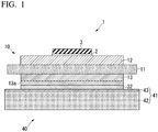
- Fig. 1 illustrates an insulating circuit board with a heatsink 40 manufactured using a method of manufacturing an insulating circuit board with a heatsink according to the embodiment of the present invention and a power module 1 in which the insulating circuit board with a heatsink 40 is used.
- the power module 1 illustrated in Fig. 1 includes: an insulating circuit board 10; a semiconductor element 3 that is bonded to a first surface (in Fig. 1 , an upper surface) of the insulating circuit board 10 via a solder layer 2; and a heatsink 41 that is bonded to a lower side of the insulating circuit board 10.
- the insulating circuit board 10 to which the heatsink 41 is bonded is the insulating circuit board with a heatsink 40 according to the embodiment.
- the semiconductor element 3 is formed of a semiconductor material such as Si.
- the solder layer 2 via the insulating circuit board 10 and the semiconductor element 3 are bonded is formed of, for example, a Sn-Ag solder material, a Sn-Cu solder material, a Sn-In solder material, or a Sn-Ag-Cu solder material (so-called lead-free solder material).
- the insulating circuit board 10 includes: a ceramic substrate 11 that is an insulating layer; a circuit layer 12 that is provided on a first surface (in Fig. 1 , an upper surface) of the ceramic substrate 11; and a metal layer 13 that is formed on a second surface (in Fig. 1 , a lower surface) of the ceramic substrate 11.
- the ceramic substrate 11 prevents electrical connection between the circuit layer 12 and the metal layer 13 and may be formed of aluminum nitride (AlN), silicon nitride (Si3N 4 ), or alumina (Al 2 O3) having high insulating properties.
- the ceramic substrate 11 is formed of aluminum nitride.
- the thickness of the ceramic substrate 11 is set to be in a range of 0.2 mm to 1.5 mm and, in the embodiment, may set to 0.635 mm.
- the circuit layer 12 is formed by bonding a metal sheet having conductivity to the first surface of the ceramic substrate 11.
- the circuit layer 12 is formed by bonding an aluminum sheet 22 formed of aluminum or an aluminum alloy.
- the aluminum sheet 22 forming the circuit layer 12 a rolled sheet of aluminum (2N aluminum) having a purity of 99 mass% or higher or an aluminum alloy such as A3003 or A6063 is used.
- a circuit pattern is formed on the circuit layer 12, and a first surface (in Fig. 1 , an upper surface) of the circuit layer 12 is a mounting surface on which the semiconductor element 3 is mounted.
- the thickness of the circuit layer 12 is set to be in a range of 0.1 mm to 2.0 mm and, in the embodiment, is set to 0.4 mm.
- the metal layer 13 is formed by bonding an aluminum sheet 23 formed of aluminum to the second surface of the ceramic substrate 11, laminating a clad material 51 on the second surface of the aluminum sheet 23, and heating the laminate.
- the indentation hardness in a thickness center portion of the metal layer 13 is lower than 50 mgf/ ⁇ m 2 .
- the indentation hardness is a value of the insulating circuit board with a heatsink 40 at 25°C.
- aluminum sheet 23 forming the metal layer 13 for example, aluminum (2N aluminum) having a purity of 99 mass% or higher, aluminum (3N aluminum) having a purity of 99.9 mass% or higher, or aluminum (4N aluminum) having a purity of 99.99 mass% or higher can be used.
- a rolled sheet of aluminum (4N aluminum) having a purity of 99.99 mass% or higher is used as the aluminum sheet 23 forming the metal layer 13.
- a thickness t0 of the metal layer 13 is set to be in a range of 0.2 mm to 1.0 mm and, in the embodiment, is set to 0.4 mm.
- a high alloy element concentration portion 13a having a higher alloy element concentration than a thickness center portion of the metal layer 13 and having a solidus temperature of 650°C or lower is formed in a region of the metal layer 13 opposite to the ceramic substrate 11.
- an alloy element concentration distribution is present in a thickness direction.
- the high alloy element concentration portion 13a is a region including Si and Mn as the alloy elements, in which a Si concentration is in a range of 2.0 mass% to 7.0 mass% and an Mn concentration is in a range of 0.3 mass% to 1.5 mass%.
- a thickness t1 of the high alloy element concentration portion 13a is preferably in a range of 0.05 mm to 0.3 mm.
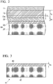
- the heatsink 41 is provided to cool the insulating circuit board 10 and, in the embodiment, is a radiating sheet formed of a material having excellent thermal conductivity as illustrated in Fig. 1 .
- the heatsink 41 is formed of an Al-SiC composite material (so-called AlSiC) of a porous body formed of SiC and an aluminum material formed of an aluminum alloy impregnated into the porous body.
- AlSiC Al-SiC composite material
- ADC12 solidus temperature: 570°C
- a skin layer 43 formed of an aluminum material (in the embodiment, ADC12) impregnated into a porous body is formed on a surface of a heatsink main body 42 formed of AlSiC.
- the thickness of the heatsink main body 42 is set to be in a range of 0.5 mm to 5.0 mm, and a thickness ts of a skin layer 43 is preferably 0.01 times to 0.1 times the thickness of the heatsink main body 42.
- a temperature difference between the solidus temperature of the high alloy element concentration portion 13a and the solidus temperature of the aluminum alloy forming the bonding surface (in the embodiment, the skin layer 43) of the heatsink 41 is in a range of 80°C or lower.
- the metal layer 13 of the insulating circuit board 10 and the heatsink 41 are bonded to each other via a copper bonding layer 32.
- the copper bonding layer 32 is formed of copper or a copper alloy.
- the copper bonding layer 32 is formed by bonding a copper sheet 52 formed of a rolled sheet of oxygen free copper.
- a thickness tc of the copper bonding layer 32 is set to be in a range of 0.05 mm to 5.0 mm.
- the metal layer 13 (high alloy element concentration portion 13a) and the copper bonding layer 32 are bonded to each other and the copper bonding layer 32 and the heatsink 41 (skin layer 43) are bonded to each other by solid phase diffusion bonding.
- the aluminum sheets 22 and 23 are laminated on the first surface and the second surface of the ceramic substrate 11 via brazing materials 26 and 27.
- the brazing materials 26 and 27 an A1-Si brazing material or an Al-Si-Mg brazing material is preferably used.
- the clad material 51 is laminated on the second surface side (in Fig.5 , the lower side) of the aluminum sheet 23 forming the metal layer 13.
- the clad material 51 includes: a core material 51a and a brazing material layer 51b that is formed on both surfaces of the core material 51a.
- the core material 51a is formed of an A3003 alloy
- the brazing material layer 51b is formed of an A4045 alloy.
- a ratio tb/ta of a thickness ta of the core material 51a and a thickness tb of the brazing material layer 51b in the clad material 51 is set to be in a range of 0.1 to 0.3.
- the laminate is heated.
- the ceramic substrate 11 and the aluminum sheets 22 and 23 are bonded to each other to form the circuit layer 12 and the metal layer 13, and the alloy elements of the brazing material layer 51b of the clad material 51 are diffused to the core material 51a and the aluminum sheet 23 side.
- the high alloy element concentration portion 13a having a higher alloy element concentration than the thickness center portion of the metal layer 13 and having a solidus temperature of 650°C or lower is formed in the region of the metal layer 13 opposite to the ceramic substrate 11.
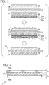
- the circuit layer and metal layer forming step S01 and the high alloy element concentration portion forming step S02 are performed at once.
- Bonding conditions in the circuit layer and metal layer forming step S01 and the high alloy element concentration portion forming step S02 are preferably set as follows: the atmosphere is a vacuum, the pressurization load is in a range of 0.1 MPa to 3.5 MPa, the heating temperature is in a range of 560°C to 630°C, and the holding time is in a range of 15 min to 60 min. In order to control the diffused state of the alloy elements, it is preferable that the bonding temperature and the holding time are adjusted in the above-described range.
- the insulating circuit board 10 according to the embodiment is formed.
- the heatsink 41 is laminated on the second surface side (in Fig. 7 , the lower side) of the metal layer 13 where the high alloy element concentration portion 13a is formed via the copper sheet 52 as a copper bonding material formed of a rolled sheet of oxygen free copper.
- the heatsink 41 is laminated such that the skin layer 43 faces the copper sheet 52 side.
- the insulating circuit board 10, the insulating circuit board 10 where the high alloy element concentration portion 13a is formed, the copper sheet 52, and the heatsink 41 are pressurized in the laminating direction and heated.
- the high alloy element concentration portion 13a of the metal layer 13 and the copper sheet 52 are bonded to each other and the copper sheet 52 and the heatsink 41 (skin layer 43) are bonded to each other by solid phase diffusion bonding.
- the load in the laminating direction is set to be in a range of 0.6 MPa to 3.5 MPa.
- the bonding temperature is in a range of 460°C to 540°C and preferably in a range of 480°C to 520°C.
- the holding time is in a range of 30 min to 240 min.
- the insulating circuit board with a heatsink 40 according to the embodiment is manufactured.
- the semiconductor element 3 is laminated on the circuit layer 12 of the insulating circuit board with a heatsink 40 via a solder material, and the circuit layer 12 of the insulating circuit board with a heatsink 40 and the semiconductor element 3 are bonded to each other in a reducing furnace.
- the power module 1 illustrated in Fig. 1 is manufactured as described above.
- the method of manufacturing the insulating circuit board with a heatsink 40 includes: the high alloy element concentration portion forming step S02 of forming the high alloy element concentration portion 13a having a higher alloy element concentration than the thickness center portion of the metal layer 13 and having a solidus temperature of 650°C or lower in the region of the metal layer 13 opposite to the ceramic substrate 11; and the heatsink bonding step S03 of bonding the heatsink 41 to the metal layer 13 by laminating the copper sheet 52 formed of copper or a copper alloy between the high alloy element concentration portion 13a of the metal layer 13 and a bonding surface (in the embodiment, the skin layer 43) of the heatsink 41 and bonding the high alloy element concentration portion 13a of the metal layer 13 and the copper sheet 52 to each other and bonding the copper sheet 52 and the heatsink 41 to each other by solid phase diffusion bonding.
- a temperature difference between the solidus temperature of the high alloy element concentration portion 13a of the metal layer 13 and the solidus temperature of aluminum or the aluminum alloy forming the bonding surface (in the embodiment, the skin layer 43) of the heatsink 41 can be reduced, even when solid phase diffusion bonding is performed under a relatively low-temperature condition, Al of the high alloy element concentration portion 13a of the metal layer 13 and Cu of the copper sheet 52 can be sufficiently diffused, Cu of the copper sheet 52 and Al of the bonding surface of the heatsink 41 can be sufficiently diffused, and the insulating circuit board 10 and the heatsink 41 can be reliably bonded to each other.
- the metal layer 13 is formed of aluminum (in the embodiment, 4N aluminum), and the indentation hardness in the thickness center portion of the metal layer 13 is lower than 50 mgf/ ⁇ m 2 . Therefore, during loading of a thermal cycle on the insulating circuit board with a heatsink 40, a thermal strain can be released by deforming the metal layer 13, and the cracking or the like of the ceramic substrate 11 can be suppressed.
- the heatsink 41 is formed of an Al-SiC composite material (so-called AlSiC) of a porous body formed of SiC and an aluminum material formed of an aluminum alloy impregnated into the porous body.
- AlSiC Al-SiC composite material
- ADC12 solidus temperature: 570°C
- the high alloy element concentration portion 13a is formed by laminating the clad material 51 including the core material 51a and the brazing material layer 51b formed on both surfaces of the core material 51a on the surface of the metal layer 13 opposite to the ceramic substrate 11 to obtain a laminate and heating the laminate to diffuse the alloy element of the brazing material layer 51b.
- the high alloy element concentration portion 13a having a higher alloy element concentration than the thickness center portion of the metal layer 13 and having a solidus temperature of 650°C or lower can be reliably formed in the region of the metal layer 13 opposite to the ceramic substrate 11.
- the ratio tb/ta of the thickness tb of the brazing material layer 51b to the thickness ta of the core material 51a in the clad material 51 used in the high alloy element concentration portion forming step S02 is set to be in a range of 0.1 to 0.3.
- the high alloy element concentration portion 13a having a higher alloy element concentration than the thickness center portion of the metal layer 13 and having a solidus temperature of 650°C or lower can be reliably formed in the region of the metal layer 13 opposite to the ceramic substrate 11.
- a temperature difference between the solidus temperature of the high alloy element concentration portion 13a of the metal layer 13 and the solidus temperature of the aluminum alloy forming the bonding surface (in the embodiment, the skin layer 43) of the heatsink 41 is in a range of 0°C to 80°C. Therefore, in the heatsink bonding step S03, even when solid phase diffusion bonding is performed under a relatively low-temperature condition, Al of the metal layer 13 (high alloy element concentration portion 13a) and Cu of the copper sheet 52 can be sufficiently diffused, Cu of the copper sheet 52 and Al of the bonding surface of the heatsink 41 can be sufficiently diffused, and the insulating circuit board 10 and the heatsink 41 can be reliably bonded to each other by solid phase diffusion bonding.
- the ceramic substrate 11 aluminum nitride (A1N) is used as the ceramic substrate 11, but the present invention is not limited thereto.
- the ceramic substrate 11 may be formed of another ceramic such as alumina (Al 2 O 3 ) or silicon nitride (Si 3 N 4 ).
- an insulating resin may be used.
- the heatsink may be a cooler including a passage through which a cooling medium passes.
- the heatsink is formed of an Al-SiC composite material (so-called AlSiC) in which an aluminum material formed of ADC12 impregnated into a porous body formed of SiC, but the present invention is not limited thereto.
- the material or structure of the bonding surface of the heatsink is not limited as long as the bonding surface of the heatsink is formed of an aluminum alloy having a solidus temperature of 650°C or lower.
- the circuit layer is formed of aluminum or an aluminum alloy, but the present invention is not limited thereto.
- the circuit layer may be formed of another metal such as copper or a copper alloy, or may have a structure in which an aluminum layer formed of aluminum or an aluminum alloy and a copper layer formed of copper or a copper alloy are laminated.
- the high alloy element concentration portion is formed by laminating the clad material on the metal layer and heating the laminate.
- the means of the high alloy element concentration portion forming step is not particularly limited.
- an insulating circuit board 110 or an insulating circuit board with a heatsink 140 may be configured in which the circuit layer 112 includes an aluminum layer 112A that is formed on the ceramic substrate 11 side as the insulating layer side and a copper layer 112B that is laminated on the aluminum layer 112A, and a second high alloy element concentration portion 112C having a higher alloy element concentration than a thickness center portion of the aluminum layer 112A and a solidus temperature of 650°C or lower is formed in a region of the aluminum layer 112A opposite to the ceramic substrate 11.
- the insulating circuit board with a heatsink 140 also includes the metal layer 13, the aluminum bonding layer 31, the copper bonding layer 32, and the heatsink 41.
- the insulating circuit board with a heatsink 140 illustrated in Fig. 8 is manufactured as follows.
- an aluminum sheet 122A that is an aluminum layer is laminated on the first surface (in Fig. 10 , the upper surface) of the ceramic substrate 11 via a brazing material 126, and the clad material 51 is laminated on a first surface of the aluminum sheet 122A.
- the aluminum sheet 23 that is the metal layer 13 is laminated on the second surface (in Fig. 10 , the lower surface) of the ceramic substrate 11 via a brazing material 127, and the clad material 51 is laminated on the second surface of the aluminum sheet 23.
- the aluminum sheet 122A that is the aluminum layer 112A and the aluminum sheet 23 that is the metal layer 13 are formed of, for example, aluminum (4N aluminum) having a purity of 99.99 mass% or higher or aluminum (2N aluminum) having a purity of 99 mass% or higher.
- brazing materials 126 and 127 are formed of an Al-Si-Mg alloy.
- the laminate is heated.
- the ceramic substrate 11 and the aluminum sheets 122A and 23 are bonded to each other to form the aluminum layer 112A and the metal layer 13.
- the alloy elements of the brazing material layer 51b of the clad material 51 are diffused to the core material 51a and the aluminum sheet 122A side.
- the second high alloy element concentration portion 112C having a higher alloy element concentration than the thickness center portion of the aluminum layer 112A and having a solidus temperature of 650°C or lower is formed in a region of the aluminum layer 112A opposite to the ceramic substrate 11.
- the alloy elements of the brazing material layer 51b of the clad material 51 are diffused to the core material 51a and the aluminum sheet 23 side.
- the high alloy element concentration portion 13a having a higher alloy element concentration than the thickness center portion of the metal layer 13 and having a solidus temperature of 650°C or lower is formed in the region of the metal layer 13 opposite to the ceramic substrate 11.
- Bonding conditions are preferably set as follows: the atmosphere is a vacuum, the pressurization load is in a range of 0.1 MPa to 3.5 MPa, and the heating temperature is in a range of 600°C to 640°C.
- the copper sheet 122B that is the copper layer 112B is laminated on the first surface (in Fig. 11 , the upper side) of the aluminum layer 112A where the second high alloy element concentration portion 112C is formed.
- the heatsink 41 is laminated on the second surface side (in Fig. 11 , the lower side) of the metal layer 13 where the high alloy element concentration portion 13a is formed via the copper sheet 52 as a copper bonding material formed of a rolled sheet of oxygen free copper.
- the heatsink 41 is laminated to form a laminate such that the skin layer 43 faces the copper sheet 52 side.
- the laminate is pressurized in the laminating direction and heated such that the aluminum layer 112A (the second high alloy element concentration portion 112C) and the copper sheet 122B are bonded to each other, the metal layer 13 (the high alloy element concentration portion 13a) and the copper sheet 52 are bonded to each other, and the copper sheet 52 and the heatsink 41 (the skin layer 43) are bonded to each other by solid phase diffusion bonding.
- the load in the laminating direction is set to be in a range of 0.6 MPa to 3.5 MPa.
- the bonding temperature is in a range of 460°C to 540°C and preferably in a range of 480°C to 520°C.
- the holding time is preferably in a range of 30 min to 240 min.
- the insulating circuit board with a heatsink 140 illustrated in Fig. 8 is manufactured.
- a circuit layer (37 mm ⁇ 37 mm ⁇ thickness 0.4 mm) formed of aluminum (4N aluminum) having a purity of 99.99 mass% was formed on a first surface of a ceramic substrate (40 mmx40 mmxthickness 0.635 mm) formed of aluminum nitride (AlN).
- a metal layer (37 mm ⁇ 37 mm) formed of a material shown in Table 1 and having a thickness shown in Table 1 was formed on a second surface of the ceramic substrate.
- the ceramic substrate and the aluminum sheet as the circuit layer and the metal layer were bonded to each other using an Al-7.5 mass% Si-0.01 mass% Mg brazing material foil (thickness: 15 ⁇ m).
- a clad material having a structure shown in Table 1 was laminated on a surface of the aluminum sheet as the metal layer opposite to the ceramic substrate.
- the laminate was heated under conditions shown in Table 1.
- a heatsink (50 mm ⁇ 60 mm ⁇ thickness 5.0 mm/thickness of skin layer: 0.1 mm) formed of an Al-SiC composite material (so-called AlSiC) in which aluminum having a solidus temperature shown in Table 1 was impregnated into a porous body of SiC was laminated on the metal layer via a copper bonding material (rolled sheet of oxygen free copper: 37 mm ⁇ 37 mm ⁇ thickness 1.0 mm).
- AlSiC Al-SiC composite material
- This laminate was pressurized in a laminating direction at 21 MPa and was held at 490°C for 150 min such that the metal layer where the high alloy element concentration portion was formed and the copper bonding material were bonded to each other and the copper bonding material and the heatsink were bonded to each other by solid phase diffusion bonding.
- the obtained insulating circuit board with a heatsink was evaluated for the respective items in the following order.
- the indentation hardness of the metal layer of the insulating circuit board with a heatsink was measured using a nanoindentation method. The measurement was performed at 10 positions of the center of the metal layer in the thickness direction to obtain the average value.
- a load-displacement relation was measured when a negative pressure was applied at a test load of 5000 mgf using a triangular pyramidal diamond indenter called a Berkovich indenter having a dihedral angle of 114.8° to 115.1°.
- exfoliation is represented by a white portion in the bonding layer. Therefore, the area of the white portion was set as the exfoliation area.
- Example 1 3 Metal Layer Clad Material Bonding Conditions Core Material Brazing Material Layer tb/ta Material Indentation Hardness (mgf/ ⁇ m) Thickness t0 (mm) Material Thickness Ta(mm) Material Thickness tb (mm) Pressurization Pressure (MPa) Holding Temperature (°C) Holding Temperature (min)
- Example 1 4N-Al 35 0.60 A3003 0.10 Al-Si-Mg 0.018 0.18 0.5 630 20
- Example 2 4N-Al 42 0.40 A3003 0.10 Al-Si-Mg 0.018 0.18 0.5 630 20
- Example 3 4N-A1 43 0.40 A3003 0.10 A4343 0.018 0.18 0.5 630 20
- Example 5 4N-Al 45 0.40 A3003 0.10 A4005 0.018 0.18 0.5 630 20
- Example 6 4N-A1 44 0.
- the present invention can provide a method of manufacturing an insulating circuit board with a heatsink in which a metal layer and a heatsink can be reliably bonded to each other by solid phase diffusion bonding even when the metal layer is formed of aluminum having a relatively low deformation resistance and a bonding surface of the heatsink is formed of an aluminum alloy having a relatively low solidus temperature.
- the present invention can provide a method of manufacturing an insulating circuit board with a heatsink in which a metal layer and a heatsink can be reliably bonded to each other by solid phase diffusion bonding even when the metal layer is formed of aluminum having a relatively low deformation resistance and a bonding surface of the heatsink is formed of an aluminum alloy having a relatively low solidus temperature.
Landscapes
- Engineering & Computer Science (AREA)
- Chemical & Material Sciences (AREA)
- Condensed Matter Physics & Semiconductors (AREA)
- General Physics & Mathematics (AREA)
- Physics & Mathematics (AREA)
- Computer Hardware Design (AREA)
- Microelectronics & Electronic Packaging (AREA)
- Power Engineering (AREA)
- Materials Engineering (AREA)
- Ceramic Engineering (AREA)
- Manufacturing & Machinery (AREA)
- Structural Engineering (AREA)
- Organic Chemistry (AREA)
- Cooling Or The Like Of Semiconductors Or Solid State Devices (AREA)
- Pressure Welding/Diffusion-Bonding (AREA)
- Mechanical Engineering (AREA)
Applications Claiming Priority (2)
| Application Number | Priority Date | Filing Date | Title |
|---|---|---|---|
| JP2018059917A JP6911805B2 (ja) | 2018-03-27 | 2018-03-27 | ヒートシンク付き絶縁回路基板の製造方法 |
| PCT/JP2019/012703 WO2019189090A1 (ja) | 2018-03-27 | 2019-03-26 | ヒートシンク付き絶縁回路基板の製造方法 |
Publications (3)
| Publication Number | Publication Date |
|---|---|
| EP3780088A1 true EP3780088A1 (de) | 2021-02-17 |
| EP3780088A4 EP3780088A4 (de) | 2022-01-05 |
| EP3780088B1 EP3780088B1 (de) | 2023-10-25 |
Family
ID=68061671
Family Applications (1)
| Application Number | Title | Priority Date | Filing Date |
|---|---|---|---|
| EP19777648.7A Active EP3780088B1 (de) | 2018-03-27 | 2019-03-26 | Verfahren zur herstellung einer isolierenden leiterplatte mit kühlkörper |
Country Status (7)
| Country | Link |
|---|---|
| US (1) | US11355408B2 (de) |
| EP (1) | EP3780088B1 (de) |
| JP (1) | JP6911805B2 (de) |
| KR (1) | KR102392568B1 (de) |
| CN (1) | CN111801790B (de) |
| TW (1) | TWI765145B (de) |
| WO (1) | WO2019189090A1 (de) |
Family Cites Families (18)
| Publication number | Priority date | Publication date | Assignee | Title |
|---|---|---|---|---|
| US6033787A (en) | 1996-08-22 | 2000-03-07 | Mitsubishi Materials Corporation | Ceramic circuit board with heat sink |
| JP3171234B2 (ja) * | 1997-03-26 | 2001-05-28 | 三菱マテリアル株式会社 | ヒートシンク付セラミック回路基板 |
| JP3468358B2 (ja) | 1998-11-12 | 2003-11-17 | 電気化学工業株式会社 | 炭化珪素質複合体及びその製造方法とそれを用いた放熱部品 |
| KR20110124372A (ko) * | 2004-04-05 | 2011-11-16 | 미쓰비시 마테리알 가부시키가이샤 | Al/AlN 접합체, 전력 모듈용 기판 및 전력 모듈, 그리고 Al/AlN 접합체의 제조 방법 |
| CN101849445B (zh) * | 2007-11-06 | 2012-11-21 | 三菱综合材料株式会社 | 陶瓷基板、陶瓷基板的制造方法和电源模块用基板的制造方法 |
| JP3171234U (ja) | 2011-08-09 | 2011-10-20 | 正宜 田辺 | 簡易温室 |
| JP5935292B2 (ja) * | 2011-11-01 | 2016-06-15 | 三菱マテリアル株式会社 | パワーモジュール用基板の製造方法、ヒートシンク付パワーモジュール用基板の製造方法 |
| JP2013229579A (ja) * | 2012-03-30 | 2013-11-07 | Mitsubishi Materials Corp | パワーモジュール用基板、ヒートシンク付パワーモジュール用基板及びパワーモジュール |
| JP5991102B2 (ja) | 2012-09-14 | 2016-09-14 | 三菱マテリアル株式会社 | ヒートシンク付パワーモジュール用基板、ヒートシンク付パワーモジュール、及びヒートシンク付パワーモジュール用基板の製造方法 |
| JP6621076B2 (ja) * | 2013-03-29 | 2019-12-18 | 三菱マテリアル株式会社 | パワーモジュール用基板、ヒートシンク付パワーモジュール用基板及びパワーモジュール |
| US10068829B2 (en) | 2014-04-25 | 2018-09-04 | Mitsubishi Materials Corporation | Power-module substrate unit and power module |
| JP6432208B2 (ja) * | 2014-08-18 | 2018-12-05 | 三菱マテリアル株式会社 | パワーモジュール用基板の製造方法、及び、ヒートシンク付パワーモジュール用基板の製造方法 |
| JP6432466B2 (ja) * | 2014-08-26 | 2018-12-05 | 三菱マテリアル株式会社 | 接合体、ヒートシンク付パワーモジュール用基板、ヒートシンク、接合体の製造方法、ヒートシンク付パワーモジュール用基板の製造方法、及び、ヒートシンクの製造方法 |
| JP6696214B2 (ja) * | 2015-04-16 | 2020-05-20 | 三菱マテリアル株式会社 | 接合体、ヒートシンク付パワーモジュール用基板、ヒートシンク、及び、接合体の製造方法、ヒートシンク付パワーモジュール用基板の製造方法、ヒートシンクの製造方法 |
| JP6822247B2 (ja) * | 2016-03-25 | 2021-01-27 | 三菱マテリアル株式会社 | ヒートシンク付絶縁回路基板の製造方法 |
| JP6750422B2 (ja) * | 2016-09-16 | 2020-09-02 | 三菱マテリアル株式会社 | 絶縁回路基板の製造方法、及び、絶縁回路基板、パワーモジュール、ledモジュール、熱電モジュール |
| KR102559200B1 (ko) | 2016-10-05 | 2023-07-25 | 삼성전자주식회사 | 배터리 유닛을 관리하는 장치, 방법, 및 시스템 |
| US11735434B2 (en) | 2017-03-29 | 2023-08-22 | Mitsubishi Materials Corporation | Method for producing insulating circuit substrate with heat sink |
-
2018
- 2018-03-27 JP JP2018059917A patent/JP6911805B2/ja active Active
-
2019
- 2019-03-26 KR KR1020207027511A patent/KR102392568B1/ko active IP Right Grant
- 2019-03-26 US US16/980,054 patent/US11355408B2/en active Active
- 2019-03-26 CN CN201980016961.2A patent/CN111801790B/zh active Active
- 2019-03-26 EP EP19777648.7A patent/EP3780088B1/de active Active
- 2019-03-26 WO PCT/JP2019/012703 patent/WO2019189090A1/ja unknown
- 2019-03-27 TW TW108110600A patent/TWI765145B/zh active
Also Published As
| Publication number | Publication date |
|---|---|
| TW201943320A (zh) | 2019-11-01 |
| CN111801790A (zh) | 2020-10-20 |
| JP2019175915A (ja) | 2019-10-10 |
| US11355408B2 (en) | 2022-06-07 |
| JP6911805B2 (ja) | 2021-07-28 |
| KR20200135960A (ko) | 2020-12-04 |
| WO2019189090A1 (ja) | 2019-10-03 |
| TWI765145B (zh) | 2022-05-21 |
| US20210020536A1 (en) | 2021-01-21 |
| CN111801790B (zh) | 2024-03-29 |
| EP3780088A4 (de) | 2022-01-05 |
| KR102392568B1 (ko) | 2022-04-28 |
| EP3780088B1 (de) | 2023-10-25 |
Similar Documents
| Publication | Publication Date | Title |
|---|---|---|
| EP2978018B1 (de) | Verfahren zur herstellung eines strommodulsubstrats | |
| EP2833399B1 (de) | Leistungsmodulsubstrat, leistungsmodulsubstrat mit kühlkörper und leistungsmodul | |
| EP2980844B1 (de) | Substrat für leistungsmodule, substrat mit kühlkörper für leistungsmodule und leistungsmodul | |
| EP2978019B1 (de) | Verfahren zur herstellung eines verbundeten körpers und verfahren zur herstellung eines strommodulsubstrats | |
| EP1667508B1 (de) | Keramische leiterplatte, verfahren zu ihrer herstellung und power-modul | |
| EP2214201A1 (de) | Verfahren zur herstellung eines trägers für ein strommodul, träger für strommodul und strommodul | |
| EP3605601B1 (de) | Verfahren zur herstellung einer isolierten leiterplatte mit kühlkörper | |
| KR20150129720A (ko) | 접합체, 파워 모듈용 기판, 및 히트 싱크가 부착된 파워 모듈용 기판 | |
| EP3041044B1 (de) | Verbundkörper und leistungsmodulsubstrat | |
| JP4104253B2 (ja) | 基板一体型構造体 | |
| CN111225891B (zh) | 接合体及绝缘电路基板 | |
| EP3597341A1 (de) | Verfahren zur herstellung eines gebondeten körpers, verfahren zur herstellung einer isolierten leiterplatte und verfahren zur herstellung einer isolierten leiterplatte mit einem kühlkörper | |
| EP3355370B1 (de) | Led modul substrat, led modul, led modul substrat mit kühler, und herstellungsverfahren für led modul substrat | |
| EP3888836A1 (de) | Verbundkörper, an kühlkörper befestigte, isolierte leiterplatte und kühlkörper | |
| EP3780088B1 (de) | Verfahren zur herstellung einer isolierenden leiterplatte mit kühlkörper | |
| WO2016167217A1 (ja) | 接合体、ヒートシンク付パワーモジュール用基板、ヒートシンク、及び、接合体の製造方法、ヒートシンク付パワーモジュール用基板の製造方法、ヒートシンクの製造方法 | |
| EP3703116B1 (de) | Verbundener körper, isolierte platine mit kühlkörper und kühlkörper | |
| WO2022224949A1 (ja) | 銅/セラミックス接合体、および、絶縁回路基板 | |
| EP4159704A1 (de) | Kupfer/keramik verbundkörper und isolierte leiterplatte | |
| EP4331766A1 (de) | Kühlkörper und kühlkörperintegrierte isolierende leiterplatte | |
| JP2001077485A (ja) | セラミック基板と金属放熱器の接合構造 |
Legal Events
| Date | Code | Title | Description |
|---|---|---|---|
| STAA | Information on the status of an ep patent application or granted ep patent |
Free format text: STATUS: THE INTERNATIONAL PUBLICATION HAS BEEN MADE |
|
| PUAI | Public reference made under article 153(3) epc to a published international application that has entered the european phase |
Free format text: ORIGINAL CODE: 0009012 |
|
| STAA | Information on the status of an ep patent application or granted ep patent |
Free format text: STATUS: REQUEST FOR EXAMINATION WAS MADE |
|
| 17P | Request for examination filed |
Effective date: 20200907 |
|
| AK | Designated contracting states |
Kind code of ref document: A1 Designated state(s): AL AT BE BG CH CY CZ DE DK EE ES FI FR GB GR HR HU IE IS IT LI LT LU LV MC MK MT NL NO PL PT RO RS SE SI SK SM TR |
|
| AX | Request for extension of the european patent |
Extension state: BA ME |
|
| DAV | Request for validation of the european patent (deleted) | ||
| DAX | Request for extension of the european patent (deleted) | ||
| A4 | Supplementary search report drawn up and despatched |
Effective date: 20211207 |
|
| RIC1 | Information provided on ipc code assigned before grant |
Ipc: C04B 37/02 20060101ALI20211201BHEP Ipc: H01L 21/48 20060101ALI20211201BHEP Ipc: H01L 23/373 20060101ALI20211201BHEP Ipc: H01L 23/12 20060101ALI20211201BHEP Ipc: B23K 20/00 20060101ALI20211201BHEP Ipc: H01L 23/36 20060101AFI20211201BHEP |
|
| GRAP | Despatch of communication of intention to grant a patent |
Free format text: ORIGINAL CODE: EPIDOSNIGR1 |
|
| STAA | Information on the status of an ep patent application or granted ep patent |
Free format text: STATUS: GRANT OF PATENT IS INTENDED |
|
| INTG | Intention to grant announced |
Effective date: 20230222 |
|
| RIN1 | Information on inventor provided before grant (corrected) |
Inventor name: NAGATOMO, YOSHIYUKI Inventor name: KITAHARA, TAKESHI |
|
| GRAJ | Information related to disapproval of communication of intention to grant by the applicant or resumption of examination proceedings by the epo deleted |
Free format text: ORIGINAL CODE: EPIDOSDIGR1 |
|
| STAA | Information on the status of an ep patent application or granted ep patent |
Free format text: STATUS: REQUEST FOR EXAMINATION WAS MADE |
|
| GRAP | Despatch of communication of intention to grant a patent |
Free format text: ORIGINAL CODE: EPIDOSNIGR1 |
|
| STAA | Information on the status of an ep patent application or granted ep patent |
Free format text: STATUS: GRANT OF PATENT IS INTENDED |
|
| INTC | Intention to grant announced (deleted) | ||
| INTG | Intention to grant announced |
Effective date: 20230523 |
|
| GRAS | Grant fee paid |
Free format text: ORIGINAL CODE: EPIDOSNIGR3 |
|
| GRAA | (expected) grant |
Free format text: ORIGINAL CODE: 0009210 |
|
| STAA | Information on the status of an ep patent application or granted ep patent |
Free format text: STATUS: THE PATENT HAS BEEN GRANTED |
|
| AK | Designated contracting states |
Kind code of ref document: B1 Designated state(s): AL AT BE BG CH CY CZ DE DK EE ES FI FR GB GR HR HU IE IS IT LI LT LU LV MC MK MT NL NO PL PT RO RS SE SI SK SM TR |
|
| REG | Reference to a national code |
Ref country code: GB Ref legal event code: FG4D |
|
| REG | Reference to a national code |
Ref country code: CH Ref legal event code: EP |
|
| REG | Reference to a national code |
Ref country code: DE Ref legal event code: R096 Ref document number: 602019040144 Country of ref document: DE |
|
| REG | Reference to a national code |
Ref country code: IE Ref legal event code: FG4D |
|
| REG | Reference to a national code |
Ref country code: LT Ref legal event code: MG9D |
|
| REG | Reference to a national code |
Ref country code: NL Ref legal event code: MP Effective date: 20231025 |
|
| REG | Reference to a national code |
Ref country code: AT Ref legal event code: MK05 Ref document number: 1625568 Country of ref document: AT Kind code of ref document: T Effective date: 20231025 |
|
| PG25 | Lapsed in a contracting state [announced via postgrant information from national office to epo] |
Ref country code: NL Free format text: LAPSE BECAUSE OF FAILURE TO SUBMIT A TRANSLATION OF THE DESCRIPTION OR TO PAY THE FEE WITHIN THE PRESCRIBED TIME-LIMIT Effective date: 20231025 |
|
| PG25 | Lapsed in a contracting state [announced via postgrant information from national office to epo] |
Ref country code: GR Free format text: LAPSE BECAUSE OF FAILURE TO SUBMIT A TRANSLATION OF THE DESCRIPTION OR TO PAY THE FEE WITHIN THE PRESCRIBED TIME-LIMIT Effective date: 20240126 |
|
| PG25 | Lapsed in a contracting state [announced via postgrant information from national office to epo] |
Ref country code: IS Free format text: LAPSE BECAUSE OF FAILURE TO SUBMIT A TRANSLATION OF THE DESCRIPTION OR TO PAY THE FEE WITHIN THE PRESCRIBED TIME-LIMIT Effective date: 20240225 |
|
| PG25 | Lapsed in a contracting state [announced via postgrant information from national office to epo] |
Ref country code: LT Free format text: LAPSE BECAUSE OF FAILURE TO SUBMIT A TRANSLATION OF THE DESCRIPTION OR TO PAY THE FEE WITHIN THE PRESCRIBED TIME-LIMIT Effective date: 20231025 |
|
| PG25 | Lapsed in a contracting state [announced via postgrant information from national office to epo] |
Ref country code: AT Free format text: LAPSE BECAUSE OF FAILURE TO SUBMIT A TRANSLATION OF THE DESCRIPTION OR TO PAY THE FEE WITHIN THE PRESCRIBED TIME-LIMIT Effective date: 20231025 |
|
| PG25 | Lapsed in a contracting state [announced via postgrant information from national office to epo] |
Ref country code: ES Free format text: LAPSE BECAUSE OF FAILURE TO SUBMIT A TRANSLATION OF THE DESCRIPTION OR TO PAY THE FEE WITHIN THE PRESCRIBED TIME-LIMIT Effective date: 20231025 |
|
| PG25 | Lapsed in a contracting state [announced via postgrant information from national office to epo] |
Ref country code: LT Free format text: LAPSE BECAUSE OF FAILURE TO SUBMIT A TRANSLATION OF THE DESCRIPTION OR TO PAY THE FEE WITHIN THE PRESCRIBED TIME-LIMIT Effective date: 20231025 Ref country code: IS Free format text: LAPSE BECAUSE OF FAILURE TO SUBMIT A TRANSLATION OF THE DESCRIPTION OR TO PAY THE FEE WITHIN THE PRESCRIBED TIME-LIMIT Effective date: 20240225 Ref country code: GR Free format text: LAPSE BECAUSE OF FAILURE TO SUBMIT A TRANSLATION OF THE DESCRIPTION OR TO PAY THE FEE WITHIN THE PRESCRIBED TIME-LIMIT Effective date: 20240126 Ref country code: ES Free format text: LAPSE BECAUSE OF FAILURE TO SUBMIT A TRANSLATION OF THE DESCRIPTION OR TO PAY THE FEE WITHIN THE PRESCRIBED TIME-LIMIT Effective date: 20231025 Ref country code: BG Free format text: LAPSE BECAUSE OF FAILURE TO SUBMIT A TRANSLATION OF THE DESCRIPTION OR TO PAY THE FEE WITHIN THE PRESCRIBED TIME-LIMIT Effective date: 20240125 Ref country code: AT Free format text: LAPSE BECAUSE OF FAILURE TO SUBMIT A TRANSLATION OF THE DESCRIPTION OR TO PAY THE FEE WITHIN THE PRESCRIBED TIME-LIMIT Effective date: 20231025 Ref country code: PT Free format text: LAPSE BECAUSE OF FAILURE TO SUBMIT A TRANSLATION OF THE DESCRIPTION OR TO PAY THE FEE WITHIN THE PRESCRIBED TIME-LIMIT Effective date: 20240226 |
|
| PGFP | Annual fee paid to national office [announced via postgrant information from national office to epo] |
Ref country code: DE Payment date: 20240320 Year of fee payment: 6 |