EP3779477A2 - Rapid over-the-air production line test platform - Google Patents
Rapid over-the-air production line test platform Download PDFInfo
- Publication number
- EP3779477A2 EP3779477A2 EP20191147.6A EP20191147A EP3779477A2 EP 3779477 A2 EP3779477 A2 EP 3779477A2 EP 20191147 A EP20191147 A EP 20191147A EP 3779477 A2 EP3779477 A2 EP 3779477A2
- Authority
- EP
- European Patent Office
- Prior art keywords
- antenna array
- dut
- ota
- production line
- rapid
- Prior art date
- Legal status (The legal status is an assumption and is not a legal conclusion. Google has not performed a legal analysis and makes no representation as to the accuracy of the status listed.)
- Pending
Links
Images


Classifications
-
- H—ELECTRICITY
- H01—ELECTRIC ELEMENTS
- H01P—WAVEGUIDES; RESONATORS, LINES, OR OTHER DEVICES OF THE WAVEGUIDE TYPE
- H01P5/00—Coupling devices of the waveguide type
- H01P5/02—Coupling devices of the waveguide type with invariable factor of coupling
- H01P5/022—Transitions between lines of the same kind and shape, but with different dimensions
- H01P5/028—Transitions between lines of the same kind and shape, but with different dimensions between strip lines
-
- H—ELECTRICITY
- H01—ELECTRIC ELEMENTS
- H01Q—ANTENNAS, i.e. RADIO AERIALS
- H01Q19/00—Combinations of primary active antenna elements and units with secondary devices, e.g. with quasi-optical devices, for giving the antenna a desired directional characteristic
- H01Q19/10—Combinations of primary active antenna elements and units with secondary devices, e.g. with quasi-optical devices, for giving the antenna a desired directional characteristic using reflecting surfaces
- H01Q19/104—Combinations of primary active antenna elements and units with secondary devices, e.g. with quasi-optical devices, for giving the antenna a desired directional characteristic using reflecting surfaces using a substantially flat reflector for deflecting the radiated beam, e.g. periscopic antennas
-
- G—PHYSICS
- G01—MEASURING; TESTING
- G01R—MEASURING ELECTRIC VARIABLES; MEASURING MAGNETIC VARIABLES
- G01R29/00—Arrangements for measuring or indicating electric quantities not covered by groups G01R19/00 - G01R27/00
- G01R29/08—Measuring electromagnetic field characteristics
- G01R29/10—Radiation diagrams of antennas
-
- G—PHYSICS
- G01—MEASURING; TESTING
- G01R—MEASURING ELECTRIC VARIABLES; MEASURING MAGNETIC VARIABLES
- G01R31/00—Arrangements for testing electric properties; Arrangements for locating electric faults; Arrangements for electrical testing characterised by what is being tested not provided for elsewhere
- G01R31/28—Testing of electronic circuits, e.g. by signal tracer
- G01R31/282—Testing of electronic circuits specially adapted for particular applications not provided for elsewhere
- G01R31/2822—Testing of electronic circuits specially adapted for particular applications not provided for elsewhere of microwave or radiofrequency circuits
-
- H—ELECTRICITY
- H01—ELECTRIC ELEMENTS
- H01P—WAVEGUIDES; RESONATORS, LINES, OR OTHER DEVICES OF THE WAVEGUIDE TYPE
- H01P3/00—Waveguides; Transmission lines of the waveguide type
- H01P3/02—Waveguides; Transmission lines of the waveguide type with two longitudinal conductors
- H01P3/08—Microstrips; Strip lines
- H01P3/081—Microstriplines
- H01P3/082—Multilayer dielectric
-
- H—ELECTRICITY
- H01—ELECTRIC ELEMENTS
- H01P—WAVEGUIDES; RESONATORS, LINES, OR OTHER DEVICES OF THE WAVEGUIDE TYPE
- H01P3/00—Waveguides; Transmission lines of the waveguide type
- H01P3/02—Waveguides; Transmission lines of the waveguide type with two longitudinal conductors
- H01P3/08—Microstrips; Strip lines
- H01P3/088—Stacked transmission lines
-
- H—ELECTRICITY
- H01—ELECTRIC ELEMENTS
- H01P—WAVEGUIDES; RESONATORS, LINES, OR OTHER DEVICES OF THE WAVEGUIDE TYPE
- H01P5/00—Coupling devices of the waveguide type
- H01P5/02—Coupling devices of the waveguide type with invariable factor of coupling
-
- H—ELECTRICITY
- H01—ELECTRIC ELEMENTS
- H01Q—ANTENNAS, i.e. RADIO AERIALS
- H01Q13/00—Waveguide horns or mouths; Slot antennas; Leaky-waveguide antennas; Equivalent structures causing radiation along the transmission path of a guided wave
- H01Q13/02—Waveguide horns
-
- H—ELECTRICITY
- H01—ELECTRIC ELEMENTS
- H01Q—ANTENNAS, i.e. RADIO AERIALS
- H01Q15/00—Devices for reflection, refraction, diffraction or polarisation of waves radiated from an antenna, e.g. quasi-optical devices
- H01Q15/02—Refracting or diffracting devices, e.g. lens, prism
- H01Q15/06—Refracting or diffracting devices, e.g. lens, prism comprising plurality of wave-guiding channels of different length
-
- H—ELECTRICITY
- H01—ELECTRIC ELEMENTS
- H01Q—ANTENNAS, i.e. RADIO AERIALS
- H01Q15/00—Devices for reflection, refraction, diffraction or polarisation of waves radiated from an antenna, e.g. quasi-optical devices
- H01Q15/14—Reflecting surfaces; Equivalent structures
-
- H—ELECTRICITY
- H01—ELECTRIC ELEMENTS
- H01Q—ANTENNAS, i.e. RADIO AERIALS
- H01Q19/00—Combinations of primary active antenna elements and units with secondary devices, e.g. with quasi-optical devices, for giving the antenna a desired directional characteristic
- H01Q19/06—Combinations of primary active antenna elements and units with secondary devices, e.g. with quasi-optical devices, for giving the antenna a desired directional characteristic using refracting or diffracting devices, e.g. lens
-
- H—ELECTRICITY
- H01—ELECTRIC ELEMENTS
- H01Q—ANTENNAS, i.e. RADIO AERIALS
- H01Q19/00—Combinations of primary active antenna elements and units with secondary devices, e.g. with quasi-optical devices, for giving the antenna a desired directional characteristic
- H01Q19/10—Combinations of primary active antenna elements and units with secondary devices, e.g. with quasi-optical devices, for giving the antenna a desired directional characteristic using reflecting surfaces
- H01Q19/18—Combinations of primary active antenna elements and units with secondary devices, e.g. with quasi-optical devices, for giving the antenna a desired directional characteristic using reflecting surfaces having two or more spaced reflecting surfaces
- H01Q19/185—Combinations of primary active antenna elements and units with secondary devices, e.g. with quasi-optical devices, for giving the antenna a desired directional characteristic using reflecting surfaces having two or more spaced reflecting surfaces wherein the surfaces are plane
-
- H—ELECTRICITY
- H01—ELECTRIC ELEMENTS
- H01Q—ANTENNAS, i.e. RADIO AERIALS
- H01Q21/00—Antenna arrays or systems
- H01Q21/29—Combinations of different interacting antenna units for giving a desired directional characteristic
- H01Q21/293—Combinations of different interacting antenna units for giving a desired directional characteristic one unit or more being an array of identical aerial elements
-
- H—ELECTRICITY
- H04—ELECTRIC COMMUNICATION TECHNIQUE
- H04B—TRANSMISSION
- H04B17/00—Monitoring; Testing
-
- H—ELECTRICITY
- H04—ELECTRIC COMMUNICATION TECHNIQUE
- H04B—TRANSMISSION
- H04B17/00—Monitoring; Testing
- H04B17/0082—Monitoring; Testing using service channels; using auxiliary channels
- H04B17/0085—Monitoring; Testing using service channels; using auxiliary channels using test signal generators
-
- H—ELECTRICITY
- H01—ELECTRIC ELEMENTS
- H01Q—ANTENNAS, i.e. RADIO AERIALS
- H01Q3/00—Arrangements for changing or varying the orientation or the shape of the directional pattern of the waves radiated from an antenna or antenna system
- H01Q3/26—Arrangements for changing or varying the orientation or the shape of the directional pattern of the waves radiated from an antenna or antenna system varying the relative phase or relative amplitude of energisation between two or more active radiating elements; varying the distribution of energy across a radiating aperture
- H01Q3/267—Phased-array testing or checking devices
Definitions
- the present disclosure generally relates to production line test platforms. More specifically, the present disclosure relates to rapid millimeter wave (mmWave) fifth generation (5G) mobile communication over-the-air (OTA) production line test platforms.
- mmWave millimeter wave
- 5G fifth generation
- OTA mobile communication over-the-air
- 5G New Radio has re-defined a new frequency spectrum under the following three circumstances: enhanced Mobile Broadband (eMBB), Ultra-Reliable and Low Latency Communications (URLLC) and massive Machine Type Communications (mMTC).
- eMBB enhanced Mobile Broadband
- URLLC Ultra-Reliable and Low Latency Communications
- mMTC massive Machine Type Communications
- Frequency Range 2 (FR2) uses millimeter waves (mmWave) with frequencies range from 24250 MHz to 52600 MHz in 3GPP standard.
- mmWave millimeter waves
- beamforming technique has been employed in antenna arrays to achieve higher equivalent isotropically radiated power (EIRP) and wider coverage.
- antenna arrays can be integrated into RF modules.
- a high density module is called an Antennas in Package (AiP) module and can be mass produced.
- AiP Antennas in Package
- the present disclosure provides a rapid over-the-air (OTA) production line test platform, which may include: an antenna array for transmitting a test beam in a plurality of transmitting directions; an electromagnetic wave guiding device for guiding the test beam; a test machine to be loaded with a device under test (DUT) for controlling the DUT to receive the guided test beam from a plurality of receiving directions; and a controller electrically connected with the test machine and the antenna array for calculating an antenna radiation pattern of the DUT based on at least one power received from the plurality of receiving directions corresponding to the DUT and a transmitting power of the antenna array.
- OTA over-the-air
- the rapid OTA production line test platform may further include: two reflecting plates disposed opposite to each other and between the DUT and the antenna array, wherein the test beam propagates between the antenna array, the DUT and the two reflecting plates to enable an OTA beam test of the DUT.
- the rapid OTA production line test platform may further include a first horn antenna array and a second horn antenna array arranged and focus around a first center and a second center, respectively; and a plurality of bending waveguides connected between the first horn antenna array and the second horn antenna array, wherein the antenna array at the first center sequentially transmits the test beam with beamforming towards the first horn antenna array, and the DUT capable of beamforming at the second center receives the test beam after being guided by the plurality of bending waveguides to implement the OTA beam test of the DUT.
- the rapid OTA production line test platform may further include a three dimensional (3D) elliptic curve, wherein a plane of the antenna array and a plane of the DUT capable of beamforming are perpendicular to each other, and the test beam is transmitted with beamforming by the antenna array at a first focal point of the 3D elliptic curve, then reflected by the 3D elliptic curve and received by the DUT at a second focal point of the 3D elliptic curve to implement the OTA beam test of the DUT.
- 3D three dimensional
- an objective of the present disclosure is to provide a rapid over-the-air (OTA) production line test platform applicable to millimeter wave (mmWave) fifth generation (5G) mobile communication.
- OTA over-the-air
- mmWave millimeter wave
- 5G fifth generation
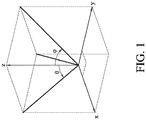
- a first component angle ⁇ is the angle of the projection of a transmitting vector on a xz plane with respect to the normal direction (z axis)
- a second component angle ⁇ is the angle of the projection of the transmitting direction of the electromagnetic wave on a yz plane with respect to the normal direction (z axis).
- the signal strength of a signal source (i.e., transmitting end) is represented as Ps, which varies with the first component angle ⁇ and the second component angle ⁇ .
- Ps the signal strength of a signal source
- the contour lines are not perfect circles, but rather the strengths of the transmitting signals may vary slightly with differences in the two component angles. This is a characteristic of antenna arrays.
- the signal strength of a signal source can be represented as P S ( ⁇ , ⁇ ), and the path loss can be represented as P L .
- path loss is a function of the path length R
- path loss can be essentially represented as P L (R).
- the noise signal strength at the receiving end i.e., the DUT
- P N is typically set as a constant for the same DUT.
- the noise signal strength is usually frequency-specific and the environment is assumed to be unchanged (in practice, however, the noise signal strength may still vary with frequency and the environment).
- the gain at the receiving end varies with the first component angle ⁇ and the second component angle ⁇ of the directional receiving angle (similar to the signal strength of the signal source)
- the gain at the receiving end can be expressed as G R ( ⁇ , ⁇ )
- the gain G R ( ⁇ , ⁇ ) at the receiving end can be obtained by measurement and calculation.
- the antenna radiation pattern of the DUT can then be obtained by a quantitative grid chart of a power level scan. In some applications, the energy can be computed directly.
- the DUT in the case that the DUT is an antenna array instead of a single antenna and the signal source is also an antenna array, the signal source emits mmWave to the DUT with a first component angle ⁇ m and a second component angle ⁇ n , then the DUT will also need to correspondingly switch to ⁇ m and ⁇ n , i.e., ( ⁇ m , ⁇ n ) .
- the signal source emits mmWave to the DUT with a first component angle ⁇ m and a second component angle ⁇ n , then the DUT will also need to correspondingly switch to ⁇ x and ⁇ y , i.e., ( ⁇ x , ⁇ y ), wherein x is m-2 ⁇ m+2, and y is n-2 ⁇ n+2, but the present disclosure is not limited as such.
- the SNRs received by the receiving ends can all be obtained by measurement and calculation (as mentioned above) in order to obtain the antenna radiation patterns of the DUTs via quantitative grid charts of a power level scan.
- the signal strength received by the DUT can be calculated directly and the antenna radiation pattern can be obtained using the equation (1) above.
- measuring and calculating the signal strength (power) received by the receiving end is substantially equivalent to the method realized using the SNR above.
- the notion of determining an antenna radiation pattern of a DUT from multiple directions is realized by an antenna array of known characteristics and an electromagnetic wave guiding device.
- the antenna array emits test beams in a plurality of transmitting directions, and the electromagnetic wave guiding device guides the test beams.
- a DUT is loaded on a test machine and controlled to receive the guided test beams from a plurality of receiving directions.
- a controller is electrically connected with the test machine and the antenna array for calculating the antenna radiation pattern of the DUT based on at least on the power received by the DUT at the plurality of receiving directions as well as the transmission power of the antenna array.
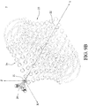
- FIGs. 3A to 3D are schematic diagrams depicting a rapid OTA production line test platform 1 in accordance with an embodiment of the present disclosure.
- the rapid OTA production line test platform 1 of the present disclosure for testing a device under test (DUT) 11 includes an antenna array 12, two reflecting plates 13 and a beamforming circuit 14.
- the electromagnetic wave guiding device substantially includes at least the two reflecting plates 13 above.
- the DUT 11 includes a beamforming function.
- the antenna array 12 is disposed opposite to the DUT 11 and emits test beams using a beamforming technique.
- the two reflecting plates 13 are disposed opposite to each other and between the DUT 11 and the antenna array 12. The OTA beam testing of the DUT 11 is conducted on beams reflected by the reflecting plates 13 at either side.
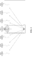
- the antenna array 12 is capable of beamforming, and the reflecting plates 13 at the two sides allows different beam directions of the DUT to be tested according to the needs. As shown in FIGs. 3A-3D , in an embodiment of the present disclosure, through direct transmission, single reflection, double reflections and triple reflections, 7 different sets of angles can be tested as can be seen in FIG. 4 .
- the path lengths of the present embodiment are related to the two component angles, so the path loss in this embodiment can be expressed as P L ( ⁇ , ⁇ ) .
- the gain of the DUT 11 i.e., the receiving end
- the gain of the DUT 11 at a specific receiving angle can be obtained based on the received SNR (or power) and other known parameters by measurements and calculations using the above equation (1), and data at various receiving angles can be collected to obtain the antenna radiation pattern of the DUT 11.
- the beamforming circuit 14 of the present disclosure can be connected to the antenna array 12. Since the beamforming circuit 14 includes a beamforming electronic scanning probe capable of 2D plane scan. Based on the requirements of the OTA tests, the beamforming circuit 14 can be connected to a network analyzer, signal generator, signal analyzer or a baseband equipment to perform other types of tests. Moreover, depending on the frequency band of the test equipment, an up/down frequency circuit with up/down frequency function can be added if needed.
- the rapid OTA production line test platform 2 of the present disclosure for testing a DUT 21 includes an antenna array 22, a first horn antenna array 23 a second horn antenna array 24 and a plurality of bending waveguides 25.
- the electromagnetic wave guiding device substantially includes at least the first horn antenna array 23, the second horn antenna array 24 and the plurality of bending waveguides 25.
- the DUT 21 is similarly capable of beamforming.
- the first horn antenna array 23 and the second horn antenna array 24 are arranged and focused around a first center C1 and a second center C2, respectively.
- the plurality of bending waveguides 25 are connected between the first horn antenna array 23 and the second horn antenna array 24.
- the antenna array 22 at the first center C1 sequentially emits signals towards the first horn antenna array 23, and the DUT 21 receives at the second center C2, so as to conduct OTA beam testing of the DUT 21.
- the first horn antenna array 23 and the second horn antenna array 24 of the present disclosure being arranged and focused around the two centers (i.e., the first center C1 and the second center C2) allows the antenna array 22 at the first center C1 to emit signals by beamforming techniques and the DUT 21 at the second center C2 (the other center) to beamformingly receive the signals through the first horn antenna array 23 and the second horn antenna array 24 coupled with the plurality of bending waveguides 25.
- the antenna array 22 acting as a transmitting end at the first center C1 can also be a receiving end, while the DUT 21 acting as a receiving end at the second center C2 can be a transmitting end. Therefore, transmitting and receiving radiation patterns can be measured.
- the resolution of the first horn antenna array 23 and the second horn antenna array 24 depends on the number of horn antennae in the first horn antenna array 23 and the second horn antenna array 24, the intervals between the horn antennae, and the distance between the DUT 21 and the first horn antenna array 23 and the second horn antenna array 24 as well as the distance between the antenna array 22 and the first horn antenna array 23 and the second horn antenna array 24.
- the plurality of bending waveguides 25 are used instead of the reflecting plates to guide the beamforming from the transmitting interface to the receiving interface at defined angles in order to obtain the measurements of beam peak power level and the phase.
- the path lengths in this embodiment are the path lengths of free space, i.e., the distance from the antenna array 22 of the transmitting end to the first horn antenna array 23 and the distance from the DUT 21 to the second horn antenna array 24.
- the plurality of bending waveguides 25 are assumed to have no path loss, so the path loss of the present embodiment can be set as a constant.
- the gain of the DUT 21 i.e., the receiving end
- the antenna radiation pattern of the DUT 21 can be obtained through a quantitative grid chart of a power level scan (as shown in FIG. 7 ).
- the path lengths in this embodiment can be represented by P L ( ⁇ , ⁇ ) .
- the path lengths of free space i.e., the distance from the antenna array 22 of the transmitting end to the first horn antenna array 23 and the distance from the DUT 21 to the second horn antenna array 24
- a compensation model needs to be introduced.
- FIG. 7 is a quantitative diagram depicting a power level scan of a S21 signal passing through a DUT (using 9 ⁇ 9 horn antenna arrays as an example).
- the transmitting end at the first center C1 sequentially transmits directional beamforming towards the 9 ⁇ 9 horn antenna arrays, and the receiving end at the second center C2 receives the beams at 0 degree of a fixed boresight along the positive Y axis.
- the present embodiment further includes a rotary motor 26 for rotating the DUT 21, thereby increasing the flexibility of its application.
- the present embodiment further includes a beamforming circuit (not shown) that can be connected to the antenna array 22.
- FIGs. 9A and 9B are schematic diagrams depicting a rotatable DUT 21. If the beam width of the DUT 21 is resolution ⁇ n+m (where n is an integer greater than or equal to 0, 0 ⁇ m ⁇ resolution, and m is an integer), then the DUT 21 can be made to direct its beams to the boresight of the transmitting end or at an angle that is an integer multiple of the resolution through the rotary motor 26 (e.g., such that the beams pointing to the opposite direction) to carry out measurements using the present embodiment.
- the directionality of the beams of the DUT 21 is -9 degrees rotation in the X-axis and -9 degrees rotation in the Z-axis
- the rotary motor 26 can rotate the antenna plane of the DUT 21 in the opposite direction to +9 degrees rotation in the X-axis and +9 degrees rotation in the Z-axis.
- the present embodiment employs horn antenna arrays arranged in circles combined with bending waveguides, such that the transmitting end and the receiving end can simultaneously perform 3D beamforming measurements.
- the present embodiment effectively reduces the time for beamforming verification and measurement, that is, by simply multiplying the beam switching time by the number of angle points required.
- the present embodiment requires only the use of bending waveguides and horn antenna arrays without the need for reflective planes or complex mechanical components, thereby effectively reducing the cost of measurement.
- FIG. 10 is a schematic diagram of a rapid OTA production line test platform 3 in accordance with an embodiment of present disclosure.
- the rapid OTA production line test platform 3 of the present disclosure for testing a DUT 31 includes an antenna array 32 and a 3D elliptic curve 33.
- the DUT 31 is capable of beamforming.
- the plane of the DUT 31 is perpendicular to the plane of the antenna array 32.
- the antenna array 32 is disposed at a second focal point F2 of the 3D elliptic curve 33 and emits beams by beamforming techniques, while the DUT 31 receives signals at a first focal point F1 of the 3D elliptic curve 33 through single reflection, such that OTA test of the DUT 31 can be achieved.
- the electromagnetic wave guiding device described before substantially includes at least the 3D elliptic curve 33.
- the present embodiment allows the antenna array 32 (i.e., the transmitting end) at the second focal point F2 to emit signals by beamforming techniques, and the DUT 31 at the other focal point (i.e., the first focal point F1) to receive the signals by beamforming techniques through single reflection, wherein the reflection angle can be computed from the incident angle and the 3D elliptic curve equation.
- the transmitting end at the second focal point F2 can also be used as a receiving end, while the receiving end at the first focal point F1 can be used as a transmitting end. Therefore, transmitting and receiving radiation patterns can be measured.
- the path lengths in this embodiment are all the same, and can thus be set as a constant.
- the gain of the DUT 31 at specific receiving angle and rotational direction can be obtained based on the received SNR (or power) and other known parameters by measurements and calculations using the equation (1) above, and the antenna radiation pattern of the DUT 31 can then be obtained through a quantitative grid chart of a power level scan.
- the path lengths in this embodiment can be expressed as P L ( ⁇ , ⁇ ) .
- the plane of the DUT 31 and the plane of the antenna array 32 are perpendicular to each other, so the plane of the DUT 31 vertical to the plane of the transmitting end allows the beamforming coverage area to be effectively utilized.
- the present embodiment further includes a beamforming circuit (not shown) that can be connected to the antenna array 32.
- the ratio of the long axis a to the short axis b of the 3D elliptic curve 33 is 1.3, and a 3D elliptic curve 33 with 1 ⁇ 4 of an area is used, the transmitting end and the receiving end can simultaneously perform beamforming measurements.
- the present embodiment effective shortens the beamforming verification and measurement time.
- the 3D elliptic curve 33 may also be a 3D elliptic reflective surface with 1/8 or other fractions of an area.
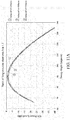
- FIG. 11A is the simulation result of a S21 power level scan (assuming 3D elliptic curve has 1 ⁇ 4 of an area, the ratio of the long axis a to the short axis b is 1.1, and the value of b is 250 mm, 500 mm, and 750 mm). As can be seen from the simulation result set forth in FIG. 11A , given that the ratios of the long axis a to the short axis b are unchanged, similar reflection characteristic can be obtained with different values of b.
- FIG. 11B is the simulation result of a S21 power level scan (assuming 3D elliptic curve has 1 ⁇ 4 of an area, the ratio of the long axis a to the short axis b is 1.3, and the value of b is 250 mm, 500 mm, and 750 mm). As can be seen from the simulation result set forth in FIG. 11B , given that the ratios of the long axis a to the short axis b are unchanged, similar reflection characteristic can still be obtained with different values of b.
- FIGs. 11A and 11B indicate power levels received by the DUT at a fixed angle of 90 degrees at the first focal point F1 scanned by beams at different incident angles (i.e., different sweep angles) from the second focal point F2.
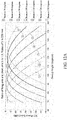
- FIG. 12A is the simulation result of a S21 power level scan (assuming 3D elliptic curve has 1 ⁇ 4 of an area, the ratio of the long axis a to the short axis b is 1.1, and the value of b is 250 mm).
- the angle of the power peak of the DUT is the transmitting angle at the originating focal point.
- FIG. 12B is the simulation result of a S21 power level scan (assuming 3D elliptic curve has 1 ⁇ 4 of an area, the ratio of the long axis a to the short axis b is 1.3, and the value of b is 250 mm).
- the angle of the power peak of the DUT is the transmitting angle at the originating focal point.
- FIGs. 12A and 12B indicate power levels received by the DUT at different beam angles (i.e., DUT sweep angles) at the first focal point F1 scanned by beams from the second focal point F2.
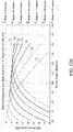
- FIG. 13 is the simulation result of a S21 power level scan (assuming 3D elliptic curve has 1 ⁇ 4 of an area and the value of b is 250 mm).
- different scan coverages resulted from different ratios (i.e., the ratio of long axis a to the short axis b); the larger the ratio, the lower the angle recognition rate; and on the other hand, the smaller the ratio, the higher the angle recognition rate.
- ratios 1.1 to 1.5 are used and a wider reflection range is obtained by increasing the curvature, then different application needs can be met.
- the present embodiment is able to realize rapid OTA testing through 3D elliptic curves or piecewise curves without the need for reflecting plates or complex mechanical components, thereby effectively reducing the cost of measurement.
- the various embodiments of the present disclosure described above includes the beamforming electronic probe for electronic scanning and reflective planes for DUT testing at different angles.
- electronic scanning is used by the present disclosure, it has significant improvements over the conventional mechanical scanning in terms of speed and precision.
- electronic probe is used in the present disclosure, there is the possibility for automated testing in overall OTA system integration.
Landscapes
- Physics & Mathematics (AREA)
- Electromagnetism (AREA)
- Engineering & Computer Science (AREA)
- Computer Networks & Wireless Communication (AREA)
- Signal Processing (AREA)
- General Physics & Mathematics (AREA)
- General Engineering & Computer Science (AREA)
- Variable-Direction Aerials And Aerial Arrays (AREA)
- Aerials With Secondary Devices (AREA)
- Structure Of Printed Boards (AREA)
- Production Of Multi-Layered Print Wiring Board (AREA)
- Microelectronics & Electronic Packaging (AREA)
- Support Of Aerials (AREA)
Abstract


Description
- The present disclosure generally relates to production line test platforms. More specifically, the present disclosure relates to rapid millimeter wave (mmWave) fifth generation (5G) mobile communication over-the-air (OTA) production line test platforms.
- The maturing of the fifth generation (5G) mobile communication technology has critically influenced in various application, such as vehicle-to-everything (V2X), edge computing, artificial intelligence of things (AIoT) in the next generation mobile communication technology. 5G New Radio (5G NR) has re-defined a new frequency spectrum under the following three circumstances: enhanced Mobile Broadband (eMBB), Ultra-Reliable and Low Latency Communications (URLLC) and massive Machine Type Communications (mMTC). Frequency Range 2 (FR2) uses millimeter waves (mmWave) with frequencies range from 24250 MHz to 52600 MHz in 3GPP standard. In order to overcome high path loss during signal transmission, beamforming technique has been employed in antenna arrays to achieve higher equivalent isotropically radiated power (EIRP) and wider coverage.
- Nowadays, antenna arrays can be integrated into RF modules. Such a high density module is called an Antennas in Package (AiP) module and can be mass produced. For mass-produced AiP modules, conventional conductivity tests are not capable of testing of large amounts of products and conducting fast product testing.
- Moreover, during product testing, traditional mechanical turntables have relatively slow testing speeds if high precision is required. On the other hand, if fast testing is needed, then precision may be compromised. If both high precision and fast testing are demanded, then the mechanical motors used will be considerably more expensive. As such, in the case of mass-produced products, traditional mechanical testing is not suitable for mass production testing.
- Therefore, there is a need in the art for a low-cost, high-performance rapid production line test platform to address the aforementioned shortcomings.
- The present disclosure provides a rapid over-the-air (OTA) production line test platform, which may include: an antenna array for transmitting a test beam in a plurality of transmitting directions; an electromagnetic wave guiding device for guiding the test beam; a test machine to be loaded with a device under test (DUT) for controlling the DUT to receive the guided test beam from a plurality of receiving directions; and a controller electrically connected with the test machine and the antenna array for calculating an antenna radiation pattern of the DUT based on at least one power received from the plurality of receiving directions corresponding to the DUT and a transmitting power of the antenna array.
- In an embodiment, the rapid OTA production line test platform may further include: two reflecting plates disposed opposite to each other and between the DUT and the antenna array, wherein the test beam propagates between the antenna array, the DUT and the two reflecting plates to enable an OTA beam test of the DUT.
- In an embodiment, the rapid OTA production line test platform may further include a first horn antenna array and a second horn antenna array arranged and focus around a first center and a second center, respectively; and a plurality of bending waveguides connected between the first horn antenna array and the second horn antenna array, wherein the antenna array at the first center sequentially transmits the test beam with beamforming towards the first horn antenna array, and the DUT capable of beamforming at the second center receives the test beam after being guided by the plurality of bending waveguides to implement the OTA beam test of the DUT.
- In an embodiment, the rapid OTA production line test platform may further include a three dimensional (3D) elliptic curve, wherein a plane of the antenna array and a plane of the DUT capable of beamforming are perpendicular to each other, and the test beam is transmitted with beamforming by the antenna array at a first focal point of the 3D elliptic curve, then reflected by the 3D elliptic curve and received by the DUT at a second focal point of the 3D elliptic curve to implement the OTA beam test of the DUT.
-
-
FIG. 1 is a schematic diagram depicting transmission and receiving by an antenna array. -
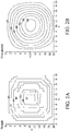
FIG. 2A is a schematic contour map depicting strengths of a power level scan. -
FIG. 2B is a schematic contour map depicting strengths of a power level scan (oversampled). -
FIGs. 3A to 3D are schematic diagrams depicting a rapid OTA production line test platform in accordance with a first embodiment of the present disclosure. -
FIG. 4 is a schematic diagram illustrating seven different sets of angles that can be tested in the rapid OTA production line test platform of the first embodiment of the present disclosure. -
FIG. 5 is a schematic perspective view of a rapid OTA production line test platform in accordance with a second embodiment of the present disclosure. -
FIG. 6 is a schematic side view of a rapid OTA production line test platform in accordance with the second embodiment of the present disclosure. -
FIG. 7 is a quantitative diagram of a S21 power level scan (using 9×9 horn antenna array as an example). -
FIG. 8 is a schematic perspective view of the rapid OTA production line test platform including a rotary motor in accordance with the second embodiment of the present disclosure. -
FIG. 9A is a schematic side view of a DUT rotated an angle in the rapid OTA production line test platform in accordance with the second embodiment of the present disclosure. -
FIG. 9B is a schematic perspective view of a DUT rotated an angle in the rapid OTA production line test platform in accordance with the second embodiment of the present disclosure. -
FIG. 10 is a schematic perspective view of a rapid OTA production line test platform in accordance with a third embodiment of the present disclosure. -
FIG. 11A is a graph depicting the simulation result of a S21 power level scan (assuming 3D elliptic curve has ¼ of an area, the ratio of a long axis a to a short axis b being 1.1, and the value of b being 250 mm, 500 mm, and 750 mm). -
FIG. 11B is a graph depicting the simulation result of a S21 power level scan (assuming 3D elliptic curve has ¼ of an area, a ratio of a long axis a to a short axis b being 1.3, and the value of b being 250 mm, 500 mm, and 750 mm). -
FIG. 12A is a graph depicting the simulation result of a S21 power level scan (assuming 3D elliptic curve has ¼ of an area, the ratio of a long axis a to a short axis b being 1.1, and the value of b being 250 mm). -
FIG. 12B is a graph depicting the simulation result of a S21 power level scan (assuming 3D elliptic curve has ¼ of an area, a ratio of a long axis a to a short axis b being 1.3, and the value of b being 250 mm). -
FIG. 13 is a graph depicting the simulation result of a S21 power level scan (assuming 3D elliptic curve has ¼ of an area, and the value of b fixed at 250 mm). - Embodiments of the present disclosure are explained with specific implementations. The advantages and technical effects of the present disclosure can be readily understood by one with ordinary skill in the art upon reading the disclosure provided herein, and can be used or applied in different implementations.
- In order to address the shortcomings in the prior art, an objective of the present disclosure is to provide a rapid over-the-air (OTA) production line test platform applicable to millimeter wave (mmWave) fifth generation (5G) mobile communication. Embodiments of the present disclosure are described below.
- Referring to
FIG. 1 , a schematic diagram depicting a directional electromagnetic wave transmitted or received by an antenna array is shown. In various embodiments of the present disclosure, a first component angle θ is the angle of the projection of a transmitting vector on a xz plane with respect to the normal direction (z axis), and a second component angle ϕ is the angle of the projection of the transmitting direction of the electromagnetic wave on a yz plane with respect to the normal direction (z axis). - First, it should be noted that in the embodiments of the present disclosure, the signal strength of a signal source (i.e., transmitting end) is represented as Ps, which varies with the first component angle θ and the second component angle ϕ. As shown by contour maps depicting a power level scan of signals passing through a device under test (DUT) in
FIGs. 2A and 2B , the contour lines are not perfect circles, but rather the strengths of the transmitting signals may vary slightly with differences in the two component angles. This is a characteristic of antenna arrays. As such, the signal strength of a signal source can be represented as PS(θ, ϕ), and the path loss can be represented as PL. Since the path loss is a function of the path length R, path loss can be essentially represented as PL(R). The noise signal strength at the receiving end (i.e., the DUT) can be represented as PN, which is typically set as a constant for the same DUT. In other words, during the same measurement, the noise signal strength is usually frequency-specific and the environment is assumed to be unchanged (in practice, however, the noise signal strength may still vary with frequency and the environment). In addition, since the gain at the receiving end varies with the first component angle θ and the second component angle ϕ of the directional receiving angle (similar to the signal strength of the signal source), the gain at the receiving end can be expressed as GR(θ, ϕ), and the signal-to-noise ratio (SNR) received by the receiving end can be described by the following equation (1):
- As can be seen from the equation (1) above, all of the variables are known except for the gain GR(θ, ϕ) at the receiving end. Thus, based on the SNR and the path loss PL received by the receiving end and/or the signal strength of the signal source PS(θ, ϕ), and optionally, the noise signal strength PN at the receiving end, the gain GR(θ, ϕ) at the receiving end can be obtained by measurement and calculation. The antenna radiation pattern of the DUT can then be obtained by a quantitative grid chart of a power level scan. In some applications, the energy can be computed directly. In some embodiments, in the case that the DUT is an antenna array instead of a single antenna and the signal source is also an antenna array, the signal source emits mmWave to the DUT with a first component angle θm and a second component angle ϕn , then the DUT will also need to correspondingly switch to θm and ϕn , i.e., (θm, ϕn ). In some other embodiments, in the case that the DUT is an antenna array, the signal source emits mmWave to the DUT with a first component angle θm and a second component angle ϕn , then the DUT will also need to correspondingly switch to θx and ϕy, i.e., (θ x, ϕy ), wherein x is m-2∼m+2, and y is n-2∼n+2, but the present disclosure is not limited as such. In the embodiments of the present disclosure described below, the SNRs received by the receiving ends can all be obtained by measurement and calculation (as mentioned above) in order to obtain the antenna radiation patterns of the DUTs via quantitative grid charts of a power level scan. In some other embodiments, the signal strength received by the DUT can be calculated directly and the antenna radiation pattern can be obtained using the equation (1) above. Moreover, it can be appreciated by those of ordinary skill in the art that measuring and calculating the signal strength (power) received by the receiving end is substantially equivalent to the method realized using the SNR above.
- In the following embodiments, the notion of determining an antenna radiation pattern of a DUT from multiple directions is realized by an antenna array of known characteristics and an electromagnetic wave guiding device.
- In the various embodiments of the present disclosure, the antenna array emits test beams in a plurality of transmitting directions, and the electromagnetic wave guiding device guides the test beams. A DUT is loaded on a test machine and controlled to receive the guided test beams from a plurality of receiving directions. A controller is electrically connected with the test machine and the antenna array for calculating the antenna radiation pattern of the DUT based on at least on the power received by the DUT at the plurality of receiving directions as well as the transmission power of the antenna array.
-
FIGs. 3A to 3D are schematic diagrams depicting a rapid OTA productionline test platform 1 in accordance with an embodiment of the present disclosure. The rapid OTA productionline test platform 1 of the present disclosure for testing a device under test (DUT) 11 includes anantenna array 12, two reflectingplates 13 and abeamforming circuit 14. In an embodiment, the electromagnetic wave guiding device substantially includes at least the two reflectingplates 13 above. - In the embodiments of the present disclosure, the
DUT 11 includes a beamforming function. Theantenna array 12 is disposed opposite to theDUT 11 and emits test beams using a beamforming technique. The two reflectingplates 13 are disposed opposite to each other and between theDUT 11 and theantenna array 12. The OTA beam testing of theDUT 11 is conducted on beams reflected by the reflectingplates 13 at either side. - The
antenna array 12 is capable of beamforming, and the reflectingplates 13 at the two sides allows different beam directions of the DUT to be tested according to the needs. As shown inFIGs. 3A-3D , in an embodiment of the present disclosure, through direct transmission, single reflection, double reflections and triple reflections, 7 different sets of angles can be tested as can be seen inFIG. 4 . In some implementations, the path lengths of the present embodiment are related to the two component angles, so the path loss in this embodiment can be expressed as PL(θ, ϕ). Thus, in this embodiment, the gain of the DUT 11 (i.e., the receiving end) at a specific receiving angle can be obtained based on the received SNR (or power) and other known parameters by measurements and calculations using the above equation (1), and data at various receiving angles can be collected to obtain the antenna radiation pattern of theDUT 11. - In addition, it should be noted that the
beamforming circuit 14 of the present disclosure can be connected to theantenna array 12. Since thebeamforming circuit 14 includes a beamforming electronic scanning probe capable of 2D plane scan. Based on the requirements of the OTA tests, thebeamforming circuit 14 can be connected to a network analyzer, signal generator, signal analyzer or a baseband equipment to perform other types of tests. Moreover, depending on the frequency band of the test equipment, an up/down frequency circuit with up/down frequency function can be added if needed. - Referring to
FIGs. 5 and6 , schematic diagrams of a rapid OTA productionline test platform 2 in accordance with an embodiment of present disclosure are shown. The rapid OTA productionline test platform 2 of the present disclosure for testing aDUT 21 includes anantenna array 22, a first horn antenna array 23 a secondhorn antenna array 24 and a plurality of bendingwaveguides 25. In an embodiment, the electromagnetic wave guiding device substantially includes at least the firsthorn antenna array 23, the secondhorn antenna array 24 and the plurality of bendingwaveguides 25. - In an embodiment, the
DUT 21 is similarly capable of beamforming. The firsthorn antenna array 23 and the secondhorn antenna array 24 are arranged and focused around a first center C1 and a second center C2, respectively. The plurality of bendingwaveguides 25 are connected between the firsthorn antenna array 23 and the secondhorn antenna array 24. As such, theantenna array 22 at the first center C1 sequentially emits signals towards the firsthorn antenna array 23, and theDUT 21 receives at the second center C2, so as to conduct OTA beam testing of theDUT 21. - As shown in
FIGs. 5 and6 , in contrast to a conventional darkroom radiation pattern test, the firsthorn antenna array 23 and the secondhorn antenna array 24 of the present disclosure being arranged and focused around the two centers (i.e., the first center C1 and the second center C2) allows theantenna array 22 at the first center C1 to emit signals by beamforming techniques and theDUT 21 at the second center C2 (the other center) to beamformingly receive the signals through the firsthorn antenna array 23 and the secondhorn antenna array 24 coupled with the plurality of bendingwaveguides 25. Needless to say, theantenna array 22 acting as a transmitting end at the first center C1 can also be a receiving end, while theDUT 21 acting as a receiving end at the second center C2 can be a transmitting end. Therefore, transmitting and receiving radiation patterns can be measured. - In addition, the resolution of the first
horn antenna array 23 and the secondhorn antenna array 24 depends on the number of horn antennae in the firsthorn antenna array 23 and the secondhorn antenna array 24, the intervals between the horn antennae, and the distance between theDUT 21 and the firsthorn antenna array 23 and the secondhorn antenna array 24 as well as the distance between theantenna array 22 and the firsthorn antenna array 23 and the secondhorn antenna array 24. It should be noted that, in this embodiment, the plurality of bendingwaveguides 25 are used instead of the reflecting plates to guide the beamforming from the transmitting interface to the receiving interface at defined angles in order to obtain the measurements of beam peak power level and the phase. - In addition, it should be noted that, in this embodiment, the path lengths in this embodiment are the path lengths of free space, i.e., the distance from the
antenna array 22 of the transmitting end to the firsthorn antenna array 23 and the distance from theDUT 21 to the secondhorn antenna array 24. The plurality of bendingwaveguides 25 are assumed to have no path loss, so the path loss of the present embodiment can be set as a constant. As such, the gain of the DUT 21 (i.e., the receiving end) at specific receiving angle and rotational direction can be obtained based on the received SNR (or power) and other known parameters by measurements and calculations using the equation (1) above, and then the antenna radiation pattern of theDUT 21 can be obtained through a quantitative grid chart of a power level scan (as shown inFIG. 7 ). However, in the case that the plurality of bendingwaveguides 25 are assumed to have path loss (as waveguides at different angles may have slightly different lengths), then the path lengths in this embodiment can be represented by PL(θ, ϕ). - In an embodiment, if the path lengths of free space (i.e., the distance from the
antenna array 22 of the transmitting end to the firsthorn antenna array 23 and the distance from theDUT 21 to the second horn antenna array 24) are less than the respective far-field distance of theantenna array 22 and the far-field distance of theDUT 21, then a compensation model needs to be introduced. -
FIG. 7 is a quantitative diagram depicting a power level scan of a S21 signal passing through a DUT (using 9×9 horn antenna arrays as an example). The transmitting end at the first center C1 sequentially transmits directional beamforming towards the 9×9 horn antenna arrays, and the receiving end at the second center C2 receives the beams at 0 degree of a fixed boresight along the positive Y axis. As can be seen fromFIG. 7 , the power level is at maximum when phi (i.e., ϕ) = 0 and theta (i.e., θ) =0, and beamforming product testing can be realized under both horizontal polarization (shown by the left chart labeled as H inFIG. 7 ) and vertical polarization (shown by the right chart labeled as V inFIG. 7 ). - As shown in
FIG. 8 , the present embodiment further includes arotary motor 26 for rotating theDUT 21, thereby increasing the flexibility of its application. - In addition, the present embodiment further includes a beamforming circuit (not shown) that can be connected to the
antenna array 22. -
FIGs. 9A and9B are schematic diagrams depicting arotatable DUT 21. If the beam width of theDUT 21 is resolution×n+m (where n is an integer greater than or equal to 0, 0 < m < resolution, and m is an integer), then theDUT 21 can be made to direct its beams to the boresight of the transmitting end or at an angle that is an integer multiple of the resolution through the rotary motor 26 (e.g., such that the beams pointing to the opposite direction) to carry out measurements using the present embodiment. For example, the directionality of the beams of theDUT 21 is -9 degrees rotation in the X-axis and -9 degrees rotation in the Z-axis, therotary motor 26 can rotate the antenna plane of theDUT 21 in the opposite direction to +9 degrees rotation in the X-axis and +9 degrees rotation in the Z-axis. - Simply put, the present embodiment employs horn antenna arrays arranged in circles combined with bending waveguides, such that the transmitting end and the receiving end can simultaneously perform 3D beamforming measurements. The present embodiment effectively reduces the time for beamforming verification and measurement, that is, by simply multiplying the beam switching time by the number of angle points required. Moreover, the present embodiment requires only the use of bending waveguides and horn antenna arrays without the need for reflective planes or complex mechanical components, thereby effectively reducing the cost of measurement.
-
FIG. 10 is a schematic diagram of a rapid OTA productionline test platform 3 in accordance with an embodiment of present disclosure. The rapid OTA productionline test platform 3 of the present disclosure for testing aDUT 31 includes anantenna array 32 and a 3Delliptic curve 33. TheDUT 31 is capable of beamforming. The plane of theDUT 31 is perpendicular to the plane of theantenna array 32. Theantenna array 32 is disposed at a second focal point F2 of the 3Delliptic curve 33 and emits beams by beamforming techniques, while theDUT 31 receives signals at a first focal point F1 of the 3Delliptic curve 33 through single reflection, such that OTA test of theDUT 31 can be achieved. In an embodiment, the electromagnetic wave guiding device described before substantially includes at least the 3Delliptic curve 33. - In other words, based on the characteristic of two focal points (i.e., the first focal point F1 and the second focal point F2) in the 3D elliptic curve equation, the present embodiment allows the antenna array 32 (i.e., the transmitting end) at the second focal point F2 to emit signals by beamforming techniques, and the
DUT 31 at the other focal point (i.e., the first focal point F1) to receive the signals by beamforming techniques through single reflection, wherein the reflection angle can be computed from the incident angle and the 3D elliptic curve equation. Of course, the transmitting end at the second focal point F2 can also be used as a receiving end, while the receiving end at the first focal point F1 can be used as a transmitting end. Therefore, transmitting and receiving radiation patterns can be measured. In addition, it should be noted that, in this embodiment, owing to the characteristic of the elliptic curve of the present embodiment, the path lengths in this embodiment are all the same, and can thus be set as a constant. As such, the gain of theDUT 31 at specific receiving angle and rotational direction can be obtained based on the received SNR (or power) and other known parameters by measurements and calculations using the equation (1) above, and the antenna radiation pattern of theDUT 31 can then be obtained through a quantitative grid chart of a power level scan. However, if the reflective curve characteristic is taken into consideration, then the path lengths in this embodiment can be expressed as PL(θ, ϕ). - It should be noted that, in this embodiment, the plane of the
DUT 31 and the plane of theantenna array 32 are perpendicular to each other, so the plane of theDUT 31 vertical to the plane of the transmitting end allows the beamforming coverage area to be effectively utilized. - In addition, the present embodiment further includes a beamforming circuit (not shown) that can be connected to the
antenna array 32. - As shown in
FIG. 10 , as an example, the ratio of the long axis a to the short axis b of the 3Delliptic curve 33 is 1.3, and a 3Delliptic curve 33 with ¼ of an area is used, the transmitting end and the receiving end can simultaneously perform beamforming measurements. Thus, the present embodiment effective shortens the beamforming verification and measurement time. Moreover, the measureable angle of the 3Delliptic curve 33 with ¼ of an area is 90-arc(sin(b/a)) = 39.7 degrees. It should be noted that, in this embodiment, in addition to using a 3Delliptic curve 33 with ¼ of an area, the 3Delliptic curve 33 may also be a 3D elliptic reflective surface with 1/8 or other fractions of an area. - In addition, it should be noted that, in the embodiments of the present disclosure, if the 3D elliptic curve is extended along the Y-axis, then the range of measurement angles can be increased. If the
DUT 31 lies flat on the X-Y plane (horizontal plane), then the blockage effect can be minimized.FIG. 11A is the simulation result of a S21 power level scan (assuming 3D elliptic curve has ¼ of an area, the ratio of the long axis a to the short axis b is 1.1, and the value of b is 250 mm, 500 mm, and 750 mm). As can be seen from the simulation result set forth inFIG. 11A , given that the ratios of the long axis a to the short axis b are unchanged, similar reflection characteristic can be obtained with different values of b. -
FIG. 11B is the simulation result of a S21 power level scan (assuming 3D elliptic curve has ¼ of an area, the ratio of the long axis a to the short axis b is 1.3, and the value of b is 250 mm, 500 mm, and 750 mm). As can be seen from the simulation result set forth inFIG. 11B , given that the ratios of the long axis a to the short axis b are unchanged, similar reflection characteristic can still be obtained with different values of b.FIGs. 11A and11B indicate power levels received by the DUT at a fixed angle of 90 degrees at the first focal point F1 scanned by beams at different incident angles (i.e., different sweep angles) from the second focal point F2. -
FIG. 12A is the simulation result of a S21 power level scan (assuming 3D elliptic curve has ¼ of an area, the ratio of the long axis a to the short axis b is 1.1, and the value of b is 250 mm). As can be seen from the simulation result ofFIG. 12A , the angle of the power peak of the DUT is the transmitting angle at the originating focal point. -
FIG. 12B is the simulation result of a S21 power level scan (assuming 3D elliptic curve has ¼ of an area, the ratio of the long axis a to the short axis b is 1.3, and the value of b is 250 mm). As can be seen from the simulation result ofFIG. 12B , the angle of the power peak of the DUT is the transmitting angle at the originating focal point.FIGs. 12A and12B indicate power levels received by the DUT at different beam angles (i.e., DUT sweep angles) at the first focal point F1 scanned by beams from the second focal point F2. -
FIG. 13 is the simulation result of a S21 power level scan (assuming 3D elliptic curve has ¼ of an area and the value of b is 250 mm). As can be seen from the simulation result ofFIG. 13 , different scan coverages resulted from different ratios (i.e., the ratio of long axis a to the short axis b); the larger the ratio, the lower the angle recognition rate; and on the other hand, the smaller the ratio, the higher the angle recognition rate. Thus, if ratios 1.1 to 1.5 are used and a wider reflection range is obtained by increasing the curvature, then different application needs can be met. - Simply put, by utilizing the characteristic of two focal points of a 3D elliptic equation, the present embodiment is able to realize rapid OTA testing through 3D elliptic curves or piecewise curves without the need for reflecting plates or complex mechanical components, thereby effectively reducing the cost of measurement.
- In conclusion, the various embodiments of the present disclosure described above includes the beamforming electronic probe for electronic scanning and reflective planes for DUT testing at different angles. As electronic scanning is used by the present disclosure, it has significant improvements over the conventional mechanical scanning in terms of speed and precision. Moreover, since electronic probe is used in the present disclosure, there is the possibility for automated testing in overall OTA system integration.
- The embodiments above are provided to illustrate the technical principles, features and technical effects of the present disclosure, and are not to be construed as to limit the scope of the present disclosure. It should be readily appreciated by one of ordinary skill in the art that modifications and variations can be made to the embodiments disclosed herein without departing from the spirit and scope of the present disclosure. Any equivalent modifications and variations made in light of the teachings disclosed herein should be considered as fall within the scope of the appended claims. The scope of the present disclosure sought to be protected is set forth in the appended claims.
Claims (15)
- A rapid over-the-air (OTA) production line test platform, comprising:an antenna array for transmitting a test beam in a plurality of transmitting directions;an electromagnetic wave guiding device for guiding the test beam;a test machine to be loaded with a device under test (DUT) for controlling the DUT to receive the guided test beam from a plurality of receiving directions; anda controller electrically connected with the test machine and the antenna array for calculating an antenna radiation pattern of the DUT based on at least one power received from the plurality of receiving directions corresponding to the DUT and a transmitting power of the antenna array.
- The rapid OTA production line test platform of claim 1, wherein the electromagnetic wave guiding device includes:two reflecting plates disposed opposite to each other and between the DUT and the antenna array,wherein the test beam propagates between the antenna array, the DUT and the two reflecting plates to enable an OTA beam test of the DUT.
- The rapid OTA production line test platform of claim 2, wherein the propagation includes direction transmission, single reflection, double reflection, and triple reflection.
- The rapid OTA production line test platform of claim 1, wherein the electromagnetic wave guiding device includes:a first horn antenna array and a second horn antenna array arranged and focused around a first center and a second center, respectively; anda plurality of bending waveguides connected between the first horn antenna array and the second horn antenna array,wherein the test beam is sequentially transmitted with beamforming by the antenna array at the first center towards the first horn antenna array, and the test beam after being guided by the plurality of bending waveguides is received by the DUT capable of beamforming at the second center to implement an OTA beam test of the DUT.
- The rapid OTA production line test platform of claim 4, further comprising a rotary motor connected to the DUT.
- The rapid OTA production line test platform of claim 4, wherein if the antenna array sequentially transmits the test beam with beamforming towards the second horn antenna array from the second center, then the DUT receives the test beam at the first center.
- The rapid OTA production line test platform of claim 4, wherein resolutions of the first horn antenna array and the second horn antenna array respectively depend on number of horn antennae in the first horn antenna array and the second horn antenna array, intervals between the horn antennae, distance between the horn antennae and the antenna array and distance between the horn antenna and the DUT.
- The rapid OTA production line test platform of claim 4, wherein the plurality of bending waveguides are adapted to guide the beamforming of the antenna array to define angles of a receiving end, and the DUT is disposed at the receiving end.
- The rapid OTA production line test platform of claim 1, wherein the electromagnetic wave guiding device includes:a three dimensional (3D) elliptic curve,wherein a plane of the antenna array and a plane of the DUT capable of beamforming are perpendicular to each other, and the test beam is transmitted with beamforming by the antenna array at a first focal point of the 3D elliptic curve, the test beam is then reflected by the 3D elliptic curve and received by the DUT at a second focal point of the 3D elliptic curve to implement an OTA beam test of the DUT.
- The rapid OTA production line test platform of claim 9, wherein an angle of reflection is calculated based on an incident angle and a elliptic curve equation.
- The rapid OTA production line test platform of claim 9, wherein the 3D elliptic curve is a 3D elliptic curve with 1/4 of an area, a 3D elliptic curve with 1/8 of an area, or a 3D elliptic curve with a fraction of an area.
- The rapid OTA production line test platform of claim 9, wherein a long axis of the 3D elliptic curve extends in directions of the first focal point and the second focal point to increase range of measurement angles.
- The rapid OTA production line test platform of claim 9, wherein the DUT is disposed on an X-Y horizontal plane to reduce blockage effect.
- The rapid OTA production line test platform of claim 1, further comprising a beamforming circuit connected to the antenna array and an electronic scanning probe with beamforming capability, wherein the beamforming circuit is connected to a network analyzer, signal generator, signal analyzer or a baseband equipment.
- The rapid OTA production line test platform of claim 2, wherein the OTA beam test is a millimeter wave (mmWave) fifth generation (5G) mobile communication OTA beam test.
Applications Claiming Priority (1)
| Application Number | Priority Date | Filing Date | Title |
|---|---|---|---|
| US201962887815P | 2019-08-16 | 2019-08-16 |
Publications (2)
| Publication Number | Publication Date |
|---|---|
| EP3779477A2 true EP3779477A2 (en) | 2021-02-17 |
| EP3779477A3 EP3779477A3 (en) | 2021-05-26 |
Family
ID=72087893
Family Applications (3)
| Application Number | Title | Priority Date | Filing Date |
|---|---|---|---|
| EP20191138.5A Active EP3780275B1 (en) | 2019-08-16 | 2020-08-14 | Antennas-in-package verification board |
| EP20191023.9A Active EP3780259B1 (en) | 2019-08-16 | 2020-08-14 | Transition structure and multilayer transition structure for millimeter wave |
| EP20191147.6A Pending EP3779477A3 (en) | 2019-08-16 | 2020-08-14 | Rapid over-the-air production line test platform |
Family Applications Before (2)
| Application Number | Title | Priority Date | Filing Date |
|---|---|---|---|
| EP20191138.5A Active EP3780275B1 (en) | 2019-08-16 | 2020-08-14 | Antennas-in-package verification board |
| EP20191023.9A Active EP3780259B1 (en) | 2019-08-16 | 2020-08-14 | Transition structure and multilayer transition structure for millimeter wave |
Country Status (5)
| Country | Link |
|---|---|
| US (4) | US11316240B2 (en) |
| EP (3) | EP3780275B1 (en) |
| JP (4) | JP7062219B2 (en) |
| CN (3) | CN112397863B (en) |
| TW (3) | TWI748579B (en) |
Cited By (1)
| Publication number | Priority date | Publication date | Assignee | Title |
|---|---|---|---|---|
| US11536760B2 (en) * | 2017-11-28 | 2022-12-27 | Ase Test, Inc. | Testing device, testing system, and testing method |
Families Citing this family (4)
| Publication number | Priority date | Publication date | Assignee | Title |
|---|---|---|---|---|
| CN112397863B (en) * | 2019-08-16 | 2022-02-22 | 稜研科技股份有限公司 | Switching structure for millimeter wave and multilayer switching structure |
| EP4145149A1 (en) | 2021-09-07 | 2023-03-08 | TMY Technology Inc. | Broadband measurement system and measurement method for broadband property |
| TWI800098B (en) * | 2021-11-15 | 2023-04-21 | 貿聯國際股份有限公司 | Testing board |
| TWI816468B (en) * | 2022-07-14 | 2023-09-21 | 國立臺灣大學 | Array RF system |
Family Cites Families (64)
| Publication number | Priority date | Publication date | Assignee | Title |
|---|---|---|---|---|
| JPS61239701A (en) * | 1985-04-16 | 1986-10-25 | Mitsubishi Electric Corp | Triplet line type t branch |
| JP2621703B2 (en) * | 1991-09-06 | 1997-06-18 | 日本電気株式会社 | Composite feed radar antenna |
| RU2125275C1 (en) * | 1997-05-06 | 1999-01-20 | Акционерное общество открытого типа Нижегородский авиастроительный завод "Сокол" | Target simulator |
| JP2000216630A (en) * | 1999-01-20 | 2000-08-04 | Alps Electric Co Ltd | Transmitter-receiver with antenna |
| JP2001308547A (en) * | 2000-04-27 | 2001-11-02 | Sharp Corp | High-frequency multilayer circuit board |
| JP4734723B2 (en) | 2001-01-31 | 2011-07-27 | 凸版印刷株式会社 | Manufacturing method of multilayer wiring board using coaxial via hole |
| US7024165B2 (en) * | 2001-06-14 | 2006-04-04 | Honeywell Federal Manufacturing & Technologies, Llc | ISM band to U-NII band frequency transverter and method of frequency transversion |
| DE10137838A1 (en) * | 2001-08-02 | 2003-02-13 | Philips Corp Intellectual Pty | GPS receiver module |
| JP2003204209A (en) * | 2002-01-07 | 2003-07-18 | Kyocera Corp | Wiring board for high frequency |
| JP2004108898A (en) * | 2002-09-17 | 2004-04-08 | Advantest Corp | Performance board and test system |
| JP4545606B2 (en) * | 2005-02-04 | 2010-09-15 | 三菱電機株式会社 | Radar cross section measuring device |
| US20060226928A1 (en) * | 2005-04-08 | 2006-10-12 | Henning Larry C | Ball coax interconnect |
| US7965986B2 (en) * | 2006-06-07 | 2011-06-21 | Ets-Lindgren, L.P. | Systems and methods for over-the-air testing of wireless systems |
| KR100926561B1 (en) * | 2007-09-19 | 2009-11-12 | 한국전자통신연구원 | Apparatus and method for measuring antenna radiation patterns |
| CN101217322A (en) * | 2008-01-16 | 2008-07-09 | 中兴通讯股份有限公司 | A test system and test method on aerial performance of wireless USB modem |
| EP2371033A4 (en) * | 2008-12-12 | 2013-07-24 | Univ Nanyang Tech | Grid array antennas and an integration structure |
| WO2010131423A1 (en) * | 2009-05-12 | 2010-11-18 | パナソニック株式会社 | Antenna evaluating apparatus and antenna evaluation method |
| US8880002B2 (en) * | 2009-06-03 | 2014-11-04 | Elektrobit System Test Oy | Over-the-air test |
| DE102009037336A1 (en) * | 2009-08-14 | 2011-08-04 | Gottfried Wilhelm Leibniz Universität Hannover, 30167 | Antenna characterization in a waveguide |
| US8360806B2 (en) * | 2010-12-22 | 2013-01-29 | Tyco Electronics Corporation | RF module |
| US9671445B2 (en) * | 2013-03-15 | 2017-06-06 | Litepoint Corporation | System and method for testing radio frequency wireless signal transceivers using wireless test signals |
| DE102013102714A1 (en) * | 2013-03-18 | 2014-09-18 | Schott Ag | Radio frequency feedthrough |
| CN103297161B (en) * | 2013-05-28 | 2016-03-02 | 惠州Tcl移动通信有限公司 | A kind of terminal antenna receiving sensitivity method of testing and system |
| US9154972B2 (en) * | 2013-06-12 | 2015-10-06 | Apple Inc. | Methods and apparatus for testing electronic devices with antenna arrays |
| JP6402962B2 (en) * | 2013-07-17 | 2018-10-10 | パナソニックIpマネジメント株式会社 | High frequency module |
| JP6417329B2 (en) * | 2013-10-01 | 2018-11-07 | ソニーセミコンダクタソリューションズ株式会社 | Connector device and communication system |
| US10310009B2 (en) * | 2014-01-17 | 2019-06-04 | Nuvotronics, Inc | Wafer scale test interface unit and contactors |
| DK3158345T3 (en) * | 2014-06-20 | 2024-02-19 | Xcerra Corp | Test plug device and related methods |
| CN204243214U (en) * | 2014-10-28 | 2015-04-01 | 中兴通讯股份有限公司 | A kind of intelligent antenna equipment |
| CN105634627B (en) * | 2014-10-28 | 2021-04-02 | 中兴通讯股份有限公司 | Antenna array coupling calibration network device and calibration method |
| TWI540792B (en) * | 2014-11-14 | 2016-07-01 | 亞東技術學院 | A far-field calibration system of an antenna arrary system |
| US10297923B2 (en) * | 2014-12-12 | 2019-05-21 | The Boeing Company | Switchable transmit and receive phased array antenna |
| CA2913777A1 (en) * | 2014-12-15 | 2016-06-15 | University Of Windsor | Shielded rf transmission lines in low temperature co-fired ceramic constructs and method of making same |
| EP3182144B1 (en) * | 2015-04-10 | 2019-11-06 | General Test Systems Inc. | Wireless terminal testing system and method for controlling same |
| CN106291145B (en) * | 2015-05-12 | 2019-03-01 | 深圳市通用测试系统有限公司 | The test macro of wireless terminal |
| ES2843513T3 (en) * | 2015-12-16 | 2021-07-19 | Ranlos Ab | Method and apparatus for testing wireless communication with vehicles |
| CN106936524B (en) * | 2015-12-31 | 2023-03-31 | 深圳市通用测试系统有限公司 | Test system of wireless terminal |
| TWI594502B (en) * | 2016-03-10 | 2017-08-01 | Nat Chung-Shan Inst Of Science And Tech | Millimeter wave antenna device and its millimeter wave antenna array device |
| US11489598B2 (en) * | 2016-04-26 | 2022-11-01 | Rf Dsp Inc | Over-the-air channel state information acquirement for a massive MIMO channel emulator with over-the-air connection |
| DE102016111884A1 (en) * | 2016-06-29 | 2018-01-04 | Infineon Technologies Ag | Apparatus, system and method for automatically testing integrated antennas |
| US10085162B2 (en) * | 2016-07-22 | 2018-09-25 | Ets-Lindgren, Inc. | System and method for over-the-air testing of milli-meter wave and other beamforming technologies |
| CN106159404B (en) * | 2016-09-29 | 2019-10-11 | 上海航天测控通信研究所 | A kind of non-uniform microstrip line is to strip line transition structure |
| SE540655C2 (en) * | 2017-03-06 | 2018-10-09 | Bluetest Ab | Arrangement and method for measuring the performance of devices with wireless capability |
| AU2018301337B2 (en) * | 2017-07-10 | 2024-01-25 | Smart Medical Devices, Inc. | Sterilizable wireless communication devices |
| TWI635290B (en) * | 2017-07-11 | 2018-09-11 | 川升股份有限公司 | Antenna radiation pattern measurement system for multipath scenario application |
| IT201700086529A1 (en) * | 2017-07-27 | 2019-01-27 | Thales Alenia Space Italia Spa Con Unico Socio | MICROWAVE ANTENNA MODULE FOR SPACE APPLICATIONS INCLUDING A MODULE TRANSMIT / RECEIVE TYPICAL HYBRID PACKAGE ON PACKAGE |
| CN107834233B (en) * | 2017-09-27 | 2019-04-02 | 中国电子科技集团公司第二十九研究所 | A kind of vertical transition structure |
| CN111226348B (en) * | 2017-10-17 | 2022-03-11 | 康普技术有限责任公司 | Vertical transition for microwave and millimeter wave communication systems with multilayer substrates |
| US10462686B2 (en) * | 2017-10-23 | 2019-10-29 | Keysight Technologies, Inc. | Over the air (OTA) beamforming testing with a reduced number of receivers |
| US10809296B2 (en) * | 2017-11-28 | 2020-10-20 | Rohde & Schwarz Gmbh & Co. Kg | Over-the-air test system and method for testing a device under test |
| KR102387939B1 (en) * | 2017-11-28 | 2022-04-19 | 삼성전자주식회사 | An antenna and an electronic device comprising the antenna |
| US10756828B2 (en) * | 2017-12-11 | 2020-08-25 | RF DSP Inc. | Millimeter wave RF channel emulator |
| WO2019133097A1 (en) * | 2017-12-29 | 2019-07-04 | Xcerra Corporation | Test socket assembly with antenna and related methods |
| US10916854B2 (en) * | 2018-03-29 | 2021-02-09 | Mediatek Inc. | Antenna structure with integrated coupling element and semiconductor package using the same |
| CN108598690B (en) * | 2018-03-29 | 2024-02-20 | 广东通宇通讯股份有限公司 | Millimeter wave Massive MIMO antenna unit and array antenna |
| CN109100639A (en) * | 2018-09-13 | 2018-12-28 | 苏州永安丰新能源科技有限公司 | A kind of OTA test device and method for communication device context adaptive testing |
| US10725080B2 (en) * | 2018-09-25 | 2020-07-28 | National Instruments Corporation | Correlation of device-under-test orientations and radio frequency measurements |
| TWM581775U (en) * | 2018-11-23 | 2019-08-01 | 耀登科技股份有限公司 | High-frequency antenna device |
| CN109889239B (en) * | 2019-03-27 | 2020-12-08 | 北京邮电大学 | Double-darkroom structure for MIMO OTA test and test method |
| TWI720535B (en) * | 2019-07-08 | 2021-03-01 | 中華精測科技股份有限公司 | Integrated circuit with antenna in package testing apparatus |
| CN112397863B (en) * | 2019-08-16 | 2022-02-22 | 稜研科技股份有限公司 | Switching structure for millimeter wave and multilayer switching structure |
| CN111416200A (en) * | 2020-04-16 | 2020-07-14 | 中国电子科技集团公司第五十四研究所 | Circularly polarized packaged antenna |
| US11695206B2 (en) * | 2020-06-01 | 2023-07-04 | United States Of America As Represented By The Secretary Of The Air Force | Monolithic decade-bandwidth ultra-wideband antenna array module |
| TWI784709B (en) * | 2020-09-25 | 2022-11-21 | 創未來科技股份有限公司 | Near-field testing apparatus for testing antenna array, and related near-field testing grid and method |
-
2020
- 2020-07-24 CN CN202010725266.8A patent/CN112397863B/en active Active
- 2020-07-24 TW TW109125128A patent/TWI748579B/en active
- 2020-07-24 TW TW109125126A patent/TWI741695B/en active
- 2020-07-24 CN CN202010723854.8A patent/CN112394233A/en active Pending
- 2020-08-12 TW TW109127363A patent/TWI751645B/en active
- 2020-08-12 CN CN202010806834.7A patent/CN112394234A/en active Pending
- 2020-08-13 JP JP2020136688A patent/JP7062219B2/en active Active
- 2020-08-13 JP JP2020136687A patent/JP7179803B2/en active Active
- 2020-08-13 US US16/992,170 patent/US11316240B2/en active Active
- 2020-08-14 JP JP2020136970A patent/JP7074811B2/en active Active
- 2020-08-14 US US16/993,351 patent/US11682818B2/en active Active
- 2020-08-14 EP EP20191138.5A patent/EP3780275B1/en active Active
- 2020-08-14 EP EP20191023.9A patent/EP3780259B1/en active Active
- 2020-08-14 US US16/993,348 patent/US11205827B2/en active Active
- 2020-08-14 EP EP20191147.6A patent/EP3779477A3/en active Pending
-
2021
- 2021-10-13 US US17/500,928 patent/US11600894B2/en active Active
-
2022
- 2022-01-06 JP JP2022001172A patent/JP7329085B2/en active Active
Cited By (1)
| Publication number | Priority date | Publication date | Assignee | Title |
|---|---|---|---|---|
| US11536760B2 (en) * | 2017-11-28 | 2022-12-27 | Ase Test, Inc. | Testing device, testing system, and testing method |
Also Published As
| Publication number | Publication date |
|---|---|
| JP7074811B2 (en) | 2022-05-24 |
| EP3780259A1 (en) | 2021-02-17 |
| US11600894B2 (en) | 2023-03-07 |
| US20210050923A1 (en) | 2021-02-18 |
| US11316240B2 (en) | 2022-04-26 |
| EP3780275A1 (en) | 2021-02-17 |
| TW202109064A (en) | 2021-03-01 |
| TW202109965A (en) | 2021-03-01 |
| TW202109059A (en) | 2021-03-01 |
| JP7062219B2 (en) | 2022-05-06 |
| EP3779477A3 (en) | 2021-05-26 |
| JP2021035058A (en) | 2021-03-01 |
| US11682818B2 (en) | 2023-06-20 |
| CN112397863B (en) | 2022-02-22 |
| JP2022059609A (en) | 2022-04-13 |
| CN112394234A (en) | 2021-02-23 |
| TWI741695B (en) | 2021-10-01 |
| JP7179803B2 (en) | 2022-11-29 |
| JP2021035054A (en) | 2021-03-01 |
| US20210050643A1 (en) | 2021-02-18 |
| JP2021034729A (en) | 2021-03-01 |
| US11205827B2 (en) | 2021-12-21 |
| CN112397863A (en) | 2021-02-23 |
| EP3780275B1 (en) | 2023-07-19 |
| CN112394233A (en) | 2021-02-23 |
| EP3780259B1 (en) | 2023-06-28 |
| US20210050674A1 (en) | 2021-02-18 |
| TWI748579B (en) | 2021-12-01 |
| TWI751645B (en) | 2022-01-01 |
| JP7329085B2 (en) | 2023-08-17 |
| US20220069428A1 (en) | 2022-03-03 |
Similar Documents
| Publication | Publication Date | Title |
|---|---|---|
| EP3779477A2 (en) | Rapid over-the-air production line test platform | |
| US10177862B2 (en) | System and method for performing over-the-air tests for massive multi-input/multi-output wireless system | |
| US10075249B2 (en) | Massive-MIMO antenna measurement device and method of measuring directivity thereof | |
| US11804913B2 (en) | Method, apparatus and system for measuring total radiated power of array antenna | |
| CN110418364B (en) | OTA test system, calibration and test method and device | |
| US8400366B2 (en) | Radiation efficiency measuring apparatus and radiation efficiency measuring method | |
| US8330661B2 (en) | System and method for measuring antenna radiation pattern in Fresnel region based on phi-variation method | |
| CN107390035B (en) | Antenna measurement system and antenna measurement method | |
| KR101360280B1 (en) | Multichannel absorberless near field measurement system | |
| US11879926B2 (en) | Method, device, system and terminal for measuring total radiation power of array antenna and computer storage medium | |
| CN211061611U (en) | Vehicle-mounted radar testing device | |
| US11131701B1 (en) | Multi-probe anechoic chamber for beam performance testing of an active electronically steered array antenna | |
| CN110007157B (en) | Antenna measurement system and antenna measurement method | |
| JP6678554B2 (en) | Antenna measuring device | |
| CN210294411U (en) | Terahertz compact field test system based on electric scanning antenna | |
| CN115047256A (en) | Array antenna multichannel parallel test device, test method and calibration method | |
| Zheng et al. | A study on the radiation characteristics of microelectronic probes | |
| Fordham | An introduction to antenna test ranges, measurements and instrumentation | |
| Jha | The millimeter Wave (mmW) radar characterization, testing, verification challenges and opportunities | |
| CN112034264A (en) | Multi-probe compact range antenna test system and generation method | |
| Kawamura et al. | Near-field measurement system for 5G massive MIMO base stations | |
| Scannavini et al. | Efficient testing of antennas for 5G mm-wave applications | |
| CN113960378A (en) | Quasi-far-field measurement system and quasi-far-field measurement method | |
| CN113917241B (en) | Method, system, equipment and terminal for rapidly measuring and predicting antenna pattern | |
| Lin et al. | Challenges and Prospects of Vehicle OTA Spherical Near-Field Measurement Probes |
Legal Events
| Date | Code | Title | Description |
|---|---|---|---|
| PUAI | Public reference made under article 153(3) epc to a published international application that has entered the european phase |
Free format text: ORIGINAL CODE: 0009012 |
|
| STAA | Information on the status of an ep patent application or granted ep patent |
Free format text: STATUS: REQUEST FOR EXAMINATION WAS MADE |
|
| 17P | Request for examination filed |
Effective date: 20200814 |
|
| AK | Designated contracting states |
Kind code of ref document: A2 Designated state(s): AL AT BE BG CH CY CZ DE DK EE ES FI FR GB GR HR HU IE IS IT LI LT LU LV MC MK MT NL NO PL PT RO RS SE SI SK SM TR |
|
| AX | Request for extension of the european patent |
Extension state: BA ME |
|
| PUAL | Search report despatched |
Free format text: ORIGINAL CODE: 0009013 |
|
| AK | Designated contracting states |
Kind code of ref document: A3 Designated state(s): AL AT BE BG CH CY CZ DE DK EE ES FI FR GB GR HR HU IE IS IT LI LT LU LV MC MK MT NL NO PL PT RO RS SE SI SK SM TR |
|
| RIC1 | Information provided on ipc code assigned before grant |
Ipc: G01R 29/10 20060101AFI20210420BHEP Ipc: G01R 31/302 20060101ALI20210420BHEP Ipc: G01R 29/08 20060101ALI20210420BHEP Ipc: H01Q 3/26 20060101ALI20210420BHEP Ipc: G01R 31/311 20060101ALN20210420BHEP |
|
| RIN1 | Information on inventor provided before grant (corrected) |
Inventor name: HSU, SHAO-CHUN Inventor name: LIN, YU-CHENG Inventor name: WU, JIUN-WEI Inventor name: HUANG, PO-CHIA Inventor name: FANG, CHIEN-TSE Inventor name: CHEN, WEI-YANG Inventor name: TAI, YANG Inventor name: KUO, SHUN-CHUNG Inventor name: TSAI, WEN-TSAI Inventor name: LIN, CHUEH-JEN Inventor name: CHANG, SU-WEI |
|
| STAA | Information on the status of an ep patent application or granted ep patent |
Free format text: STATUS: EXAMINATION IS IN PROGRESS |
|
| 17Q | First examination report despatched |
Effective date: 20230926 |