EP3770947A1 - Power feeding mechanism, rotating base apparatus, and semiconductor processing device - Google Patents
Power feeding mechanism, rotating base apparatus, and semiconductor processing device Download PDFInfo
- Publication number
- EP3770947A1 EP3770947A1 EP18910945.7A EP18910945A EP3770947A1 EP 3770947 A1 EP3770947 A1 EP 3770947A1 EP 18910945 A EP18910945 A EP 18910945A EP 3770947 A1 EP3770947 A1 EP 3770947A1
- Authority
- EP
- European Patent Office
- Prior art keywords
- conductive
- feeding mechanism
- power feeding
- elastic
- rotating
- Prior art date
- Legal status (The legal status is an assumption and is not a legal conclusion. Google has not performed a legal analysis and makes no representation as to the accuracy of the status listed.)
- Granted
Links
Images


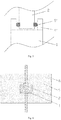

Classifications
-
- H—ELECTRICITY
- H01—ELECTRIC ELEMENTS
- H01J—ELECTRIC DISCHARGE TUBES OR DISCHARGE LAMPS
- H01J37/00—Discharge tubes with provision for introducing objects or material to be exposed to the discharge, e.g. for the purpose of examination or processing thereof
- H01J37/32—Gas-filled discharge tubes
- H01J37/32431—Constructional details of the reactor
- H01J37/32715—Workpiece holder
-
- C—CHEMISTRY; METALLURGY
- C23—COATING METALLIC MATERIAL; COATING MATERIAL WITH METALLIC MATERIAL; CHEMICAL SURFACE TREATMENT; DIFFUSION TREATMENT OF METALLIC MATERIAL; COATING BY VACUUM EVAPORATION, BY SPUTTERING, BY ION IMPLANTATION OR BY CHEMICAL VAPOUR DEPOSITION, IN GENERAL; INHIBITING CORROSION OF METALLIC MATERIAL OR INCRUSTATION IN GENERAL
- C23C—COATING METALLIC MATERIAL; COATING MATERIAL WITH METALLIC MATERIAL; SURFACE TREATMENT OF METALLIC MATERIAL BY DIFFUSION INTO THE SURFACE, BY CHEMICAL CONVERSION OR SUBSTITUTION; COATING BY VACUUM EVAPORATION, BY SPUTTERING, BY ION IMPLANTATION OR BY CHEMICAL VAPOUR DEPOSITION, IN GENERAL
- C23C14/00—Coating by vacuum evaporation, by sputtering or by ion implantation of the coating forming material
- C23C14/22—Coating by vacuum evaporation, by sputtering or by ion implantation of the coating forming material characterised by the process of coating
- C23C14/50—Substrate holders
- C23C14/505—Substrate holders for rotation of the substrates
-
- H—ELECTRICITY
- H01—ELECTRIC ELEMENTS
- H01J—ELECTRIC DISCHARGE TUBES OR DISCHARGE LAMPS
- H01J37/00—Discharge tubes with provision for introducing objects or material to be exposed to the discharge, e.g. for the purpose of examination or processing thereof
- H01J37/32—Gas-filled discharge tubes
- H01J37/32009—Arrangements for generation of plasma specially adapted for examination or treatment of objects, e.g. plasma sources
- H01J37/32082—Radio frequency generated discharge
- H01J37/32174—Circuits specially adapted for controlling the RF discharge
-
- H—ELECTRICITY
- H01—ELECTRIC ELEMENTS
- H01J—ELECTRIC DISCHARGE TUBES OR DISCHARGE LAMPS
- H01J37/00—Discharge tubes with provision for introducing objects or material to be exposed to the discharge, e.g. for the purpose of examination or processing thereof
- H01J37/32—Gas-filled discharge tubes
- H01J37/32431—Constructional details of the reactor
- H01J37/32532—Electrodes
- H01J37/32568—Relative arrangement or disposition of electrodes; moving means
-
- H—ELECTRICITY
- H01—ELECTRIC ELEMENTS
- H01J—ELECTRIC DISCHARGE TUBES OR DISCHARGE LAMPS
- H01J37/00—Discharge tubes with provision for introducing objects or material to be exposed to the discharge, e.g. for the purpose of examination or processing thereof
- H01J37/32—Gas-filled discharge tubes
- H01J37/32431—Constructional details of the reactor
- H01J37/32532—Electrodes
- H01J37/32577—Electrical connecting means
-
- H—ELECTRICITY
- H01—ELECTRIC ELEMENTS
- H01J—ELECTRIC DISCHARGE TUBES OR DISCHARGE LAMPS
- H01J37/00—Discharge tubes with provision for introducing objects or material to be exposed to the discharge, e.g. for the purpose of examination or processing thereof
- H01J37/32—Gas-filled discharge tubes
- H01J37/34—Gas-filled discharge tubes operating with cathodic sputtering
- H01J37/3411—Constructional aspects of the reactor
- H01J37/3435—Target holders (includes backing plates and endblocks)
-
- H—ELECTRICITY
- H01—ELECTRIC ELEMENTS
- H01J—ELECTRIC DISCHARGE TUBES OR DISCHARGE LAMPS
- H01J37/00—Discharge tubes with provision for introducing objects or material to be exposed to the discharge, e.g. for the purpose of examination or processing thereof
- H01J37/32—Gas-filled discharge tubes
- H01J37/34—Gas-filled discharge tubes operating with cathodic sputtering
- H01J37/3411—Constructional aspects of the reactor
- H01J37/3444—Associated circuits
-
- H—ELECTRICITY
- H10—SEMICONDUCTOR DEVICES; ELECTRIC SOLID-STATE DEVICES NOT OTHERWISE PROVIDED FOR
- H10P—GENERIC PROCESSES OR APPARATUS FOR THE MANUFACTURE OR TREATMENT OF DEVICES COVERED BY CLASS H10
- H10P72/00—Handling or holding of wafers, substrates or devices during manufacture or treatment thereof
- H10P72/70—Handling or holding of wafers, substrates or devices during manufacture or treatment thereof for supporting or gripping
- H10P72/76—Handling or holding of wafers, substrates or devices during manufacture or treatment thereof for supporting or gripping using mechanical means, e.g. clamps or pinches
- H10P72/7604—Handling or holding of wafers, substrates or devices during manufacture or treatment thereof for supporting or gripping using mechanical means, e.g. clamps or pinches the wafers being placed on a susceptor, stage or support
- H10P72/7618—Handling or holding of wafers, substrates or devices during manufacture or treatment thereof for supporting or gripping using mechanical means, e.g. clamps or pinches the wafers being placed on a susceptor, stage or support characterised by a movable susceptor, stage or support, others than those only rotating on their own vertical axis, e.g. susceptors on a rotating carrousel
-
- H—ELECTRICITY
- H10—SEMICONDUCTOR DEVICES; ELECTRIC SOLID-STATE DEVICES NOT OTHERWISE PROVIDED FOR
- H10P—GENERIC PROCESSES OR APPARATUS FOR THE MANUFACTURE OR TREATMENT OF DEVICES COVERED BY CLASS H10
- H10P95/00—Generic processes or apparatus for manufacture or treatments not covered by the other groups of this subclass
Definitions
- the present disclosure relates to the field of semiconductor manufacturing technology, and in particular, to a power feeding mechanism, a rotary base device, and semiconductor processing equipment.
- the power output from a sputtering power supply is coupled to a processing chamber through an electrode to excite a process gas in the chamber to form plasma, and thin film deposition is achieved under the action of electrons and ions in the plasma.
- PVD physical vapor deposition
- the uniformity of the deposited thin film can be significantly improved by using a rotating base, which has been widely used.
- a radio frequency is generally fed into a base to increase the energy of charged ions in the plasma and enhance the bombardment effect of the ions, but it is a challenge to maintain good and stable radio frequency connection during the rotation of the base.
- the power transmission efficiency is low due to magnetic flux leakage occurring when the radio frequency power is transmitted by means of inductive coupling through the inductance coils.
- the present disclosure provides a power feeding mechanism, a rotary base device, and semiconductor processing equipment, which can not only improve the power transmission efficiency, but also avoid the risk of ignition in the prior art.
- a power feeding mechanism for feeding output power of a power source into a rotating component, and including:
- the conductive rotating member is disposed opposite to and spaced apart from the conductive stationary member and the conductive connecting structure is disposed in a gap between the conductive rotating member and the conductive stationary member.
- a vertical length of the gap is greater than or equal to 1mm.
- a surface of the conductive rotating member and a surface of the conductive stationary member that are opposite to each other are parallel to each other or are embedded in each other.
- the conductive connecting structure includes a first elastic conductive member.
- the first elastic conductive member is a ring body, a planar spiral body or a columnar spiral body.
- the first elastic conductive member is made of a soft alloy.
- a mounting groove is provided on at least one of a surface of the conductive rotating member and a surface of the conductive stationary member that are opposite to each other, and a part of the first elastic conductive member is disposed in the mounting groove.
- the conductive connecting structure includes a second elastic conductive member, a third elastic conductive member and a spring, wherein two ends of the spring are connected to the conductive stationary member and the second elastic conductive member thereabove, respectively; the third elastic conductive member is provided on the second elastic conductive member and is kept in electrical contact with the conductive rotating member under action of elastic force of the spring; and a hardness of the second elastic conductive member is lower than that of the third elastic conductive member.
- the conductive rotating member is provided with a recess, and at least a part of the second elastic conductive member is located in the recess.
- the conductive connecting structure further includes a fixing seat connected to the spring; and a mounting groove is provided on the fixing seat, and the second elastic conductive member is detachably fixed in the mounting groove.
- the conductive connecting structure includes:
- the second elastic conductive member is made of graphite or a soft alloy.
- the third elastic conductive member is a ring body, a planar spiral body or a columnar spiral body.
- the third elastic conductive member is made of a soft alloy.
- the power feeding mechanism further includes a conductive liquid container, and a part of the conductive stationary member and a part of the conductive rotating member are immersed in a conductive liquid in the conductive liquid container, so as to electrically connect the conductive stationary member to the conductive rotating member through the conductive liquid.
- the conductive liquid container is connected to the conductive stationary member or the conductive rotating member.
- the conductive connecting structure further includes a conductive liquid container, and a part of the conductive stationary member and a part of the conductive rotating member are immersed in a conductive liquid in the conductive liquid container, so as to electrically connect the conductive stationary member to the conductive rotating member through the conductive liquid.
- the rotating component includes a base, a target or a coil.
- the present disclosure further provides a rotary base device, including a rotatable base, a bias power source, and a power feeding mechanism, the power feeding mechanism is used to feed output power of the bias power source into the base, and is the above power feeding mechanism provided by the present disclosure.
- the rotary base device further includes:
- the present disclosure further provides semiconductor processing equipment, including a reaction chamber, and the above rotary base device provided by the present disclosure, the rotary base device being disposed in the reaction chamber.
- the present disclosure has the following beneficial effects: in the power feeding mechanism, the rotary base device and the semiconductor processing equipment of the present disclosure, the conductive connecting structure is in electrical contact respectively with the conductive stationary member and the conductive rotating member without affecting the rotation of the conductive rotating member, so that the power can be transmitted to the rotating component that is rotating. Meanwhile, because the conductive connecting structure is in electrical contact respectively with the conductive stationary member and the conductive rotating member, the power transmission efficiency is higher and the risk of ignition in the prior art can be avoided as compared with transmitting the power by means of inductive coupling in the prior art.
- the power feeding mechanism is used for feeding output power of a power source into a rotating component.
- the rotating component may be a base, a target, a coil, etc.
- the power source usually includes a matcher and a power supply.
- the matcher is used to dynamically adjust a variable capacitor in a matching circuit in a processing process to make load impedance be matched with output impedance of the power supply, so as to ensure that the output power of the power supply is applied to the plasma inside a chamber to the greatest extent.
- the power supply includes a radio frequency power supply, a low frequency power supply, an intermediate frequency power supply, a direct current power supply, or the like.
- the power feeding mechanism includes: a conductive stationary member, a conductive rotating member and a conductive connecting structure.
- the conductive stationary member is electrically connected with the power source; the conductive rotating member is electrically connected and synchronously rotates with the rotating component; and the conductive connecting structure is in electrical contact with the conductive stationary member and the conductive rotating member, respectively, without affecting the rotation of the conductive rotating member.
- the output power of the power source can be fed into the rotating component that is rotating.
- the conductive connecting structure is in electrical contact with the conductive stationary member and the conductive rotating member, respectively, the power transmission efficiency is higher and the risk of ignition in the prior art can be avoided as compared with transmitting the power by means of inductive coupling in the prior art.
- a conductive rotating member 2 is disposed opposite to and spaced apart from a conductive stationary member 1.
- a conductive connecting structure is provided in a gap between the conductive rotating member 2 and the conductive stationary member 1 to electrically connect the conductive rotating member 2 to the conductive stationary member 1, thereby achieving power transmission.
- the conductive rotating member 2 includes a first surface 21, the conductive stationary member 1 includes a second surface 11, and the first surface 21 is opposite to and spaced apart from the second surface 11.
- a vertical length of the gap between the conductive rotating member 2 and the conductive stationary member 1 is greater than or equal to 1mm, that is, there is a distance D between the first surface 21 and the second surface 11, and D is greater than or equal to 1mm. In this way, it can be ensured that the rotation of the conductive rotating member 2 is not affected.
- the conductive stationary member 1 and the conductive rotating member 2 are preferably made of a material having good conductivity, such as copper.
- the two opposite surfaces (the first surface 21 and the second surface 11) of the conductive rotating member 2 and the conductive stationary member 1 are parallel to each other or are embedded in each other, so as to improve structural stability.
- a concave portion 211 is provided on the first surface 21, and a convex portion 111 is correspondingly provided on the second surface 11; and the convex portion 111 is located in the concave portion 211, so that the conductive rotating member 2 and the conductive stationary member 1 are embedded in each other.
- the convex portion may be provided on the first surface 21, and the concave portion may be correspondingly provided on the second surface 11.
- the conductive connecting structure includes a first elastic conductive member 3. Due to its elasticity, the first elastic conductive member 3 can always be kept in electrical contact with the conductive rotating member 2 during the rotation of the conductive rotating member 2, so as to ensure normal power transmission. Meanwhile, the first elastic conductive member 3 does not affect the rotation of the conductive rotating member.
- the first elastic conductive member 3 may be made of a soft material, for example, a soft alloy such as an aluminum alloy and a stainless steel alloy.
- the first elastic conductive member 3 is located between a bottom surface of the concave portion 211 and a top surface of the convex portion 111 in the embodiment, but the present disclosure is not limited thereto. In practical applications, as shown in Fig. 2 , the first elastic conductive member 3 may be located between an inner wall surface of the concave portion 211 and an outer wall surface of the convex portion 111.
- both a first surface 21' and a second surface 11' are flat surfaces, and the first elastic conductive member 3 is disposed between the first surface 21' and the second surface 11'.
- the first elastic conductive member 3 is a ring body.
- the first elastic conductive member 3 may be any other structure such as a planar spiral body (like a spiral body of an incense coil) or a columnar spiral body.
- a mounting groove 22 is provided on the first surface 21, and part of the first elastic conductive member 3 is disposed in the mounting groove 22 to mount the first elastic conductive member 3. It is easily understood that the other part of the first elastic conductive member 3 is located outside the mounting groove 22 to guarantee the electrical contact with the second surface 11 of the conductive stationary member 1.
- the mounting groove may be provided on the second surface 11, or it is also possible to arrange corresponding mounting grooves respectively on the first surface 21 and the second surface 11.
- first elastic conductive member 3 in the embodiment is one, but the present disclosure is not limited thereto. In practical applications, a plurality of annular first elastic conductive members 3 may be provided and embedded in each other. For the first elastic conductive members 3 having other structures, any other arrangement may be applicable.
- the power feeding mechanism provided in a second embodiment of the present disclosure also includes a conductive stationary member, a conductive rotating member and a conductive connecting structure, but the conductive connecting structure has a different structure. Only the differences between the second embodiment and the first embodiment are described below.
- the conductive connecting structure includes: a spring 7, a second elastic conductive member 4, and a third elastic conductive member 5.
- a first end of the spring 7 (a lower end of the spring 7 in Fig. 4 ) is connected to the conductive stationary member 1, and a second end of the spring 7 (an upper end of the spring 7 in Fig. 4 ) is connected to the second elastic conductive member 4.
- the third elastic conductive member 5 is disposed on the second elastic conductive member 4, and is kept in electrical contact with the conductive rotating member 2 under the action of the elastic force of the spring 7.
- the hardness of the second elastic conductive member 4 is lower than that of the third elastic conductive member 5.
- the conductive rotating member 2 drives the third elastic conductive member 5 to rotate together, which causes relative movement between the third elastic conductive member 5 and the second elastic conductive member 4. Since the hardness of the second elastic conductive member 4 is lower than that of the third elastic conductive member 5, the second elastic conductive member 4, which is softer, is more likely to be worn by the third elastic conductive member 5, so that the wear of the third elastic conductive member 5 is reduced and the service life of the third elastic conductive member 5 is prolonged.
- the electrical contact between the third elastic conductive member 5 and the conductive rotating member 2 can still be kept in good condition under the action of the elastic force of the spring 7, thereby ensuring stable power transmission.
- the second elastic conductive member 4 may be made of a soft material such as graphite or a soft alloy.
- the third elastic conductive member 5 may be made of a soft material such as a soft alloy.
- the graphite powder generated by graphite during operation can lubricate the third elastic conductive member 5, so as to further reduce the wear of the third elastic conductive member 5.
- the third elastic conductive member 5 may be a ring body, a planar spiral body, a columnar spiral body, or the like.
- the spring 7 may be an elastic member such as a cylindrical coil spring.
- the conductive rotating member 2 is provided with a recess 23, and at least a part of the second elastic conductive member 4 is located in the recess 23, so that the conductive rotating member 2 and the second elastic conductive member 4 can be embedded in each other to improve structural stability.
- the conductive connecting structure further includes a fixing seat 6 connected to the spring 7; and a mounting groove is provided on the fixing seat 6, and the second elastic conductive member 4 is detachably fixed in the mounting groove.
- the second elastic conductive member 4 can be separated from the conductive rotating member 2 by pressing the fixing seat 6 downward, then taken away from the mounting groove, and replaced with a new second elastic conductive member 4, which is easier than replacing the third elastic conductive member 5, thereby increasing work efficiency.
- the power feeding mechanism provided in a third embodiment of the present disclosure also includes a conductive stationary member, a conductive rotating member and a conductive connecting structure, but the conductive connecting structure has a different structure. Only the differences between the third embodiment and the second embodiment are described below.
- the conductive connecting structure includes: a second elastic conductive member 4' and a third elastic conductive member 5', and the second elastic conductive member 4' is connected with the conductive stationary member 1 and is a ring body that is disposed around the conductive rotating member 2.
- the third elastic conductive member 5' is connected with the conductive rotating member 2, located between an inner wall surface of the ring body and an outer wall surface of the conductive rotating member 2, and in electrical contact with the ring body and the conductive rotating member 2 respectively.
- the hardness of the second elastic conductive member 4' is lower than that of the third elastic conductive member 5'.
- the third elastic conductive member 5' synchronously rotates with the conductive rotating member 2, which causes relative movement between the third elastic conductive member 5'and the second elastic conductive member 4'. Since the hardness of the second elastic conductive member 4' is lower than that of the third elastic conductive member 5', the second elastic conductive member 4', which is softer, is more likely to be worn by the third elastic conductive member 5', so that the wear of the third elastic conductive member 5' is reduced and the service life of the third elastic conductive member 5' is prolonged.
- the power feeding mechanism provided in a fourth embodiment of the present disclosure is obtained by making an improvement to the power feeding mechanisms provided by the above embodiments.
- a conductive connecting structure includes a conductive liquid container 8 filled with a conductive liquid 9, and a part of the conductive stationary member 1 and a part of the conductive rotating member 2 are immersed in the conductive liquid 9 in the conductive liquid container 8, so as to electrically connect the conductive stationary member 1 to the conductive rotating member 2 through the conductive liquid.
- the conductive liquid has stable conductivity because it does not settle or agglomerate even being used for a long time.
- the conductive liquid may be mercury, a conductive carbon-based solvent, a conductive ionic solution, or any other conductive liquid.
- the conductive liquid container 8 may be connected to the conductive stationary member 1, and in this case, the conductive liquid container 8 is fixed relative to the conductive rotating member 2 that is rotating; or, the conductive liquid container 8 may be connected to the conductive rotating member 2, and in this case, the conductive liquid container 8 synchronously rotates with the conductive rotating member 2.
- the conductive liquid container 8 may be used together with the conductive connecting structures provided in the first to third embodiments. Taking the first embodiment as an example, with reference to Fig. 1 , in addition to the first elastic conductive member 3 disposed between the first surface 21 and the second surface 11, the conductive liquid container 8 may also be provided to fill the gap between the first surface 21 and the second surface 11 with the conductive liquid.
- the conductive connecting structure may be the conductive liquid container 8 alone, that is, only the conductive liquid container 8 is used to electrically connect the conductive stationary member 1 to the conductive rotating member 2.
- the first elastic conductive member 3 in the first embodiment is replaced with the conductive liquid container 8.
- the conductive stationary member 1 and the conductive rotating member 2 are embedded in each other as described in the first embodiment to allow the gap therebetween to be fully filled with the conductive liquid 9, so that the conductive liquid 9 can be uniformly distributed between the conductive stationary member 1 and the conductive rotating member 2.
- the conductive connecting structure can be in electrical contact with the conductive stationary member and the conductive rotating member respectively without affecting the rotation of the conductive rotating member, so that the power may be transmitted to the rotating component that is rotating. Meanwhile, because the conductive connecting structure is in electrical contact with the conductive stationary member and the conductive rotating member respectively, the power transmission efficiency is higher and the risk of ignition in the prior art can be avoided as compared with transmitting the power by means of inductive coupling in the prior art.
- a fifth embodiment of the present disclosure provides a rotary base device, including a base 101 that is rotatable, a target 102, an upper radio frequency power supply 103, a bias power source, and a power feeding mechanism 105.
- the base 101 is disposed in a reaction chamber 100, and is the rotating component in the above embodiments.
- the target 102 is disposed above the base 101 and is electrically connected to the upper radio frequency power supply 103.
- the bias power source includes a matcher 106 and a power supply 107, the matcher 106 is used to dynamically adjust a variable capacitor in a matching circuit during a processing process to make load impedance be matched with the output impedance of the power supply 107, so as to ensure that the output power of the power supply 107 is applied to the plasma inside the chamber to the greatest extent.
- the power supply 107 includes a radio frequency power supply, a low frequency power supply, an intermediate frequency power supply, a direct current power supply, or the like.
- the power feeding mechanism 105 is used to feed the output power of the bias power source into the base 101, and is the power feeding mechanism provided in each of the above embodiments of the present disclosure.
- the rotary base device further includes: a rotating shaft 104 and a rotation driving mechanism 108.
- the rotating shaft 104 is vertically disposed, and has an upper end connected with the base 101 and a lower end connected with the power feeding mechanism 105.
- the rotating shaft 104 is used as the conductive rotating member and is electrically connected with the base 101, and the lower part of the rotating shaft 104 is opposite to and spaced apart from the conductive stationary member.
- the conductive connecting structure is disposed in a gap between the rotating shaft 104 and the conductive stationary member to electrically connect the rotating shaft 104 to the conductive stationary member, thereby achieving power transmission.
- the rotation driving mechanism 108 is connected with a middle part between the upper end and the lower end of the rotating shaft 104, so as to drive the rotating shaft 104 to rotate.
- the rotation driving mechanism 108 may include a motor and a transmission mechanism, and the motor is connected to the rotating shaft 104 through the transmission mechanism.
- the transmission mechanism may be, for example, a belt transmission mechanism, a gear transmission mechanism, etc. It should be noted that the rotation driving mechanism 108 bears the weight of the rotating shaft 104 and the base 101 thereon.
- the rotary base device provided in the embodiment can not only improve the power transmission efficiency, but also avoid the risk of ignition in the prior art.
- the embodiment of the present disclosure further provides semiconductor processing equipment, including the reaction chamber 100, and the rotary base device provided in each of the above embodiments of the present disclosure, the rotary base device being disposed in the reaction chamber 100.
- the semiconductor processing equipment provided in the embodiment can not only improve the power transmission efficiency, but also avoid the risk of ignition in the prior art.
Landscapes
- Chemical & Material Sciences (AREA)
- Engineering & Computer Science (AREA)
- Physics & Mathematics (AREA)
- Plasma & Fusion (AREA)
- Analytical Chemistry (AREA)
- Materials Engineering (AREA)
- Chemical Kinetics & Catalysis (AREA)
- Mechanical Engineering (AREA)
- Metallurgy (AREA)
- Organic Chemistry (AREA)
- Charge And Discharge Circuits For Batteries Or The Like (AREA)
- Physical Or Chemical Processes And Apparatus (AREA)
- Current-Collector Devices For Electrically Propelled Vehicles (AREA)
Abstract
Description
- The present disclosure relates to the field of semiconductor manufacturing technology, and in particular, to a power feeding mechanism, a rotary base device, and semiconductor processing equipment.
- In a physical vapor deposition (PVD) process, the power output from a sputtering power supply is coupled to a processing chamber through an electrode to excite a process gas in the chamber to form plasma, and thin film deposition is achieved under the action of electrons and ions in the plasma.
- With the increase of wafer size, there are higher and higher requirements for the uniformity of a deposited thin film in the PVD process in order to improve the yield of products. The uniformity of the deposited thin film can be significantly improved by using a rotating base, which has been widely used. A radio frequency is generally fed into a base to increase the energy of charged ions in the plasma and enhance the bombardment effect of the ions, but it is a challenge to maintain good and stable radio frequency connection during the rotation of the base.
- In the prior art, generally, two mutually embedded inductance coils are disposed around a rotatable base supporting member; by using a magnetic field generated by the inductance coils, radio frequency energy can be coupled to the base supporting member by means of magnetic field coupling, so as to transmit radio frequency power to the base that is rotating. However, following problems are inevitable in practical applications.
- Firstly, the power transmission efficiency is low due to magnetic flux leakage occurring when the radio frequency power is transmitted by means of inductive coupling through the inductance coils.
- Secondly, in order to increase the radio frequency power that is fed into the base supporting member, a voltage of the inductance coils needs to be increased, but there is a risk of ignition when the voltage is increased to a certain threshold.
- In order to solve at least one of the problems in the prior art, the present disclosure provides a power feeding mechanism, a rotary base device, and semiconductor processing equipment, which can not only improve the power transmission efficiency, but also avoid the risk of ignition in the prior art.
- To achieve the objective of the present disclosure, there is provided a power feeding mechanism for feeding output power of a power source into a rotating component, and including:
- a conductive stationary member, which is electrically connected with the power source;
- a conductive rotating member, which is electrically connected with the rotating component and synchronously rotates with the rotating component; and
- a conductive connecting structure, which is in electrical contact with the conductive stationary member and the conductive rotating member, respectively, without affecting rotation of the conductive rotating member.
- Optionally, the conductive rotating member is disposed opposite to and spaced apart from the conductive stationary member and the conductive connecting structure is disposed in a gap between the conductive rotating member and the conductive stationary member.
- Optionally, a vertical length of the gap is greater than or equal to 1mm.
- Optionally, a surface of the conductive rotating member and a surface of the conductive stationary member that are opposite to each other are parallel to each other or are embedded in each other.
- Optionally, the conductive connecting structure includes a first elastic conductive member.
- Optionally, the first elastic conductive member is a ring body, a planar spiral body or a columnar spiral body.
- Optionally, the first elastic conductive member is made of a soft alloy.
- Optionally, a mounting groove is provided on at least one of a surface of the conductive rotating member and a surface of the conductive stationary member that are opposite to each other, and a part of the first elastic conductive member is disposed in the mounting groove.
- Optionally, the conductive connecting structure includes a second elastic conductive member, a third elastic conductive member and a spring, wherein
two ends of the spring are connected to the conductive stationary member and the second elastic conductive member thereabove, respectively;
the third elastic conductive member is provided on the second elastic conductive member and is kept in electrical contact with the conductive rotating member under action of elastic force of the spring; and
a hardness of the second elastic conductive member is lower than that of the third elastic conductive member. - Optionally, the conductive rotating member is provided with a recess, and at least a part of the second elastic conductive member is located in the recess.
- Optionally, the conductive connecting structure further includes a fixing seat connected to the spring; and
a mounting groove is provided on the fixing seat, and the second elastic conductive member is detachably fixed in the mounting groove. - Optionally, the conductive connecting structure includes:
- a second elastic conductive member, which is connected with the conductive stationary member and is a ring body disposed around the conductive rotating member;
- a third elastic conductive member, which is connected with the conductive rotating member, is located between an inner wall surface of the ring body and an outer wall surface of the conductive rotating member, and is in electrical contact with the ring body and the conductive rotating member respectively; and
- a hardness of the second elastic conductive member is lower than that of the third elastic conductive member.
- Optionally, the second elastic conductive member is made of graphite or a soft alloy.
- Optionally, the third elastic conductive member is a ring body, a planar spiral body or a columnar spiral body.
- Optionally, the third elastic conductive member is made of a soft alloy.
- Optionally, the power feeding mechanism further includes a conductive liquid container, and a part of the conductive stationary member and a part of the conductive rotating member are immersed in a conductive liquid in the conductive liquid container, so as to electrically connect the conductive stationary member to the conductive rotating member through the conductive liquid.
- Optionally, the conductive liquid container is connected to the conductive stationary member or the conductive rotating member.
- Optionally, the conductive connecting structure further includes a conductive liquid container, and a part of the conductive stationary member and a part of the conductive rotating member are immersed in a conductive liquid in the conductive liquid container, so as to electrically connect the conductive stationary member to the conductive rotating member through the conductive liquid.
- Optionally, the rotating component includes a base, a target or a coil.
- As another technical solution, the present disclosure further provides a rotary base device, including a rotatable base, a bias power source, and a power feeding mechanism, the power feeding mechanism is used to feed output power of the bias power source into the base, and is the above power feeding mechanism provided by the present disclosure.
- Optionally, the rotary base device further includes:
- a rotating shaft, which is vertically disposed, and has an upper end connected with the base and a lower end connected with the power feeding mechanism; and
- a rotation driving mechanism, which is connected with a middle part between the upper end and the lower end of the rotating shaft, so as to drive the rotating shaft to rotate.
- As another technical solution, the present disclosure further provides semiconductor processing equipment, including a reaction chamber, and the above rotary base device provided by the present disclosure, the rotary base device being disposed in the reaction chamber.
- The present disclosure has the following beneficial effects:
in the power feeding mechanism, the rotary base device and the semiconductor processing equipment of the present disclosure, the conductive connecting structure is in electrical contact respectively with the conductive stationary member and the conductive rotating member without affecting the rotation of the conductive rotating member, so that the power can be transmitted to the rotating component that is rotating. Meanwhile, because the conductive connecting structure is in electrical contact respectively with the conductive stationary member and the conductive rotating member, the power transmission efficiency is higher and the risk of ignition in the prior art can be avoided as compared with transmitting the power by means of inductive coupling in the prior art. -
-
Fig. 1 is a structural diagram of a power feeding mechanism according to a first embodiment of the present disclosure; -
Fig. 2 is another structural diagram of the power feeding mechanism according to the first embodiment of the present disclosure; -
Fig. 3 is still another structural diagram of the power feeding mechanism according to the first embodiment of the present disclosure; -
Fig. 4 is a structural diagram of a power feeding mechanism according to a second embodiment of the present disclosure; -
Fig. 5 is a structural diagram of a power feeding mechanism according to a third embodiment of the present disclosure; -
Fig. 6 is a structural diagram of a power feeding mechanism according to a fourth embodiment of the present disclosure; and -
Fig. 7 is a structural diagram of semiconductor processing equipment according to a fifth embodiment of the present disclosure. - In order to enable those skilled in the art to better understand the technical solutions of the present disclosure, the power feeding mechanism, the rotary base device and the semiconductor processing equipment provided by the present disclosure are described in detail below with reference to the accompanying drawings.
- The power feeding mechanism provided by the present disclosure is used for feeding output power of a power source into a rotating component. The rotating component may be a base, a target, a coil, etc. The power source usually includes a matcher and a power supply. The matcher is used to dynamically adjust a variable capacitor in a matching circuit in a processing process to make load impedance be matched with output impedance of the power supply, so as to ensure that the output power of the power supply is applied to the plasma inside a chamber to the greatest extent. The power supply includes a radio frequency power supply, a low frequency power supply, an intermediate frequency power supply, a direct current power supply, or the like.
- Specifically, the power feeding mechanism includes: a conductive stationary member, a conductive rotating member and a conductive connecting structure. The conductive stationary member is electrically connected with the power source; the conductive rotating member is electrically connected and synchronously rotates with the rotating component; and the conductive connecting structure is in electrical contact with the conductive stationary member and the conductive rotating member, respectively, without affecting the rotation of the conductive rotating member. In this way, the output power of the power source can be fed into the rotating component that is rotating. Meanwhile, because the conductive connecting structure is in electrical contact with the conductive stationary member and the conductive rotating member, respectively, the power transmission efficiency is higher and the risk of ignition in the prior art can be avoided as compared with transmitting the power by means of inductive coupling in the prior art.
- The specific implementations of the conductive connecting structure are described in detail below. Specifically, with reference to
Fig. 1 , in the power feeding mechanism according to a first embodiment of the present disclosure, a conductive rotatingmember 2 is disposed opposite to and spaced apart from a conductivestationary member 1. A conductive connecting structure is provided in a gap between the conductive rotatingmember 2 and the conductivestationary member 1 to electrically connect the conductive rotatingmember 2 to the conductivestationary member 1, thereby achieving power transmission. - In the embodiment, the conductive rotating
member 2 includes afirst surface 21, the conductivestationary member 1 includes asecond surface 11, and thefirst surface 21 is opposite to and spaced apart from thesecond surface 11. Preferably, a vertical length of the gap between the conductive rotatingmember 2 and the conductivestationary member 1 is greater than or equal to 1mm, that is, there is a distance D between thefirst surface 21 and thesecond surface 11, and D is greater than or equal to 1mm. In this way, it can be ensured that the rotation of the conductive rotatingmember 2 is not affected. The conductivestationary member 1 and the conductive rotatingmember 2 are preferably made of a material having good conductivity, such as copper. - In the embodiment, the two opposite surfaces (the
first surface 21 and the second surface 11) of the conductive rotatingmember 2 and the conductivestationary member 1 are parallel to each other or are embedded in each other, so as to improve structural stability. In the embodiment, aconcave portion 211 is provided on thefirst surface 21, and aconvex portion 111 is correspondingly provided on thesecond surface 11; and theconvex portion 111 is located in theconcave portion 211, so that the conductive rotatingmember 2 and the conductivestationary member 1 are embedded in each other. In practical applications, the convex portion may be provided on thefirst surface 21, and the concave portion may be correspondingly provided on thesecond surface 11. - In the embodiment, the conductive connecting structure includes a first elastic
conductive member 3. Due to its elasticity, the first elasticconductive member 3 can always be kept in electrical contact with the conductive rotatingmember 2 during the rotation of the conductive rotatingmember 2, so as to ensure normal power transmission. Meanwhile, the first elasticconductive member 3 does not affect the rotation of the conductive rotating member. The first elasticconductive member 3 may be made of a soft material, for example, a soft alloy such as an aluminum alloy and a stainless steel alloy. - It should be noted that the first elastic
conductive member 3 is located between a bottom surface of theconcave portion 211 and a top surface of theconvex portion 111 in the embodiment, but the present disclosure is not limited thereto. In practical applications, as shown inFig. 2 , the first elasticconductive member 3 may be located between an inner wall surface of theconcave portion 211 and an outer wall surface of theconvex portion 111. - It should be noted that the conductive rotating
member 2 and the conductivestationary member 1 are embedded in each other through theconcave portion 211 and theconvex portion 111 in the embodiment, but the present disclosure is not limited thereto. In practical applications, as shown inFig. 3 , both a first surface 21' and a second surface 11' are flat surfaces, and the first elasticconductive member 3 is disposed between the first surface 21' and the second surface 11'. - In the embodiment, the first elastic
conductive member 3 is a ring body. In practical applications, the first elasticconductive member 3 may be any other structure such as a planar spiral body (like a spiral body of an incense coil) or a columnar spiral body. - In the embodiment, a mounting
groove 22 is provided on thefirst surface 21, and part of the first elasticconductive member 3 is disposed in the mountinggroove 22 to mount the first elasticconductive member 3. It is easily understood that the other part of the first elasticconductive member 3 is located outside the mountinggroove 22 to guarantee the electrical contact with thesecond surface 11 of the conductivestationary member 1. In practical applications, the mounting groove may be provided on thesecond surface 11, or it is also possible to arrange corresponding mounting grooves respectively on thefirst surface 21 and thesecond surface 11. - It should be noted that the number of the first elastic
conductive member 3 in the embodiment is one, but the present disclosure is not limited thereto. In practical applications, a plurality of annular first elasticconductive members 3 may be provided and embedded in each other. For the first elasticconductive members 3 having other structures, any other arrangement may be applicable. - Compared with the power feeding mechanism provided in the first embodiment, the power feeding mechanism provided in a second embodiment of the present disclosure also includes a conductive stationary member, a conductive rotating member and a conductive connecting structure, but the conductive connecting structure has a different structure. Only the differences between the second embodiment and the first embodiment are described below.
- Specifically, with reference to
Fig. 4 , the conductive connecting structure includes: aspring 7, a second elasticconductive member 4, and a third elasticconductive member 5. A first end of the spring 7 (a lower end of thespring 7 inFig. 4 ) is connected to the conductivestationary member 1, and a second end of the spring 7 (an upper end of thespring 7 inFig. 4 ) is connected to the second elasticconductive member 4. The third elasticconductive member 5 is disposed on the second elasticconductive member 4, and is kept in electrical contact with the conductive rotatingmember 2 under the action of the elastic force of thespring 7. - The hardness of the second elastic
conductive member 4 is lower than that of the third elasticconductive member 5. In practical applications, the conductive rotatingmember 2 drives the third elasticconductive member 5 to rotate together, which causes relative movement between the third elasticconductive member 5 and the second elasticconductive member 4. Since the hardness of the second elasticconductive member 4 is lower than that of the third elasticconductive member 5, the second elasticconductive member 4, which is softer, is more likely to be worn by the third elasticconductive member 5, so that the wear of the third elasticconductive member 5 is reduced and the service life of the third elasticconductive member 5 is prolonged. - Meanwhile, even if the second elastic
conductive member 4 is worn thin, the electrical contact between the third elasticconductive member 5 and the conductive rotatingmember 2 can still be kept in good condition under the action of the elastic force of thespring 7, thereby ensuring stable power transmission. - In practical applications, under the condition that the hardness of the second elastic
conductive member 4 is lower than that of the third elasticconductive member 5, the second elasticconductive member 4 may be made of a soft material such as graphite or a soft alloy. The third elasticconductive member 5 may be made of a soft material such as a soft alloy. The graphite powder generated by graphite during operation can lubricate the third elasticconductive member 5, so as to further reduce the wear of the third elasticconductive member 5. - Like the first elastic
conductive member 3 in the first embodiment, the third elasticconductive member 5 may be a ring body, a planar spiral body, a columnar spiral body, or the like. - Optionally, the
spring 7 may be an elastic member such as a cylindrical coil spring. - In the embodiment, the conductive rotating
member 2 is provided with arecess 23, and at least a part of the second elasticconductive member 4 is located in therecess 23, so that the conductive rotatingmember 2 and the second elasticconductive member 4 can be embedded in each other to improve structural stability. - Optionally, the conductive connecting structure further includes a fixing
seat 6 connected to thespring 7; and a mounting groove is provided on the fixingseat 6, and the second elasticconductive member 4 is detachably fixed in the mounting groove. In this way, after the second elasticconductive member 4 is worn to a certain extent, the second elasticconductive member 4 can be separated from the conductive rotatingmember 2 by pressing the fixingseat 6 downward, then taken away from the mounting groove, and replaced with a new second elasticconductive member 4, which is easier than replacing the third elasticconductive member 5, thereby increasing work efficiency. - Compared with the power feeding mechanism provided in the second embodiment, the power feeding mechanism provided in a third embodiment of the present disclosure also includes a conductive stationary member, a conductive rotating member and a conductive connecting structure, but the conductive connecting structure has a different structure. Only the differences between the third embodiment and the second embodiment are described below.
- Specifically, with reference to
Fig. 5 , the conductive connecting structure includes: a second elastic conductive member 4' and a third elastic conductive member 5', and the second elastic conductive member 4' is connected with the conductivestationary member 1 and is a ring body that is disposed around the conductive rotatingmember 2. The third elastic conductive member 5' is connected with the conductive rotatingmember 2, located between an inner wall surface of the ring body and an outer wall surface of the conductive rotatingmember 2, and in electrical contact with the ring body and the conductive rotatingmember 2 respectively. The hardness of the second elastic conductive member 4' is lower than that of the third elastic conductive member 5'. - The third elastic conductive member 5' synchronously rotates with the conductive rotating
member 2, which causes relative movement between the third elastic conductive member 5'and the second elastic conductive member 4'. Since the hardness of the second elastic conductive member 4' is lower than that of the third elastic conductive member 5', the second elastic conductive member 4', which is softer, is more likely to be worn by the third elastic conductive member 5', so that the wear of the third elastic conductive member 5' is reduced and the service life of the third elastic conductive member 5' is prolonged. - The power feeding mechanism provided in a fourth embodiment of the present disclosure is obtained by making an improvement to the power feeding mechanisms provided by the above embodiments.
- Specifically, with reference to
Fig. 6 , a conductive connecting structure includes a conductiveliquid container 8 filled with aconductive liquid 9, and a part of the conductivestationary member 1 and a part of the conductive rotatingmember 2 are immersed in theconductive liquid 9 in the conductiveliquid container 8, so as to electrically connect the conductivestationary member 1 to the conductive rotatingmember 2 through the conductive liquid. Besides having good conductivity, the conductive liquid has stable conductivity because it does not settle or agglomerate even being used for a long time. The conductive liquid may be mercury, a conductive carbon-based solvent, a conductive ionic solution, or any other conductive liquid. - In practical applications, the conductive
liquid container 8 may be connected to the conductivestationary member 1, and in this case, the conductiveliquid container 8 is fixed relative to the conductive rotatingmember 2 that is rotating; or, the conductiveliquid container 8 may be connected to the conductive rotatingmember 2, and in this case, the conductiveliquid container 8 synchronously rotates with the conductive rotatingmember 2. - In the embodiment, the conductive
liquid container 8 may be used together with the conductive connecting structures provided in the first to third embodiments. Taking the first embodiment as an example, with reference toFig. 1 , in addition to the first elasticconductive member 3 disposed between thefirst surface 21 and thesecond surface 11, the conductiveliquid container 8 may also be provided to fill the gap between thefirst surface 21 and thesecond surface 11 with the conductive liquid. - However, the present disclosure is not limited to the above. In practical applications, the conductive connecting structure may be the conductive
liquid container 8 alone, that is, only the conductiveliquid container 8 is used to electrically connect the conductivestationary member 1 to the conductive rotatingmember 2. For example, the first elasticconductive member 3 in the first embodiment is replaced with the conductiveliquid container 8. Optionally, the conductivestationary member 1 and the conductive rotatingmember 2 are embedded in each other as described in the first embodiment to allow the gap therebetween to be fully filled with theconductive liquid 9, so that theconductive liquid 9 can be uniformly distributed between the conductivestationary member 1 and the conductive rotatingmember 2. - In summary, in the power feeding mechanism provided in each of the above embodiments of the present disclosure, the conductive connecting structure can be in electrical contact with the conductive stationary member and the conductive rotating member respectively without affecting the rotation of the conductive rotating member, so that the power may be transmitted to the rotating component that is rotating. Meanwhile, because the conductive connecting structure is in electrical contact with the conductive stationary member and the conductive rotating member respectively, the power transmission efficiency is higher and the risk of ignition in the prior art can be avoided as compared with transmitting the power by means of inductive coupling in the prior art.
- As another technical solution, with reference to
Fig. 7 , a fifth embodiment of the present disclosure provides a rotary base device, including a base 101 that is rotatable, atarget 102, an upper radiofrequency power supply 103, a bias power source, and apower feeding mechanism 105. Thebase 101 is disposed in areaction chamber 100, and is the rotating component in the above embodiments. Thetarget 102 is disposed above thebase 101 and is electrically connected to the upper radiofrequency power supply 103. The bias power source includes amatcher 106 and apower supply 107, thematcher 106 is used to dynamically adjust a variable capacitor in a matching circuit during a processing process to make load impedance be matched with the output impedance of thepower supply 107, so as to ensure that the output power of thepower supply 107 is applied to the plasma inside the chamber to the greatest extent. Thepower supply 107 includes a radio frequency power supply, a low frequency power supply, an intermediate frequency power supply, a direct current power supply, or the like. - The
power feeding mechanism 105 is used to feed the output power of the bias power source into thebase 101, and is the power feeding mechanism provided in each of the above embodiments of the present disclosure. - In the embodiment, the rotary base device further includes: a rotating
shaft 104 and arotation driving mechanism 108. Therotating shaft 104 is vertically disposed, and has an upper end connected with thebase 101 and a lower end connected with thepower feeding mechanism 105. Therotating shaft 104 is used as the conductive rotating member and is electrically connected with thebase 101, and the lower part of therotating shaft 104 is opposite to and spaced apart from the conductive stationary member. The conductive connecting structure is disposed in a gap between therotating shaft 104 and the conductive stationary member to electrically connect therotating shaft 104 to the conductive stationary member, thereby achieving power transmission. Therotation driving mechanism 108 is connected with a middle part between the upper end and the lower end of therotating shaft 104, so as to drive therotating shaft 104 to rotate. - The
rotation driving mechanism 108 may include a motor and a transmission mechanism, and the motor is connected to therotating shaft 104 through the transmission mechanism. The transmission mechanism may be, for example, a belt transmission mechanism, a gear transmission mechanism, etc. It should be noted that therotation driving mechanism 108 bears the weight of therotating shaft 104 and the base 101 thereon. - By adopting the power feeding mechanism provided in each of the above embodiments of the present disclosure, the rotary base device provided in the embodiment can not only improve the power transmission efficiency, but also avoid the risk of ignition in the prior art.
- As another technical solution, with reference to
Fig. 7 , the embodiment of the present disclosure further provides semiconductor processing equipment, including thereaction chamber 100, and the rotary base device provided in each of the above embodiments of the present disclosure, the rotary base device being disposed in thereaction chamber 100. - By adopting the power feeding mechanisms provided in the embodiments of the present disclosure, the semiconductor processing equipment provided in the embodiment can not only improve the power transmission efficiency, but also avoid the risk of ignition in the prior art.
- It should be understood that the above embodiments are merely exemplary embodiments adopted to illustrate the principles of the present disclosure, and the present disclosure is not limited thereto. Without departing from the spirit and essence of the present disclosure, various modifications and improvements can be made by those skilled in the art, and should be considered to fall within the scope of the present disclosure.
Claims (22)
- A power feeding mechanism for feeding output power of a power source into a rotating component, comprising:a conductive stationary member, which is electrically connected with the power source;a conductive rotating member, which is electrically connected with the rotating component and synchronously rotates with the rotating component; anda conductive connecting structure, which is in electrical contact with the conductive stationary member and the conductive rotating member, respectively, without affecting rotation of the conductive rotating member.
- The power feeding mechanism of claim 1, wherein the conductive rotating member is disposed opposite to and spaced apart from the conductive stationary member; and the conductive connecting structure is disposed in a gap between the conductive rotating member and the conductive stationary member.
- The power feeding mechanism of claim 2, wherein a vertical length of the gap is greater than or equal to 1mm.
- The power feeding mechanism of claim 2, wherein a surface of the conductive rotating member and a surface of the conductive stationary member that are opposite to each other are parallel to each other or are embedded in each other.
- The power feeding mechanism of claim 2, wherein the conductive connecting structure comprises a first elastic conductive member.
- The power feeding mechanism of claim 5, wherein the first elastic conductive member is a ring body, a planar spiral body or a columnar spiral body.
- The power feeding mechanism of claim 5, wherein the first elastic conductive member is made of a soft alloy.
- The power feeding mechanism of claim 5, wherein a mounting groove is provided on at least one of a surface of the conductive rotating member and a surface of the conductive stationary member that are opposite to each other, and a part of the first elastic conductive member is disposed in the mounting groove.
- The power feeding mechanism of claim 1, wherein the conductive connecting structure comprises a second elastic conductive member, a third elastic conductive member and a spring, wherein,
two ends of the spring are connected to the conductive stationary member and the second elastic conductive member thereabove, respectively;
the third elastic conductive member is provided on the second elastic conductive member and is kept in electrical contact with the conductive rotating member under action of elastic force of the spring; and
a hardness of the second elastic conductive member is lower than that of the third elastic conductive member. - The power feeding mechanism of claim 9, wherein the conductive rotating member is provided with a recess, and at least a part of the second elastic conductive member is located in the recess.
- The power feeding mechanism of claim 9, wherein the conductive connecting structure further comprises a fixing seat connected to the spring; and
a mounting groove is provided on the fixing seat, and the second elastic conductive member is detachably fixed in the mounting groove. - The power feeding mechanism of claim 1, wherein the conductive connecting structure comprises:a second elastic conductive member, which is connected with the conductive stationary member and is a ring body disposed around the conductive rotating member;a third elastic conductive member, which is connected with the conductive rotating member, is located between an inner wall surface of the ring body and an outer wall surface of the conductive rotating member, and is in electrical contact with the ring body and the conductive rotating member respectively; anda hardness of the second elastic conductive member is lower than that of the third elastic conductive member.
- The power feeding mechanism of claim 9 or 12, wherein the second elastic conductive member is made of graphite or a soft alloy.
- The power feeding mechanism of claim 9 or 12, wherein the third elastic conductive member is a ring body, a planar spiral body or a columnar spiral body.
- The power feeding mechanism of claim 9 or 12, wherein the third elastic conductive member is made of a soft alloy.
- The power feeding mechanism of any one of claims 1 to 12, further comprising a conductive liquid container, and a part of the conductive stationary member and a part of the conductive rotating member are immersed in a conductive liquid in the conductive liquid container, so as to electrically connect the conductive stationary member to the conductive rotating member through the conductive liquid.
- The power feeding mechanism of claim 16, wherein the conductive liquid container is connected to the conductive stationary member or the conductive rotating member.
- The power feeding mechanism of claim 1, wherein the conductive connecting structure comprises a conductive liquid container, and a part of the conductive stationary member and a part of the conductive rotating member are immersed in a conductive liquid in the conductive liquid container, so as to electrically connect the conductive stationary member to the conductive rotating member through the conductive liquid.
- The power feeding mechanism of claim 1, wherein the rotating component comprises a base, a target or a coil.
- A rotary base device, comprising a rotatable base, a bias power source, and a power feeding mechanism configured to feed output power of the bias power source into the base, wherein the power feeding mechanism is the power feeding mechanism of any one of claims 1 to 18.
- The rotary base device of claim 20, further comprising:a rotating shaft, which is vertically disposed, and has an upper end connected with the base and a lower end connected with the power feeding mechanism; anda rotation driving mechanism, which is connected with a middle part between the upper end and the lower end of the rotating shaft, so as to drive the rotating shaft to rotate.
- Semiconductor processing equipment, comprising a reaction chamber, wherein the rotary base device of claim 20 or 21 is disposed in the reaction chamber.
Applications Claiming Priority (3)
| Application Number | Priority Date | Filing Date | Title |
|---|---|---|---|
| CN201820370506.5U CN208014650U (en) | 2018-03-19 | 2018-03-19 | RF power fed-in mechanism, rotating basis device and semiconductor processing equipment |
| CN201810224905.5A CN108461387B (en) | 2018-03-19 | 2018-03-19 | Power feed-in mechanism, rotating base device and semiconductor processing equipment |
| PCT/CN2018/117901 WO2019179159A1 (en) | 2018-03-19 | 2018-11-28 | Power feeding mechanism, rotating base apparatus, and semiconductor processing device |
Publications (3)
| Publication Number | Publication Date |
|---|---|
| EP3770947A1 true EP3770947A1 (en) | 2021-01-27 |
| EP3770947A4 EP3770947A4 (en) | 2021-12-22 |
| EP3770947B1 EP3770947B1 (en) | 2023-06-07 |
Family
ID=67988180
Family Applications (1)
| Application Number | Title | Priority Date | Filing Date |
|---|---|---|---|
| EP18910945.7A Active EP3770947B1 (en) | 2018-03-19 | 2018-11-28 | Power feeding mechanism, rotating base apparatus, and semiconductor processing device |
Country Status (4)
| Country | Link |
|---|---|
| EP (1) | EP3770947B1 (en) |
| KR (1) | KR102437306B1 (en) |
| SG (1) | SG11202008819VA (en) |
| WO (1) | WO2019179159A1 (en) |
Cited By (2)
| Publication number | Priority date | Publication date | Assignee | Title |
|---|---|---|---|---|
| WO2026100392A1 (en) * | 2024-11-11 | 2026-05-15 | 国立大学法人 東京大学 | Substrate support and substrate processing device |
| WO2026100746A1 (en) * | 2024-11-11 | 2026-05-15 | 東京エレクトロン株式会社 | Electrostatic chuck device and rotating body |
Families Citing this family (3)
| Publication number | Priority date | Publication date | Assignee | Title |
|---|---|---|---|---|
| CN114787206B (en) | 2020-09-16 | 2024-07-30 | 株式会社Lg化学 | Compound, antibacterial deodorizing composition comprising the same, and method for preparing the same |
| CN112323036B (en) * | 2020-11-03 | 2022-10-21 | 北京北方华创微电子装备有限公司 | Power feed-in mechanism, rotating base device and semiconductor processing equipment |
| KR102975564B1 (en) * | 2024-04-24 | 2026-06-10 | 플람 주식회사 | Multi rotating plasma device having liquid conductor |
Family Cites Families (15)
| Publication number | Priority date | Publication date | Assignee | Title |
|---|---|---|---|---|
| JP3446091B2 (en) * | 1995-09-26 | 2003-09-16 | 株式会社徳力本店 | Current collector ring assembly |
| JP2003092343A (en) * | 2001-09-17 | 2003-03-28 | Dainippon Screen Mfg Co Ltd | Substrate holding mechanism, substrate processing apparatus and substrate processing method using the same |
| JP2004273406A (en) * | 2003-03-07 | 2004-09-30 | Jukai:Kk | Method of current collection without slippage |
| CN102469675A (en) * | 2010-11-05 | 2012-05-23 | 北京北方微电子基地设备工艺研究中心有限责任公司 | Power matching apparatus and semiconductor equipment |
| WO2013088598A1 (en) * | 2011-12-15 | 2013-06-20 | キヤノンアネルバ株式会社 | Substrate holder device and vacuum processing device |
| US9809876B2 (en) * | 2014-01-13 | 2017-11-07 | Centre Luxembourgeois De Recherches Pour Le Verre Et La Ceramique (C.R.V.C.) Sarl | Endblock for rotatable target with electrical connection between collector and rotor at pressure less than atmospheric pressure |
| JP2015180768A (en) * | 2014-03-06 | 2015-10-15 | 株式会社日立国際電気 | Substrate processing apparatus, semiconductor device manufacturing method, and recording medium |
| TWI530584B (en) * | 2015-01-16 | 2016-04-21 | 財團法人工業技術研究院 | Brushless rotray plasma electrode structure and film coating system |
| GB201505528D0 (en) * | 2015-03-31 | 2015-05-13 | Gencoa Ltd | Rotational device-III |
| JP6449091B2 (en) * | 2015-04-20 | 2019-01-09 | 東京エレクトロン株式会社 | Slip ring, support mechanism and plasma processing apparatus |
| US10043636B2 (en) * | 2015-12-10 | 2018-08-07 | Lam Research Corporation | Apparatuses and methods for avoiding electrical breakdown from RF terminal to adjacent non-RF terminal |
| JP6462620B2 (en) * | 2016-03-29 | 2019-01-30 | 東京エレクトロン株式会社 | Substrate processing apparatus and substrate processing method |
| CN108461387B (en) * | 2018-03-19 | 2020-06-19 | 北京北方华创微电子装备有限公司 | Power feed-in mechanism, rotating base device and semiconductor processing equipment |
| CN208014650U (en) * | 2018-03-19 | 2018-10-26 | 北京北方华创微电子装备有限公司 | RF power fed-in mechanism, rotating basis device and semiconductor processing equipment |
| CN108448409A (en) | 2018-04-10 | 2018-08-24 | 周琼 | A kind of power distribution cabinet with shock-absorbing function |
-
2018
- 2018-11-28 SG SG11202008819VA patent/SG11202008819VA/en unknown
- 2018-11-28 EP EP18910945.7A patent/EP3770947B1/en active Active
- 2018-11-28 KR KR1020207025963A patent/KR102437306B1/en active Active
- 2018-11-28 WO PCT/CN2018/117901 patent/WO2019179159A1/en not_active Ceased
Cited By (2)
| Publication number | Priority date | Publication date | Assignee | Title |
|---|---|---|---|---|
| WO2026100392A1 (en) * | 2024-11-11 | 2026-05-15 | 国立大学法人 東京大学 | Substrate support and substrate processing device |
| WO2026100746A1 (en) * | 2024-11-11 | 2026-05-15 | 東京エレクトロン株式会社 | Electrostatic chuck device and rotating body |
Also Published As
| Publication number | Publication date |
|---|---|
| KR20200119287A (en) | 2020-10-19 |
| SG11202008819VA (en) | 2020-10-29 |
| KR102437306B1 (en) | 2022-08-29 |
| EP3770947B1 (en) | 2023-06-07 |
| EP3770947A4 (en) | 2021-12-22 |
| WO2019179159A1 (en) | 2019-09-26 |
Similar Documents
| Publication | Publication Date | Title |
|---|---|---|
| EP3770947B1 (en) | Power feeding mechanism, rotating base apparatus, and semiconductor processing device | |
| KR102500394B1 (en) | Wireless electric field power transfer system, method, transmitter and receiver therefor | |
| CN102822381B (en) | Cylindrical rotating magnetron sputtering cathode device and method of depositing material using radio frequency emissions | |
| JP6238288B2 (en) | Deposition apparatus and method for reducing deposition asymmetry | |
| TWI720373B (en) | Power feeding mechanism, rotating base device and semiconductor processing equipment | |
| CN102918175B (en) | Physical vapor deposition chamber with rotating magnet assembly and centrally fed RF power | |
| CN114695065B (en) | Semiconductor processing equipment | |
| CN105734520A (en) | Process chamber | |
| CN208014650U (en) | RF power fed-in mechanism, rotating basis device and semiconductor processing equipment | |
| US12300443B2 (en) | Capacitance value fast-placing vacuum capacitor | |
| CN115679271A (en) | Semiconductor process chamber | |
| KR20170129940A (en) | Vacuum-suction device and vacuum processing device | |
| KR20150003230A (en) | Substrate support with radio frequency(rf) return path | |
| WO2016180443A1 (en) | Radio frequency (rf) - sputter deposition source, deposition apparatus and method of operating thereof | |
| US20200266038A1 (en) | Dual power feed rotary sputtering cathode | |
| WO2016180444A1 (en) | Radio frequency (rf) - sputter deposition source, connector for retrofitting a sputter deposition source, apparatus and method of operating thereof | |
| CN112323036A (en) | Power feed-in mechanism, rotating base device and semiconductor processing equipment | |
| CN110396664A (en) | Ground loop, chamber and Pvd equipment | |
| KR100855173B1 (en) | Vacuum apparatus and power feeding method equipped with a power supply mechanism | |
| KR101382274B1 (en) | Cylindrical plasma cathode device | |
| CN118737797A (en) | Upper electrode structure and semiconductor process equipment | |
| WO2011155479A1 (en) | Etching apparatus | |
| JP2020204059A (en) | Sputtering device | |
| JP2017503074A5 (en) | ||
| JP2016192345A (en) | cyclotron |
Legal Events
| Date | Code | Title | Description |
|---|---|---|---|
| STAA | Information on the status of an ep patent application or granted ep patent |
Free format text: STATUS: THE INTERNATIONAL PUBLICATION HAS BEEN MADE |
|
| PUAI | Public reference made under article 153(3) epc to a published international application that has entered the european phase |
Free format text: ORIGINAL CODE: 0009012 |
|
| STAA | Information on the status of an ep patent application or granted ep patent |
Free format text: STATUS: REQUEST FOR EXAMINATION WAS MADE |
|
| 17P | Request for examination filed |
Effective date: 20200918 |
|
| AK | Designated contracting states |
Kind code of ref document: A1 Designated state(s): AL AT BE BG CH CY CZ DE DK EE ES FI FR GB GR HR HU IE IS IT LI LT LU LV MC MK MT NL NO PL PT RO RS SE SI SK SM TR |
|
| AX | Request for extension of the european patent |
Extension state: BA ME |
|
| DAV | Request for validation of the european patent (deleted) | ||
| DAX | Request for extension of the european patent (deleted) | ||
| A4 | Supplementary search report drawn up and despatched |
Effective date: 20211119 |
|
| RIC1 | Information provided on ipc code assigned before grant |
Ipc: C23C 14/50 20060101ALI20211115BHEP Ipc: H01J 37/34 20060101ALI20211115BHEP Ipc: H01L 21/02 20060101AFI20211115BHEP |
|
| GRAJ | Information related to disapproval of communication of intention to grant by the applicant or resumption of examination proceedings by the epo deleted |
Free format text: ORIGINAL CODE: EPIDOSDIGR1 |
|
| STAA | Information on the status of an ep patent application or granted ep patent |
Free format text: STATUS: GRANT OF PATENT IS INTENDED |
|
| GRAP | Despatch of communication of intention to grant a patent |
Free format text: ORIGINAL CODE: EPIDOSNIGR1 |
|
| INTG | Intention to grant announced |
Effective date: 20230208 |
|
| GRAS | Grant fee paid |
Free format text: ORIGINAL CODE: EPIDOSNIGR3 |
|
| GRAA | (expected) grant |
Free format text: ORIGINAL CODE: 0009210 |
|
| STAA | Information on the status of an ep patent application or granted ep patent |
Free format text: STATUS: THE PATENT HAS BEEN GRANTED |
|
| AK | Designated contracting states |
Kind code of ref document: B1 Designated state(s): AL AT BE BG CH CY CZ DE DK EE ES FI FR GB GR HR HU IE IS IT LI LT LU LV MC MK MT NL NO PL PT RO RS SE SI SK SM TR |
|
| REG | Reference to a national code |
Ref country code: GB Ref legal event code: FG4D |
|
| REG | Reference to a national code |
Ref country code: CH Ref legal event code: EP Ref country code: AT Ref legal event code: REF Ref document number: 1577525 Country of ref document: AT Kind code of ref document: T Effective date: 20230615 Ref country code: DE Ref legal event code: R096 Ref document number: 602018051677 Country of ref document: DE |
|
| P01 | Opt-out of the competence of the unified patent court (upc) registered |
Effective date: 20230515 |
|
| REG | Reference to a national code |
Ref country code: LT Ref legal event code: MG9D |
|
| REG | Reference to a national code |
Ref country code: NL Ref legal event code: MP Effective date: 20230607 |
|
| PG25 | Lapsed in a contracting state [announced via postgrant information from national office to epo] |
Ref country code: SE Free format text: LAPSE BECAUSE OF FAILURE TO SUBMIT A TRANSLATION OF THE DESCRIPTION OR TO PAY THE FEE WITHIN THE PRESCRIBED TIME-LIMIT Effective date: 20230607 Ref country code: NO Free format text: LAPSE BECAUSE OF FAILURE TO SUBMIT A TRANSLATION OF THE DESCRIPTION OR TO PAY THE FEE WITHIN THE PRESCRIBED TIME-LIMIT Effective date: 20230907 Ref country code: ES Free format text: LAPSE BECAUSE OF FAILURE TO SUBMIT A TRANSLATION OF THE DESCRIPTION OR TO PAY THE FEE WITHIN THE PRESCRIBED TIME-LIMIT Effective date: 20230607 |
|
| REG | Reference to a national code |
Ref country code: AT Ref legal event code: MK05 Ref document number: 1577525 Country of ref document: AT Kind code of ref document: T Effective date: 20230607 |
|
| PG25 | Lapsed in a contracting state [announced via postgrant information from national office to epo] |
Ref country code: RS Free format text: LAPSE BECAUSE OF FAILURE TO SUBMIT A TRANSLATION OF THE DESCRIPTION OR TO PAY THE FEE WITHIN THE PRESCRIBED TIME-LIMIT Effective date: 20230607 Ref country code: NL Free format text: LAPSE BECAUSE OF FAILURE TO SUBMIT A TRANSLATION OF THE DESCRIPTION OR TO PAY THE FEE WITHIN THE PRESCRIBED TIME-LIMIT Effective date: 20230607 Ref country code: LV Free format text: LAPSE BECAUSE OF FAILURE TO SUBMIT A TRANSLATION OF THE DESCRIPTION OR TO PAY THE FEE WITHIN THE PRESCRIBED TIME-LIMIT Effective date: 20230607 Ref country code: LT Free format text: LAPSE BECAUSE OF FAILURE TO SUBMIT A TRANSLATION OF THE DESCRIPTION OR TO PAY THE FEE WITHIN THE PRESCRIBED TIME-LIMIT Effective date: 20230607 Ref country code: HR Free format text: LAPSE BECAUSE OF FAILURE TO SUBMIT A TRANSLATION OF THE DESCRIPTION OR TO PAY THE FEE WITHIN THE PRESCRIBED TIME-LIMIT Effective date: 20230607 Ref country code: GR Free format text: LAPSE BECAUSE OF FAILURE TO SUBMIT A TRANSLATION OF THE DESCRIPTION OR TO PAY THE FEE WITHIN THE PRESCRIBED TIME-LIMIT Effective date: 20230908 |
|
| PG25 | Lapsed in a contracting state [announced via postgrant information from national office to epo] |
Ref country code: FI Free format text: LAPSE BECAUSE OF FAILURE TO SUBMIT A TRANSLATION OF THE DESCRIPTION OR TO PAY THE FEE WITHIN THE PRESCRIBED TIME-LIMIT Effective date: 20230607 |
|
| PG25 | Lapsed in a contracting state [announced via postgrant information from national office to epo] |
Ref country code: SK Free format text: LAPSE BECAUSE OF FAILURE TO SUBMIT A TRANSLATION OF THE DESCRIPTION OR TO PAY THE FEE WITHIN THE PRESCRIBED TIME-LIMIT Effective date: 20230607 |
|
| PG25 | Lapsed in a contracting state [announced via postgrant information from national office to epo] |
Ref country code: IS Free format text: LAPSE BECAUSE OF FAILURE TO SUBMIT A TRANSLATION OF THE DESCRIPTION OR TO PAY THE FEE WITHIN THE PRESCRIBED TIME-LIMIT Effective date: 20231007 |
|
| PG25 | Lapsed in a contracting state [announced via postgrant information from national office to epo] |
Ref country code: SM Free format text: LAPSE BECAUSE OF FAILURE TO SUBMIT A TRANSLATION OF THE DESCRIPTION OR TO PAY THE FEE WITHIN THE PRESCRIBED TIME-LIMIT Effective date: 20230607 Ref country code: SK Free format text: LAPSE BECAUSE OF FAILURE TO SUBMIT A TRANSLATION OF THE DESCRIPTION OR TO PAY THE FEE WITHIN THE PRESCRIBED TIME-LIMIT Effective date: 20230607 Ref country code: RO Free format text: LAPSE BECAUSE OF FAILURE TO SUBMIT A TRANSLATION OF THE DESCRIPTION OR TO PAY THE FEE WITHIN THE PRESCRIBED TIME-LIMIT Effective date: 20230607 Ref country code: PT Free format text: LAPSE BECAUSE OF FAILURE TO SUBMIT A TRANSLATION OF THE DESCRIPTION OR TO PAY THE FEE WITHIN THE PRESCRIBED TIME-LIMIT Effective date: 20231009 Ref country code: IS Free format text: LAPSE BECAUSE OF FAILURE TO SUBMIT A TRANSLATION OF THE DESCRIPTION OR TO PAY THE FEE WITHIN THE PRESCRIBED TIME-LIMIT Effective date: 20231007 Ref country code: EE Free format text: LAPSE BECAUSE OF FAILURE TO SUBMIT A TRANSLATION OF THE DESCRIPTION OR TO PAY THE FEE WITHIN THE PRESCRIBED TIME-LIMIT Effective date: 20230607 Ref country code: CZ Free format text: LAPSE BECAUSE OF FAILURE TO SUBMIT A TRANSLATION OF THE DESCRIPTION OR TO PAY THE FEE WITHIN THE PRESCRIBED TIME-LIMIT Effective date: 20230607 Ref country code: AT Free format text: LAPSE BECAUSE OF FAILURE TO SUBMIT A TRANSLATION OF THE DESCRIPTION OR TO PAY THE FEE WITHIN THE PRESCRIBED TIME-LIMIT Effective date: 20230607 |
|
| PG25 | Lapsed in a contracting state [announced via postgrant information from national office to epo] |
Ref country code: PL Free format text: LAPSE BECAUSE OF FAILURE TO SUBMIT A TRANSLATION OF THE DESCRIPTION OR TO PAY THE FEE WITHIN THE PRESCRIBED TIME-LIMIT Effective date: 20230607 |
|
| REG | Reference to a national code |
Ref country code: DE Ref legal event code: R097 Ref document number: 602018051677 Country of ref document: DE |
|
| PLBE | No opposition filed within time limit |
Free format text: ORIGINAL CODE: 0009261 |
|
| STAA | Information on the status of an ep patent application or granted ep patent |
Free format text: STATUS: NO OPPOSITION FILED WITHIN TIME LIMIT |
|
| PG25 | Lapsed in a contracting state [announced via postgrant information from national office to epo] |
Ref country code: DK Free format text: LAPSE BECAUSE OF FAILURE TO SUBMIT A TRANSLATION OF THE DESCRIPTION OR TO PAY THE FEE WITHIN THE PRESCRIBED TIME-LIMIT Effective date: 20230607 |
|
| PG25 | Lapsed in a contracting state [announced via postgrant information from national office to epo] |
Ref country code: SI Free format text: LAPSE BECAUSE OF FAILURE TO SUBMIT A TRANSLATION OF THE DESCRIPTION OR TO PAY THE FEE WITHIN THE PRESCRIBED TIME-LIMIT Effective date: 20230607 |
|
| 26N | No opposition filed |
Effective date: 20240308 |
|
| PG25 | Lapsed in a contracting state [announced via postgrant information from national office to epo] |
Ref country code: SI Free format text: LAPSE BECAUSE OF FAILURE TO SUBMIT A TRANSLATION OF THE DESCRIPTION OR TO PAY THE FEE WITHIN THE PRESCRIBED TIME-LIMIT Effective date: 20230607 Ref country code: IT Free format text: LAPSE BECAUSE OF FAILURE TO SUBMIT A TRANSLATION OF THE DESCRIPTION OR TO PAY THE FEE WITHIN THE PRESCRIBED TIME-LIMIT Effective date: 20230607 |
|
| REG | Reference to a national code |
Ref country code: CH Ref legal event code: PL |
|
| PG25 | Lapsed in a contracting state [announced via postgrant information from national office to epo] |
Ref country code: MC Free format text: LAPSE BECAUSE OF FAILURE TO SUBMIT A TRANSLATION OF THE DESCRIPTION OR TO PAY THE FEE WITHIN THE PRESCRIBED TIME-LIMIT Effective date: 20230607 |
|
| PG25 | Lapsed in a contracting state [announced via postgrant information from national office to epo] |
Ref country code: LU Free format text: LAPSE BECAUSE OF NON-PAYMENT OF DUE FEES Effective date: 20231128 |
|
| PG25 | Lapsed in a contracting state [announced via postgrant information from national office to epo] |
Ref country code: CH Free format text: LAPSE BECAUSE OF NON-PAYMENT OF DUE FEES Effective date: 20231130 |
|
| PG25 | Lapsed in a contracting state [announced via postgrant information from national office to epo] |
Ref country code: MC Free format text: LAPSE BECAUSE OF FAILURE TO SUBMIT A TRANSLATION OF THE DESCRIPTION OR TO PAY THE FEE WITHIN THE PRESCRIBED TIME-LIMIT Effective date: 20230607 Ref country code: LU Free format text: LAPSE BECAUSE OF NON-PAYMENT OF DUE FEES Effective date: 20231128 Ref country code: CH Free format text: LAPSE BECAUSE OF NON-PAYMENT OF DUE FEES Effective date: 20231130 |
|
| REG | Reference to a national code |
Ref country code: BE Ref legal event code: MM Effective date: 20231130 |
|
| REG | Reference to a national code |
Ref country code: IE Ref legal event code: MM4A |
|
| PG25 | Lapsed in a contracting state [announced via postgrant information from national office to epo] |
Ref country code: IE Free format text: LAPSE BECAUSE OF NON-PAYMENT OF DUE FEES Effective date: 20231128 |
|
| PG25 | Lapsed in a contracting state [announced via postgrant information from national office to epo] |
Ref country code: BE Free format text: LAPSE BECAUSE OF NON-PAYMENT OF DUE FEES Effective date: 20231130 |
|
| PG25 | Lapsed in a contracting state [announced via postgrant information from national office to epo] |
Ref country code: IE Free format text: LAPSE BECAUSE OF NON-PAYMENT OF DUE FEES Effective date: 20231128 Ref country code: BE Free format text: LAPSE BECAUSE OF NON-PAYMENT OF DUE FEES Effective date: 20231130 |
|
| PG25 | Lapsed in a contracting state [announced via postgrant information from national office to epo] |
Ref country code: BG Free format text: LAPSE BECAUSE OF FAILURE TO SUBMIT A TRANSLATION OF THE DESCRIPTION OR TO PAY THE FEE WITHIN THE PRESCRIBED TIME-LIMIT Effective date: 20230607 |
|
| PG25 | Lapsed in a contracting state [announced via postgrant information from national office to epo] |
Ref country code: BG Free format text: LAPSE BECAUSE OF FAILURE TO SUBMIT A TRANSLATION OF THE DESCRIPTION OR TO PAY THE FEE WITHIN THE PRESCRIBED TIME-LIMIT Effective date: 20230607 |
|
| PG25 | Lapsed in a contracting state [announced via postgrant information from national office to epo] |
Ref country code: CY Free format text: LAPSE BECAUSE OF FAILURE TO SUBMIT A TRANSLATION OF THE DESCRIPTION OR TO PAY THE FEE WITHIN THE PRESCRIBED TIME-LIMIT; INVALID AB INITIO Effective date: 20181128 |
|
| PG25 | Lapsed in a contracting state [announced via postgrant information from national office to epo] |
Ref country code: HU Free format text: LAPSE BECAUSE OF FAILURE TO SUBMIT A TRANSLATION OF THE DESCRIPTION OR TO PAY THE FEE WITHIN THE PRESCRIBED TIME-LIMIT; INVALID AB INITIO Effective date: 20181128 |
|
| REG | Reference to a national code |
Ref country code: DE Ref legal event code: R079 Ref document number: 602018051677 Country of ref document: DE Free format text: PREVIOUS MAIN CLASS: H01L0021020000 Ipc: H10P0095000000 |
|
| PG25 | Lapsed in a contracting state [announced via postgrant information from national office to epo] |
Ref country code: TR Free format text: LAPSE BECAUSE OF FAILURE TO SUBMIT A TRANSLATION OF THE DESCRIPTION OR TO PAY THE FEE WITHIN THE PRESCRIBED TIME-LIMIT Effective date: 20230607 |
|
| PGFP | Annual fee paid to national office [announced via postgrant information from national office to epo] |
Ref country code: DE Payment date: 20251118 Year of fee payment: 8 |
|
| PGFP | Annual fee paid to national office [announced via postgrant information from national office to epo] |
Ref country code: GB Payment date: 20251104 Year of fee payment: 8 |
|
| PGFP | Annual fee paid to national office [announced via postgrant information from national office to epo] |
Ref country code: FR Payment date: 20251103 Year of fee payment: 8 |