EP3770655A1 - Beugungsvorrichtung, spektroskopische vorrichtung und verfahren zur herstellung einer beugungsvorrichtung - Google Patents
Beugungsvorrichtung, spektroskopische vorrichtung und verfahren zur herstellung einer beugungsvorrichtung Download PDFInfo
- Publication number
- EP3770655A1 EP3770655A1 EP20184701.9A EP20184701A EP3770655A1 EP 3770655 A1 EP3770655 A1 EP 3770655A1 EP 20184701 A EP20184701 A EP 20184701A EP 3770655 A1 EP3770655 A1 EP 3770655A1
- Authority
- EP
- European Patent Office
- Prior art keywords
- znse
- diffraction grating
- diffraction
- zns
- grating
- Prior art date
- Legal status (The legal status is an assumption and is not a legal conclusion. Google has not performed a legal analysis and makes no representation as to the accuracy of the status listed.)
- Withdrawn
Links
- 238000004519 manufacturing process Methods 0.000 title claims description 12
- SBIBMFFZSBJNJF-UHFFFAOYSA-N selenium;zinc Chemical compound [Se]=[Zn] SBIBMFFZSBJNJF-UHFFFAOYSA-N 0.000 claims abstract description 53
- 238000012545 processing Methods 0.000 claims description 33
- 238000007654 immersion Methods 0.000 claims description 25
- 229910003460 diamond Inorganic materials 0.000 claims description 21
- 239000010432 diamond Substances 0.000 claims description 21
- 238000000034 method Methods 0.000 claims description 15
- 230000003287 optical effect Effects 0.000 claims description 15
- 239000000463 material Substances 0.000 claims description 14
- 238000000151 deposition Methods 0.000 claims description 8
- 230000000737 periodic effect Effects 0.000 claims description 4
- 238000005229 chemical vapour deposition Methods 0.000 claims description 2
- 230000008878 coupling Effects 0.000 claims description 2
- 238000010168 coupling process Methods 0.000 claims description 2
- 238000005859 coupling reaction Methods 0.000 claims description 2
- 239000005083 Zinc sulfide Substances 0.000 description 35
- 229910052984 zinc sulfide Inorganic materials 0.000 description 35
- 238000005520 cutting process Methods 0.000 description 29
- 239000013078 crystal Substances 0.000 description 9
- 230000008569 process Effects 0.000 description 4
- 238000002834 transmittance Methods 0.000 description 4
- 238000012546 transfer Methods 0.000 description 3
- 239000002178 crystalline material Substances 0.000 description 2
- 230000007547 defect Effects 0.000 description 2
- 239000006185 dispersion Substances 0.000 description 2
- 230000000694 effects Effects 0.000 description 2
- 238000003754 machining Methods 0.000 description 2
- PFNQVRZLDWYSCW-UHFFFAOYSA-N (fluoren-9-ylideneamino) n-naphthalen-1-ylcarbamate Chemical compound C12=CC=CC=C2C2=CC=CC=C2C1=NOC(=O)NC1=CC=CC2=CC=CC=C12 PFNQVRZLDWYSCW-UHFFFAOYSA-N 0.000 description 1
- 230000008859 change Effects 0.000 description 1
- 230000003247 decreasing effect Effects 0.000 description 1
- 238000013461 design Methods 0.000 description 1
- 230000006866 deterioration Effects 0.000 description 1
- 238000005530 etching Methods 0.000 description 1
- 230000031700 light absorption Effects 0.000 description 1
- 230000007246 mechanism Effects 0.000 description 1
- 239000002184 metal Substances 0.000 description 1
- 229910052751 metal Inorganic materials 0.000 description 1
- 239000003595 mist Substances 0.000 description 1
- 238000012986 modification Methods 0.000 description 1
- 230000004048 modification Effects 0.000 description 1
- 239000013307 optical fiber Substances 0.000 description 1
- 230000009467 reduction Effects 0.000 description 1
- 239000004065 semiconductor Substances 0.000 description 1
- 230000003595 spectral effect Effects 0.000 description 1
- 230000003746 surface roughness Effects 0.000 description 1
- DRDVZXDWVBGGMH-UHFFFAOYSA-N zinc;sulfide Chemical compound [S-2].[Zn+2] DRDVZXDWVBGGMH-UHFFFAOYSA-N 0.000 description 1
Images


Classifications
-
- G—PHYSICS
- G02—OPTICS
- G02B—OPTICAL ELEMENTS, SYSTEMS OR APPARATUS
- G02B5/00—Optical elements other than lenses
- G02B5/18—Diffraction gratings
- G02B5/1876—Diffractive Fresnel lenses; Zone plates; Kinoforms
- G02B5/188—Plurality of such optical elements formed in or on a supporting substrate
- G02B5/1885—Arranged as a periodic array
-
- G—PHYSICS
- G02—OPTICS
- G02B—OPTICAL ELEMENTS, SYSTEMS OR APPARATUS
- G02B5/00—Optical elements other than lenses
- G02B5/18—Diffraction gratings
-
- G—PHYSICS
- G01—MEASURING; TESTING
- G01J—MEASUREMENT OF INTENSITY, VELOCITY, SPECTRAL CONTENT, POLARISATION, PHASE OR PULSE CHARACTERISTICS OF INFRARED, VISIBLE OR ULTRAVIOLET LIGHT; COLORIMETRY; RADIATION PYROMETRY
- G01J3/00—Spectrometry; Spectrophotometry; Monochromators; Measuring colours
- G01J3/02—Details
- G01J3/0205—Optical elements not provided otherwise, e.g. optical manifolds, diffusers, windows
- G01J3/0208—Optical elements not provided otherwise, e.g. optical manifolds, diffusers, windows using focussing or collimating elements, e.g. lenses or mirrors; performing aberration correction
-
- G—PHYSICS
- G01—MEASURING; TESTING
- G01J—MEASUREMENT OF INTENSITY, VELOCITY, SPECTRAL CONTENT, POLARISATION, PHASE OR PULSE CHARACTERISTICS OF INFRARED, VISIBLE OR ULTRAVIOLET LIGHT; COLORIMETRY; RADIATION PYROMETRY
- G01J3/00—Spectrometry; Spectrophotometry; Monochromators; Measuring colours
- G01J3/12—Generating the spectrum; Monochromators
- G01J3/18—Generating the spectrum; Monochromators using diffraction elements, e.g. grating
-
- G—PHYSICS
- G02—OPTICS
- G02B—OPTICAL ELEMENTS, SYSTEMS OR APPARATUS
- G02B27/00—Optical systems or apparatus not provided for by any of the groups G02B1/00 - G02B26/00, G02B30/00
- G02B27/10—Beam splitting or combining systems
- G02B27/1086—Beam splitting or combining systems operating by diffraction only
-
- G—PHYSICS
- G02—OPTICS
- G02B—OPTICAL ELEMENTS, SYSTEMS OR APPARATUS
- G02B5/00—Optical elements other than lenses
- G02B5/18—Diffraction gratings
- G02B5/1814—Diffraction gratings structurally combined with one or more further optical elements, e.g. lenses, mirrors, prisms or other diffraction gratings
-
- G—PHYSICS
- G02—OPTICS
- G02B—OPTICAL ELEMENTS, SYSTEMS OR APPARATUS
- G02B5/00—Optical elements other than lenses
- G02B5/18—Diffraction gratings
- G02B5/1847—Manufacturing methods
-
- G—PHYSICS
- G02—OPTICS
- G02B—OPTICAL ELEMENTS, SYSTEMS OR APPARATUS
- G02B5/00—Optical elements other than lenses
- G02B5/18—Diffraction gratings
- G02B5/1847—Manufacturing methods
- G02B5/1852—Manufacturing methods using mechanical means, e.g. ruling with diamond tool, moulding
-
- G—PHYSICS
- G02—OPTICS
- G02B—OPTICAL ELEMENTS, SYSTEMS OR APPARATUS
- G02B5/00—Optical elements other than lenses
- G02B5/18—Diffraction gratings
- G02B2005/1804—Transmission gratings
-
- G—PHYSICS
- G02—OPTICS
- G02B—OPTICAL ELEMENTS, SYSTEMS OR APPARATUS
- G02B5/00—Optical elements other than lenses
- G02B5/18—Diffraction gratings
- G02B5/1847—Manufacturing methods
- G02B5/1857—Manufacturing methods using exposure or etching means, e.g. holography, photolithography, exposure to electron or ion beams
Definitions
- the present invention relates to a diffraction device, a spectroscopic apparatus, and a manufacturing method of the diffraction device.
- a phase diffraction grating is a diffraction grating in which the shape of each grating groove is formed to be a sawtooth shape (blazed shape), a sine wave shape, a rectangular wave shape, or the like to give a phase difference to incident light within one period of the grating so that the diffracted light intensity characteristics can be selected in accordance with an application.
- the blazed diffraction grating is a phase diffraction grating including grating grooves each having a triangular cross section.
- the blazed diffraction grating is manufactured by forming grating grooves each having a predetermined cross-sectional shape through ruling to transfer the tool shape, etching by a directional beam, grinding using a grindstone, or cutting using a diamond bite.
- the blazed diffraction grating made of a crystalline material and manufactured by cutting is a diffraction grating designed to use high-order diffracted light. Accordingly, in order to obtain good optical properties, it is necessary to perform machining to form the grating grooves in a ductility mode.
- a critical cut thickness exists at the boundary between the ductility mode and the brittle mode. The critical cutting thickness depends on the relationship between the crystal orientation of the sliding face of the crystal and the processed face, the relationship between the crystal axis and the cutting direction, and the relationship between the crystal axis and the cutting force direction (depending on the tool rake angle and the cutting direction).
- Japanese Patent Laid-Open No. 2003-075622 describes that grating grooves are formed by performing ultra-precision cutting on a crystalline material made of Si or Ge while using a single-crystal diamond bite.
- a diffraction grating such as a blazed diffraction grating made of a semiconductor material by machining using a diamond tool
- the brittle mode processing face unique to the material tends to be dominant in processing.
- the diffraction grating has a structure with dimensions according to the wavelength to be used.
- a diffraction grating that can be used in a certain application has a very long grating length, which results in a very long distance to be processed.
- each of large ZnS and ZnSe material generally has a polycrystalline structure.
- the polycrystalline structure is an assembly of fine single crystal structures, so a unique crystal orientation relationship as in the single crystal cannot be defined in the polycrystalline structure, but a critical cutting thickness still exists under an appropriate condition.
- a shaper method in which a diamond bite having the same cross-sectional shape as the cross-sectional shape of the groove face of the diffraction grating in the dispersion direction (the direction orthogonal to the groove extending direction) is translated in the direction (the groove extending direction) orthogonal to the dispersion direction to transfer its shape to a material.
- the shaper method when grooves each having a depth of about 200 nm to 200 ⁇ m are formed in the diffraction grating, in order to obtain a good optical surface, it is necessary to set a maximum cutting thickness equal to or smaller than the critical cutting thickness and repeat processing several tens to hundreds times.
- the total distance that needs to be cut is not simply the total length of the grating but several tens to hundreds of times the length of the grating. Therefore, it can be said that it is extremely difficult to obtain a practical diffraction device using a material that causes non-negligible tool wear.
- the maximum cutting thickness equal to or smaller than the critical cutting thickness is set by adjusting the traveling speed in the groove direction in accordance with the rotation speed. Accordingly, the tip end portion of the diamond tool is forced to have many number of contacts with the material, and this also causes a problem of wear.
- ZnS has a high transmittance even in the vicinity of the near infrared region (750 nm), but ZnSe has a large light absorption in the vicinity of the near infrared region.
- a diffraction grating formed of ZnSe it is difficult for a device having a thickness larger than 10 mm to achieve a high efficiency.
- the present invention provides a technique advantageous in facilitating the manufacture of a diffraction grating.
- the present invention in its first aspect provides a diffraction device as specified in claims 1 to 8.
- the present in invention in its second aspect provides a spectroscopic apparatus as specified in claim 9.
- the present in invention in its third aspect provides a manufacturing method of manufacturing a diffraction device as specified in claims 10 to 14.
- Fig. 1 schematically shows the arrangement of a diffraction device 1 according to an embodiment of the present invention.
- the diffraction device 1 includes a ZnS member 11 and a ZnSe member 12 coupled to the ZnS member 11.
- the ZnSe member 12 is coupled to a first face S1 of the ZnS member 11.
- a diffraction grating 17 is provided on the ZnSe member 12.
- the ZnS member 11 is formed of ZnS.
- ZnS has a good transmittance to light in the infrared region including the near infrared region.
- the ZnS member 11 can have a prism shape.
- the ZnSe member 12 is formed of ZnSe.
- the maximum thickness (the maximum thickness in a direction orthogonal to the first face S1) of the ZnSe member 12 can be within a range of, for example, 150 ⁇ m (inclusive) to 1,000 ⁇ m (inclusive).
- the ZnSe member 12 can be coupled to the ZnS member 11 by, for example, optical contact bonding.
- the ZnSe member 12 is formed by depositing a ZnSe material on the ZnS member 11 using a deposition method, so that the ZnSe member 12 coupled to the ZnS member 11 can be formed.
- the diffraction device 1 can be configured as an immersion diffraction device or a transmissive diffraction device.
- the diffraction grating 17 can be configured as a blazed diffraction grating.
- a film 13 can be provided on the surface of the diffraction grating 17.
- a reflection film can be provided as the film 13.
- Such a reflection film can be a film having a high reflectance to light in the infrared region, for example, a metal-based film.
- an antireflection film can be provided as the film 13.
- An antireflection film 14 can be provided on a second face S2 of the ZnS member 11.
- the second face S2 of the ZnS member 11 can be an incident face on which light enters from the outside.
- the second face S2 can also be an emission face.
- light having entered the second face S2 is transmitted through the inside of the ZnS member 11 to reach the diffraction grating 17, diffracted by the diffraction grating 17, again transmitted through the inside of the ZnS member 11, and passes through the emission face to exit to the outside.
- the antireflection film 14 reduces the reflection loss generated when light enters the second face S2 and the reflection loss generated when light exits from the second face S2.
- the manufacturing method for manufacturing the diffraction device 1 can include a forming step of forming a structure ST in which the ZnS member 11 and the ZnSe member 12 are coupled to each other, and a processing step of forming the diffraction grating 17 on the ZnSe member 12 in the structure ST.
- the ZnS member 11 having a prism shape and the ZnSe member 12 having a plate shape are prepared, and the structure ST can be formed by coupling the ZnSe member 12 to the ZnS member 11 by optical contact bonding.
- the ZnS member 11 having a prism shape is prepared, and the structure ST can be formed by depositing a ZnSe material on the ZnS member 11 using a deposition method to form the ZnSe member 12.
- the deposition method can be, for example, a CVD method.
- the ZnSe member 12 can have a thickness (the thickness in a direction orthogonal to the first face S1) within a range of, for example, 150 ⁇ m (inclusive) to 1,000 ⁇ m (inclusive).
- the diffraction grating 17 can be formed, using a tool such as a diamond tool, on the ZnSe member 12 in the structure ST formed in the forming step.
- the maximum thickness (the maximum thickness in a direction orthogonal to the first face S1) of the ZnSe member 12 with the diffraction grating 17 formed thereon can be within a range of, for example, 150 ⁇ m (inclusive) to 1,000 ⁇ m (inclusive).
- a tool such as a diamond tool is used to process the ZnS member, there is a problem that a shape error or a defect occurs due to wear of the tool, as has been described above.
- a step of forming the film 13 (reflection film or antireflection film) on the surface of the diffraction grating 17 can be performed. Further, a step of forming the antireflection film 14 on the second face S2 of the ZnS member 11 can be performed.
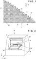
- Fig. 2 schematically shows a processing apparatus 20 that can be used to process the ZnSe member 12 in the structure ST in the processing step.
- the processing apparatus 20 is, for example, a high-precision processing machine capable of numerically controlling cutting processing on the order of several tens of nm, and the tool used in the processing apparatus 20 includes a diamond bite 22 having a sharp tip end and capable of obtaining a highly accurate processing transfer property.
- the processing apparatus 20 includes an X-Y stage arranged in a high-rigidity housing 21 strong against external vibration.
- the X-Y stage is formed by an X stage 25 movable in the X direction and a Y stage 26 movable in the Y direction, and controls the position of the structure ST as a workpiece.
- a Z stage 27 movable in the Z direction while holding the diamond bite 22 is arranged in the housing 21.
- the Z stage 27 may be provided with a rotating mechanism for rotating the diamond bite 22.
- Fig. 3 schematically shows how the processing apparatus 20 processes the ZnSe member 12 of the structure ST.
- the processing apparatus 20 includes ridgeline cutting edges 23 and 24 that define a cross-sectional shape to be transferred to the ZnSe member 12, and an angle ⁇ 2 formed by the tip ends of the ridgeline cutting edges 23 and 24 is almost equal to an opening angle ⁇ 1 of a groove forming the diffraction grating 17, which is, for example, 85° to 90°.
- the roundness of each of the tip ends of the ridgeline cutting edges 23 and 24 should be as small as possible.
- the straight line accuracy of each of the ridgelines of the ridgeline cutting edges 23 and 24 is very high at the tip end portion.
- the structure ST can be driven by the X-Y stage in a state in which the diamond bite 22 is lowered onto the structure ST so that the amount of cutting in a depth direction (Z direction) is, for example, 0.1 ⁇ m at a position where the diamond bite 22 and the structure ST as a workpiece face each other.
- the ZnSe member 12 of the structure ST undergoes cutting at the cutting speed based on the relative movement of the diamond bite 22 and the structure ST.
- the relative movement may be performed by moving the diamond bite 22.
- the total cutting amount in the Z direction may be divided and the cutting with the divided cutting amount may be repeated. Further, the diamond bite 22 may be rotated in accordance with cutting conditions.
- the relative movement speed may be reduced to suppress the load onto the diamond bite 22.
- oil mist is sprayed from the back side of the bite rake face to remove the processing heat and smoothly flow the chips.
- the structure ST in which the ZnS member 11 and the ZnSe member 12 are coupled to each other is prepared, and the ZnSe member 12 of the structure ST is processed to form the diffraction grating 17 on the ZnSe member 12.
- the diffraction device 1 can be preferably incorporated in an optical system of a spectroscopic apparatus that can spectrally disperse light in the infrared range.
- Fig. 4 schematically shows a diffraction device 1' as an application example of the above-described embodiment. Matters not mentioned regarding the diffraction device 1' can follow the description regarding the diffraction device 1.
- the diffraction device 1' includes a structure ST' including the ZnS member 11, and the ZnSe member 12 and a ZnSe member 18 coupled to the ZnS member 11.
- the first ZnSe member 12 is coupled to the first face S1 of the ZnS member 11.
- the diffraction grating 17 is provided on the ZnSe member 12.
- the second ZnSe member 18 is coupled to the second face S2 of the ZnS member 11.
- a second diffraction grating 19 is provided on the second ZnSe member 18.
- the first diffraction grating 17 and the second diffraction grating 19 can be arranged such that the periodic direction of the first diffraction grating 17 and the periodic direction of the second diffraction grating 19 are orthogonal to each other. According to such an arrangement, when the diffraction orders of the first diffraction grating 17 are output in a state in which a plurality of the orders are overlapped with each other, the second diffraction grating 19 can separate them in the order direction.
- the grating interval of the second diffraction grating 19 can be set smaller than the grating interval of the first diffraction grating 17. Conversely, the grating interval of the first diffraction grating 17 can be set larger than the grating interval of the second diffraction grating 19.
- the immersion diffraction device In the immersion diffraction device, diffraction is performed in a material having a higher refractive index (n) than that of a general reflective diffraction device (diffraction grating), so that the spectral wavelength is shortened in the material in inverse proportion to the refractive index (n). Therefore, if the immersion diffraction device has the same size as the reflective diffraction device, it can obtain a high resolution in proportion to the refractive index (n). Conversely, if the immersion diffraction device has the same resolution as the reflective diffraction device, its size can be decreased to 1/n.
- a spectroscopic apparatus incorporating the immersion diffraction device manufactured in accordance with the above-described method can have an excellent resolution or a compactness due to the immersion effect, and an excellent efficiency due to a good material transmittance and a good diffraction grating.
- Fig. 5 shows the arrangement of a spectroscopic apparatus 100 according to an embodiment of the present invention.
- the spectroscopic apparatus 100 can be referred to as an immersion spectroscopic apparatus.
- a light beam that spreads from a light guide unit 51 which can be formed by a slit or an optical fiber into which light to be spectrally dispersed enters, is collimated by a collimator 52, and can be spectrally dispersed by an immersion grating 53 (corresponding to the immersion diffraction device 1).
- the immersion grating 53 can be configured as a high-order diffraction device.
- a cross disperser 54 (a diffraction device that diffracts light in a direction orthogonal to the diffraction direction of the immersion grating 53) can be arranged downstream of the immersion grating 53.
- the diffracted light from the cross disperser 54 is deployed in a two-dimensional space for each wavelength, imaged on the light receiving face of an optical sensor 57 by condensing optical systems 55 and 56, and captured by the optical sensor 57.
- the immersion diffraction device 1 As the immersion grating 53, due to the above-described immersion effect, it is possible to implement, for example, a resolution more than twice that of the conventional resolution, or a reduction in size to 1/2 with the same resolution. Further, in the immersion diffraction device, the diffraction angle is suppressed in accordance with the refractive index in the material that forms the immersion diffraction device. Therefore, unlike the reflective diffraction device which generates a desired diffraction angle in the face to spread light, the spread of light is relatively suppressed until the emission portion, and the light is spread to a desired divergence angle at the emission portion. Such advantages are useful in implementing a compact and excellent spectroscopic apparatus.
- Fig. 6 shows the arrangement of a spectroscopic apparatus 100' according to another embodiment of the present invention.
- the spectroscopic apparatus 100' employs the immersion diffraction device 1' shown in Fig. 4 as the immersion grating 53 and the cross disperser 54 in the spectroscopic apparatus 100 shown in Fig. 5 . That is, the immersion diffraction device 1' can have the functions of the immersion grating 53 and the cross disperser 54. Note that when a reflective diffraction device is employed, the immersion diffraction device 1' cannot have the function of the cross disperser.
- the spectroscopic apparatus shown in each of Figs. 5 and 6 is merely an exemplary spectroscopic apparatus, so that details such as the number of mirrors depend on the design, and the spectroscopic apparatus of the present invention is not limited thereto.
- the optical sensor 57 may be an image sensor, a line sensor, or a single light-receiving device. If the diffraction device is a first-order diffraction device, the cross disperser is unnecessary.
- a diffraction device includes a ZnS member and a ZnSe member coupled to the ZnS member, and a diffraction grating is provided on the ZnSe member.
Landscapes
- Physics & Mathematics (AREA)
- General Physics & Mathematics (AREA)
- Optics & Photonics (AREA)
- Spectroscopy & Molecular Physics (AREA)
- Engineering & Computer Science (AREA)
- Manufacturing & Machinery (AREA)
- Diffracting Gratings Or Hologram Optical Elements (AREA)
- Spectrometry And Color Measurement (AREA)
Applications Claiming Priority (1)
| Application Number | Priority Date | Filing Date | Title |
|---|---|---|---|
| JP2019135679A JP2021018392A (ja) | 2019-07-23 | 2019-07-23 | 回折素子および分光装置、ならびに回折素子の製造方法 |
Publications (1)
| Publication Number | Publication Date |
|---|---|
| EP3770655A1 true EP3770655A1 (de) | 2021-01-27 |
Family
ID=71527657
Family Applications (1)
| Application Number | Title | Priority Date | Filing Date |
|---|---|---|---|
| EP20184701.9A Withdrawn EP3770655A1 (de) | 2019-07-23 | 2020-07-08 | Beugungsvorrichtung, spektroskopische vorrichtung und verfahren zur herstellung einer beugungsvorrichtung |
Country Status (4)
| Country | Link |
|---|---|
| US (1) | US11520090B2 (de) |
| EP (1) | EP3770655A1 (de) |
| JP (1) | JP2021018392A (de) |
| CN (1) | CN112285815A (de) |
Families Citing this family (1)
| Publication number | Priority date | Publication date | Assignee | Title |
|---|---|---|---|---|
| WO2023058474A1 (ja) * | 2021-10-05 | 2023-04-13 | 日本電気硝子株式会社 | イマージョン回折素子及びその製造方法 |
Citations (2)
| Publication number | Priority date | Publication date | Assignee | Title |
|---|---|---|---|---|
| JP2003075622A (ja) | 2001-09-05 | 2003-03-12 | Toshiba Corp | 回折格子、回折格子の加工方法及び光学要素 |
| US20130342909A1 (en) * | 2012-06-20 | 2013-12-26 | Canon Kabushiki Kaisha | Method of manufacturing a diffraction grating |
Family Cites Families (11)
| Publication number | Priority date | Publication date | Assignee | Title |
|---|---|---|---|---|
| US5243583A (en) * | 1989-04-06 | 1993-09-07 | Ricoh Company, Ltd. | Optical pickup device with dual grating element |
| JPH0611616A (ja) * | 1992-04-28 | 1994-01-21 | Hitachi Ltd | 光偏光素子 |
| JP2003006891A (ja) | 2001-06-21 | 2003-01-10 | Sankyo Seiki Mfg Co Ltd | 光ピックアップ装置 |
| US6965475B2 (en) * | 2003-03-28 | 2005-11-15 | Sumitomo Electric Industries, Ltd. | Optical component, optical device and optical communications system |
| JP2006220705A (ja) * | 2005-02-08 | 2006-08-24 | Sumitomo Electric Ind Ltd | 赤外線ハイブリッドレンズ及び赤外線ハイブリッドレンズの製造方法 |
| CN101222009A (zh) | 2007-01-12 | 2008-07-16 | 清华大学 | 发光二极管 |
| KR20090105747A (ko) | 2008-04-03 | 2009-10-07 | 삼성전자주식회사 | 광주사장치 및 이를 채용한 화상형성장치 |
| JP5599175B2 (ja) * | 2009-10-06 | 2014-10-01 | ジェイディーエス ユニフェイズ コーポレーション | 分散素子、分光装置、及び波長選択スイッチ |
| JP6254804B2 (ja) * | 2013-09-20 | 2017-12-27 | 株式会社タムロン | 赤外線光学系 |
| WO2015168182A1 (en) * | 2014-04-28 | 2015-11-05 | Finisar Corporation | Reflective diffraction gratings employing efficiency enhancement or etch barrier layers |
| JP6253724B2 (ja) * | 2016-07-08 | 2017-12-27 | キヤノン株式会社 | 反射型回折素子 |
-
2019
- 2019-07-23 JP JP2019135679A patent/JP2021018392A/ja active Pending
-
2020
- 2020-07-08 EP EP20184701.9A patent/EP3770655A1/de not_active Withdrawn
- 2020-07-15 US US16/929,543 patent/US11520090B2/en active Active
- 2020-07-23 CN CN202010718667.0A patent/CN112285815A/zh active Pending
Patent Citations (2)
| Publication number | Priority date | Publication date | Assignee | Title |
|---|---|---|---|---|
| JP2003075622A (ja) | 2001-09-05 | 2003-03-12 | Toshiba Corp | 回折格子、回折格子の加工方法及び光学要素 |
| US20130342909A1 (en) * | 2012-06-20 | 2013-12-26 | Canon Kabushiki Kaisha | Method of manufacturing a diffraction grating |
Non-Patent Citations (4)
| Title |
|---|
| DALI LIU ET AL: "Optical bistability in ZnS/ZnSe stratified grating wave filter", PROCEEDINGS OF SPIE, vol. 4602, 16 October 2001 (2001-10-16), 1000 20th St. Bellingham WA 98225-6705 USA, pages 166, XP055751987, ISSN: 0277-786X, ISBN: 978-1-5106-3927-0, DOI: 10.1117/12.445723 * |
| NAOTO KOBAYASHI: "Zinc sulfide and zinc selenide immersion gratings for astronomical high-resolution spectroscopy: evaluation of internal attenuation of bulk materials in the short near-infrared region", OPTICAL ENGINEERING, vol. 48, no. 8, 1 August 2009 (2009-08-01), pages 084001, XP055076773, ISSN: 0091-3286, DOI: 10.1117/1.3206734 * |
| PAUL J. KUZMENKO: "Prospects for machined immersion gratings in the near infrared and visible", PROCEEDINGS OF SPIE, vol. 6273, 14 June 2006 (2006-06-14), 1000 20th St. Bellingham WA 98225-6705 USA, pages 62733S, XP055751949, ISSN: 0277-786X, ISBN: 978-1-5106-3927-0, DOI: 10.1117/12.670519 * |
| ROMAN V. KRUZELECKY ET AL: "Hadamard spectrometer for passive LWIR standoff surveillance", PROCEEDINGS OF SPIE, vol. 6796, 21 June 2007 (2007-06-21), 1000 20th St. Bellingham WA 98225-6705 USA, pages 67962I, XP055751967, ISSN: 0277-786X, ISBN: 978-1-5106-3927-0, DOI: 10.1117/12.778911 * |
Also Published As
| Publication number | Publication date |
|---|---|
| US20210026052A1 (en) | 2021-01-28 |
| US11520090B2 (en) | 2022-12-06 |
| CN112285815A (zh) | 2021-01-29 |
| JP2021018392A (ja) | 2021-02-15 |
Similar Documents
| Publication | Publication Date | Title |
|---|---|---|
| JP5864920B2 (ja) | 回折格子の製造方法 | |
| EP2677350B1 (de) | Verfahren zur Herstellung eines Diffraktionsgitters | |
| EP0254453A2 (de) | Diskretes optisches Gitter und Vorrichtung | |
| JP6032869B2 (ja) | ブレーズ型回折格子 | |
| EP3770655A1 (de) | Beugungsvorrichtung, spektroskopische vorrichtung und verfahren zur herstellung einer beugungsvorrichtung | |
| JP2003075622A (ja) | 回折格子、回折格子の加工方法及び光学要素 | |
| US20150177428A1 (en) | Diffraction grating and diffraction grating producing method | |
| JP6253724B2 (ja) | 反射型回折素子 | |
| US9372289B2 (en) | Method of manufacturing a diffraction grating | |
| JP5972100B2 (ja) | 反射型回折素子 | |
| JP2017156589A (ja) | ブレーズ型回折格子、製造方法、分光装置及び伝送装置 | |
| US12030143B2 (en) | Method for manufacturing a cutting tool, and the cutting tool | |
| CN111741839B (zh) | 模具的制造方法 | |
| JP2020112601A (ja) | 回折素子、分光分析装置、回折素子の製造方法 | |
| Yamagata et al. | Fabrication of blazed holographic optical element by ultrahigh-precision cutting |
Legal Events
| Date | Code | Title | Description |
|---|---|---|---|
| PUAI | Public reference made under article 153(3) epc to a published international application that has entered the european phase |
Free format text: ORIGINAL CODE: 0009012 |
|
| STAA | Information on the status of an ep patent application or granted ep patent |
Free format text: STATUS: THE APPLICATION HAS BEEN PUBLISHED |
|
| AK | Designated contracting states |
Kind code of ref document: A1 Designated state(s): AL AT BE BG CH CY CZ DE DK EE ES FI FR GB GR HR HU IE IS IT LI LT LU LV MC MK MT NL NO PL PT RO RS SE SI SK SM TR |
|
| AX | Request for extension of the european patent |
Extension state: BA ME |
|
| STAA | Information on the status of an ep patent application or granted ep patent |
Free format text: STATUS: REQUEST FOR EXAMINATION WAS MADE |
|
| 17P | Request for examination filed |
Effective date: 20210727 |
|
| RBV | Designated contracting states (corrected) |
Designated state(s): AL AT BE BG CH CY CZ DE DK EE ES FI FR GB GR HR HU IE IS IT LI LT LU LV MC MK MT NL NO PL PT RO RS SE SI SK SM TR |
|
| GRAP | Despatch of communication of intention to grant a patent |
Free format text: ORIGINAL CODE: EPIDOSNIGR1 |
|
| STAA | Information on the status of an ep patent application or granted ep patent |
Free format text: STATUS: GRANT OF PATENT IS INTENDED |
|
| RIC1 | Information provided on ipc code assigned before grant |
Ipc: G01J 3/02 20060101ALI20230213BHEP Ipc: G01J 3/18 20060101ALI20230213BHEP Ipc: G02B 5/18 20060101AFI20230213BHEP |
|
| INTG | Intention to grant announced |
Effective date: 20230320 |
|
| RIN1 | Information on inventor provided before grant (corrected) |
Inventor name: SUKEGAWA, TAKASHI |
|
| STAA | Information on the status of an ep patent application or granted ep patent |
Free format text: STATUS: THE APPLICATION HAS BEEN WITHDRAWN |
|
| 18W | Application withdrawn |
Effective date: 20230525 |