EP3758170A2 - Lasertreiber mit klemmschaltung mit freilaufdiode - Google Patents
Lasertreiber mit klemmschaltung mit freilaufdiode Download PDFInfo
- Publication number
- EP3758170A2 EP3758170A2 EP20179464.1A EP20179464A EP3758170A2 EP 3758170 A2 EP3758170 A2 EP 3758170A2 EP 20179464 A EP20179464 A EP 20179464A EP 3758170 A2 EP3758170 A2 EP 3758170A2
- Authority
- EP
- European Patent Office
- Prior art keywords
- coupled
- node
- transistor
- current
- laser diode
- Prior art date
- Legal status (The legal status is an assumption and is not a legal conclusion. Google has not performed a legal analysis and makes no representation as to the accuracy of the status listed.)
- Withdrawn
Links
Images




Classifications
-
- H—ELECTRICITY
- H01—ELECTRIC ELEMENTS
- H01S—DEVICES USING THE PROCESS OF LIGHT AMPLIFICATION BY STIMULATED EMISSION OF RADIATION [LASER] TO AMPLIFY OR GENERATE LIGHT; DEVICES USING STIMULATED EMISSION OF ELECTROMAGNETIC RADIATION IN WAVE RANGES OTHER THAN OPTICAL
- H01S5/00—Semiconductor lasers
- H01S5/04—Processes or apparatus for excitation, e.g. pumping, e.g. by electron beams
- H01S5/042—Electrical excitation ; Circuits therefor
- H01S5/0428—Electrical excitation ; Circuits therefor for applying pulses to the laser
-
- H—ELECTRICITY
- H01—ELECTRIC ELEMENTS
- H01S—DEVICES USING THE PROCESS OF LIGHT AMPLIFICATION BY STIMULATED EMISSION OF RADIATION [LASER] TO AMPLIFY OR GENERATE LIGHT; DEVICES USING STIMULATED EMISSION OF ELECTROMAGNETIC RADIATION IN WAVE RANGES OTHER THAN OPTICAL
- H01S5/00—Semiconductor lasers
- H01S5/04—Processes or apparatus for excitation, e.g. pumping, e.g. by electron beams
- H01S5/042—Electrical excitation ; Circuits therefor
-
- H—ELECTRICITY
- H01—ELECTRIC ELEMENTS
- H01S—DEVICES USING THE PROCESS OF LIGHT AMPLIFICATION BY STIMULATED EMISSION OF RADIATION [LASER] TO AMPLIFY OR GENERATE LIGHT; DEVICES USING STIMULATED EMISSION OF ELECTROMAGNETIC RADIATION IN WAVE RANGES OTHER THAN OPTICAL
- H01S5/00—Semiconductor lasers
- H01S5/04—Processes or apparatus for excitation, e.g. pumping, e.g. by electron beams
- H01S5/042—Electrical excitation ; Circuits therefor
- H01S5/0427—Electrical excitation ; Circuits therefor for applying modulation to the laser
-
- H—ELECTRICITY
- H01—ELECTRIC ELEMENTS
- H01S—DEVICES USING THE PROCESS OF LIGHT AMPLIFICATION BY STIMULATED EMISSION OF RADIATION [LASER] TO AMPLIFY OR GENERATE LIGHT; DEVICES USING STIMULATED EMISSION OF ELECTROMAGNETIC RADIATION IN WAVE RANGES OTHER THAN OPTICAL
- H01S5/00—Semiconductor lasers
- H01S5/06—Arrangements for controlling the laser output parameters, e.g. by operating on the active medium
- H01S5/062—Arrangements for controlling the laser output parameters, e.g. by operating on the active medium by varying the potential of the electrodes
- H01S5/06209—Arrangements for controlling the laser output parameters, e.g. by operating on the active medium by varying the potential of the electrodes in single-section lasers
- H01S5/06216—Pulse modulation or generation
-
- H—ELECTRICITY
- H01—ELECTRIC ELEMENTS
- H01S—DEVICES USING THE PROCESS OF LIGHT AMPLIFICATION BY STIMULATED EMISSION OF RADIATION [LASER] TO AMPLIFY OR GENERATE LIGHT; DEVICES USING STIMULATED EMISSION OF ELECTROMAGNETIC RADIATION IN WAVE RANGES OTHER THAN OPTICAL
- H01S5/00—Semiconductor lasers
- H01S5/06—Arrangements for controlling the laser output parameters, e.g. by operating on the active medium
- H01S5/068—Stabilisation of laser output parameters
- H01S5/06825—Protecting the laser, e.g. during switch-on/off, detection of malfunctioning or degradation
-
- H—ELECTRICITY
- H03—ELECTRONIC CIRCUITRY
- H03K—PULSE TECHNIQUE
- H03K17/00—Electronic switching or gating, i.e. not by contact-making and –breaking
- H03K17/08—Modifications for protecting switching circuit against overcurrent or overvoltage
- H03K17/081—Modifications for protecting switching circuit against overcurrent or overvoltage without feedback from the output circuit to the control circuit
- H03K17/0814—Modifications for protecting switching circuit against overcurrent or overvoltage without feedback from the output circuit to the control circuit by measures taken in the output circuit
- H03K17/08142—Modifications for protecting switching circuit against overcurrent or overvoltage without feedback from the output circuit to the control circuit by measures taken in the output circuit in field-effect transistor switches
-
- H—ELECTRICITY
- H03—ELECTRONIC CIRCUITRY
- H03K—PULSE TECHNIQUE
- H03K17/00—Electronic switching or gating, i.e. not by contact-making and –breaking
- H03K17/10—Modifications for increasing the maximum permissible switched voltage
- H03K17/102—Modifications for increasing the maximum permissible switched voltage in field-effect transistor switches
-
- G—PHYSICS
- G01—MEASURING; TESTING
- G01S—RADIO DIRECTION-FINDING; RADIO NAVIGATION; DETERMINING DISTANCE OR VELOCITY BY USE OF RADIO WAVES; LOCATING OR PRESENCE-DETECTING BY USE OF THE REFLECTION OR RERADIATION OF RADIO WAVES; ANALOGOUS ARRANGEMENTS USING OTHER WAVES
- G01S7/00—Details of systems according to groups G01S13/00, G01S15/00, G01S17/00
- G01S7/48—Details of systems according to groups G01S13/00, G01S15/00, G01S17/00 of systems according to group G01S17/00
- G01S7/483—Details of pulse systems
- G01S7/484—Transmitters
-
- H—ELECTRICITY
- H01—ELECTRIC ELEMENTS
- H01S—DEVICES USING THE PROCESS OF LIGHT AMPLIFICATION BY STIMULATED EMISSION OF RADIATION [LASER] TO AMPLIFY OR GENERATE LIGHT; DEVICES USING STIMULATED EMISSION OF ELECTROMAGNETIC RADIATION IN WAVE RANGES OTHER THAN OPTICAL
- H01S5/00—Semiconductor lasers
- H01S5/06—Arrangements for controlling the laser output parameters, e.g. by operating on the active medium
- H01S5/062—Arrangements for controlling the laser output parameters, e.g. by operating on the active medium by varying the potential of the electrodes
- H01S5/06226—Modulation at ultra-high frequencies
Definitions
- This application is directed to the field of laser driving, and in particular, is directed to a circuit for generating pulses (based upon which a laser diode is driven) having a desired pulse width, by underdamping a laser driver and using clamping to dampen oscillations occurring upon turn-off of the laser driver.
- Time-of-flight ranging applications such as Light Detection and Ranging (LIDAR)
- LIDAR Light Detection and Ranging
- a laser diode typically infrared
- the laser pulse is reflected by a (possible) object in that given direction, and a receiver receives and reads the reflected laser pulse.
- the receiver with a proper timing reference, measures the elapsed time between emitting the laser pulse and receiving the reflected laser pulse. From this elapsed time, the distance to the object can be evaluated.
- An optical pulse on the order of Ins is therefore not useful if it is desired to discriminate distances below 60cm with accuracy.
- the pulse width of the optical pulse is related to the pulse width of the pulsed drive current, it is therefore desired to be able to produce a pulsed drive current having a shorter pulse width so that the pulse width of the laser pulses can be reduced to thereby increase accuracy and enable discrimination of even shorter distances.
- a conventional laser diode does not immediately turn-on and lase (emit laser light) when driven by the pulsed drive current, there is a turn-on time. Since the turn-on time reduces the repetition rate of the laser pulses, it is also desired to decrease the turn-on time.
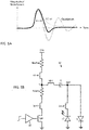
- FIG. 1A Shown in the graph of FIG. 1A is a drive current for a laser diode over time.
- a laser diode To cause a laser diode to emit a laser pulse, it is desired to drive it with a sharp narrow drive pulse for spatial accuracy when making a ranging measurement.
- designing a laser driver involves certain tradeoffs. The narrower the drive pulse, the sharper its rise and fall. Too sharp of a fall can cause “ringing", by which the drive current of the drive pulse oscillates (shown by the dashed line labeled as "Oscillation"), potentially with enough magnitude to cause emission of a second unplanned laser pulse, which is undesirable for any ranging application (whether time of flight or LIDAR).
- a drive pulse can be shaped so as to have a sharp rise and slow fall (shown by the dashed line labeled as "Slow"), a slow fall can impact efficiency, and is therefore undesirable. Therefore, it is now known to dampen (but not widen) the fall of the drive pulse, producing the pulse shown with a solid line.
- the laser driver circuit 10 includes a driver amplifier 11 that receives a trigger pulse, and, responsive to an edge of the trigger pulse (for example, the rising edge), drives a switch SW.
- the pulse width of the laser produced by the laser driver circuit 10 is not sensitive to the pulse width of the trigger pulse, but is simply edge sensitive.
- the switch SW is an n-channel MOS transistor having its source coupled to ground and its gate biased by the driver amplifier 11. While the switch SW is illustrated as an NMOS transistor, it could instead be an avalanche transistor (e.g., a bipolar transistor operating in avalanche breakdown).
- An illustrated inductance Lp,sw is shown as coupled between the drain of the switch SW and node N, and represents the sum of series parasitic inductances between the drain of the switch SW and node N (e.g., the parasitic inductance of the PCB traces between the drain of the switch SW and node N, and the parasitic inductance of resistor Rclamp).
- An illustrated inductance Lp,up is shown as coupled between node N and a pull up resistor Rpullup, and represents the sum of series parasitic inductances between node N and VHV (e.g., the parasitic inductance of the PCB traces between node N and VHV, and the parasitic inductance of the resistor Rpullup).
- the pull up resistor Rpullup is coupled between node N and the high voltage supply node VHV.
- the clamping resistor Rclamp is coupled between the drain of the switch SW and node N.
- a laser diode LD has its anode coupled to ground and its cathode coupled to the output node OUT through an illustrated parasitic inductance Lp,Ld.
- the illustrated parasitic inductance Lp,Ld is coupled between the cathode of the laser diode LD and the output node OUT, and represents a sum of the parasitic inductances in series to the laser diode LD between ground and the output node OUT (e.g., the parasitic inductance of the PCB traces between ground and the output node OUT, and the parasitic inductance of the laser diode LD itself).
- a diode D has its anode coupled to the output node OUT and its cathode coupled to ground.
- a capacitor C is coupled between the output node OUT and node N through an illustrated parasitic inductance Lp,c.
- the parasitic inductance Lp,c represents a sum of the parasitic inductances in series between the output node OUT and node N (e.g., the parasitic inductance of the PCB traces between node OUT and node N, and the parasitic inductance of the capacitor C).
- a positive voltage across the laser diode LD results (meaning that the voltage at the anode of the laser diode LD exceeds the voltage at the cathode of the laser diode LD), and the laser diode LD turns on and a current will flow from ground through laser diode LD to the capacitor C.
- the capacitor C will be discharged by the current from ground.
- the output node OUT therefore will increase from -VHV to ground, automatically switching off the laser diode LD when its forward voltage (voltage from anode to cathode) falls sufficiently. Viewed at first order, this switching off of the laser diode LD occurs regardless of whether the trigger pulse has transitioned back low or not.
- the RLC components of the laser driver circuit 10 so described therefore (if sized accordingly to accurate criteria) work like a properly damped system. Looking at the drive current (the current flowing through the laser diode LD) as shown in FIG. 1A , this leads to a high initial high spike, followed by an exponential decay.
- the capacitor C will be re-charged from the high voltage supply node VHV through the resistor Rpullup and diode D.
- the repetition rate of the laser driver circuit 10 is therefore limited by the recovery time of the capacitor C (e.g., the time needed to be charged back to the voltage VHV).
- the laser driver circuit 10 is damped. This means that, as previously described, the laser drive current through the laser diode LD will have a fast rising edge and a fast exponentially decay as a falling edge. Ringing is not present, preventing the laser diode LD from lasing multiple times in response to a single trigger pulse.
- the total inductance Ltot can be lowered, as can be seen from the above equations. However, this is not necessarily possible due to the parasitic inductances present in the laser driver circuit 10.
- the capacitance of capacitor C plays an opposite role to the total inductance Ltot - the capacitance is to be reduced to enable production of a narrow pulse. However, this leads to a reduced Ipeak value for the laser drive current through the laser diode LD.
- the greater the capacitance of the capacitor C the greater the recovery time of the laser driver circuit 10.
- the peak current Ipeak through the laser diode LD is dependent on VHV, and it is undesirable to increase VHV past a certain point to maintain safe operating area (SOA). It is possible to reduce recovery time by reducing the resistance of the pull up resistor Rpullup. However, this will increase power consumption.
- a circuit including a laser diode having an anode coupled to a high voltage supply node and a cathode coupled to an output node, a current source coupled between the output node and ground, and at least one clamping circuit coupled between the output node and the high voltage supply node.
- the current source is configured to turn on in response to a first logic state of a trigger signal and sink current from the high voltage supply node to ground to thereby cause the laser diode to lase, and is configured to turn off in response to a second logic state of the trigger signal.
- the at least one clamping circuit is configured to clamp voltage at the output node occurring in response to switching of the current source from turned on to turned off.
- the current source may include a current generator transistor having a first conduction terminal, a second conduction terminal coupled to ground, and a control terminal coupled to a bias voltage, a switching transistor having a first conduction terminal, a second conduction terminal coupled to the first conduction terminal of the current generator transistor, and a control terminal coupled to receive the trigger signal, and a cascode transistor having a first conduction terminal coupled to the output node, a second conduction terminal coupled to the first conduction terminal of the switching transistor, and a gate coupled to a bias voltage.
- the current generator transistor may include a first n-channel transistor having a source coupled to ground, a drain, and a gate coupled to the bias voltage.
- the switching transistor may include a second n-channel transistor having a source coupled to the drain of the current generator transistor, a drain, and a gate coupled to receive the trigger signal.
- the cascode transistor may include a third n-channel transistor having a source coupled to the drain of the switching transistor, a drain coupled to the output node, and a gate coupled to the bias voltage.
- the at least one clamping circuit may include a first diode having an anode coupled to the output node and a cathode coupled to a first node, a resistor coupled between the first node and a second node, a second diode having an anode coupled to the second node and a cathode coupled to the high voltage supply node, and a switch transistor having a first conduction terminal coupled to the second node, a second conduction terminal coupled to the first node, and a control terminal coupled to the second node through a Zener diode and to the first node through a capacitor (which is parasitic, but a discrete capacitor may additionally be used in some cases).
- a capacitor which is parasitic, but a discrete capacitor may additionally be used in some cases.
- the switch transistor may include a fourth n-channel transistor having a drain coupled to the first node, a source coupled to the second node, and a gate coupled to the second node through the Zener diode and to the first node through the capacitor .
- the at least one clamping circuit may include a selection transistor having a first conduction terminal coupled to the control terminal of the switch transistor, a second conduction terminal coupled to ground, and a gate coupled to a control signal.
- the selection transistor may include a fifth n-channel transistor having a drain coupled to the gate of the switch transistor, a source coupled to ground, and a gate coupled to the control signal.
- the control terminal of the switch transistor may be coupled to the second node through the Zener diode having an anode coupled to the second node and a cathode coupled to the control terminal of the switch transistor.
- the at least one clamping circuit may include a plurality of clamping circuits coupled in parallel between the output node and the high voltage supply node, each of the plurality of clamping circuits being selectable so as to permit a desired number of the plurality of clamping circuits to be enabled while a remainder of the plurality of clamping circuits remain disabled.
- a clamping circuit including a first diode having an anode coupled to an output node and a cathode coupled to a first node, a resistor coupled between the first node and a second node, a second diode having an anode coupled to the second node and a cathode coupled to a high voltage supply node, and a switch transistor having a first conduction terminal coupled to the second node, a second conduction terminal coupled to the first node, and a control terminal coupled to the second node through a Zener diode and to the first node through a capacitance (which is parasitic, but a discrete capacitor may additionally be used in some cases).
- a capacitance which is parasitic, but a discrete capacitor may additionally be used in some cases.
- the switch transistor may include a fourth n-channel transistor having a drain coupled to the first node, a source coupled to the second node, and a gate coupled to the second node through the Zener diode and to the first node through the capacitance.
- a selection transistor may have a first conduction terminal coupled to the control terminal of the switch transistor, a second conduction terminal coupled to ground, and a gate coupled to a control signal.
- the selection transistor may include a fifth n-channel transistor having a drain coupled to the gate of the switch transistor, a source coupled to ground, and a gate coupled to the control signal.
- the control terminal of the switch transistor may be coupled to the second node through the Zener diode having an anode coupled to the second node and a cathode coupled to the control terminal of the switch transistor.
- Also disclosed herein is a method including turning on a current source of an underdamped laser driver arranged so that when the current source turns on to cause sinking of current from a laser diode coupled between a high voltage node and an output node, a first current overshoot occurs in the laser diode results in lasing of the laser diode.
- the method also includes turning off a current source to stop sinking of current from the laser diode by the current source, and to cause a first current undershoot in the laser diode and a first voltage overshoot at the output node.
- the method further includes after the first current overshoot and in response to the first current undershoot, turning on a clamping circuit with the first voltage overshoot to thereby dampen voltage at the output node.
- the clamping circuit may be turned on if the first voltage overshoot is sufficiently high such that an attenuated version of the first voltage overshoot appearing at the gate of a transistor turns on the transistor, and if sufficient voltage headroom between the voltage at the output node and the high voltage node exists to turn on a first diode coupled between the output node and a drain of the transistor and to turn on a second diode coupled between a source of the transistor and the high voltage supply node.
- the method may include reducing turn-on time of the laser diode by turning on an additional current source to sink a threshold current from the laser diode a threshold time prior to turning on of the additional current source, the threshold current biasing the laser diode to near, but below, a lasing region, and turning off the additional current source the threshold time after turning off of the current source.
- a clamping circuit including a first diode having an anode directly electrically connected to an output node and a cathode directly electrically connected to a first node, a resistor directly electrically connected between the first node and a second node, a second diode having an anode directly electrically connected to the second node and a cathode directly electrically connected coupled to a high voltage supply node, and a switch transistor having a first conduction terminal directly electrically connected to the second node, a second conduction terminal directly electrically connected to the first node, and a control terminal coupled to the second node through a Zener diode and to the first node through a capacitor (which is parasitic, but a discrete capacitor may additionally be used in some cases).
- the switch transistor may include a fourth n-channel transistor having a drain directly electrically connected to the first node, a source directly electrically connected to the second node, and a gate coupled to the second node through the Zener diode and to the first node through the capacitor.
- a selection transistor may have a first conduction terminal directly electrically connected to the control terminal of the switch transistor, a second conduction terminal directly electrically connected to ground, and a gate directly electrically connected to a control signal.
- the selection transistor may include a fifth n-channel transistor having a drain directly electrically connected to the gate of the switch transistor, a source directly electrically connected to ground, and a gate directly electrically connected to the control signal.
- the control terminal of the switch transistor may be directly electrically connected to the second node through the Zener diode having an anode directly electrically connected to the second node and a cathode directly electrically connected to the control terminal of the switch transistor.
- an integrated circuit chip including a high voltage supply input pin, a supply voltage input pin, a laser diode anode pin for connection to an anode of an external laser diode, a laser diode cathode pin for connection to a cathode of the external laser diode, a current source coupled between an laser diode cathode pin and ground, the current source configured to turn on in response to a first logic state of a trigger signal and sink current from the high voltage supply input pin to ground, and configured to turn off in response to a second logic state of the trigger signal, and at least one clamping circuit coupled between the laser diode cathode pin and the high voltage supply input pin, the at least one clamping circuit configured to clamp voltage at the laser diode cathode pin occurring in response to switching of the current source from turned on to turned off.
- the current source may include a current generator transistor having a first conduction terminal, a second conduction terminal coupled to ground, and a control terminal coupled to a first bias voltage, a switching transistor having a first conduction terminal, a second conduction terminal coupled to the first conduction terminal of the current generator transistor, and a control terminal coupled to receive the trigger signal, and a cascode transistor having a first conduction terminal coupled to the laser diode cathode pin, a second conduction terminal coupled to the first conduction terminal of the switching transistor, and a gate coupled to a second bias voltage.
- the current generator transistor may include a first n-channel transistor having a source coupled to ground, a drain, and a gate coupled to the bias voltage.
- the switching transistor may include a second n-channel transistor having a source coupled to the drain of the current generator transistor, a drain, and a gate coupled to receive the trigger signal.
- the cascode transistor may include a third n-channel transistor having a source coupled to the drain of the switching transistor, a drain coupled to the laser diode cathode pin, and a gate coupled to the second bias voltage.
- the at least one clamping circuit may include a first diode having an anode coupled to the laser diode cathode pin and a cathode coupled to a first node, a resistor coupled between the first node and a second node, a second diode having an anode coupled to the second node and a cathode coupled to the high voltage supply input pin, and a switch transistor having a first conduction terminal coupled to the second node, a second conduction terminal coupled to the first node, and a control terminal coupled to the second node through a Zener diode and to the first node through a capacitance (which is parasitic, but a discrete capacitor may additionally be used in some cases).
- a capacitance which is parasitic, but a discrete capacitor may additionally be used in some cases.
- the switch transistor may include a fourth n-channel transistor having a drain coupled to the first node, a source coupled to the second node, and a gate coupled to the second node through the Zener diode and to the first node through the capacitance.
- the at least one clamping circuit may include a selection transistor having a first conduction terminal coupled to the control terminal of the switch transistor, a second conduction terminal coupled to ground, and a gate coupled to a control signal.
- the selection transistor may include a fifth n-channel transistor having a drain coupled to the gate of the switch transistor, a source coupled to ground, and a gate coupled to the control signal.
- the control terminal of the switch transistor may be coupled to the second node through the Zener diode having an anode coupled to the second node and a cathode coupled to the control terminal of the switch transistor.
- the at least one clamping circuit may include a plurality of clamping circuits coupled in parallel between the laser diode cathode pin and the high voltage supply input pin, each of the plurality of clamping circuits being selectable so as to permit a desired number of the plurality of clamping circuits to be enabled while a remainder of the plurality of clamping circuits remain disabled.
- a circuit including an input node to be coupled to a cathode of a laser diode having its anode coupled to a high voltage supply node, and a cascoded current mirror having an input branch and an output branch.
- the input branch is coupled between the high voltage supply node and a sense resistor coupled to the input node
- the output branch is coupled between the high voltage supply node and an output node.
- a sense resistance is coupled between the output node and ground, with the sense resistance being a diode coupled transistor coupled to the output node and a resistor coupled between the diode coupled transistor and ground.
- the input branch is configured to generate a current proportional to a voltage drop across the laser diode.
- the output branch is configured to generate a mirrored current proportional to the current proportional to the voltage drop across the laser diode.
- a voltage proportional to the voltage drop across the laser diode is generated as a result of the mirrored current flowing through the sense resistance.
- a comparison circuit is configured to compare the voltage proportional to the voltage drop across the laser diode to a threshold voltage.
- the comparison circuit may be configured to assert a fault output if the voltage proportional to the voltage drop across the laser diode exceeds the threshold voltage for a set period of time.
- the set period of time may be at least equal to an expected duration of a laser drive current pulse.
- the comparison circuit may be configured to assert a fault flag if the voltage proportional to the voltage drop across the laser diode exceeds the threshold voltage.
- a bias setting current may be configured to bias cascode transistors of the cascoded current mirror.
- Clamp circuits may be configured to protect transistors of the cascoded current mirror against damage.
- a circuit including a cascoded current mirror having an input branch and an output branch, and a first sense resistor coupled between the first input branch and an input node.
- the input node is configured to be coupled to a cathode of a laser diode having its anode coupled to a high voltage supply node.
- An output node is coupled to the output branch.
- a sense branch is coupled between the output node and ground.
- a comparator has a first input coupled to the output node, a second input coupled to a threshold voltage, and an output generating a fault flag.
- the cascoded current mirror may include a first p-channel transistor having a drain coupled to the first sense resistor, a source, and a gate.
- a second p-channel transistor may have a drain coupled to the source of the first p-channel transistor, a source coupled to the high voltage supply node, and a gate coupled to the drain of the first p-channel transistor to define a diode configuration.
- a third p-channel transistor may have a source coupled to the high voltage supply node, a drain, and a gate coupled to the gate of the second p-channel transistor.
- a fourth p-channel transistor may have a source coupled to the drain of the third p-channel transistor, a drain coupled to the output node, and a gate coupled to the gate of the first n-channel transistor.
- a first Zener diode may have an anode coupled to the source of the first p-channel transistor and the drain of the second p-channel transistor, and a cathode coupled to the high voltage supply node.
- a second Zener diode may have an anode coupled to the gates of the second and third p-channel transistors, and a cathode coupled to the high voltage supply node.
- a third Zener diode may have an anode coupled to the source of the fourth p-channel transistor and the drain of the third p-channel transistor, and a cathode coupled to the high voltage supply node.
- a fourth Zener diode may have an anode coupled to the gates of the first and fourth p-channel transistors, and a cathode coupled to the high voltage supply node.
- a bias setting circuit may include a fifth p-channel transistor having a drain coupled to the gates of the first and fourth p-channel transistors, a source coupled to the drain of the first p-channel transistor, and a gate directly coupled to the drain of the fifth p-channel transistor and indirectly coupled to the source of the fifth p-channel transistor through a capacitor.
- a current source may generate a bias current sunk by the drain of the fifth p-channel transistor.
- the sense branch may include a diode coupled p-channel transistor having a source coupled to the output node, a drain, and a gate coupled to the drain of the diode coupled p-channel transistor.
- a second sense resistor may be coupled between the drain of the diode coupled p-channel transistor and ground.
- a fifth Zener diode may have an anode coupled to ground, and a cathode coupled to the output node.
- a digital block may include a delay block configured to receive the fault flag and to output a delayed version of the fault flag, an AND gate having a first input configured to receive the fault flag, a second input configured to receive the delayed version of the fault flag, and an output generating a clock pulse.
- the digital block may also include a flip flop having a D input coupled to a supply voltage, a clock input coupled to the output of the AND gate, a clear input coupled to a fault clear signal, and an output generating a fault output signal.
- Another method aspect disclosed herein is directed to a method of detecting faults in driving of a laser diode.
- the method includes generating a voltage proportional to a voltage drop across the laser diode, comparing the voltage proportional to the voltage drop across the laser diode to a threshold voltage, and if the voltage proportional to the voltage drop across the laser diode rises and remains above the threshold voltage for a period of time greater than an expected duration of a laser drive current pulse, indicating detection of a fault in the driving of the laser diode.
- Generating the voltage proportional to the voltage drop across the laser diode may include generating a current proportional to the voltage drop across the laser diode, and mirroring the current proportional to the voltage drop across the laser diode, across a cascoded current mirror, to produce a mirrored current.
- the voltage proportional to the voltage drop across the laser diode may be generated as being equal to a voltage drop of the mirrored current across a voltage replication circuit.
- the method may also include receiving external input setting the threshold voltage and setting the period of time.
- a level shifter including an input node capacitively coupled to a laser driver to receive a signal therefrom indicative of generation of a laser drive pulse, a first p-channel transistor having a source coupled to a supply node, a drain coupled to an output node, and a gate coupled to the input node, and an n-channel transistor having a drain coupled to the drain of the first p-channel transistor, a source coupled to ground, and a gate coupled to the input node.
- a first switch selectively couples the input node to the output node.
- the laser driver is comprised of a laser and clamp circuit that includes a laser diode and clamp, and a cascode current generator coupled to the laser and clamp circuit, the cascode current generator for causing the laser diode to lase.
- the cascode current generator includes a driver amplifier (buffer) generating a trigger pulse for a cascoded transistor switch.
- This lever shifter is adaptable to both the case where the input node of the level shifter is capacitively coupled to the output of the driver amplifier (buffer) of the cascode current generator, or where the input node of the level shifter is capacitively coupled to the drain of the cascoded transistor switch.
- the level shifter includes a second p-channel transistor has a source coupled to the supply node, a drain selectively coupled to the output node by a second switch, and a gate coupled to the input node.
- the first switch closes and the second switch opens when the signal indicative of generation of a laser drive pulse is low.
- the first switch opens and the second switch closes when the signal indicative of generation of a laser drive pulse is high.
- the level shifter includes a second n-channel transistor having a source coupled to ground, a drain selectively coupled to the output node by a second switch, and a gate coupled to the input node.
- the first switch closes and the second switch opens when the signal indicative of generation of a laser drive pulse is low.
- the first switch opens and the second switch closes when the signal indicative of generation of a laser drive pulse is high.
- a buffer may have an input coupled to the output node.
- a first current source may generate a current proportional to absolute temperature, the first current source biasing the buffer with the current proportional to absolute temperature.
- a level shifter including an input node capacitively coupled to a laser driver to receive a signal therefrom indicative of generation of a laser drive pulse, and an inverter.
- the inverter has an input coupled to the input node and an output coupled to an output node, the inverter having adjustable threshold voltage that increases when the signal on the input node goes high and decreases when the signal on the input node returns low.
- the inverter is formed from a p-channel transistor and n-channel transistor.
- the p-channel transistor has a source coupled to a supply voltage, a drain coupled to the output node, and a gate coupled to the input node.
- the n-channel transistor has a drain coupled to the output node, a source coupled to ground, and a gate coupled to the input node.
- a first switch is coupled between the input node and output node.
- a threshold altering transistor (which may be p-channel or n-channel) has its source selectively coupled to the output node by a second switch, and its gate coupled to the input node. If the threshold altering transistor is n-channel, then its drain is coupled to the supply voltage, whereas if the threshold altering transistor is p-channel, then its drain is coupled to ground.
- the threshold of the inverter is adjusted as a consequence of the switching of the first and second switches that is in turn an indirect consequence of the signal on the input node. This is an indirect consequence since, when a trigger pulse for an AC coupled laser driver is generated, an analog signal is generated and AC coupled to the input node, and it is this trigger pulse that drives the generation of a control signal for the first and second switches.
- the level shifter may include a buffer having an input coupled to the output node, and a first current source generating a current proportional to absolute temperature, the first current source biasing the buffer with the current proportional to absolute temperature.
- a time of flight ranging system including a laser diode, a laser driver configured to generate a laser drive pulse for the laser diode to cause the laser diode to generate a laser pulse, a receiver, and a level shifter.
- the level shifter includes an input node capacitively coupled to the laser driver to receive a signal therefrom indicative of generation of a laser drive pulse.
- An inverter has an input coupled to the input node and an output coupled to an output node, the inverter also having adjustable threshold voltage that increases when the signal on the input node goes high and decreases when the signal on the input node returns low.
- a time to digital converter is configured to begin counting based upon output received from the level shifter, to stop counting when the receiver detects the laser pulse after the last pulse has reflected off an object, and to determine a distance to the object based upon the count.
- the laser driver is comprised of a laser and clamp circuit that includes a laser diode and clamp, and a cascode current generator coupled to the laser and clamp circuit, the cascode current generator for causing the laser diode to lase.
- the cascode current generator includes a driver amplifier (buffer) generating a trigger pulse for a cascoded transistor switch.
- This time of flight ranging system is adaptable to both the case where the input node of the level shifter is capacitively coupled to the output of the driver amplifier (buffer) of the cascode current generator, or where the input node of the level shifter is capacitively coupled to the drain of the cascoded transistor switch.
- the inverter includes a first p-channel transistor having a source coupled to a supply node, a drain coupled to the output node, and a gate coupled to the input node, and an n-channel transistor having a drain coupled to the drain of the first p-channel transistor, a source coupled to ground, and a gate coupled to the input node.
- a first switch selectively couples the input node to the output node.
- a second p-channel transistor has a source coupled to the supply node, a drain selectively coupled to the output node by a second switch, and a gate coupled to the input node. The first switch closes and the second switch opens when the signal indicative of generation of a laser drive pulse is low. The first switch opens and the second switch closes when the signal indicative of generation of a laser drive pulse is high.
- the inverter includes a first p-channel transistor having a source coupled to a supply node, a drain coupled to the output node, and a gate coupled to the input node, and an n-channel transistor having a drain coupled to the drain of the first p-channel transistor, a source coupled to ground, and a gate coupled to the input node.
- a first switch selectively couples the input node to the output node.
- a second n-channel transistor has a source coupled to ground, a drain selectively coupled to the output node by a second switch, and a gate coupled to the input node. The first switch closes and the second switch opens when the signal indicative of generation of a laser drive pulse is low. The first switch opens and the second switch closes when the signal indicative of generation of a laser drive pulse is high.
- the threshold of the inverter is adjusted as a consequence of the switching of the first and second switches that is in turn an indirect consequence of the signal on the input node. This is an indirect consequence since, when the trigger pulse is generated, an analog signal is generated and AC coupled to the input node, and it is this trigger pulse that drives the generation of a control signal for the first and second switches.
- a buffer may have an input coupled to the output node.
- a first current source may generate a current proportional to absolute temperature, the first current source biasing the buffer with the current proportional to absolute temperature.
- Also disclosed herein is a method of operating a level shifter capacitively coupled to a laser driver.
- the method includes in a steady state, coupling an input and an output of an inverter within the level shifter to one another to thereby set the input and output of the inverter to a threshold voltage.
- the method also includes when a signal from the laser driver goes high, increasing the threshold voltage of the inverter to protect the input of the inverter from noise. When the signal from the laser driver goes low, the threshold voltage of the inverter is returned to its original level.
- the method may also include buffering the output of the inverter using a buffer biased by a current proportional to absolute temperature so that transmission delay of the buffer decreases as temperature increases, to thereby compensate for transmission delays within the laser driver and within the level shifter that increase as temperature increases.
- Increasing the threshold voltage of the inverter may include coupling an additional p-channel transistor in parallel with a p-channel transistor of the inverter, and returning the threshold voltage of the inverter to its original level may include decoupling the additional p-channel transistor from the p-channel transistor of the inverter.
- Increasing the threshold voltage of the inverter may alternatively include coupling the drain of an additional n-channel transistor to the drain of a p-channel transistor of the inverter, coupling the source of the additional n-channel transistor to ground, and coupling the gate of the additional n-channel transistor to the gate of the p-channel transistor of the inverter.
- a level shifter disclosed herein includes an input node capacitively coupled to a laser driver to receive a signal therefrom indicative of generation of a laser drive pulse, a p-channel transistor having a source coupled to a supply node, a drain coupled to an output node, and a gate coupled to the input node.
- a first n-channel transistor may have a drain coupled to the drain of the p-channel transistor, a source coupled to ground, and a gate coupled to the input node.
- the level shifter may also include a first switch selectively coupling the input node to the output node, and a second n-channel transistor having a source coupled to ground, a drain selectively coupled to the output node by a second switch, and a gate coupled to the input node.
- the first switch may close and the second switch open when the signal indicative of generation of a laser drive pulse is low.
- the first switch may open and the second switch may close when the signal indicative of generation of a laser drive pulse is high.
- a buffer may have an input coupled to the output node.
- a first current source may generate a current proportional to absolute temperature, the first current source biasing the buffer with the current proportional to absolute temperature.
- Any nodes referred to herein may optionally be considered to be coupled to pins for connection to external components in some cases.
- Certain specific voltages referred to herein (VHV, ground, VCC, VBIAS, pulses received by driver amplifier 21 or amplifier 46, etc.) may optionally be considered to be received from an external voltage source in some cases, such as through a pin or pins connected to an external voltage source.
- the laser driver circuit 20 is comprised of a cascode current generator 40 coupled in series between an output node OUT and ground, and a laser and clamp circuit 30 coupled in series between a high voltage supply node VHV and the output node OUT.
- the laser and clamp circuit 30 includes a capacitor Cvhv coupled between the high voltage supply node VHV and ground.
- a laser diode LD has its anode coupled to the high voltage supply node VHV and its cathode coupled to the output node OUT.
- a parasitic inductance Lp that represents a sum of the parasitic inductances in the series path of the laser diode LD between the output node OUT and the high voltage supply node VHV (e.g., sum of the parasitic inductance of the laser diode LD, the parasitic inductance of the PCB traces between the output node OUT and the supply node VHV in the path of the laser diode LD), is illustrated as being coupled between the cathode of the laser diode LD and the output node OUT, but it should be understood that inductance Lp represents parasitic inductances (as described) and is not a discrete component.
- the inductance Lp may also include a discrete inductive element, in which case it would represent the prior mentioned sum of parasitic inductances as well as the inductance of the discrete inductive element, however, for the purposes of the remainder of this disclosure, the case where the inductance Lp does not include a discrete inductive element is instead considered.
- a clamping circuit 22 is coupled between the output node OUT and the high voltage supply node VHV; therefore, the clamping circuit 22 is coupled in parallel with the laser diode LD.
- a parasitic inductance Lp,clamp that represents a sum of all parasitic inductances in the series path of the clamping circuit 22 between the output node OUT and the high voltage supply node VHV (e.g., sum of the parasitic inductance of the clamping circuit 22, the parasitic inductance of the PCB traces between the output node OUT and the supply node VHV in the past of the clamping circuit 22), is illustrated as being coupled between clamping circuit 22 and the high voltage supply node VHV, but it should be understood that the inductance Lp,clamp represents parasitic inductances (as described) and is not a discrete component.
- the inductance Lp,clamp may also include a discrete inductive element, in which case it would represent the prior mentioned sum of parasitic inductances as well as the inductance of the discrete inductive element, however, for the purposes of the remainder of this disclosure, the case where the inductance Lp,clamp does not include a discrete inductive element is instead considered.
- the cascode current generator 40 includes a current generator Tgen (which is an n-channel transistor) having its source coupled to ground and its gate biased by a first bias voltage Vbias.
- a switch SW (which is an n-channel transistor) has its source coupled to the drain of transistor current generator Tgen and its gate controlled by a trigger pulse from a driver amplifier 21.
- a cascode device Tcasc (which is an n-channel transistor) has its source coupled to the drain of switch SW, its gate biased by a second bias voltage Vbias,casc, and its drain coupled to the output node OUT.
- a parasitic capacitance Cp is illustrated as being coupled between the output node OUT and ground, and represents the total parasitic capacitance seen at the output node OUT (e.g., a sum of the output capacitance of the cascode current generator 40, capacitance of the laser diode LD, and capacitance of the PCB lines).
- An output resistance Ro is shown, and represents the total output resistance seen at the output node OUT (e.g., when the cascode current generator 40 is on, resistance Ro represents the output resistance of cascode current generator 40 and the laser diode LD in parallel).
- the capacitor Cvhv is a filtering capacitor for the high voltage supply VHV, used to maintain the voltage at the anode of the laser diode LD substantially constant.
- the trigger pulse for the switch SW is low, turning the switch SW off, the cascode current generator 40 is off and no current is sinked from the output node OUT. Therefore, there is no current path from the high voltage supply VHV to ground through the laser diode LD, and the laser diode LD is therefore off.
- the laser driver circuit 20 can be described as an RLC circuit that is sized to be intentionally under-damped. This means the shape of the laser drive current through the laser diode LD will match that of the steeply rising and decaying dashed waveform in FIG.IA. As compared to the prior art laser driver of FIG. 1B , the design of the laser driver circuit 20 exploits under-dampening so that a resulting under-damped laser drive current will have a first current overshoot with performance unobtainable by the prior art laser driver of FIG. 1B in terms of pulse width and maximum value.
- the basic principle of operation of the laser driver circuit 20 is to maintain the cascode current generator 40 as on solely during the PWHM time in order to realize a strongly under-damped laser driver circuit 20.
- the first overshoot of the under-damped laser drive current is utilized as the drive pulse.
- the clamping circuit 22 is used.
- the laser driver circuit 20 is dependent upon the state (and not just an edge) of the trigger pulse because the laser drive current is switched off when the switch SW is turned off, and therefore the trigger pulse width is to be sufficient for the laser drive current to reach the desired peak laser drive current value but is to then be pulled low in order to produce a true current overshoot with a sharp falling edge.
- the laser driver circuit 20 does not automatically switch itself off, and therefore the switch SW is to be closed as soon as the desired peak laser drive current is reached to produce a sharp falling edge. Due to this, note that the generation of the trigger pulse is to take this into account.
- a graph of the desired drive current over time can be seen in FIG. 3 .
- the drive current pulse rises at time t0 into the lasing region (e.g., results in the laser diode LD lasing) to peak at time t1, and falls back down below the lasing region to a nominal or zero level by time t2.
- the rise and fall of the drive current pulse are sharp, the pulse width OUTPW is narrow, and oscillation or ringing is not present.
- the laser driver circuit 20 is under-damped so as to permit exploitation of the first current overshoot as the effective laser drive pulse.
- the trigger pulse for the switch SW is a monostable pulse with a pulse width sufficient to allow the laser drive current to reach the desired current peak value Ipeak, but not more than this level, so as to produce the desired sharp falling edge in the laser drive current.
- the under-damped behavior of the RLC equivalent circuit of the laser driver circuit 20 is present in the laser drive current and therefore in the voltage of the output node OUT.
- the voltage at the output node OUT will show a negative spike (a voltage undershoot) during the first current overshoot followed by a relevant positive spike (voltage overshoot) during the first current undershoot.
- the waveform of the voltage at the output node OUT and the waveform of the laser drive current will show a similar behavior with a phase shift.
- the aim of the clamping circuit 22 is therefore to dampen the voltage ringing on the output node OUT similar to the damping performed on the bold waveform in FIG. 1A .
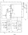
- the clamping circuit 22 is now described with reference to FIG. 4 , which shows the laser driver circuit 20'.
- the cascode current generator 40 and clamping circuit 22 are on a single integrated circuit 50, and the laser diode LD and capacitor Cvhv are external to the single integrated circuit 50.
- the laser driver circuit 20' may include multiple clamping circuits 22 coupled in parallel between the high voltage node VHV and the output node OUT.
- Each clamping circuit 22 receives its own control signal CTRL, with it being understood that the number of active clamping circuits 22 is programmable via the control signals CTRL -- when a given clamping circuit 22 has its control signal CTRL set to a logic low, that clamping circuit 22 is activated, whereas when a clamping circuit 22 has its control signal CTRL set to a logic high, that clamping circuit is deactivated.
- Each clamping circuit 22 may be identical, and therefore have identical RLC characteristics. However, in some instances, different clamping circuits 22 may have different RLC values (such as by varying the size or layout of transistor switch Tsw, etc.).
- cascode current generator 40 there may be multiple such cascode current generators 40 coupled in parallel between the output node OUT and ground.
- Cascode current generators 40 which are desired to be off have the gate of their switch SW tied to ground, while cascode current generators 40 which are desired to operate in parallel receive the same pulse trigger. Therefore, the number of active cascode current generators 40 is programmable.
- a parasitic inductance Lp1 that represents a sum of all parasitic in the series path of the capacitor Cvhv between the high voltage supply node VHV and ground (e.g., sum of the parasitic inductance of the capacitor Cvhv, the parasitic inductance of the PCB traces between the high voltage supply node VHV and ground), is illustrated as being coupled between the capacitor Cvhv and ground, but it should be understood that the inductance Lp1 represents parasitic inductances (as described) and is not a discrete component.
- the inductance Lp1 may also include a discrete inductive element, in which case it would represent the prior mentioned sum of parasitic inductances as well as the inductance of the discrete inductive element, however, for the purposes of the remainder of this disclosure, the case where the inductance Lp1 does not include a discrete inductive element is instead considered.
- a laser diode LD has its anode coupled to the high voltage supply node VHV and its cathode coupled to the output node OUT.
- a parasitic inductance Lp that represents a sum of the parasitic inductances in the series path of the laser diode LD between the output node OUT and the high voltage supply node VHV (e.g., sum of the parasitic inductance of the laser diode LD, and the parasitic inductance of the PCB traces between the output node OUT and the high voltage supply node VHV), is illustrated as being coupled between the cathode of the laser diode LD and the output node OUT, but it should be understood that the inductance Lp represents parasitic inductances (as described) and is not a discrete component.
- the inductance Lp may also include a discrete inductive element, in which case it would represent the prior mentioned sum of parasitic inductances as well as the inductance of the discrete inductive element, however, for the purposes of the remainder of this disclosure, the case where the inductance Lp does not include a discrete inductive element is instead considered.
- the cascode current generator 40 remains unchanged from that of FIG. 2 and is therefore not described again for brevity.
- the clamping circuit 22 includes a switch Tsw (which is an n-channel transistor) having a drain coupled to node N1, a source coupled to node N2, and a gate.
- a Zener diode DZ has its anode coupled to node N2 and its cathode coupled to the gate of transistor switch Tsw.
- a selection transistor Tsel (which is an n-channel transistor) has its source coupled to ground, its drain coupled to the gate of the switch Tsw, and its gate coupled to receive the control signal CTRL.
- a diode D2 has its anode coupled to node N2 and its cathode coupled to the high voltage supply node VHV.
- a diode D1 has its anode coupled to the output node OUT and its cathode coupled to node N1.
- a resistor R is coupled between nodes N1 and N2.
- the capacitor Cgd and resistor R are sized such that the gate of the switch Tsw, in response, rises higher than its source terminal (coupled to node N2). Therefore, once this gate to source voltage becomes sufficient, the switch Tsw turns on.
- CTRL remains low during operation, and therefore the transistor Tsel remains off and does not pull the gate of the switch Tsw to ground.
- the voltage between the output node OUT and the high voltage supply node VHV provides headroom to turn on diodes D1 and D2, establishing a discharge path for the voltage overshoot (from the output node OUT to the high voltage node VHV) and therefore damping the voltage overshoot (and the current undershoot).
- the active clamp path resulting from CTRL being low is turned on by the voltage overshoot on the output node OUT, thereby damping the voltage at the output node OUT.
- the damping provided by the clamp path can be programmed.
- the damping circuit 22 coupled in parallel between the high voltage node VHV and the output node.
- the programmability of the number of active clamping circuits (by setting the control signal CTRL, for each clamping circuit desired to be activated, low). This allows the proper damping for the behavior of the laser driver circuit 20' to be achieved.
- the control signal CTRL is set to high, turning on the n-channel transistor Tsel, which forces the gate of the switch Tsw to ground with a sufficiently low impedance.
- an overshoot occurring at the output node OUT and transferred to node N1 through the diode D1 is unable to be further transferred to the gate of the switch Tsw. Therefore, the switch Tsw is not turned on by an overshoot occurring at the output node OUT, and the unselected clamping circuit 22 is consequently turned off and does not offer a path to discharge overshoot at the output node OUT to VHV
- each clamping circuit 22 is identical, in some cases, the clamping circuits 22 may be different with one another in terms of sizing of Tsw, R, D1, and D2.
- a variant of the laser driver circuit 20" disclosed herein performs a pre-biasing the laser diode LD with a current (from a lasing threshold biasing circuit 45) sufficient to maintain a forward bias on the laser diode LD of just below the lasing region.
- This allows a large reduction of the turn-on time of the laser diode LD, and in turn allows an increase in the repetition rate of the laser pulses produced by the laser diode LD, as well as allowing the narrowing of the pulse width of the laser pulse output by the laser driver LD.
- the lasing threshold biasing circuit 45 is coupled in parallel with the cascode current generator 40 and has a similar structure.
- the lasing threshold biasing circuit 45 includes a current generator T3 (which is an n-channel transistor) having its source coupled to ground and its gate biased by a first bias voltage Vbias.
- a switch T2 (which is an n-channel transistor) has its source coupled to the drain of transistor current generator T3 and its gate controlled by a threshold trigger pulse from an amplifier 46.
- a cascode device (which is an n-channel transistor) T1 has its source coupled to the drain of switch T2, its gate biased by a second bias voltage Vbias,casc, and its drain coupled to the output node OUT.
- a parasitic capacitance Cp1 is illustrated as being coupled between the output node OUT and ground, and represents the total parasitic capacitance related to the lasing threshold biasing circuit 45 at the output node OUT when the lasing threshold biasing circuit 45 is activated (e.g., the output capacitance of the lasing threshold biasing circuit 45).
- An output resistance Ro1 is shown, and represents the total output resistance seen at the output node OUT (e.g., when the lasing threshold biasing circuit 45 is on, resistance Ro1 represents the output resistance of the lasing threshold biasing circuit 45).
- the threshold trigger pulse will go high a time THON before the trigger pulse goes high, turning on the switch T2 and therefore the lasing threshold biasing circuit 45, with the result being that a threshold current will be sunk from the laser diode LD, and will serve to bias the laser diode LD to just below the lasing region (shown occurring between times t0 and t1).
- the threshold trigger pulse will go low a time THOFF after the trigger pulse goes low (shown occurring between times t3 and t4), in order to remove the threshold current after the trigger pulse has completed, so as to save power. It is possible to simply have the lasing threshold biasing circuit 45 maintained on regardless of the logic state of the trigger pulse, however, this would undesirably consume power.
- Those above described laser driver circuits 20, 20', 20" may be used in any laser driving application where it is desired to drive a laser diode in the described modes.
- Example applications include a time of flight ranging system incorporating one of the above described laser driver circuits 20, 20', 20" to drive one or more laser diodes, and a LIDAR ranging system incorporating one of the above described laser driver circuits 20, 20', 20" to drive one or more laser diodes.
- prior art laser driver designs enable the generation of a pulsed drive current for a laser diode without ringing, but they fail to reduce the pulse width of the produced laser drive current sufficiently for some purposes, fail to produce a laser drive current pulse that is as high as desired for some purposes, and have a recovery time longer than desired for some purposes.
- this newly designed laser driver is sensitive to state of the pulse trigger it receives as input, which raises potential issues.
- a potential fault can originate externally (from the circuitry generating the pulse trigger) or can originate internally (due to a logic problem). If such a fault were to cause the pulse trigger to remain fixed at a logic high for longer than desired, a large DC current will flow through the laser diode, which in turn will emit a fixed (as opposed to pulsed) laser beam.
- a fixed laser beam is undesirable for a variety of reasons as it would exceed established laser power regulations, and as it would lead to self-heating of the driver circuitry in excess of what the driver circuitry is designed to withstand.
- the two potential issues with the newly designed laser driver arise from the fact that it is pulse triggered, and from the fact that the laser diode is placed so as to naturally enter a forward bias mode. These potential issues are addressed by the safety circuitry 100 of FIG. 7 , which has been developed to eliminate these potential issues.
- the safety circuitry 100 includes a p-channel transistor M2 having its source coupled to a high voltage node VHV, its drain coupled to the source of p-channel transistor M1, and its gate coupled to its drain through p-channel transistor M1 as well as to the gate of p-channel transistor M3.
- the p-channel transistor M1 has its source coupled to the drain of the p-channel transistor M2, its drain coupled to the resistor R11, and its gate coupled to the gate of the p-channel transistor M4.
- the resistor R11 is coupled between the drain of the p-channel transistor M1 and node NDnote that the laser diode 104 driven by the laser driver is coupled between VHV and node ND, and is external to the safety circuitry 100 and external to the integrated circuit 101 in which the safety circuitry 100 is contained.
- Node ND is coupled to ground in the absence of a fault internal to the integrated circuit 101.
- the p-channel transistor M3 has its source coupled to the high voltage node VHV, its drain coupled to the source of p-channel transistor M4, and its gate coupled to the gate and drain of p-channel transistor M2.
- the p-channel transistor M4 has its source coupled to the drain of the p-channel transistor M3, its drain coupled to an output node NOUT, and its gate coupled to the gate of p-channel transistor M1.
- a p-channel transistor M5 has its drain coupled to the gates of the p-channel transistors M4 and M1, its source coupled to the gates of p-channel transistors M2-M3 as well as to the drain of p-channel transistor M1, and its gate coupled directly to its drain and indirectly to its source through capacitor C11.
- a current source 103 is coupled between the drain of the p-channel transistor M5 (and the gate of the p-channel transistor M4) and ground.
- a Zener diode Dz1 has its anode coupled to the drain of the p-channel transistor M2 and source of the p-channel transistor M1, and its cathode coupled to the high voltage supply node VHV.
- a Zener diode Dz2 has its anode coupled to the gates of the p-channel transistors M2 and M3 as well as to the drain of p-channel transistor M1 and the source of p-channel transistor M5, and its cathode coupled to the high voltage supply node VHV.
- a Zener diode Dz3 has its anode coupled to the drain of the p-channel transistor M3 and source of the p-channel transistor M4, and its cathode coupled to the high voltage supply node VHV.
- a Zener diode Dz4 has its anode coupled to the current source 103, the drain of the p-channel transistor M5, and the gate of the p-channel transistor M4, and its cathode coupled to the high voltage supply node VHV
- a comparator 102 has a first input coupled to the output node NOUT, a second input coupled to receive a threshold voltage Vth, asserts or deasserts a fault flag FAULT at its output, and is powered between a supply voltage VCCA and ground.
- a p-channel transistor M6 has its source coupled to the output node NOUT, its drain coupled to ground through resistor R12, and its gate coupled to its drain.
- a Zener diode Dz5 has its anode coupled to ground and its cathode coupled to the output node NOUT.
- the p-channel transistor M2 is diode coupled because its gate is coupled to its drain through the p-channel transistor M1, which acts as a cascode device.
- the p-channel transistors M2 and M3 are in a current mirroring relationship.
- the resistors R11 and R12 are equal in resistance, and that the p-channel transistors M2 and M6 are matched. Under these conditions, assuming that the current mirror formed by p-channel transistors M2 and M3 has a 1:1 mirroring ratio, as will be explained below in detail, it is possible to shift the voltage drop Vld to be present at the input of the comparator 102. This arises from the fact that, through the p-channel transistor M6 (which is matched to M2), the gate to source voltage of p-channel transistor M2 is canceled. Stated another way, the voltage drop Vld is applied to the series circuit of p-channel transistor M2 (in diode configuration) and resistor R11.
- the current that flows through this branch is dependent on the gate to source voltage of p-channel transistor M2.
- the gate to source voltage of the p-channel transistor M2 is canceled out by the matched gate to source voltage of the p-channel transistor M6, and therefore the voltage at NOUT reflects the voltage drop Vld.
- the Zener diodes Dz1-Dz5 are clamp diodes used to protect the transistors in the safety circuit 100.
- the p-channel transistors M2, M3, M5, and M6 can be considered “standard” devices, are rated to withstand 5.5 V, and therefore their gate to source voltage and their drain to source voltage are to be lower than 5.5 V.
- the p-channel transistors M1 and M4 are considered "high voltage” devices and are to be maintained with their gate to source voltage less than 5.5 V and their drain to source voltage less than a given value that is related to the voltage class of the device (e.g., 60 V for the p-channel transistors M1 and M4).
- the Zener diode Dz2 is activated so that it will avalanche prior to the gate to source voltage of the p-channel transistors M2 and M3 exceeding a safe level, therefore clamping their gates to a safe level.
- the current generator 103, diode coupled p-channel transistor M5, and the capacitor C11 form a bias setting circuit for the cascode p-channel transistors M1 and M4.
- This parallel path includes the Zener diode Dz4, p-channel transistor M5, and resistor R11.
- the capacitor C11 acts as a filter and stabilizes the gate to source voltage of the p-channel transistor M5 against high frequency perturbations.
- the current Ibias generated by the current source 103 is sunk by the series path of the p-channel transistor M5, resistor R11, and laser diode 104.
- the voltage at the gate and source of the p-channel transistor M5 is fixed to VHV-Ibias*R11-Vld, with Vld being the forward voltage across the laser diode 104 when biased by Ibias. Therefore, by adjusting the magnitude of the bias current Ibias, a bias voltage Vbias suitable for biasing the cascode p-channel transistors M1 and M4 is generated.
- the comparator 102 receives Vrep and Vth, and if Vrep exceeds Vth, then Vld has reached an unsafe level, and the fault flag is asserted.
- a fault detection circuit 150 receives the fault flag FLAG.
- the fault detection circuit 150 includes a delay circuit 151 receiving the fault flag FLAG and outputting a delayed version of the fault flag as FAULTD.
- An AND gate 152 receives the delayed fault flag FAULTD and the fault flag FLAG, performs a logical AND operation, and drives the clock input of the flip flop 153 with the result.
- the flip flop 153 has a clock input receiving the output of the AND gate 152, a D input coupled to the supply voltage VCCA, a clear input coupled to a fault clear signal FAULT_CLR, and a Q output at which a fault output signal FAULT_OUT is generated.
- the AND gate 152 will receive a logic high from the fault flag FLAG and a logic low from the delay circuit 151 (because the fault flag FLAG has not yet had time to propagate through the delay circuit 151). Therefore, the output of the AND gate 152 will remain low until the end of the delay imposed by the delay circuit 151, at which time FAULTD will go high, and the output of the AND gate 152 will then go high, clocking the rising edge triggered clock input of the flip flop 153, and causing FAULT _OUT to go high.
- the fault output signal FAULT_OUT can be used by other components to shut down the laser driver to quench the laser drive current, after which point the fault clear signal FAULT _CLR will go high to reset the output FAULT _OUT of the flip flop 153 to low.
- the other components referred to above may take action based on the fault output signal FAULT_OUT, the fault signal FAULT itself, or a combination of the two.
- the laser driver can be shut down upon the fault signal FAULT going high, or instead upon the FAULT OUT signal going high.
- the usage of the FAULT OUT signal is particularly useful because the delay of the delay block 151 can be set to be greater than or equal to the expected period of voltage drop due to proper laser drive current pulse generation, therefore in essence filtering out the expected voltage drops.
- the threshold voltage Vth can be programmable, and also that the delay produced by the delay circuit 151 can be programmable based upon a delay select signal NSEL. This allows for fine tuning of both the voltage drop and the period of voltage drop duration that are considered to indicate a fault.
- a time of flight ranging application such as LIDAR, utilizes a laser diode driven by a laser driver that generates a pulse drive current to cause the laser diode to emit a short laser pulse in a given direction.
- the laser pulse is reflected by a possible object in the given direction
- a receiver receives and reads the reflected pulse, and by determining the elapsed time from emission of the laser pulse to receipt of the reflected pulse, the distance to the given object can be determined.
- the determination of the elapsed time from emission of the laser pulse to receipt of the reflected pulse therefore involves the determination of the instant in time at which the laser pulse was emitted.
- a capacitive coupling between the level shifter system 200 and a laser driver (here, shown as the laser driver 20 described above) is shown in FIG. 8 through which a synchronization signal indicative of the start time of the laser drive pulse is extracted from the laser driver 20 by the level shifter 200.
- This synchronization signal is used as a reference time signal by a time-to-digital-converter (TDC) 220.
- TDC time-to-digital-converter
- a TDC 220 is required to be particularly accurate for time of flight ranging operations, having a resolution on the order of tens of picoseconds.
- TDCs 220 are designed in advanced technologies where the supply voltages utilized are on the order of 1 V or less. Therefore, these TDC designs 220 are not directly compatible with signals from the laser driver 20, which utilizes a supply voltage on the order of 5 V (even neglecting the voltage at the output node OUT of the laser driver 20 that is referred to a high voltage supply VHV).
- level shifters it is known to use level shifters to move and buffer a digital signal from a higher voltage domain to a lower voltage domain (for example, from 5 V to 1 V).
- level shifters introduce a non-negligible delay between receiving the input signal to be shifted and outputting the shifted output signal. This delay can be calibrated and accounted for, however it is inherently sensitive to process, voltage, and temperature variations, which is not acceptable for a time of flight ranging system where precise timing is to be used, as this would result in an inconsistent reference starting point used by the TDC 220 to measure the time of flight of the laser pulse.
- the level shifter 200 will be described in detail below, but first the capacitive coupling itself between the laser driver 20 and level shifter system 200 is described.
- the level shifter 200 reads an AC voltage drop appearing at an appropriate node of the cascode current generator 40 of the laser driver 20. This AC voltage drop is read by the level shifter system 200 and digitized.
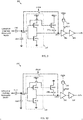
- the capacitive coupling itself can be between the input to the level shifter 200 and the output of the driver amplifier 21, and this output of the driver amplifier 21 can be moving from 0 V to VCCA (e.g., 5 V).
- the capacitive coupling can instead be between the input to the level shifter 200 and the drain of the switch transistor SW -- this has the advantage of the coupled AC voltage drop being closer in time to generation of the laser drive pulse, as opposed to the rising of the trigger pulse, which occurs prior to the generation of the laser drive pulse by the turn-on time of the transistor switch SW and the cascode current generator 40; however, this also has the disadvantage of the fact that the voltage swing on the drain of the transistor switch SW is less than 1 V, as opposed to the voltage swing of 5 V that occurs on the gate of the transistor switch SW, so the signal to read is weaker. Note that where the AC voltage drop at the output of the driver amplifier 21 is read, it is the rising edge that is read, but where the AC voltage at the drain of the switch SW is read, it is the falling edge that is read.
- the level shifter 200 shows the aforementioned capacitive coupling as capacitor C111 coupled between the laser driver 20 and the level shifter input node LSIN.
- a capacitor C222 is coupled between the level shifter input node LSIN and ground.
- a CMOS inverter 210 is formed by the p-channel transistor M12 and the n-channel transistor M11.
- the p-channel transistor M12 has its source coupled to the supply node VDDIO (which belongs to the lower voltage domain that the synchronization signal is being shifted to), its drain coupled to the level shifter output node LSOUT, and its gate coupled to the level shifter input node LSIN.
- the n-channel transistor M11 has its drain coupled to the level shifter output node LSOUT, its source coupled to ground, and its gate coupled to the level shifter input node LSIN.
- the p-channel transistor M13 is selectively coupled in parallel with the p-channel transistor M12, with its source coupled to the supply node VDDIO, its drain selectively coupled to the level shifter output node LSOUT by switch S2, and its gate coupled to the gate of the p-channel transistor M12.
- a switch S1 selectively couples the level shifter input node LSIN to the level shifter output node LSOUT.
- the switch S2 is operated based upon assertion of a control signal CTRL, while the switch S1 is operated based upon assertion of the complement CTRLB of the control signal.
- a buffer 201 has an input coupled to the level shifter output node LSOUT and an output coupled to the input of a buffer 202.
- the buffer 202 has an output providing a level shifted output signal OUTS.
- the control signal CTRL is correlated to the trigger signal from the driver amplifier 21, meaning that when the trigger signal is low, the control signal CTRL is low (so, switch S2 is open while switch S1 is closed), and when the trigger signal is high, the control signal CTRL is high (so, switch S2 is closed while switch S1 is open).
- the control signal CTRL is low, and therefore the switch S1 is closed while the switch S2 is open.
- capacitor C111 is the effective decoupling capacitor
- C222 is used to provide for capacitive partitioning so that the voltage drop that will appear at the node LSIN as a consequence of the voltage drop in the laser driver is properly attenuated to withstand the SOA of the level shifter. For example, assuming that the output of the driver 21 is switching from 0 V to 5V, if the input capacitance of the inverter 210 is negligible, the same 5 V drop will appear at the node LSIN, which is an issue if the inverter is unable to sustain this voltage.
- the capacitor C222 leads to an attenuation equal to C 111 C 111 + C 222 of the voltage drop that allows satisfaction of the SOA constraints.
- This threshold voltage is a fraction of the supply voltage VDDIO (with the fraction being related to the on resistance of the p-channel transistor M12 and the n-channel transistor M11), and when the inverter 210 is in this condition, it works as an analog amplifier as far as small signals at its input are concerned, and has a high voltage gain and wide bandwidth. This is particularly suited for reading a signal that is not a pure digital signal, such as the voltage drop from the laser driver 20 capacitively transferred to the level shifter input node LSIN.
- the inverter 210 After the switch S1 is switched off, the inverter 210 remains in its threshold condition if its input remains unchanged, but due to its high gain and large bandwidth, a slight variation at its input will lead to a switching of its output.
- the buffer 201 When the inverter 210 is in its threshold condition with its input and output equal, the buffer 201 is designed to read this voltage at the level shifter output LSOUT as a logic high (although in some cases the buffer 201 could be switched off to save power and set its output in this condition to a logic high).
- the inverter 210 When the trigger signal goes high, a delay will be present before the trigger signal is fully transferred to the level shifter input LSIN. During this delay, the inverter 210 is in its threshold condition, and due to the sensitivity in that condition, there could be multiple improper switchings of the inverter 210, which could read by the TDC 200, resulting in improper operation of the time of flight ranging system.
- switch S1 opens, the switch S2 closes, coupling the p-channel transistor M13 is parallel with the p-channel transistor M12, and therefore altering the threshold voltage of the inverter 210 to be higher than the threshold voltage was without the p-channel transistor M13 coupled in parallel.
- the inverter 210 switches its output at the level shifter output LSOUT low because the p-channel transistors M12 and M13 will turn off while transistor the M11 turns on, and this logic low will be buffered by the buffers 201 and 202 as the level shifted output signal OUTS.
- the voltage at the level shifter input LSIN will have to fall below the original threshold voltage (as opposed to the increased threshold voltage) for the inverter 210 to re-assert its output at the level shifter LSOUT as a logic high due (which here is VDDIO, which is the lower voltage domain supply) to turn the p-channel transistor M12 on and the n-channel transistor M11 off, which will be buffered by the buffers 201 and 202 as the level shifted output signal OUTS.
- VDDIO which is the lower voltage domain supply
- the role of the p-channel transistor M13 is mainly of interest to the switching off of the switch S1, as the level shifter 200 is not of great importance on the other edge -- in fact, the chief role of the level shifter 200 is to provide a clear trigger OUTS used to start the TDC 220, and it is this triggering edge that is read by the TDC, with the following edge not being influential as the TDC 220 is stopped by the receiver when a reflected laser light pulse is received.
- the inverter 210 is protected from unwanted output bouncing due to input noise, while switching its output properly and quickly as desired.
- the buffer 201 is biased by a current proportional to absolute temperature IPTAT from a current generator 203.
- the biasing of the buffer 201 with IPTAT provides for a shorter transmission delay at higher temperature and a longer transmission delay at lower temperature. Since other delays within the level shifter 200 increase with temperature, the biasing of the buffer 201 with IPTAT therefore performs a rough compensation of the global delay of the level shifter 200 against temperature variation, which is particularly useful given that the output of the inverter 210 is not purely digital in nature and has a slower slope than a purely digital signal.
- the transmitted signal switches in a purely digital fashion, and therefore the buffer 202 is not shown as being biased with IPTAT.
- the level shifted output signal OUTS output by the level shifter 200 is received by the TDC 220.
- the TDC 220 interprets this level shifted output signal OUTS as a start signal. Therefore, as soon as OUTS switches (meaning that the laser drive pulse is generated at this moment, in turn meaning that the laser diode LD has emitted a laser pulse, neglecting a slight stable delay that can be compensated for), the TDC 220 starts to count and the counting will proceed until an end point at which a reflected laser pulse is received. From this elapsed time, the distance to the object from which the laser pulse is reflected can be determined.
- the level shifter 200 of FIG. 9 is of use in the case where the capacitive coupling C111 is referred to the output of the driver amplifier 21.
- the capacitive coupling C111 is instead referred to the drain of the transistor switch SW. In that case, a negative voltage drop is to be read.
- the level shifter 200 of FIG. 9 is easily modified to handle this scenario. Therefore, with reference to FIG. 10 , the drain of the n-channel transistor M13' of the level shifter 200' is selectively coupled through the switch S2 to the node LSOUT, with the gate of M13' being coupled to LSIN and the source of M13' being coupled to ground.
- the buffer 201' will be so designed that, when the inverter 210' is in the threshold condition with the switch S1 closed, LSOUT is read as a logic low.
- the switch S1 is switched off and the switch S2 is switched on.
- the threshold of the inverter 210' is therefore lowered due to the presence of the n-channel transistor M13, confirming the status of the output of the buffer 201' (since it will read a stronger logic low at its input and avoid false switching while waiting for the negative voltage drop at LSIN that will raise the voltage at LSOUT).
- the core concept is to shift the value of the output of the inverter 210' to enforce a reset condition while waiting for the real signal to be read.
- the value is that is digitally defined at the output OUTS when the switch S2 is closed is meant. It bears repeating that in this condition with the switch S1 closed, the inverter 210' is operating in an analog mode and providing at its output the threshold voltage.
- the buffer 201' is designed in order to transfer forward clear digital information, such as by being designed to read the threshold voltage at LSOUT as a logic high or a logic low. As an alternative, the design can be to switch off and properly reset the buffer 201' itself.
Landscapes
- Physics & Mathematics (AREA)
- Condensed Matter Physics & Semiconductors (AREA)
- General Physics & Mathematics (AREA)
- Electromagnetism (AREA)
- Optics & Photonics (AREA)
- Semiconductor Lasers (AREA)
Applications Claiming Priority (1)
| Application Number | Priority Date | Filing Date | Title |
|---|---|---|---|
| US16/454,717 US10826268B1 (en) | 2019-06-27 | 2019-06-27 | Laser driver incorporating clamping circuit with freewheeling diode |
Publications (2)
| Publication Number | Publication Date |
|---|---|
| EP3758170A2 true EP3758170A2 (de) | 2020-12-30 |
| EP3758170A3 EP3758170A3 (de) | 2021-04-21 |
Family
ID=71092391
Family Applications (1)
| Application Number | Title | Priority Date | Filing Date |
|---|---|---|---|
| EP20179464.1A Withdrawn EP3758170A3 (de) | 2019-06-27 | 2020-06-11 | Lasertreiber mit klemmschaltung mit freilaufdiode |
Country Status (3)
| Country | Link |
|---|---|
| US (3) | US10826268B1 (de) |
| EP (1) | EP3758170A3 (de) |
| CN (2) | CN212875045U (de) |
Families Citing this family (13)
| Publication number | Priority date | Publication date | Assignee | Title |
|---|---|---|---|---|
| US11774561B2 (en) * | 2019-02-08 | 2023-10-03 | Luminar Technologies, Inc. | Amplifier input protection circuits |
| US10826268B1 (en) * | 2019-06-27 | 2020-11-03 | Stmicroelectronics S.R.L. | Laser driver incorporating clamping circuit with freewheeling diode |
| US11870215B2 (en) * | 2020-03-23 | 2024-01-09 | Lumentum Operations Llc | Reconfigurable laser pulse generating circuit |
| WO2021210217A1 (ja) * | 2020-04-15 | 2021-10-21 | 株式会社村田製作所 | レーザダイオード駆動回路 |
| US11757533B2 (en) * | 2021-08-13 | 2023-09-12 | Lumentum Operations Llc | Shutdown circuitry for a laser emitter |
| US11563319B1 (en) * | 2021-09-30 | 2023-01-24 | Stmicroelectronics S.R.L. | Stand-alone safety isolated area with integrated protection for supply and signal lines |
| US20230112690A1 (en) * | 2021-10-08 | 2023-04-13 | Lumentum Operations Llc | Driver circuit with a signal output |
| US11923711B2 (en) * | 2021-10-14 | 2024-03-05 | Amogy Inc. | Power management for hybrid power system |
| CN114337631B (zh) * | 2022-01-14 | 2024-09-24 | 中国电子科技集团公司第四十四研究所 | 一种硅基单光子探测器的淬灭与恢复电路及其控制方法 |
| CN115047752B (zh) * | 2022-06-09 | 2025-05-23 | 齐鲁中科电工先进电磁驱动技术研究院 | 一种半导体激光线性驱动电源的控制电路及方法 |
| EP4333305A1 (de) * | 2022-08-31 | 2024-03-06 | Nexperia B.V. | Spannungsgatetreiber für einen halbleiterbasierten transistor sowie eine leistungsschaltervorrichtung und ein entsprechendes verfahren |
| CN116169547A (zh) * | 2023-02-10 | 2023-05-26 | 武汉高思光电科技有限公司 | 一种用于mopa激光器种子源的光波形整形电路 |
| WO2025215734A1 (ja) * | 2024-04-09 | 2025-10-16 | Ntt株式会社 | Dmlドライバ |
Family Cites Families (32)
| Publication number | Priority date | Publication date | Assignee | Title |
|---|---|---|---|---|
| US5163063A (en) * | 1990-02-07 | 1992-11-10 | Copal Co., Ltd. | Semiconductor laser driving circuit |
| US5848044A (en) * | 1995-08-18 | 1998-12-08 | Kabushiki Kaisha Toshiba | Semiconductor laser driving circuit, semiconductor laser device, image recording apparatus, and optical disk apparatus |
| JP3456120B2 (ja) * | 1997-09-09 | 2003-10-14 | 三菱電機株式会社 | レーザダイオード用電源制御装置 |
| US6771133B2 (en) | 1997-10-21 | 2004-08-03 | Emhiser Research Limited | Phase-locked oscillator with improved digital integrator |
| CA2308209C (en) | 1997-10-21 | 2004-03-09 | Lloyd Lynn Lautzenhiser | Adaptive frequency-hopping oscillators |
| JP3450293B2 (ja) * | 2000-11-29 | 2003-09-22 | Necエレクトロニクス株式会社 | クロック制御回路及びクロック制御方法 |
| KR100399941B1 (ko) | 2001-06-30 | 2003-09-29 | 주식회사 하이닉스반도체 | 디디알 에스디램의 레지스터 제어 지연고정루프 |
| JP2003032104A (ja) | 2001-07-12 | 2003-01-31 | Mitsubishi Electric Corp | Dll回路とその制御方法 |
| JP2003324348A (ja) | 2002-04-30 | 2003-11-14 | Elpida Memory Inc | Dll回路 |
| US6819612B1 (en) | 2003-03-13 | 2004-11-16 | Advanced Micro Devices, Inc. | Apparatus and method for a sense amplifier circuit that samples and holds a reference voltage |
| US7372882B2 (en) * | 2004-04-28 | 2008-05-13 | Renesas Technology Corp. | Driving circuit for and semiconductor device for driving laser diode |
| US7298173B1 (en) | 2004-10-26 | 2007-11-20 | Marvell International Ltd. | Slew rate control circuit for small computer system interface (SCSI) differential driver |
| KR100776906B1 (ko) | 2006-02-16 | 2007-11-19 | 주식회사 하이닉스반도체 | 파워다운 모드 동안 주기적으로 락킹 동작을 실행하는기능을 가지는 dll 및 그 락킹 동작 방법 |
| WO2010134516A1 (ja) * | 2009-05-19 | 2010-11-25 | ローム株式会社 | 電源装置及びこれを備えた電子機器 |
| JP5326927B2 (ja) * | 2009-08-19 | 2013-10-30 | 富士電機株式会社 | レベルシフト回路 |
| JP2011066089A (ja) * | 2009-09-15 | 2011-03-31 | Ricoh Co Ltd | 半導体レーザ制御装置及び画像形成装置 |
| CN102111070B (zh) * | 2009-12-28 | 2015-09-09 | 意法半导体研发(深圳)有限公司 | 待机电流减少的调节器过电压保护电路 |
| TWI392204B (zh) * | 2010-07-06 | 2013-04-01 | Power Forest Technology Corp | 電源轉換裝置及其過電流保護方法 |
| KR101198140B1 (ko) | 2010-12-21 | 2012-11-12 | 에스케이하이닉스 주식회사 | 시프트 레지스터 및 이를 이용한 동기 회로 |
| US20140063593A1 (en) * | 2012-08-31 | 2014-03-06 | Martin Ole Berendt | Capacitor discharge pulse drive circuit with fast recovery |
| KR101382500B1 (ko) | 2013-01-18 | 2014-04-10 | 연세대학교 산학협력단 | 지연 고정 회로 및 클록 생성 방법 |
| JP6206001B2 (ja) * | 2013-08-30 | 2017-10-04 | サンケン電気株式会社 | Led駆動回路 |
| JP2015076711A (ja) | 2013-10-08 | 2015-04-20 | マイクロン テクノロジー, インク. | 半導体装置 |
| CN105337606B (zh) * | 2014-06-30 | 2018-08-31 | 意法半导体研发(深圳)有限公司 | 支持压力测试的具有栅极钳位的驱动器电路 |
| US9054485B1 (en) * | 2014-09-17 | 2015-06-09 | Hong Kong Applied Science & Technology Research Institute Company, Ltd. | Asymmetric edge compensation of both anode and cathode terminals of a vertical-cavity surface-emitting laser (VCSEL) diode |
| US9401723B2 (en) | 2014-12-12 | 2016-07-26 | Freescale Semiconductor, Inc. | XOR phase detector, phase-locked loop, and method of operating a PLL |
| US9753060B2 (en) * | 2015-08-28 | 2017-09-05 | Stmicroelectronics (Research & Development) Limited | Apparatus with device with fault detection protection |
| CN105514796B (zh) * | 2015-12-29 | 2019-01-08 | 西安交通大学 | 一种新型高重频短脉冲ld激光器及其工作过程 |
| US10574026B2 (en) * | 2017-03-23 | 2020-02-25 | Infineon Technologies Ag | Circuit and method for driving a laser diode |
| US10511142B2 (en) * | 2017-05-03 | 2019-12-17 | Analog Modules, Inc. | Pulsed laser diode drivers and methods |
| CN112098043B (zh) * | 2019-06-17 | 2022-04-15 | 光宝科技新加坡私人有限公司 | 用于检测激光发射器的故障检测电路 |
| US10826268B1 (en) * | 2019-06-27 | 2020-11-03 | Stmicroelectronics S.R.L. | Laser driver incorporating clamping circuit with freewheeling diode |
-
2019
- 2019-06-27 US US16/454,717 patent/US10826268B1/en active Active
-
2020
- 2020-06-11 EP EP20179464.1A patent/EP3758170A3/de not_active Withdrawn
- 2020-06-24 CN CN202021200058.8U patent/CN212875045U/zh active Active
- 2020-06-24 CN CN202010591912.6A patent/CN112152075A/zh active Pending
- 2020-09-21 US US17/026,495 patent/US11418007B2/en active Active
-
2022
- 2022-06-28 US US17/852,100 patent/US12413045B2/en active Active
Also Published As
| Publication number | Publication date |
|---|---|
| EP3758170A3 (de) | 2021-04-21 |
| US10826268B1 (en) | 2020-11-03 |
| CN212875045U (zh) | 2021-04-02 |
| US20220329042A1 (en) | 2022-10-13 |
| US11418007B2 (en) | 2022-08-16 |
| CN112152075A (zh) | 2020-12-29 |
| US20210006034A1 (en) | 2021-01-07 |
| US12413045B2 (en) | 2025-09-09 |
Similar Documents
| Publication | Publication Date | Title |
|---|---|---|
| US12413045B2 (en) | Laser driver incorporating clamping circuit with freewheeling diode | |
| EP3758224B1 (de) | Pvt-kompensierte verzögerungszelle für ein monostabiles monoflop | |
| US6046615A (en) | Level detection circuit | |
| US7019417B2 (en) | Power-on reset circuit with current detection | |
| US4902910A (en) | Power supply voltage level sensing circuit | |
| EP1608067B1 (de) | Rücksetzschaltung | |
| US20070001721A1 (en) | Power-on reset circuit | |
| US9270265B2 (en) | Power on reset circuit, power supply circuit, and power supply system | |
| US20070079147A1 (en) | Power up circuit with low power sleep mode operation | |
| US20100149701A1 (en) | Electrostatic discharge circuit and method | |
| EP0905605B1 (de) | Schaltung als Einschaltdetektor mit schneller Abschaltfeststellung | |
| US6515523B1 (en) | Method and apparatus for generating a power-on reset with an adjustable falling edge for power management | |
| TW202025633A (zh) | 基於GaN的高電流驅動器之故障安全停機技術 | |
| US6650155B1 (en) | Power-on reset circuit | |
| JP4191090B2 (ja) | スイッチングレギュレータ | |
| CN103391074A (zh) | 一种开关电源自锁保护电路 | |
| US6686783B1 (en) | Power-on reset system | |
| US6084446A (en) | Power on reset circuit | |
| US7221199B2 (en) | Circuit and method for generating level-triggered power up reset signal | |
| US6335646B1 (en) | Power-on reset circuit for generating a reset pulse signal upon detection of a power supply voltage | |
| Wens et al. | An integrated 10A, 2.2 ns rise-time laser-diode driver for LIDAR applications | |
| US6351109B1 (en) | Integrated circuit | |
| US7295046B2 (en) | Power down detection circuit | |
| Rigault et al. | A low-voltage sub-ns pulse integrated CMOS laser diode driver for SPAD-based time-of-flight rangefinding in mobile applications | |
| US8981734B2 (en) | Power source generation circuit and integrated circuit |
Legal Events
| Date | Code | Title | Description |
|---|---|---|---|
| PUAI | Public reference made under article 153(3) epc to a published international application that has entered the european phase |
Free format text: ORIGINAL CODE: 0009012 |
|
| STAA | Information on the status of an ep patent application or granted ep patent |
Free format text: STATUS: THE APPLICATION HAS BEEN PUBLISHED |
|
| AK | Designated contracting states |
Kind code of ref document: A2 Designated state(s): AL AT BE BG CH CY CZ DE DK EE ES FI FR GB GR HR HU IE IS IT LI LT LU LV MC MK MT NL NO PL PT RO RS SE SI SK SM TR |
|
| AX | Request for extension of the european patent |
Extension state: BA ME |
|
| PUAL | Search report despatched |
Free format text: ORIGINAL CODE: 0009013 |
|
| RIN1 | Information on inventor provided before grant (corrected) |
Inventor name: ZAMPROGNO, MARCO Inventor name: TAJFAR, ALIREZA |
|
| AK | Designated contracting states |
Kind code of ref document: A3 Designated state(s): AL AT BE BG CH CY CZ DE DK EE ES FI FR GB GR HR HU IE IS IT LI LT LU LV MC MK MT NL NO PL PT RO RS SE SI SK SM TR |
|
| AX | Request for extension of the european patent |
Extension state: BA ME |
|
| RIC1 | Information provided on ipc code assigned before grant |
Ipc: H01S 5/042 20060101AFI20210312BHEP Ipc: H01S 5/062 20060101ALI20210312BHEP Ipc: H03K 17/0814 20060101ALI20210312BHEP Ipc: H03K 17/10 20060101ALI20210312BHEP Ipc: H01S 5/068 20060101ALN20210312BHEP |
|
| STAA | Information on the status of an ep patent application or granted ep patent |
Free format text: STATUS: REQUEST FOR EXAMINATION WAS MADE |
|
| 17P | Request for examination filed |
Effective date: 20210803 |
|
| RBV | Designated contracting states (corrected) |
Designated state(s): AL AT BE BG CH CY CZ DE DK EE ES FI FR GB GR HR HU IE IS IT LI LT LU LV MC MK MT NL NO PL PT RO RS SE SI SK SM TR |
|
| STAA | Information on the status of an ep patent application or granted ep patent |
Free format text: STATUS: EXAMINATION IS IN PROGRESS |
|
| 17Q | First examination report despatched |
Effective date: 20220121 |
|
| STAA | Information on the status of an ep patent application or granted ep patent |
Free format text: STATUS: THE APPLICATION HAS BEEN WITHDRAWN |
|
| 18W | Application withdrawn |
Effective date: 20220303 |