EP3757639B1 - Optische baugruppe mit zwischenstück - Google Patents
Optische baugruppe mit zwischenstück Download PDFInfo
- Publication number
- EP3757639B1 EP3757639B1 EP20181304.5A EP20181304A EP3757639B1 EP 3757639 B1 EP3757639 B1 EP 3757639B1 EP 20181304 A EP20181304 A EP 20181304A EP 3757639 B1 EP3757639 B1 EP 3757639B1
- Authority
- EP
- European Patent Office
- Prior art keywords
- interposer
- optical
- fiber
- optical component
- contacts
- Prior art date
- Legal status (The legal status is an assumption and is not a legal conclusion. Google has not performed a legal analysis and makes no representation as to the accuracy of the status listed.)
- Active
Links
Images



Classifications
-
- G—PHYSICS
- G02—OPTICS
- G02B—OPTICAL ELEMENTS, SYSTEMS OR APPARATUS
- G02B6/00—Light guides; Structural details of arrangements comprising light guides and other optical elements, e.g. couplings
- G02B6/24—Coupling light guides
- G02B6/42—Coupling light guides with opto-electronic elements
- G02B6/4201—Packages, e.g. shape, construction, internal or external details
- G02B6/4202—Packages, e.g. shape, construction, internal or external details for coupling an active element with fibres without intermediate optical elements, e.g. fibres with plane ends, fibres with shaped ends, bundles
-
- G—PHYSICS
- G02—OPTICS
- G02B—OPTICAL ELEMENTS, SYSTEMS OR APPARATUS
- G02B6/00—Light guides; Structural details of arrangements comprising light guides and other optical elements, e.g. couplings
- G02B6/24—Coupling light guides
- G02B6/36—Mechanical coupling means
- G02B6/3628—Mechanical coupling means for mounting fibres to supporting carriers
-
- G—PHYSICS
- G02—OPTICS
- G02B—OPTICAL ELEMENTS, SYSTEMS OR APPARATUS
- G02B6/00—Light guides; Structural details of arrangements comprising light guides and other optical elements, e.g. couplings
- G02B6/24—Coupling light guides
- G02B6/42—Coupling light guides with opto-electronic elements
- G02B6/4201—Packages, e.g. shape, construction, internal or external details
- G02B6/4204—Packages, e.g. shape, construction, internal or external details the coupling comprising intermediate optical elements, e.g. lenses, holograms
- G02B6/421—Packages, e.g. shape, construction, internal or external details the coupling comprising intermediate optical elements, e.g. lenses, holograms the intermediate optical component consisting of a short length of fibre, e.g. fibre stub
-
- G—PHYSICS
- G02—OPTICS
- G02B—OPTICAL ELEMENTS, SYSTEMS OR APPARATUS
- G02B6/00—Light guides; Structural details of arrangements comprising light guides and other optical elements, e.g. couplings
- G02B6/24—Coupling light guides
- G02B6/42—Coupling light guides with opto-electronic elements
- G02B6/4201—Packages, e.g. shape, construction, internal or external details
- G02B6/4219—Mechanical fixtures for holding or positioning the elements relative to each other in the couplings; Alignment methods for the elements, e.g. measuring or observing methods especially used therefor
- G02B6/4228—Passive alignment, i.e. without a detection of the degree of coupling or the position of the elements
-
- G—PHYSICS
- G02—OPTICS
- G02B—OPTICAL ELEMENTS, SYSTEMS OR APPARATUS
- G02B6/00—Light guides; Structural details of arrangements comprising light guides and other optical elements, e.g. couplings
- G02B6/24—Coupling light guides
- G02B6/42—Coupling light guides with opto-electronic elements
- G02B6/4201—Packages, e.g. shape, construction, internal or external details
- G02B6/4219—Mechanical fixtures for holding or positioning the elements relative to each other in the couplings; Alignment methods for the elements, e.g. measuring or observing methods especially used therefor
- G02B6/4228—Passive alignment, i.e. without a detection of the degree of coupling or the position of the elements
- G02B6/423—Passive alignment, i.e. without a detection of the degree of coupling or the position of the elements using guiding surfaces for the alignment
-
- G—PHYSICS
- G02—OPTICS
- G02B—OPTICAL ELEMENTS, SYSTEMS OR APPARATUS
- G02B6/00—Light guides; Structural details of arrangements comprising light guides and other optical elements, e.g. couplings
- G02B6/24—Coupling light guides
- G02B6/42—Coupling light guides with opto-electronic elements
- G02B6/4201—Packages, e.g. shape, construction, internal or external details
- G02B6/4219—Mechanical fixtures for holding or positioning the elements relative to each other in the couplings; Alignment methods for the elements, e.g. measuring or observing methods especially used therefor
- G02B6/4236—Fixing or mounting methods of the aligned elements
- G02B6/424—Mounting of the optical light guide
-
- G—PHYSICS
- G02—OPTICS
- G02B—OPTICAL ELEMENTS, SYSTEMS OR APPARATUS
- G02B6/00—Light guides; Structural details of arrangements comprising light guides and other optical elements, e.g. couplings
- G02B6/24—Coupling light guides
- G02B6/42—Coupling light guides with opto-electronic elements
- G02B6/4201—Packages, e.g. shape, construction, internal or external details
- G02B6/4219—Mechanical fixtures for holding or positioning the elements relative to each other in the couplings; Alignment methods for the elements, e.g. measuring or observing methods especially used therefor
- G02B6/4236—Fixing or mounting methods of the aligned elements
- G02B6/4245—Mounting of the opto-electronic elements
-
- G—PHYSICS
- G02—OPTICS
- G02B—OPTICAL ELEMENTS, SYSTEMS OR APPARATUS
- G02B6/00—Light guides; Structural details of arrangements comprising light guides and other optical elements, e.g. couplings
- G02B6/24—Coupling light guides
- G02B6/42—Coupling light guides with opto-electronic elements
- G02B6/4201—Packages, e.g. shape, construction, internal or external details
- G02B6/4256—Details of housings
- G02B6/4257—Details of housings having a supporting carrier or a mounting substrate or a mounting plate
-
- G—PHYSICS
- G02—OPTICS
- G02B—OPTICAL ELEMENTS, SYSTEMS OR APPARATUS
- G02B6/00—Light guides; Structural details of arrangements comprising light guides and other optical elements, e.g. couplings
- G02B6/24—Coupling light guides
- G02B6/42—Coupling light guides with opto-electronic elements
- G02B6/4201—Packages, e.g. shape, construction, internal or external details
- G02B6/4256—Details of housings
- G02B6/426—Details of housings mounting, engaging or coupling of the package to a board, a frame or a panel
-
- G—PHYSICS
- G02—OPTICS
- G02B—OPTICAL ELEMENTS, SYSTEMS OR APPARATUS
- G02B6/00—Light guides; Structural details of arrangements comprising light guides and other optical elements, e.g. couplings
- G02B6/24—Coupling light guides
- G02B6/42—Coupling light guides with opto-electronic elements
- G02B6/4201—Packages, e.g. shape, construction, internal or external details
- G02B6/4274—Electrical aspects
- G02B6/428—Electrical aspects containing printed circuit boards [PCB]
-
- G—PHYSICS
- G02—OPTICS
- G02B—OPTICAL ELEMENTS, SYSTEMS OR APPARATUS
- G02B6/00—Light guides; Structural details of arrangements comprising light guides and other optical elements, e.g. couplings
- G02B6/24—Coupling light guides
- G02B6/42—Coupling light guides with opto-electronic elements
- G02B6/4292—Coupling light guides with opto-electronic elements the light guide being disconnectable from the opto-electronic element, e.g. mutually self aligning arrangements
-
- G—PHYSICS
- G02—OPTICS
- G02B—OPTICAL ELEMENTS, SYSTEMS OR APPARATUS
- G02B6/00—Light guides; Structural details of arrangements comprising light guides and other optical elements, e.g. couplings
- G02B6/24—Coupling light guides
- G02B6/42—Coupling light guides with opto-electronic elements
- G02B6/4201—Packages, e.g. shape, construction, internal or external details
- G02B6/4249—Packages, e.g. shape, construction, internal or external details comprising arrays of active devices and fibres
Definitions
- optical subassemblies including fiber optic interposers, and more particularly, interposers having optical features for passive alignment, direct optical coupling, and integrated electronics.
- Fiber optics are used in a wide variety of applications.
- the use of optical fibers as a medium for transmission of digital data (including voice data) is becoming increasingly more common due to the high reliability and large bandwidth available with optical transmission systems.
- Fundamental to these systems are optical subassemblies (OSA) for transmitting and/or receiving optical signals.
- OSA optical subassemblies
- the present invention fulfills this need among others.
- a prior art optical subassembly, on which the preamble of claim I is based. is disclosed in patent WO 2005/057262 .
- the subassembly includes a flexible wiring substrate with an aperture therethrough and wiring on one or both sides which is connected to: (i) a surface emitting laser on a first side of the substrate and aligned with the aperture; (ii) a driver integrated circuit; and (iii) a circuit board.
- a ferrule holder is connected to an opposite second side of the substrate and receives a ferrule containing a fiber which extends into the aperture.
- the OSA 100 comprises a fiber 104 having a first optical axis 107 and an interposer 101.
- the interposer has first and second opposing (e.g. parallel) sides 101a. 101b, and defines an alignment aperture 103 extending from the first opposing side to the second opposing side.
- the alignment aperture 103 receives the fiber and holds the fiber such that the first optical axis 107 is positioned perpendicular to the first and second opposing sides.
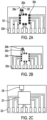
- the interposer also defines traces 102 having first, second, and third contacts, 202a, 202c, 202b (see Figs 2a-2c ).
- the first contact(s) 202a are configured for connection to the optical component, and, in one embodiment, are disposed about the perimeter 222 of the alignment aperture on the second opposing side.
- the second contact(s) 202c are configured for connection to a chip, and, in one embodiment, are disposed in the interior of the interposer.
- the third contact(s) 202b are configured for connection to a circuit board, and, in one embodiment, are disposed about the perimeter 223 of the interposer.
- the OSA also comprises at least one optical component 106 mounted to the second opposing side and electrically connected to at least a portion of the first contacts.
- the optical component has a second optical axis 108 coincident with the first optical axis 107 of the fiber.
- the fiber 104 is directly coupled optically with the at least one optical component 106.
- the OSA comprises further at least one chip 221 for operating the at least one optical component 220 (106 in in Fig. 1 ).
- the chip is mounted on either the first or second opposing side and is electrically connected to at least a portion of the second contacts.
- the interposer may comprise vias for connecting the traces between the first and second opposing sides.
- An interposer functions as a substrate for optical, opto-electrical, and electrical components and provides interconnections to optically and/or electrically interconnect the optical/opto-electrical/electrical components.
- the interposer is rigid to support the optical and electrical components, and capable of being readily machined or etched.
- the interposer comprises an insulating material to isolate electrical traces and contacts disposed thereon.
- the interposer comprises a ceramic or glass.
- the interposer may comprise a semiconductor such as silicon.
- the interposer comprises a material having essentially the same coefficient of expansion (COE) as the optical component and chip disposed thereon.
- the OSA is stable over a wide temperature range. This is particularly beneficial in applications in which sterilizing the OSA may be required such as in medical applications.
- One feature of one embodiment of the interposer is an alignment aperture to align the fiber such that the fiber's optical axis is precisely positioned in the interposer and essentially orthogonal/ perpendicular to the interposer.
- the term essentially orthogonal/ perpendicular means about 90°, not precisely 90° but for example 90° +/- 5° or so.
- the aperture is configured to hold the fiber in a precise position relative to the interposer, thereby facilitating passive alignment of the fiber with respect to the optical component. Passive alignment is generally preferred as it facilitates manufacturability (as opposed active alignment which requires energizing the optical components and then aligning optical components to optimize optical coupling).
- the alignment aperture may have different embodiments.
- the interposer is shown with a V-groove 204a for aligning the optical fiber.
- V-grooves are well-known for providing precise alignment for optical elements having a round cross-section such as an optical fiber.
- Fig. 2b an alternative embodiment is shown in which the alignment aperture is a borehole 204b.
- the V-groove and borehole are disclosed herein, it should be understood that other alignment aperture configurations can be used, including, for example, any polygon shape providing at least three points of contact with the fiber (e.g., a square aperture, hexagon aperture, etc.).
- the alignment aperture is configured as a ferrule receiver or as a receptacle to receive a plug containing the fiber.
- the first opposing side of the interposer may comprise a structure for inter-engaging mechanically with the plug.
- such a configuration may involve a ferrule receiver 118 such as that shown in Fig. 1 (and described below) and a connector comprising a ferrule from which a fiber protrudes so as to be received in the alignment aperture.
- the aperture may be configured to receive a ferrule containing a fiber.
- alignment features may be used such as alignment holes/alignment pins for ferrules (e.g. MT ferrules) or for aligning components on/under the interposer as is known to those of skill in the art in the light of this disclosure.
- direct coupling means no light bending between the optical axis of the fiber and the optical axis of the optical component. Accordingly, in a direct coupling, there are no intervening optics/reflective/refractive surfaces to change the direction of light propagation between the optical axis of the fiber and the optical axis of the optical component. In other words, unlike many conventional OSAs, the OSA of the present invention does not have reflective surfaces between the fiber and the optical component. Such an embodiment simplifies manufacturing and provides a more robust/high integrity optical path between optical components of different OSAs. For example, referring to Fig.
- a conventional interconnection 601 between a transmitter 662 and a receiver 661 is shown.
- light bending 660 is required to change the direction of light propagation from the optical components 612, 613 of the OSAs to the fiber 614.
- the optical axes 607, 608 of the optical components 612, 613 are orthogonal/perpendicular to the OSAs' circuit boards 610, 611 and fiber 614, requiring periscope optics or light bending 660 to turn the light. No such light bending is required in the interconnection 602 of the present invention.
- the transmitter 664 and the receiver 663 have optical components 622, 623 having an optical axis 609 which is essentially parallel to the circuit boards 620, 621 and coincident with the optical axis of the optical fiber 615.
- the direct coupling between the fiber in the optical component may have different embodiments.
- the optical fiber is butt coupled to the optical component as shown in Fig. 1 .
- a butt coupled interface provides a high integrity/low loss optical coupling.
- the butt coupled interface involves physically contacting the end face of the optical fiber with the optical component.
- no physical contact is made between the fiber end face and the optical component, thereby defining an airgap therebetween, as shown, for example in Fig. 1 .
- a gradient-index (GRIN) lens is disposed between the fiber end face and the optical component.
- a converging lens may be formed on the fiber end face or otherwise disposed near the end face for focusing light. Still other embodiments will be known to those of skill in the art in light of this disclosure.
- optical component may be any known or later-developed component that can be optically coupled to an optical conduit as described below.
- the optical component may be for example: (a) an optoelectric device (OED), which is an electrical device that sources, detects and/or controls light (e.g., lasers, such as vertical cavity surface emitting laser (VCSEL), double channel, planar buried heterostructure (DC-PBH), buried crescent (BC), distributed feedback (DFB), distributed bragg reflector (DBR); light-emitting diodes (LEDs), such as surface emitting LED (SLED), edge emitting LED (ELED), super luminescent diode (SLD); photodiodes, such as P Intrinsic N (PIN) and avalanche photodiode (APD); photonics processor, such as, a complementary metal oxide semiconductor (CMOS) photonic processor, for receiving optical signals, processing the signals and transmitting responsive signals, electro-optical memory, electro-optical random-access memory (EO-RAM) or electro-optical dynamic random-access memory (EO-DRAM), and electro-optical logic chips for managing optical memory (EO-logic chips)
- the optical component may be a single discrete device or it may be assembled or integrated as an array of devices.
- the optical component is a surface emitting light source.
- the surface emitting light source is a VCSEL.
- the optical component is photo sensitive.
- the photo sensitive optical component is a photodiode.
- the optical component works in conjunction with one or more electronic chips.
- a chip as used herein refers to any electronic/semiconductor chip needed to facilitate the function of the optical component.
- the chip may be a driver, or, if the optical component is a receiver, then the chip may be a transimpedance amplifier (TIA).
- TIA transimpedance amplifier
- one feature of the claimed invention is disposing both the optical component and its associated chip on the interposer. That is, rather than disposing the chip on the circuit board and electrically connecting the chip with the optical component on the interposer as is done conventionally, here, in one embodiment, the transmitter/receiver chip is disposed on the interposer in close proximity to the optical component.
- the transmitter/receiver chip is disposed on the interposer in close proximity to the optical component.
- Such a configuration has a number of important benefits. First, because the chip is in close proximity to the optical component, the traces between the chip and the optical component are very short which facilitates high speed operation by reducing impedance. Additionally, disposing the chip on the interposer eliminates the need to place it on the circuit board where space is typically limited due to the need to reduce circuit board size.
- the placement of the chip(s) on the interposer may be configured in different ways.
- the chip is disposed on the same side as the optical component, i.e. the second side.
- Such configuration has the benefit of simplicity since the optical component of the chip can be electrically connected via surface traces alone.
- the chip may be disposed on the first side of the interposer, i.e., on the opposite side of the optical component.
- Such a configuration has the benefit of utilizing space on the first opposing side of the interposer which may be important if space on the second opposing side of the interposer is limited.
- vias may be required to connect the chip on the first opposing side to its respective optical component on the second opposing side.
- the interposer comprises just a transmit or receive optical component.
- the OSA may be part of a dedicated transmitter or receiver.
- the interposer may comprise both transmit and receive optical components and the OSA may be part of a transceiver.
- the optical components may be disposed separately on the interposer, or, in one embodiment, they may be disposed in series.
- Fig. 7 shows an arrangement not forming part of the invention
- optical components in series are shown.
- the interposer 701 defines an alignment aperture through which optical fiber 704 is disposed.
- a transmitting optical component 771 is disposed adjacent the optical fiber 704.
- a second optical component for example, a receiving optical component 772
- a receiving optical component 772 may be disposed on the interposer such that its optical axis is coincident with that of the transmitting optical component 771.
- the receiving optical component 772 is behind the transmitting optical component 771, and thus, the signal received by the receiving optical component 772 passes through the transmitting optical component 771.
- the optical components be configured such that the transmitting optical component is essentially transparent to the received signal.
- Those of skill in the art will understand how to configure the transmitting optical component to be essentially transparent to the received signal in the light of this disclosure. (See, for example, Fig. 8 and associated text.)
- the receiving optical component 772 is mounted on a second interposer 773.
- the second interposer 773 comprises traces/contacts 776, 777 that electrically connect the receiving optical component 772 with the traces on the interposer 701. Separate contacts 778 are provided for electrically connecting the transmitting optical component 771 with its respective chip.
- a chip 774 is disposed on the substrate which can be configured to operate one or more of the optical components. The advantage of this configuration is that both the transmitting and receiving optical components are disposed on a single interposer and are coupled to a single fiber.
- the second planar interposer 773 may define an aperture 775 that may receive the transmitting optical component 771 which may be a surface emitting light source.
- the receiving optical component 772 may be a photo-detection chip.
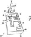
- a transmitting optical component 971 is disposed on interposer 901. Traces 991 connect the transmitting optical component 971 with its associated chip 992.
- the receiving optical component 972 is disposed over the transmitting optical component 971 and supported by the second interposer 973.
- the second interposer 973 has an orifice 975 to accommodate/receive the transmitting optical component 971.
- the second interposer 973 also has traces 990 and vias (not shown) which are configured to interface with traces 993 to connect the receiving optical component 972 to its associated chip 994.
- Third contacts 989 are disposed along the perimeter of the interposer for contact with corresponding circuit board contacts.
- the transceiver arrangement of OSA 700 simplifies installations. For example, referring to Fig. 8 , a schematic is shown in which the OSA 700 of Fig. 7 is connected to another OSA 700' via optical fiber 704. As mentioned above, such a connection does not require any additional optics/light bending to facilitate contact between optical connection between the two OSAs. Moreover, the OSAs 700, 700' facilitate bi-directional communication over a single fiber 704 according to a specific embodiment. For example, the receiving optical components 772, 772' of the OSAs 700, 700' are sensitive over a broad range, which also covers the wavelength of the transmitting optical components 771, 771'.
- the transmitting optical component 771, 771' transmit at different wavelengths, wherein the transmitting optical component 771 is transparent at the transmitting wavelength of the transmitting optical component 771', and the transmitting optical component 771' is transparent at the transmitting wavelength of the transmitting optical component 771.
- the transmitting optical component is essentially transparent to received light having a wavelength around 1310 nm.
- the transmitted signal may have a significantly shorter wavelength, e.g., around 850 nm.
- the receiving optical component 772 can receive the signal from the transmitting optical component 771', even though the transmitting optical component 771 is right in front of it because the transmitting optical component 771 is transparent to the signal from the transmitting optical component 771 (and vice versa).
- the chip is integrated with the optical component.
- the fiber's integration into the OSA of the present invention may have different arrangements. According to the invention, referring to Fig. 1 , a fiber stub is shown disposed in the borehole of the interposer. Such an embodiment facilitates manufacturing as discussed in more detail with respect to Fig. 10 .
- the interposer comprises a ferrule-receiving fixture disposed on the first opposing side to receive a connector 115.
- the ferrule-receiving fixture 118 such as a fiber alignment sleeve, has an axis coincident with the first optical axis and being configured to receive a ferrule 116 containing a terminated fiber 117 such that the terminated fiber optically couples with the fiber stub in interposer 101.
- the alignment aperture may be configured to receive a longer length of fiber or even be configured as a connector to receive a plug.
- the interposer does not have a fiber stub but instead has a longer length of a fiber that is disposed in the interposer and extends beyond the side of the interposer.
- the fiber is terminated in a ferrule, which is then disposed in the interposer.
- multiple fibers may be disposed in the interposer for a multifiber connection to the optical component(s).
- a single-fiber ferrule is shown in Fig. 1 , it should be understood that a multi-fiber ferrule, such as the MT ferrule, may be used in the interposer of the present invention according to other embodiments.
- one end of the optical fiber extends from the first opposing side 101a freely.
- one end of the optical fiber may be held in a ferrule or borehole, the other end extends freely from the interposer allowing it to be bundled/routed as need be.
- the fiber 704 extends freely from the first opposing side of the interposer, allowing the fiber to be routed or terminated as need be.
- the fiber 704 from OSA 700 is terminated in another OSA 700 as described below.
- the interposer of the present invention facilitates a variety of different OSA packaging configurations.
- the interposer of the present invention tends to be more modular, affording greater flexibility in manufacturing and packaging configurations.
- the interposer may be disposed essentially orthogonal/perpendicular to a circuit board or parallel to the circuit board, depending on the application.
- the interposer comprises contacts along the perimeter of the interposer to facilitate connection to the circuit board.
- locating the second contacts along the perimeter of the interposer is preferred as it provides a convenient connection location to the circuit board, it should be understood that other embodiments exist.
- island type connectors can be used to connect the interposer to a circuit board.
- the OSA may be embodied as a plug as or it may be integrated in a motherboard or backplane connector assembly.
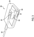
- a OSA plug 300 one embodiment of a OSA plug 300 is shown.
- the interposer 301 is disposed essentially orthogonal/ perpendicular on a printed circuit board 330.
- the fiber 333 extends from the plug such that its optical axis is essentially parallel with the printed circuit board.
- such an embodiment simplifies connections between OSAs, thereby minimizing additional components and signal losses.
- the socket 440 comprises circuit board contacts 442 for contacting corresponding contacts on a circuit board.
- Fig. 5 shows the bottom side of plug 430 and the various traces and contacts for interfacing with the socket 440. It should be understood that this plug embodiment is just one embodiment of many packages in which the interposer may be used.
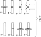
- Fig. 10 shows a method for preparing the interposer in Fig. 1 is shown.
- an insulating substrate such as a ceramic wafer is provided.
- the alignment aperture is defined in the wafer.
- the alignment aperture is a borehole which may for example be drilled through the wafer.
- a fiber stub is inserted in the borehole.
- a fritt ring is disposed between the fiber and the borehole to center the fiber in the borehole.
- the wafer is heated such that the fritt ring melts and flows into the borehole between the fiber and the wafer thereby holding the fiber in place.
- step 1006 the fiber is polished on both sides to be essentially flush with the first and second opposing sides of the wafer as shown. It should be noted that for some embodiments of the interposer, such as shown in Fig. 7 , this step 1006 could be omitted where the fiber stub of Fig. 1 is not applicable.
- step 1007 trace, contacts, and other features are deposited on the either side of the wafer as shown. It should be noted that, in this deposition step, not only are traces/contacts for the optical components/chips deposited, but also, in this embodiment, a connection for the female connector 118 is defined. Having these critical elements defined in the same deposition process is not only efficient, but also improves precision by avoiding tolerance buildup which can result from multiple deposition steps.
- step 1008 the optical components/and associated chip are disposed on the contacts on the interposer, and a ferrule-receiving structure is added to the opposite side of the interposer. It should be understood, that this is only one embodiment of preparing interposer of the present invention. Those of skill in the art will appreciate many variations are possible within the scope of the claims.
Landscapes
- Physics & Mathematics (AREA)
- General Physics & Mathematics (AREA)
- Optics & Photonics (AREA)
- Optical Couplings Of Light Guides (AREA)
- Engineering & Computer Science (AREA)
- Microelectronics & Electronic Packaging (AREA)
Claims (7)
- Optische Baugruppe (100), die Folgendes umfasst:einen Interposer (101) mit einer ersten (101a) und einer gegenüberliegenden zweiten (101b) Seite, der eine Ausrichtungsöffnung (103) definiert, die sich von der ersten gegenüberliegenden Seite (101a) zu der genannten zweiten gegenüberliegenden Seite (101b) erstreckt, wobei der genannte Interposer (101) Leiterbahnen (102) mit ersten, zweiten und dritten Kontakten (202a, 202c, 202b) definiert, wobei die genannten ersten Kontakte (202a) für eine elektrische Verbindung mit mindestens einer optischen Komponente (106, 220) konfiguriert sind, die genannten zweiten Kontakte (202c) für eine elektrische Verbindung mit mindestens einem Chip (221) konfiguriert sind und die genannten dritten Kontakte (202b) für eine elektrische Verbindung mit einer Leiterplatte konfiguriert sind;mindestens eine Faser (104), die zumindest teilweise in der genannten Ausrichtungsöffnung (103) angeordnet ist und eine erste optische Achse (107) aufweist, wobei die genannte Faser (104) so gehalten wird, dass die genannte erste optische Achse (107) im Wesentlichen orthogonal zu der genannten ersten (101a) und gegenüberliegenden zweiten (101b) Seite positioniert ist;wobei die genannte mindestens eine optische Komponente (106, 220) auf der genannten zweiten gegenüberliegenden Seite (101b) montiert und elektrisch mit mindestens einem Teil der genannten ersten Kontakte (202a) verbunden ist, wobei die genannte mindestens eine optische Komponente (106, 220) eine zweite optische Achse (108) aufweist, die mit der genannten ersten optischen Achse (107) zusammenfällt;wobei der genannte mindestens eine Chip (221) zum Betreiben der genannten mindestens einen optischen Komponente (106, 220) dient, wobei der genannte mindestens eine Chip (221) auf der genannten ersten (101a) oder gegenüberliegenden zweiten (101b) Seite montiert und elektrisch mit mindestens einem Teil der genannten zweiten Kontakte (202c) verbunden ist; undwobei die genannte Leiterplatte zum Aufnehmen des genannten Interposers (101) konfiguriert ist, so dass der Interposer (101) im Wesentlichen orthogonal zu der genannten Leiterplatte ist, wobei die genannte Leiterplatte elektrisch mit mindestens einem Teil der genannten dritten Kontakte (202b) verbunden ist, wobei die genannte Faser (104) ein Faserstummel (104) ist;dadurch gekennzeichnet, dass:(i) der genannte Interposer (101) starr und planar ist;(ii) der genannte Faserstummel (104) poliert ist, so dass er bündig mit der ersten (101a) und gegenüberliegenden zweiten (101b) Seite ist.
- Optische Baugruppe (100) nach Anspruch 1, die ferner eine auf der ersten gegenüberliegenden Seite (101a) angeordnete Adernendhülsenaufnahmestruktur (118) umfasst, wobei die genannte Adernendhülsenaufnahmestruktur (118) eine Achse aufweist, die mit der genannten ersten optischen Achse (107) zusammenfällt, und zum Aufnehmen einer Adernendhülse (116) konfiguriert ist, die eine abgeschlossene Faser (117) enthält, so dass die genannte abgeschlossene Faser (117) optisch mit dem genannten Faserstummel (104) gekoppelt ist.
- Optische Baugruppe (100) nach Anspruch 1, die ferner eine auf der genannten ersten gegenüberliegenden Seite (101a) angeordnete Adernendhülsenaufnahmestruktur (118) umfasst, wobei die genannte Adernendhülsenaufnahmestruktur (118) eine Achse aufweist, die mit der genannten ersten Achse (107) zusammenfällt, und zum Aufnehmen einer Adernendhülse (116) konfiguriert ist, die eine Faser (117) enthält, so dass die genannte Faser (117) optisch mit der genannten optischen Komponente (106, 220) gekoppelt ist.
- Optische Baugruppe (100) nach einem vorherigen Anspruch, wobei die genannten ersten Kontakte (202a) um einen Umfang (222) der genannten Ausrichtungsöffnung (103) auf der genannten zweiten gegenüberliegenden Seite (101b) angeordnet sind, die genannten zweiten Kontakte (202c) in einem inneren Abschnitt der genannten ersten (101a) oder gegenüberliegenden zweiten (101b) Seite des genannten Interposers (101) angeordnet sind und die genannten dritten Kontakte (202b) um einen Umfang (223) des Interposers (101) angeordnet sind.
- Optische Baugruppe (100) nach einem vorherigen Anspruch, wobei der genannte mindestens eine Chip (221) auf der genannten zweiten gegenüberliegenden Seite (101b) des genannten Interposers (101) montiert ist.
- Optische Baugruppe (100) nach Anspruch 1, wobei die genannte mindestens eine optische Komponente (106, 220) eine oberflächenemittierende Lichtquelle umfasst.
- Optische Baugruppe (100) nach einem vorherigen Anspruch, wobei die genannte mindestens eine optische Komponente (106, 220) einen VCSEL und/oder eine Fotodiode umfasst, wobei der genannte mindestens eine Chip ein Treiber und/oder ein Transimpedanzverstärker (TIA) ist.
Applications Claiming Priority (1)
| Application Number | Priority Date | Filing Date | Title |
|---|---|---|---|
| US16/450,189 US12474529B2 (en) | 2019-06-24 | 2019-06-24 | Interposer |
Publications (2)
| Publication Number | Publication Date |
|---|---|
| EP3757639A1 EP3757639A1 (de) | 2020-12-30 |
| EP3757639B1 true EP3757639B1 (de) | 2025-04-30 |
Family
ID=71120031
Family Applications (1)
| Application Number | Title | Priority Date | Filing Date |
|---|---|---|---|
| EP20181304.5A Active EP3757639B1 (de) | 2019-06-24 | 2020-06-22 | Optische baugruppe mit zwischenstück |
Country Status (3)
| Country | Link |
|---|---|
| US (1) | US12474529B2 (de) |
| EP (1) | EP3757639B1 (de) |
| CN (1) | CN112130262B (de) |
Families Citing this family (2)
| Publication number | Priority date | Publication date | Assignee | Title |
|---|---|---|---|---|
| US10852489B1 (en) | 2019-06-24 | 2020-12-01 | Te Connectivity Nederland B.V. | High density optical transceiver assembly |
| US12282137B2 (en) | 2020-12-23 | 2025-04-22 | Te Connectivity Solutions Gmbh | Light source for an optical sensor |
Family Cites Families (17)
| Publication number | Priority date | Publication date | Assignee | Title |
|---|---|---|---|---|
| US5631987A (en) | 1995-06-07 | 1997-05-20 | Reliaspeed, Inc. | Low cost, mode-field matched, high performance laser transmitter optical subassembly |
| US6522673B1 (en) | 1999-12-22 | 2003-02-18 | New Focus, Inc. | Method and apparatus for optical transmission |
| JP3795877B2 (ja) * | 2003-07-28 | 2006-07-12 | 株式会社東芝 | 光半導体モジュール及びその製造方法 |
| JPWO2005057262A1 (ja) | 2003-12-15 | 2007-08-23 | 日本電気株式会社 | 光モジュールおよびその製造方法 |
| DE602004032008D1 (de) | 2003-12-26 | 2011-05-12 | Toshiba Kk | Optische Halbleitermodul und Verfahren zu dessen Herstellung |
| JP2005257879A (ja) * | 2004-03-10 | 2005-09-22 | Fujitsu Ltd | 光モジュール及びその製造方法並びに保護部材及び電気配線付き保護部材 |
| WO2008090833A1 (ja) * | 2007-01-26 | 2008-07-31 | Japan Aviation Electronics Industry, Limited | 光電変換接続装置 |
| JP4957503B2 (ja) | 2007-10-16 | 2012-06-20 | 住友電気工業株式会社 | 光モジュールおよび光モジュールの製造方法 |
| US9151917B2 (en) * | 2008-09-30 | 2015-10-06 | Ytel Photonics Inc. | Optical interconnection apparatus and method |
| JP5493744B2 (ja) * | 2009-11-12 | 2014-05-14 | 富士通株式会社 | 光電気混載基板、および、光電気混載基板の製造方法 |
| US9551844B2 (en) * | 2011-01-11 | 2017-01-24 | Hewlett Packard Enterprise Development Lp | Passive optical alignment |
| US8961039B2 (en) * | 2012-06-21 | 2015-02-24 | Hirose Electric Co., Ltd. | Optical-electric conversion connector |
| US9497860B2 (en) | 2012-11-07 | 2016-11-15 | Lattice Semiconductor Corporation | Methods and Apparatuses to provide an electro-optical alignment |
| JP6300442B2 (ja) | 2013-01-18 | 2018-03-28 | オリンパス株式会社 | 光伝送モジュールおよび撮像装置 |
| EP3125008A1 (de) | 2015-07-29 | 2017-02-01 | CCS Technology Inc. | Verfahren zur herstellung optoelektronischer module |
| WO2018150512A1 (ja) * | 2017-02-16 | 2018-08-23 | オリンパス株式会社 | 光モジュール、内視鏡、および、光モジュールの製造方法 |
| JP2019056719A (ja) | 2017-09-19 | 2019-04-11 | 住友電気工業株式会社 | 光通信モジュールの製造方法、光通信モジュールの製造装置、及び光通信モジュール |
-
2019
- 2019-06-24 US US16/450,189 patent/US12474529B2/en active Active
-
2020
- 2020-06-22 EP EP20181304.5A patent/EP3757639B1/de active Active
- 2020-06-23 CN CN202010580105.4A patent/CN112130262B/zh active Active
Also Published As
| Publication number | Publication date |
|---|---|
| EP3757639A1 (de) | 2020-12-30 |
| US12474529B2 (en) | 2025-11-18 |
| CN112130262A (zh) | 2020-12-25 |
| US20200400901A1 (en) | 2020-12-24 |
| CN112130262B (zh) | 2023-07-21 |
Similar Documents
| Publication | Publication Date | Title |
|---|---|---|
| EP3596520B1 (de) | Anordnungen anlösbarer optischer verbinder und optischer chips | |
| US8412052B2 (en) | Surface mount (SMT) connector for VCSEL and photodiode arrays | |
| US10128954B2 (en) | Integrated transceiver with lightpipe coupler | |
| US7539367B2 (en) | Optical system connection structure, optical component, and optical communication module | |
| US7399125B1 (en) | Lens array with integrated folding mirror | |
| EP3165953B1 (de) | Photoelektrisches umwandlungsmodul | |
| CN104246566B (zh) | 多通道收发器 | |
| US9178620B2 (en) | Optical interface for bidirectional communications | |
| US9791640B2 (en) | Interposer with separable interface | |
| CN110582712A (zh) | 具有集成透镜的光纤模块 | |
| GB2386695A (en) | Connecting optic fibre to optoelectronic device with optical waveguide | |
| US8821040B2 (en) | Interposer | |
| CN113625399A (zh) | 一种光模块 | |
| EP3757639A1 (de) | Zwischenstück | |
| US6491446B1 (en) | Passive self-alignment technique for array laser transmitters and receivers for fiber optic applications | |
| US9651749B1 (en) | Interposer with opaque substrate | |
| US9473239B2 (en) | Systems and methods for aligning an optical interface assembly with an integrated circuit | |
| US8636426B2 (en) | Photoelectric conversion system with optical transceive module | |
| US12204149B2 (en) | Interposer with feedback | |
| US9039302B2 (en) | Interposer | |
| KR100398045B1 (ko) | 광 송수신 모듈 | |
| US20150212267A1 (en) | Optical Assembly |
Legal Events
| Date | Code | Title | Description |
|---|---|---|---|
| PUAI | Public reference made under article 153(3) epc to a published international application that has entered the european phase |
Free format text: ORIGINAL CODE: 0009012 |
|
| STAA | Information on the status of an ep patent application or granted ep patent |
Free format text: STATUS: THE APPLICATION HAS BEEN PUBLISHED |
|
| AK | Designated contracting states |
Kind code of ref document: A1 Designated state(s): AL AT BE BG CH CY CZ DE DK EE ES FI FR GB GR HR HU IE IS IT LI LT LU LV MC MK MT NL NO PL PT RO RS SE SI SK SM TR |
|
| AX | Request for extension of the european patent |
Extension state: BA ME |
|
| STAA | Information on the status of an ep patent application or granted ep patent |
Free format text: STATUS: REQUEST FOR EXAMINATION WAS MADE |
|
| 17P | Request for examination filed |
Effective date: 20210628 |
|
| RBV | Designated contracting states (corrected) |
Designated state(s): AL AT BE BG CH CY CZ DE DK EE ES FI FR GB GR HR HU IE IS IT LI LT LU LV MC MK MT NL NO PL PT RO RS SE SI SK SM TR |
|
| STAA | Information on the status of an ep patent application or granted ep patent |
Free format text: STATUS: EXAMINATION IS IN PROGRESS |
|
| 17Q | First examination report despatched |
Effective date: 20220517 |
|
| GRAP | Despatch of communication of intention to grant a patent |
Free format text: ORIGINAL CODE: EPIDOSNIGR1 |
|
| STAA | Information on the status of an ep patent application or granted ep patent |
Free format text: STATUS: GRANT OF PATENT IS INTENDED |
|
| INTG | Intention to grant announced |
Effective date: 20250114 |
|
| GRAS | Grant fee paid |
Free format text: ORIGINAL CODE: EPIDOSNIGR3 |
|
| GRAA | (expected) grant |
Free format text: ORIGINAL CODE: 0009210 |
|
| STAA | Information on the status of an ep patent application or granted ep patent |
Free format text: STATUS: THE PATENT HAS BEEN GRANTED |
|
| AK | Designated contracting states |
Kind code of ref document: B1 Designated state(s): AL AT BE BG CH CY CZ DE DK EE ES FI FR GB GR HR HU IE IS IT LI LT LU LV MC MK MT NL NO PL PT RO RS SE SI SK SM TR |
|
| REG | Reference to a national code |
Ref country code: CH Ref legal event code: EP Ref country code: GB Ref legal event code: FG4D |
|
| REG | Reference to a national code |
Ref country code: DE Ref legal event code: R096 Ref document number: 602020050300 Country of ref document: DE |
|
| REG | Reference to a national code |
Ref country code: IE Ref legal event code: FG4D |
|
| PGFP | Annual fee paid to national office [announced via postgrant information from national office to epo] |
Ref country code: DE Payment date: 20250429 Year of fee payment: 6 |
|
| PGFP | Annual fee paid to national office [announced via postgrant information from national office to epo] |
Ref country code: GB Payment date: 20250501 Year of fee payment: 6 |
|
| PGFP | Annual fee paid to national office [announced via postgrant information from national office to epo] |
Ref country code: FR Payment date: 20250508 Year of fee payment: 6 |
|
| REG | Reference to a national code |
Ref country code: NL Ref legal event code: MP Effective date: 20250430 |
|
| REG | Reference to a national code |
Ref country code: AT Ref legal event code: MK05 Ref document number: 1790524 Country of ref document: AT Kind code of ref document: T Effective date: 20250430 |
|
| PG25 | Lapsed in a contracting state [announced via postgrant information from national office to epo] |
Ref country code: FI Free format text: LAPSE BECAUSE OF FAILURE TO SUBMIT A TRANSLATION OF THE DESCRIPTION OR TO PAY THE FEE WITHIN THE PRESCRIBED TIME-LIMIT Effective date: 20250430 Ref country code: PT Free format text: LAPSE BECAUSE OF FAILURE TO SUBMIT A TRANSLATION OF THE DESCRIPTION OR TO PAY THE FEE WITHIN THE PRESCRIBED TIME-LIMIT Effective date: 20250901 Ref country code: ES Free format text: LAPSE BECAUSE OF FAILURE TO SUBMIT A TRANSLATION OF THE DESCRIPTION OR TO PAY THE FEE WITHIN THE PRESCRIBED TIME-LIMIT Effective date: 20250430 |
|
| REG | Reference to a national code |
Ref country code: LT Ref legal event code: MG9D |
|
| PG25 | Lapsed in a contracting state [announced via postgrant information from national office to epo] |
Ref country code: NO Free format text: LAPSE BECAUSE OF FAILURE TO SUBMIT A TRANSLATION OF THE DESCRIPTION OR TO PAY THE FEE WITHIN THE PRESCRIBED TIME-LIMIT Effective date: 20250730 Ref country code: GR Free format text: LAPSE BECAUSE OF FAILURE TO SUBMIT A TRANSLATION OF THE DESCRIPTION OR TO PAY THE FEE WITHIN THE PRESCRIBED TIME-LIMIT Effective date: 20250731 |
|
| PG25 | Lapsed in a contracting state [announced via postgrant information from national office to epo] |
Ref country code: PL Free format text: LAPSE BECAUSE OF FAILURE TO SUBMIT A TRANSLATION OF THE DESCRIPTION OR TO PAY THE FEE WITHIN THE PRESCRIBED TIME-LIMIT Effective date: 20250430 Ref country code: NL Free format text: LAPSE BECAUSE OF FAILURE TO SUBMIT A TRANSLATION OF THE DESCRIPTION OR TO PAY THE FEE WITHIN THE PRESCRIBED TIME-LIMIT Effective date: 20250430 |
|
| PG25 | Lapsed in a contracting state [announced via postgrant information from national office to epo] |
Ref country code: BG Free format text: LAPSE BECAUSE OF FAILURE TO SUBMIT A TRANSLATION OF THE DESCRIPTION OR TO PAY THE FEE WITHIN THE PRESCRIBED TIME-LIMIT Effective date: 20250430 |
|
| PG25 | Lapsed in a contracting state [announced via postgrant information from national office to epo] |
Ref country code: HR Free format text: LAPSE BECAUSE OF FAILURE TO SUBMIT A TRANSLATION OF THE DESCRIPTION OR TO PAY THE FEE WITHIN THE PRESCRIBED TIME-LIMIT Effective date: 20250430 |
|
| PG25 | Lapsed in a contracting state [announced via postgrant information from national office to epo] |
Ref country code: AT Free format text: LAPSE BECAUSE OF FAILURE TO SUBMIT A TRANSLATION OF THE DESCRIPTION OR TO PAY THE FEE WITHIN THE PRESCRIBED TIME-LIMIT Effective date: 20250430 |
|
| PG25 | Lapsed in a contracting state [announced via postgrant information from national office to epo] |
Ref country code: RS Free format text: LAPSE BECAUSE OF FAILURE TO SUBMIT A TRANSLATION OF THE DESCRIPTION OR TO PAY THE FEE WITHIN THE PRESCRIBED TIME-LIMIT Effective date: 20250731 |
|
| PG25 | Lapsed in a contracting state [announced via postgrant information from national office to epo] |
Ref country code: IS Free format text: LAPSE BECAUSE OF FAILURE TO SUBMIT A TRANSLATION OF THE DESCRIPTION OR TO PAY THE FEE WITHIN THE PRESCRIBED TIME-LIMIT Effective date: 20250830 |
|
| PG25 | Lapsed in a contracting state [announced via postgrant information from national office to epo] |
Ref country code: LV Free format text: LAPSE BECAUSE OF FAILURE TO SUBMIT A TRANSLATION OF THE DESCRIPTION OR TO PAY THE FEE WITHIN THE PRESCRIBED TIME-LIMIT Effective date: 20250430 |
|
| PG25 | Lapsed in a contracting state [announced via postgrant information from national office to epo] |
Ref country code: DK Free format text: LAPSE BECAUSE OF FAILURE TO SUBMIT A TRANSLATION OF THE DESCRIPTION OR TO PAY THE FEE WITHIN THE PRESCRIBED TIME-LIMIT Effective date: 20250430 Ref country code: SM Free format text: LAPSE BECAUSE OF FAILURE TO SUBMIT A TRANSLATION OF THE DESCRIPTION OR TO PAY THE FEE WITHIN THE PRESCRIBED TIME-LIMIT Effective date: 20250430 |
|
| PG25 | Lapsed in a contracting state [announced via postgrant information from national office to epo] |
Ref country code: CZ Free format text: LAPSE BECAUSE OF FAILURE TO SUBMIT A TRANSLATION OF THE DESCRIPTION OR TO PAY THE FEE WITHIN THE PRESCRIBED TIME-LIMIT Effective date: 20250430 |
|
| PG25 | Lapsed in a contracting state [announced via postgrant information from national office to epo] |
Ref country code: EE Free format text: LAPSE BECAUSE OF FAILURE TO SUBMIT A TRANSLATION OF THE DESCRIPTION OR TO PAY THE FEE WITHIN THE PRESCRIBED TIME-LIMIT Effective date: 20250430 |
|
| PG25 | Lapsed in a contracting state [announced via postgrant information from national office to epo] |
Ref country code: RO Free format text: LAPSE BECAUSE OF FAILURE TO SUBMIT A TRANSLATION OF THE DESCRIPTION OR TO PAY THE FEE WITHIN THE PRESCRIBED TIME-LIMIT Effective date: 20250430 Ref country code: SK Free format text: LAPSE BECAUSE OF FAILURE TO SUBMIT A TRANSLATION OF THE DESCRIPTION OR TO PAY THE FEE WITHIN THE PRESCRIBED TIME-LIMIT Effective date: 20250430 |
|
| REG | Reference to a national code |
Ref country code: CH Ref legal event code: H13 Free format text: ST27 STATUS EVENT CODE: U-0-0-H10-H13 (AS PROVIDED BY THE NATIONAL OFFICE) Effective date: 20260127 |
|
| PG25 | Lapsed in a contracting state [announced via postgrant information from national office to epo] |
Ref country code: IT Free format text: LAPSE BECAUSE OF FAILURE TO SUBMIT A TRANSLATION OF THE DESCRIPTION OR TO PAY THE FEE WITHIN THE PRESCRIBED TIME-LIMIT Effective date: 20250430 |
|
| PG25 | Lapsed in a contracting state [announced via postgrant information from national office to epo] |
Ref country code: MC Free format text: LAPSE BECAUSE OF FAILURE TO SUBMIT A TRANSLATION OF THE DESCRIPTION OR TO PAY THE FEE WITHIN THE PRESCRIBED TIME-LIMIT Effective date: 20250430 |
|
| REG | Reference to a national code |
Ref country code: DE Ref legal event code: R097 Ref document number: 602020050300 Country of ref document: DE |
|
| PG25 | Lapsed in a contracting state [announced via postgrant information from national office to epo] |
Ref country code: LU Free format text: LAPSE BECAUSE OF NON-PAYMENT OF DUE FEES Effective date: 20250622 |
|
| REG | Reference to a national code |
Ref country code: BE Ref legal event code: MM Effective date: 20250630 |
|
| PLBE | No opposition filed within time limit |
Free format text: ORIGINAL CODE: 0009261 |
|
| STAA | Information on the status of an ep patent application or granted ep patent |
Free format text: STATUS: NO OPPOSITION FILED WITHIN TIME LIMIT |
|
| REG | Reference to a national code |
Ref country code: CH Ref legal event code: L10 Free format text: ST27 STATUS EVENT CODE: U-0-0-L10-L00 (AS PROVIDED BY THE NATIONAL OFFICE) Effective date: 20260311 |
|
| 26N | No opposition filed |
Effective date: 20260202 |
|
| PG25 | Lapsed in a contracting state [announced via postgrant information from national office to epo] |
Ref country code: IE Free format text: LAPSE BECAUSE OF NON-PAYMENT OF DUE FEES Effective date: 20250622 |
|
| PG25 | Lapsed in a contracting state [announced via postgrant information from national office to epo] |
Ref country code: BE Free format text: LAPSE BECAUSE OF NON-PAYMENT OF DUE FEES Effective date: 20250630 |
|
| PG25 | Lapsed in a contracting state [announced via postgrant information from national office to epo] |
Ref country code: CH Free format text: LAPSE BECAUSE OF NON-PAYMENT OF DUE FEES Effective date: 20250630 |