EP3751024A1 - Kunststoffhalbleitermaterial und verfahren zu seiner herstellung - Google Patents
Kunststoffhalbleitermaterial und verfahren zu seiner herstellung Download PDFInfo
- Publication number
- EP3751024A1 EP3751024A1 EP18905300.2A EP18905300A EP3751024A1 EP 3751024 A1 EP3751024 A1 EP 3751024A1 EP 18905300 A EP18905300 A EP 18905300A EP 3751024 A1 EP3751024 A1 EP 3751024A1
- Authority
- EP
- European Patent Office
- Prior art keywords
- semiconductor material
- inorganic semiconductor
- preparation
- sintering
- semiconductor
- Prior art date
- Legal status (The legal status is an assumption and is not a legal conclusion. Google has not performed a legal analysis and makes no representation as to the accuracy of the status listed.)
- Pending
Links
Images


Classifications
-
- C—CHEMISTRY; METALLURGY
- C30—CRYSTAL GROWTH
- C30B—SINGLE-CRYSTAL GROWTH; UNIDIRECTIONAL SOLIDIFICATION OF EUTECTIC MATERIAL OR UNIDIRECTIONAL DEMIXING OF EUTECTOID MATERIAL; REFINING BY ZONE-MELTING OF MATERIAL; PRODUCTION OF A HOMOGENEOUS POLYCRYSTALLINE MATERIAL WITH DEFINED STRUCTURE; SINGLE CRYSTALS OR HOMOGENEOUS POLYCRYSTALLINE MATERIAL WITH DEFINED STRUCTURE; AFTER-TREATMENT OF SINGLE CRYSTALS OR A HOMOGENEOUS POLYCRYSTALLINE MATERIAL WITH DEFINED STRUCTURE; APPARATUS THEREFOR
- C30B11/00—Single-crystal growth by normal freezing or freezing under temperature gradient, e.g. Bridgman-Stockbarger method
- C30B11/02—Single-crystal growth by normal freezing or freezing under temperature gradient, e.g. Bridgman-Stockbarger method without using solvents
-
- C—CHEMISTRY; METALLURGY
- C04—CEMENTS; CONCRETE; ARTIFICIAL STONE; CERAMICS; REFRACTORIES
- C04B—LIME, MAGNESIA; SLAG; CEMENTS; COMPOSITIONS THEREOF, e.g. MORTARS, CONCRETE OR LIKE BUILDING MATERIALS; ARTIFICIAL STONE; CERAMICS; REFRACTORIES; TREATMENT OF NATURAL STONE
- C04B35/00—Shaped ceramic products characterised by their composition; Ceramics compositions; Processing powders of inorganic compounds preparatory to the manufacturing of ceramic products
- C04B35/622—Forming processes; Processing powders of inorganic compounds preparatory to the manufacturing of ceramic products
- C04B35/64—Burning or sintering processes
- C04B35/645—Pressure sintering
-
- C—CHEMISTRY; METALLURGY
- C01—INORGANIC CHEMISTRY
- C01B—NON-METALLIC ELEMENTS; COMPOUNDS THEREOF; METALLOIDS OR COMPOUNDS THEREOF NOT COVERED BY SUBCLASS C01C
- C01B19/00—Selenium; Tellurium; Compounds thereof
- C01B19/002—Compounds containing, besides selenium or tellurium, more than one other element, with -O- and -OH not being considered as anions
-
- C—CHEMISTRY; METALLURGY
- C04—CEMENTS; CONCRETE; ARTIFICIAL STONE; CERAMICS; REFRACTORIES
- C04B—LIME, MAGNESIA; SLAG; CEMENTS; COMPOSITIONS THEREOF, e.g. MORTARS, CONCRETE OR LIKE BUILDING MATERIALS; ARTIFICIAL STONE; CERAMICS; REFRACTORIES; TREATMENT OF NATURAL STONE
- C04B35/00—Shaped ceramic products characterised by their composition; Ceramics compositions; Processing powders of inorganic compounds preparatory to the manufacturing of ceramic products
- C04B35/515—Shaped ceramic products characterised by their composition; Ceramics compositions; Processing powders of inorganic compounds preparatory to the manufacturing of ceramic products based on non-oxide ceramics
- C04B35/547—Shaped ceramic products characterised by their composition; Ceramics compositions; Processing powders of inorganic compounds preparatory to the manufacturing of ceramic products based on non-oxide ceramics based on sulfides or selenides or tellurides
-
- C—CHEMISTRY; METALLURGY
- C04—CEMENTS; CONCRETE; ARTIFICIAL STONE; CERAMICS; REFRACTORIES
- C04B—LIME, MAGNESIA; SLAG; CEMENTS; COMPOSITIONS THEREOF, e.g. MORTARS, CONCRETE OR LIKE BUILDING MATERIALS; ARTIFICIAL STONE; CERAMICS; REFRACTORIES; TREATMENT OF NATURAL STONE
- C04B35/00—Shaped ceramic products characterised by their composition; Ceramics compositions; Processing powders of inorganic compounds preparatory to the manufacturing of ceramic products
- C04B35/622—Forming processes; Processing powders of inorganic compounds preparatory to the manufacturing of ceramic products
- C04B35/626—Preparing or treating the powders individually or as batches ; preparing or treating macroscopic reinforcing agents for ceramic products, e.g. fibres; mechanical aspects section B
- C04B35/62605—Treating the starting powders individually or as mixtures
- C04B35/6261—Milling
- C04B35/6262—Milling of calcined, sintered clinker or ceramics
-
- C—CHEMISTRY; METALLURGY
- C04—CEMENTS; CONCRETE; ARTIFICIAL STONE; CERAMICS; REFRACTORIES
- C04B—LIME, MAGNESIA; SLAG; CEMENTS; COMPOSITIONS THEREOF, e.g. MORTARS, CONCRETE OR LIKE BUILDING MATERIALS; ARTIFICIAL STONE; CERAMICS; REFRACTORIES; TREATMENT OF NATURAL STONE
- C04B35/00—Shaped ceramic products characterised by their composition; Ceramics compositions; Processing powders of inorganic compounds preparatory to the manufacturing of ceramic products
- C04B35/622—Forming processes; Processing powders of inorganic compounds preparatory to the manufacturing of ceramic products
- C04B35/653—Processes involving a melting step
-
- C—CHEMISTRY; METALLURGY
- C30—CRYSTAL GROWTH
- C30B—SINGLE-CRYSTAL GROWTH; UNIDIRECTIONAL SOLIDIFICATION OF EUTECTIC MATERIAL OR UNIDIRECTIONAL DEMIXING OF EUTECTOID MATERIAL; REFINING BY ZONE-MELTING OF MATERIAL; PRODUCTION OF A HOMOGENEOUS POLYCRYSTALLINE MATERIAL WITH DEFINED STRUCTURE; SINGLE CRYSTALS OR HOMOGENEOUS POLYCRYSTALLINE MATERIAL WITH DEFINED STRUCTURE; AFTER-TREATMENT OF SINGLE CRYSTALS OR A HOMOGENEOUS POLYCRYSTALLINE MATERIAL WITH DEFINED STRUCTURE; APPARATUS THEREFOR
- C30B11/00—Single-crystal growth by normal freezing or freezing under temperature gradient, e.g. Bridgman-Stockbarger method
- C30B11/04—Single-crystal growth by normal freezing or freezing under temperature gradient, e.g. Bridgman-Stockbarger method adding crystallising materials or reactants forming it in situ to the melt
- C30B11/08—Single-crystal growth by normal freezing or freezing under temperature gradient, e.g. Bridgman-Stockbarger method adding crystallising materials or reactants forming it in situ to the melt every component of the crystal composition being added during the crystallisation
- C30B11/10—Solid or liquid components, e.g. Verneuil method
-
- C—CHEMISTRY; METALLURGY
- C30—CRYSTAL GROWTH
- C30B—SINGLE-CRYSTAL GROWTH; UNIDIRECTIONAL SOLIDIFICATION OF EUTECTIC MATERIAL OR UNIDIRECTIONAL DEMIXING OF EUTECTOID MATERIAL; REFINING BY ZONE-MELTING OF MATERIAL; PRODUCTION OF A HOMOGENEOUS POLYCRYSTALLINE MATERIAL WITH DEFINED STRUCTURE; SINGLE CRYSTALS OR HOMOGENEOUS POLYCRYSTALLINE MATERIAL WITH DEFINED STRUCTURE; AFTER-TREATMENT OF SINGLE CRYSTALS OR A HOMOGENEOUS POLYCRYSTALLINE MATERIAL WITH DEFINED STRUCTURE; APPARATUS THEREFOR
- C30B28/00—Production of homogeneous polycrystalline material with defined structure
- C30B28/02—Production of homogeneous polycrystalline material with defined structure directly from the solid state
-
- C—CHEMISTRY; METALLURGY
- C30—CRYSTAL GROWTH
- C30B—SINGLE-CRYSTAL GROWTH; UNIDIRECTIONAL SOLIDIFICATION OF EUTECTIC MATERIAL OR UNIDIRECTIONAL DEMIXING OF EUTECTOID MATERIAL; REFINING BY ZONE-MELTING OF MATERIAL; PRODUCTION OF A HOMOGENEOUS POLYCRYSTALLINE MATERIAL WITH DEFINED STRUCTURE; SINGLE CRYSTALS OR HOMOGENEOUS POLYCRYSTALLINE MATERIAL WITH DEFINED STRUCTURE; AFTER-TREATMENT OF SINGLE CRYSTALS OR A HOMOGENEOUS POLYCRYSTALLINE MATERIAL WITH DEFINED STRUCTURE; APPARATUS THEREFOR
- C30B29/00—Single crystals or homogeneous polycrystalline material with defined structure characterised by the material or by their shape
- C30B29/10—Inorganic compounds or compositions
- C30B29/12—Halides
-
- C—CHEMISTRY; METALLURGY
- C30—CRYSTAL GROWTH
- C30B—SINGLE-CRYSTAL GROWTH; UNIDIRECTIONAL SOLIDIFICATION OF EUTECTIC MATERIAL OR UNIDIRECTIONAL DEMIXING OF EUTECTOID MATERIAL; REFINING BY ZONE-MELTING OF MATERIAL; PRODUCTION OF A HOMOGENEOUS POLYCRYSTALLINE MATERIAL WITH DEFINED STRUCTURE; SINGLE CRYSTALS OR HOMOGENEOUS POLYCRYSTALLINE MATERIAL WITH DEFINED STRUCTURE; AFTER-TREATMENT OF SINGLE CRYSTALS OR A HOMOGENEOUS POLYCRYSTALLINE MATERIAL WITH DEFINED STRUCTURE; APPARATUS THEREFOR
- C30B29/00—Single crystals or homogeneous polycrystalline material with defined structure characterised by the material or by their shape
- C30B29/10—Inorganic compounds or compositions
- C30B29/46—Sulfur-, selenium- or tellurium-containing compounds
-
- C—CHEMISTRY; METALLURGY
- C30—CRYSTAL GROWTH
- C30B—SINGLE-CRYSTAL GROWTH; UNIDIRECTIONAL SOLIDIFICATION OF EUTECTIC MATERIAL OR UNIDIRECTIONAL DEMIXING OF EUTECTOID MATERIAL; REFINING BY ZONE-MELTING OF MATERIAL; PRODUCTION OF A HOMOGENEOUS POLYCRYSTALLINE MATERIAL WITH DEFINED STRUCTURE; SINGLE CRYSTALS OR HOMOGENEOUS POLYCRYSTALLINE MATERIAL WITH DEFINED STRUCTURE; AFTER-TREATMENT OF SINGLE CRYSTALS OR A HOMOGENEOUS POLYCRYSTALLINE MATERIAL WITH DEFINED STRUCTURE; APPARATUS THEREFOR
- C30B33/00—After-treatment of single crystals or homogeneous polycrystalline material with defined structure
- C30B33/02—Heat treatment
-
- H—ELECTRICITY
- H10—SEMICONDUCTOR DEVICES; ELECTRIC SOLID-STATE DEVICES NOT OTHERWISE PROVIDED FOR
- H10D—INORGANIC ELECTRIC SEMICONDUCTOR DEVICES
- H10D62/00—Semiconductor bodies, or regions thereof, of devices having potential barriers
- H10D62/80—Semiconductor bodies, or regions thereof, of devices having potential barriers characterised by the materials
-
- H—ELECTRICITY
- H10—SEMICONDUCTOR DEVICES; ELECTRIC SOLID-STATE DEVICES NOT OTHERWISE PROVIDED FOR
- H10N—ELECTRIC SOLID-STATE DEVICES NOT OTHERWISE PROVIDED FOR
- H10N10/00—Thermoelectric devices comprising a junction of dissimilar materials, i.e. devices exhibiting Seebeck or Peltier effects
- H10N10/80—Constructional details
- H10N10/85—Thermoelectric active materials
- H10N10/851—Thermoelectric active materials comprising inorganic compositions
- H10N10/852—Thermoelectric active materials comprising inorganic compositions comprising tellurium, selenium or sulfur
-
- C—CHEMISTRY; METALLURGY
- C01—INORGANIC CHEMISTRY
- C01P—INDEXING SCHEME RELATING TO STRUCTURAL AND PHYSICAL ASPECTS OF SOLID INORGANIC COMPOUNDS
- C01P2002/00—Crystal-structural characteristics
- C01P2002/60—Compounds characterised by their crystallite size
-
- C—CHEMISTRY; METALLURGY
- C01—INORGANIC CHEMISTRY
- C01P—INDEXING SCHEME RELATING TO STRUCTURAL AND PHYSICAL ASPECTS OF SOLID INORGANIC COMPOUNDS
- C01P2004/00—Particle morphology
- C01P2004/01—Particle morphology depicted by an image
- C01P2004/03—Particle morphology depicted by an image obtained by SEM
-
- C—CHEMISTRY; METALLURGY
- C01—INORGANIC CHEMISTRY
- C01P—INDEXING SCHEME RELATING TO STRUCTURAL AND PHYSICAL ASPECTS OF SOLID INORGANIC COMPOUNDS
- C01P2006/00—Physical properties of inorganic compounds
- C01P2006/40—Electric properties
-
- C—CHEMISTRY; METALLURGY
- C04—CEMENTS; CONCRETE; ARTIFICIAL STONE; CERAMICS; REFRACTORIES
- C04B—LIME, MAGNESIA; SLAG; CEMENTS; COMPOSITIONS THEREOF, e.g. MORTARS, CONCRETE OR LIKE BUILDING MATERIALS; ARTIFICIAL STONE; CERAMICS; REFRACTORIES; TREATMENT OF NATURAL STONE
- C04B2235/00—Aspects relating to ceramic starting mixtures or sintered ceramic products
- C04B2235/02—Composition of constituents of the starting material or of secondary phases of the final product
- C04B2235/30—Constituents and secondary phases not being of a fibrous nature
- C04B2235/40—Metallic constituents or additives not added as binding phase
- C04B2235/404—Refractory metals
-
- C—CHEMISTRY; METALLURGY
- C04—CEMENTS; CONCRETE; ARTIFICIAL STONE; CERAMICS; REFRACTORIES
- C04B—LIME, MAGNESIA; SLAG; CEMENTS; COMPOSITIONS THEREOF, e.g. MORTARS, CONCRETE OR LIKE BUILDING MATERIALS; ARTIFICIAL STONE; CERAMICS; REFRACTORIES; TREATMENT OF NATURAL STONE
- C04B2235/00—Aspects relating to ceramic starting mixtures or sintered ceramic products
- C04B2235/02—Composition of constituents of the starting material or of secondary phases of the final product
- C04B2235/30—Constituents and secondary phases not being of a fibrous nature
- C04B2235/40—Metallic constituents or additives not added as binding phase
- C04B2235/405—Iron group metals
-
- C—CHEMISTRY; METALLURGY
- C04—CEMENTS; CONCRETE; ARTIFICIAL STONE; CERAMICS; REFRACTORIES
- C04B—LIME, MAGNESIA; SLAG; CEMENTS; COMPOSITIONS THEREOF, e.g. MORTARS, CONCRETE OR LIKE BUILDING MATERIALS; ARTIFICIAL STONE; CERAMICS; REFRACTORIES; TREATMENT OF NATURAL STONE
- C04B2235/00—Aspects relating to ceramic starting mixtures or sintered ceramic products
- C04B2235/02—Composition of constituents of the starting material or of secondary phases of the final product
- C04B2235/30—Constituents and secondary phases not being of a fibrous nature
- C04B2235/40—Metallic constituents or additives not added as binding phase
- C04B2235/407—Copper
-
- C—CHEMISTRY; METALLURGY
- C04—CEMENTS; CONCRETE; ARTIFICIAL STONE; CERAMICS; REFRACTORIES
- C04B—LIME, MAGNESIA; SLAG; CEMENTS; COMPOSITIONS THEREOF, e.g. MORTARS, CONCRETE OR LIKE BUILDING MATERIALS; ARTIFICIAL STONE; CERAMICS; REFRACTORIES; TREATMENT OF NATURAL STONE
- C04B2235/00—Aspects relating to ceramic starting mixtures or sintered ceramic products
- C04B2235/02—Composition of constituents of the starting material or of secondary phases of the final product
- C04B2235/30—Constituents and secondary phases not being of a fibrous nature
- C04B2235/40—Metallic constituents or additives not added as binding phase
- C04B2235/408—Noble metals
-
- C—CHEMISTRY; METALLURGY
- C04—CEMENTS; CONCRETE; ARTIFICIAL STONE; CERAMICS; REFRACTORIES
- C04B—LIME, MAGNESIA; SLAG; CEMENTS; COMPOSITIONS THEREOF, e.g. MORTARS, CONCRETE OR LIKE BUILDING MATERIALS; ARTIFICIAL STONE; CERAMICS; REFRACTORIES; TREATMENT OF NATURAL STONE
- C04B2235/00—Aspects relating to ceramic starting mixtures or sintered ceramic products
- C04B2235/02—Composition of constituents of the starting material or of secondary phases of the final product
- C04B2235/30—Constituents and secondary phases not being of a fibrous nature
- C04B2235/42—Non metallic elements added as constituents or additives, e.g. sulfur, phosphor, selenium or tellurium
-
- C—CHEMISTRY; METALLURGY
- C04—CEMENTS; CONCRETE; ARTIFICIAL STONE; CERAMICS; REFRACTORIES
- C04B—LIME, MAGNESIA; SLAG; CEMENTS; COMPOSITIONS THEREOF, e.g. MORTARS, CONCRETE OR LIKE BUILDING MATERIALS; ARTIFICIAL STONE; CERAMICS; REFRACTORIES; TREATMENT OF NATURAL STONE
- C04B2235/00—Aspects relating to ceramic starting mixtures or sintered ceramic products
- C04B2235/02—Composition of constituents of the starting material or of secondary phases of the final product
- C04B2235/30—Constituents and secondary phases not being of a fibrous nature
- C04B2235/44—Metal salt constituents or additives chosen for the nature of the anions, e.g. hydrides or acetylacetonate
- C04B2235/444—Halide containing anions, e.g. bromide, iodate, chlorite
-
- C—CHEMISTRY; METALLURGY
- C04—CEMENTS; CONCRETE; ARTIFICIAL STONE; CERAMICS; REFRACTORIES
- C04B—LIME, MAGNESIA; SLAG; CEMENTS; COMPOSITIONS THEREOF, e.g. MORTARS, CONCRETE OR LIKE BUILDING MATERIALS; ARTIFICIAL STONE; CERAMICS; REFRACTORIES; TREATMENT OF NATURAL STONE
- C04B2235/00—Aspects relating to ceramic starting mixtures or sintered ceramic products
- C04B2235/65—Aspects relating to heat treatments of ceramic bodies such as green ceramics or pre-sintered ceramics, e.g. burning, sintering or melting processes
- C04B2235/656—Aspects relating to heat treatments of ceramic bodies such as green ceramics or pre-sintered ceramics, e.g. burning, sintering or melting processes characterised by specific heating conditions during heat treatment
- C04B2235/6562—Heating rate
-
- C—CHEMISTRY; METALLURGY
- C04—CEMENTS; CONCRETE; ARTIFICIAL STONE; CERAMICS; REFRACTORIES
- C04B—LIME, MAGNESIA; SLAG; CEMENTS; COMPOSITIONS THEREOF, e.g. MORTARS, CONCRETE OR LIKE BUILDING MATERIALS; ARTIFICIAL STONE; CERAMICS; REFRACTORIES; TREATMENT OF NATURAL STONE
- C04B2235/00—Aspects relating to ceramic starting mixtures or sintered ceramic products
- C04B2235/65—Aspects relating to heat treatments of ceramic bodies such as green ceramics or pre-sintered ceramics, e.g. burning, sintering or melting processes
- C04B2235/656—Aspects relating to heat treatments of ceramic bodies such as green ceramics or pre-sintered ceramics, e.g. burning, sintering or melting processes characterised by specific heating conditions during heat treatment
- C04B2235/6567—Treatment time
-
- C—CHEMISTRY; METALLURGY
- C04—CEMENTS; CONCRETE; ARTIFICIAL STONE; CERAMICS; REFRACTORIES
- C04B—LIME, MAGNESIA; SLAG; CEMENTS; COMPOSITIONS THEREOF, e.g. MORTARS, CONCRETE OR LIKE BUILDING MATERIALS; ARTIFICIAL STONE; CERAMICS; REFRACTORIES; TREATMENT OF NATURAL STONE
- C04B2235/00—Aspects relating to ceramic starting mixtures or sintered ceramic products
- C04B2235/65—Aspects relating to heat treatments of ceramic bodies such as green ceramics or pre-sintered ceramics, e.g. burning, sintering or melting processes
- C04B2235/66—Specific sintering techniques, e.g. centrifugal sintering
- C04B2235/661—Multi-step sintering
- C04B2235/662—Annealing after sintering
-
- C—CHEMISTRY; METALLURGY
- C04—CEMENTS; CONCRETE; ARTIFICIAL STONE; CERAMICS; REFRACTORIES
- C04B—LIME, MAGNESIA; SLAG; CEMENTS; COMPOSITIONS THEREOF, e.g. MORTARS, CONCRETE OR LIKE BUILDING MATERIALS; ARTIFICIAL STONE; CERAMICS; REFRACTORIES; TREATMENT OF NATURAL STONE
- C04B2235/00—Aspects relating to ceramic starting mixtures or sintered ceramic products
- C04B2235/65—Aspects relating to heat treatments of ceramic bodies such as green ceramics or pre-sintered ceramics, e.g. burning, sintering or melting processes
- C04B2235/66—Specific sintering techniques, e.g. centrifugal sintering
- C04B2235/666—Applying a current during sintering, e.g. plasma sintering [SPS], electrical resistance heating or pulse electric current sintering [PECS]
-
- C—CHEMISTRY; METALLURGY
- C04—CEMENTS; CONCRETE; ARTIFICIAL STONE; CERAMICS; REFRACTORIES
- C04B—LIME, MAGNESIA; SLAG; CEMENTS; COMPOSITIONS THEREOF, e.g. MORTARS, CONCRETE OR LIKE BUILDING MATERIALS; ARTIFICIAL STONE; CERAMICS; REFRACTORIES; TREATMENT OF NATURAL STONE
- C04B2235/00—Aspects relating to ceramic starting mixtures or sintered ceramic products
- C04B2235/70—Aspects relating to sintered or melt-casted ceramic products
- C04B2235/74—Physical characteristics
- C04B2235/77—Density
-
- C—CHEMISTRY; METALLURGY
- C04—CEMENTS; CONCRETE; ARTIFICIAL STONE; CERAMICS; REFRACTORIES
- C04B—LIME, MAGNESIA; SLAG; CEMENTS; COMPOSITIONS THEREOF, e.g. MORTARS, CONCRETE OR LIKE BUILDING MATERIALS; ARTIFICIAL STONE; CERAMICS; REFRACTORIES; TREATMENT OF NATURAL STONE
- C04B2235/00—Aspects relating to ceramic starting mixtures or sintered ceramic products
- C04B2235/70—Aspects relating to sintered or melt-casted ceramic products
- C04B2235/74—Physical characteristics
- C04B2235/78—Grain sizes and shapes, product microstructures, e.g. acicular grains, equiaxed grains, platelet-structures
- C04B2235/786—Micrometer sized grains, i.e. from 1 to 100 micron
-
- C—CHEMISTRY; METALLURGY
- C04—CEMENTS; CONCRETE; ARTIFICIAL STONE; CERAMICS; REFRACTORIES
- C04B—LIME, MAGNESIA; SLAG; CEMENTS; COMPOSITIONS THEREOF, e.g. MORTARS, CONCRETE OR LIKE BUILDING MATERIALS; ARTIFICIAL STONE; CERAMICS; REFRACTORIES; TREATMENT OF NATURAL STONE
- C04B2235/00—Aspects relating to ceramic starting mixtures or sintered ceramic products
- C04B2235/70—Aspects relating to sintered or melt-casted ceramic products
- C04B2235/74—Physical characteristics
- C04B2235/79—Non-stoichiometric products, e.g. perovskites (ABO3) with an A/B-ratio other than 1
Definitions
- the present application relates to a plastic inorganic semiconductor material and a preparation method thereof, which belongs to the field of semiconductor materials.
- the first technical route is to use organic semiconductors as a base material. Because organic matter itself has a certain deformability, chip elements made by N-type and P-type regulation of organic matter can also withstand a certain amount of deformation.
- inorganic semiconductor materials are prepared ( Münzenrieder N, Salvatore G A, Kinkeldei T, et al. InGaZnO TFTs on a flexible membrane transferred to a curved surface with a radius of 2 mm[J]. 2013:165-166 .).
- the dimensions of inorganic semiconductor materials are within a certain range, they can withstand a certain degree of bending deformation, and thus can be combined with a deformable organic polymer substrate to prepare a semiconductor chip that can bear a certain deformation.
- This method can maintain the high performance of inorganic semiconductor devices, but it will lead to chip peeling and performance degradation after multiple deformations due to the combination of inorganic and organic materials.
- due to the limitation of technological conditions and fabrication capacities such inorganic/organic composite flexible semiconductor devices have high fabrication costs and low yields.
- a purpose of the present application is to provide a material that can not only withstand a certain deformation, similar to organic materials, but also has excellent semiconductor performance with adjustable electrical properties, thereby enabling the preparation of high-performance flexible semiconductor devices.
- the present application provides an inorganic semiconductor material having plastic deformability with adjustable electrical properties, comprising an argentite-based compound represented by the following formula (I): Ag 2- ⁇ X ⁇ S 1- ⁇ Y ⁇ (I), in which,
- the inorganic semiconductor material of the present application has great plastic deformability under compression, tension, and bending stress, and thus can meet the requirements of flexible electronic devices for deformable semiconductor materials, and can provide a novel solution for the new generation of flexible semiconductor devices.
- a band gap of the inorganic semiconductor material may be adjusted within the range of 0.5 to 1.5 eV, and an electrical conductivity thereof may be adjusted within the range of 0.001 to 250,000 S/m.
- the inorganic semiconductor material may withstand a tensile deformation of 3% or more, a bending deformation of 13% or more, and a compression deformation of 30% or more.
- 0 ⁇ ⁇ ⁇ 0.05, and 0 ⁇ ⁇ ⁇ 0.05 Preferably, 0 ⁇ ⁇ ⁇ 0.05, and 0 ⁇ ⁇ ⁇ 0.05.
- the semiconductor material may be a single crystal.
- the semiconductor material may be a polycrystal.
- the grain size of the polycrystal may range from 1 ⁇ m to 5 mm and the density thereof may be 95% or more.
- the present application provides a preparation method of the inorganic semiconductor material mentioned above, comprising the steps of:
- the present application has a simple process, is easy to control, and has a good industrialization prospect.
- the preparation method further comprises an annealing step after cooling.
- the annealing temperature is 400 to 650 °C and the annealing time is 1 to 300 hours.
- the sintering is spark plasma sintering or hot-pressed sintering.
- the sintering temperature is 100 to 400 °C
- the pressure is 10 to 100 MPa
- the sintering time is 5 to 120 minutes.
- the crystal growth process by Bridgman-Stockbarge method comprises the steps of:
- the plastic semiconductor material of the present application can not only withstand a certain deformation, similar to organic materials, but also has excellent semiconductor performance with adjustable electrical properties, thereby enabling the preparation of high-performance flexible semiconductor devices.
- the inventors of the present application have developed a novel inorganic semiconductor material with plastic deformability and a preparation method thereof after extensive and in-depth research, thus improving the deformation resistance and fragile characteristics of semiconductor materials.
- the present disclosure provides a semiconductor material, the host in which is an argentite semiconductor compound.
- the semiconductor material comprises an argentite-based compound represented by the following formula (I): Ag 2- ⁇ X ⁇ S 1- ⁇ Y ⁇ (I).
- X may be one or more selected from the group consisting of Cu, Au, Fe, Co, Ni, Zn, Ti, and V.
- Y may be one or more selected from the group consisting of N, P, As, Sb, Se, Te, O, Br, CI, I, and F.
- the band gap, electrical conductivity and other properties of the material may be adjusted by doping of X and Y.
- Ag 2 S has a plastic property, and such a unique deformable plastic property, together with its adjustable electrical property over a wide range, allow Ag 2 S to be used to prepare a variety of deformable semiconductor devices.
- X may be one or more selected from the group consisting of Cu, Zn, and Ni.
- Y may be one or more selected from the group consisting of Se, Te, Cl, Br, and I.
- 0 ⁇ ⁇ ⁇ 0.5 Preferably, 0 ⁇ ⁇ ⁇ 0.5. In a preferred example, 0 ⁇ ⁇ ⁇ 0.05. In another preferred example, 0.1 ⁇ ⁇ ⁇ 0. 5.
- 0 ⁇ ⁇ ⁇ 0.5 In the formula, 0 ⁇ ⁇ ⁇ 0.5. Preferably, 0 ⁇ ⁇ ⁇ 0.5. In a preferred example, 0 ⁇ ⁇ ⁇ 0.05. In another preferred example, 0.1 ⁇ ⁇ ⁇ 0.5.
- 0 ⁇ ⁇ ⁇ 0.05, and 0 ⁇ ⁇ ⁇ 0.05 In a preferred example, 0 ⁇ ⁇ ⁇ 0.05, and 0 ⁇ ⁇ ⁇ 0.05.
- formula (I) is Ag 2 S.
- 0.1 ⁇ ⁇ ⁇ 0.5, and 0.1 ⁇ ⁇ ⁇ 0.5 are preferred examples.
- formula (I) is Ag 1.8 Cu 0.2 S 0.9 Se 0.1 .
- the crystal structure of the semiconductor material presents a lamellar-like structure.
- doping atoms X and Y can be evenly distributed in the corresponding lattice locations, without affecting the lamellar-like structure of the argentite itself.
- the semiconductor material may be a single-crystalline material (also referred to as "single crystal").
- single-crystalline material means that the whole material is composed of a single grain.
- the semiconductor material may be a polycrystalline material (also referred to as "polycrystal").
- polycrystalline material means that the whole material is composed of many small crystals arranged disorderly.
- the grain size of the polycrystalline material ranges from 1 ⁇ m to 5 mm.
- the density of the polycrystalline material may be 95% or more, even 98% or more.
- the polycrystalline material has a simpler preparation process, while maintaining good plasticity and other properties.
- the semiconductor material may be an N-type doped semiconductor material or a P-type doped semiconductor material.
- the content of other impurities in the semiconductor material is 1 at% or less.
- the band gap of the semiconductor material may be adjusted within the range of 0.5 to 1.5 eV, preferably within the range of 0.5 to 1.2 eV.
- the electrical conductivity of the semiconductor material may be adjusted within the range of 0.001 to 250,000 S/m, preferably within the range of 0.01 to 1,000 S/m, more preferably within the range of 1 to 1,000 S/m.
- the semiconductor material has a good plasticity. For example, it can withstand a tensile deformation of 3% or more, a bending deformation of 13% or more, even 20% or more, and a compression deformation of 30% or more.
- the semiconductor disclosed herein can withstand certain deformation, similar to organic materials, and has excellent semiconductor performance with adjustable electrical properties, thereby enabling the preparation of high-performance flexible semiconductor devices.
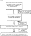
- FIG. 7 shows a process flow diagram of preparing a polycrystalline plastic semiconductor material in Embodiment 1.
- raw materials are made into a block solid (such as a crystal rod) with evenly distributed components through a solid phase reaction.
- the raw materials used may be elementary substances of the constituent elements of formula (I), or compound composed of the elements.
- the raw materials are preferably high-purity materials, for example, have a purity of 99% or more.
- the ratio between raw materials may be in accordance with the stoichiometric ratio of formula (I).
- the raw materials are mixed and melted to give a molten mixture.
- the raw materials are mixed and then heated to 850 to 1,200 °C to melt.
- the raw materials can be kept at this temperature for 1 to 20 hours.
- the heating rate may be 0.5 to 3 °C/min.
- the raw materials are encapsulated and melted in a sealed container.
- the sealed container may be a quartz tube.
- the sealed container may be a common tube or a crystal growing tube with a pointed tip at its top.
- a quartz tube is used as the sealing container, a uniform carbon film can be coated on the inner wall of the quartz tube, or the raw materials can be placed into a graphite crucible and then encapsulated in the quartz tube, so as to prevent the reaction between the raw materials and the quartz tube.
- the melting may be performed in an inert atmosphere or in vacuum.
- the vacuum degree may be 0.1 to 40,000 Pa, preferably 0.1 to 1,000 Pa.
- the obtained molten mixture is cooled to form a block solid.
- the cooling method may be quenching in quenching medium, or slow cooling.
- the quenching medium may be air, water, saturated brine, oil, or liquid nitrogen.
- the block solid may be further annealed to make the doping components more uniform and improve the crystallinity of the material.
- the annealing temperature may be 400 to 650 °C, preferably 550 to 650 °C.
- the annealing time may be 1 to 300 hours, preferably 200 to 300 hours.
- the block solid is ground into powder.
- the size of the powder may be 1 to 100 ⁇ m.
- the powder is sintered to give a polycrystalline material.
- the sintering method may be pressure sintering, such as spark plasma sintering or hot-pressed sintering.
- the sintering temperature may be 100 to 400 °C, preferably 200 to 300 °C.
- the pressure applied may be 10 to 100 MPa, preferably 30 to 60 MPa.
- the sintering time may be 5 to 120 minutes, preferably 5 to 30 minutes.
- FIG. 8 shows a process flow diagram of preparing a single-crystalline plastic semiconductor material in Embodiment 2.
- raw materials are made into a block solid (such as a crystal rod) with evenly distributed components through a solid phase reaction.
- a block solid such as a crystal rod
- This step can be taken in the same way as Embodiment 1 and will not be repeated here.
- the block solid is made into a single-crystalline material.
- the block solid is subjected to a crystal growth process by a Bridgman-Stockbarger method, to give a single-crystalline semiconductor material.
- the obtained block solid is placed in a crystal growing tube with a pointed tip at its top (see FIG. 9 ).
- the crystal growing tube for example, may be a quartz tube.
- a crystal growing tube with a pointed tip at its top can be used as a sealed container in the preparation of the block solid (i.e., a crystal growing tube with a pointed tip is used before the initial melting). This eliminates the need to take out the block solid and place it in a crystal growing tube.
- a crystal growing tube filled with the block solid is placed in a constant temperature zone of a crystal growing furnace.
- the temperature of the constant temperature zone may range from 830 °C to 950 °C.
- the temperature gradient of the constant temperature zone may be 1 °C/cm to 100 °C/cm, preferably 1 °C/cm to 5 °C/cm.
- the crucible lowering rate may be 0.1 mm/h to 10 mm/h, preferably 0.1 mm/h to 1 mm/h.
- the size of the obtained single-crystalline semiconductor material may be 1 mm to 50 mm in diameter and 5 mm to 50 mm in height.
- the disclosed semiconductor material can be used to prepare flexible semiconductor devices, such as flexible semiconductor chips, etc.
- the disclosed preparation method is controllable and suitable for batch industrial production.
- the raw materials were encapsulated into a quartz tube with a carbon film deposited on the inner wall.
- the quartz tube was sealed with argon plasma flame while being vacuumized, and was filled with a small amount of Ar gas as a protective atmosphere.
- the mixed raw materials were heated at a rate of 3 °C/min to 900 °C, and melted thereat for 12 hours. Quenching was carried out after the melting, and the quenching medium is brine.
- a crystal rod obtained by quenching, together with the quartz tube, were annealed at 500 °C for 100 hours.
- the crystal rod was grinded into fine powder, and subjected to spark plasma sintering to give an Ag 1.8 Cu 0.2 S 0.9 Se 0.1 polycrystalline block material.
- the sintering temperature was 400 °C, the holding time was 2 minutes, and the pressure was 30 MPa.
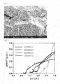
- FIG. 1 shows a cross section FESEM (field emission scanning electron microscopy) photograph of Ag 2- ⁇ X ⁇ S 1- ⁇ Y ⁇ material obtained from example 1, and it can be seen that the grain size is 5 to 10 ⁇ m.
- a spectral absorption test showed that the band gap was 0.73 eV (see FIG. 2 ).
- a test by a four-probe method showed that the electrical conductivity at room temperature was 20 S/m (see FIG. 3 ).
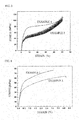
- Samples with a size of 4 mm ⁇ 4 mm ⁇ 30 mm were tested using a three-point bending method, and the bending stress-strain curve showed that the maximum bending deformation reached 15%.
- the size of samples for a compression deformation test at room temperature was 20 mm in diameter ⁇ 20 mm in height, and the maximum compression deformation reached 40%.
- the samples for an extension test were dumbbell-shaped, and had a neck size of 5 mm in diameter ⁇ 30 mm, and the maximum elongation reached 3.2% (see FIG. 4 to FIG. 6 ).
- a spectral absorption test showed that the band gap was 0.90 eV (see FIG. 2 ).
- a test showed that the electrical conductivity of the material obtained from example 2 at room temperature was 0.15 S/m.
- a test of mechanical properties at room temperature showed that the material had a good plasticity. The maximum bending deformation reached 20%, the compression deformation reached 50%, and the tensile elongation reached 4.2% (see FIG. 4 to FIG. 6 ).
- the crystal rod was grinded into fine powder, and subjected to spark plasma sintering to give an Ag 1.9 Zn 0.1 S 0.85 I 0.15 polycrystalline block material.
- the sintering temperature was 380 °C, the holding time was 5 minutes, and the pressure was 40 MPa.
- a spectral absorption test showed that the band gap was 0.78 eV (see FIG. 2 ).
- a test by a drainage method showed that the density of the Ag 1.9 Zn 0.1 S 0.85 I 0.15 reached 98.5%.
- a test by a four-probe method showed that the electrical conductivity at room temperature was 0.1 S/m (see FIG. 11 ).
- Samples with a size of 4 mm ⁇ 4 mm ⁇ 30 mm were tested using a three-point bending method, and the bending stress-strain curve showed that the maximum bending deformation reached 13% (see FIG. 12 ).
- the crystal rod was grinded into fine powder, and subjected to hot-pressed sintering to give an Ag 1.85 Ni 0.15 S 0.6 Te 0.4 polycrystalline block material.
- the sintering temperature was 300 °C
- the heating rate was 10 °C/ min
- the holding time was 30 minutes
- the pressure was 30 MPa.
- a spectral absorption test showed that the band gap was 0.65 eV (see FIG. 2 ).
- a test by a drainage method showed that the density of the Ag 1.85 Ni 0.15 S 0.6 Te 0.4 reached 99.6%.
- a test by a four-probe method showed that the electrical conductivity at room temperature was 250 S/m and the electrical conductivity at 200 °C was 201,050 S/m (see FIG. 11 ).
- Samples with a size of 4 mm ⁇ 4 mm ⁇ 30 mm were tested using a three-point bending method, and the bending stress-strain curve showed that the maximum bending deformation reached 17% (see FIG. 12 ).
Landscapes
- Chemical & Material Sciences (AREA)
- Engineering & Computer Science (AREA)
- Organic Chemistry (AREA)
- Materials Engineering (AREA)
- Crystallography & Structural Chemistry (AREA)
- Metallurgy (AREA)
- Inorganic Chemistry (AREA)
- Ceramic Engineering (AREA)
- Manufacturing & Machinery (AREA)
- Structural Engineering (AREA)
- Physics & Mathematics (AREA)
- Thermal Sciences (AREA)
- Crystals, And After-Treatments Of Crystals (AREA)
Applications Claiming Priority (2)
| Application Number | Priority Date | Filing Date | Title |
|---|---|---|---|
| CN201810117079.4A CN110117817B (zh) | 2018-02-06 | 2018-02-06 | 一种塑性半导体材料以及其制备方法 |
| PCT/CN2018/076460 WO2019153335A1 (zh) | 2018-02-06 | 2018-02-12 | 一种塑性半导体材料以及其制备方法 |
Publications (2)
| Publication Number | Publication Date |
|---|---|
| EP3751024A1 true EP3751024A1 (de) | 2020-12-16 |
| EP3751024A4 EP3751024A4 (de) | 2021-11-10 |
Family
ID=67519902
Family Applications (1)
| Application Number | Title | Priority Date | Filing Date |
|---|---|---|---|
| EP18905300.2A Pending EP3751024A4 (de) | 2018-02-06 | 2018-02-12 | Kunststoffhalbleitermaterial und verfahren zu seiner herstellung |
Country Status (5)
| Country | Link |
|---|---|
| US (1) | US11136692B2 (de) |
| EP (1) | EP3751024A4 (de) |
| JP (1) | JP7028985B2 (de) |
| CN (1) | CN110117817B (de) |
| WO (1) | WO2019153335A1 (de) |
Families Citing this family (3)
| Publication number | Priority date | Publication date | Assignee | Title |
|---|---|---|---|---|
| WO2021039168A1 (ja) * | 2019-08-30 | 2021-03-04 | 住友電気工業株式会社 | 熱電変換材料、熱電変換素子、熱電変換モジュールおよび光センサ |
| CN112397633B (zh) * | 2020-11-16 | 2024-06-28 | 昆明理工大学 | 一种硫化铜基塑性热电复合材料及其制备方法 |
| CN119372786B (zh) * | 2024-12-30 | 2025-09-30 | 乌镇实验室 | 一种CuAgSe基热电半导体晶体及其制备方法 |
Family Cites Families (13)
| Publication number | Priority date | Publication date | Assignee | Title |
|---|---|---|---|---|
| JPS5424677B2 (de) * | 1972-08-10 | 1979-08-22 | ||
| FR2658297B1 (fr) * | 1990-02-12 | 1993-04-30 | Kodak Pathe | Membrane d'ag2s pour le dosage des ions halogenures pendant la preparation des emulsions photographiques. |
| JP4119950B2 (ja) * | 2000-09-01 | 2008-07-16 | 独立行政法人科学技術振興機構 | コンダクタンスの制御が可能な電子素子 |
| CA2491144C (en) * | 2003-12-30 | 2013-06-11 | National Research Council Of Canada | Method of synthesizing colloidal nanocrystals |
| US20050238546A1 (en) | 2004-04-23 | 2005-10-27 | Holmes Keith J | Canister for an oxygen generation cell |
| CN101786650B (zh) * | 2010-02-08 | 2011-11-02 | 许昌学院 | 一种低温下原位合成片状硫化银纳米晶光电薄膜的化学方法 |
| WO2014041178A2 (en) * | 2012-09-15 | 2014-03-20 | Novozymes A/S | Enzymatic oxidation of sulfide minerals |
| KR101631858B1 (ko) | 2014-06-24 | 2016-06-20 | 한국전기연구원 | 침입형 도핑재 첨가에 의해 복합결정구조가 형성된 Te계 열전재료 |
| CN105293561B (zh) * | 2015-11-05 | 2017-10-13 | 南昌航空大学 | 一种有机熔盐法制备针状Ag2S微米颗粒的方法 |
| CN105544971A (zh) | 2015-12-30 | 2016-05-04 | 青建集团股份公司 | 一种后浇带早拆模板体系 |
| CN105696080A (zh) | 2016-01-29 | 2016-06-22 | 浙江大学 | 一种四元硫属化合物半导体材料及其制备方法和用途 |
| CN105543971B (zh) * | 2016-02-04 | 2017-11-21 | 中国科学院理化技术研究所 | 一种AgZnPS4非线性光学晶体及其制备方法和非线性光学器件 |
| CN107235477A (zh) | 2017-07-04 | 2017-10-10 | 中国科学院上海硅酸盐研究所 | 一种n型高性能硫银锗矿热电材料及其制备方法 |
-
2018
- 2018-02-06 CN CN201810117079.4A patent/CN110117817B/zh active Active
- 2018-02-12 JP JP2020540435A patent/JP7028985B2/ja active Active
- 2018-02-12 US US16/967,119 patent/US11136692B2/en active Active
- 2018-02-12 EP EP18905300.2A patent/EP3751024A4/de active Pending
- 2018-02-12 WO PCT/CN2018/076460 patent/WO2019153335A1/zh not_active Ceased
Also Published As
| Publication number | Publication date |
|---|---|
| JP7028985B2 (ja) | 2022-03-02 |
| EP3751024A4 (de) | 2021-11-10 |
| CN110117817B (zh) | 2021-01-12 |
| US20200362471A1 (en) | 2020-11-19 |
| US11136692B2 (en) | 2021-10-05 |
| JP2021511279A (ja) | 2021-05-06 |
| WO2019153335A1 (zh) | 2019-08-15 |
| CN110117817A (zh) | 2019-08-13 |
Similar Documents
| Publication | Publication Date | Title |
|---|---|---|
| Nause et al. | Pressurized melt growth of ZnO boules | |
| EP2484815B1 (de) | VERFAHREN ZUR HERSTELLUNG EINES SiC-EINKRISTALLES | |
| KR101488124B1 (ko) | n형 SiC 단결정의 제조 방법 | |
| JP5068423B2 (ja) | 炭化珪素単結晶インゴット、炭化珪素単結晶ウェハ及びその製造方法 | |
| US9048166B2 (en) | Method for controlled growth of silicon carbide and structures produced by same | |
| CN103526297B (zh) | 一种制备拓扑绝缘体Bi2Se3薄膜的方法 | |
| US7211142B2 (en) | CdTe single crystal and CdTe polycrystal, and method for preparation thereof | |
| CN116613056B (zh) | 一种降低碳化硅外延薄膜表面缺陷的方法 | |
| US11136692B2 (en) | Plastic semiconductor material and preparation method thereof | |
| CN1554808A (zh) | 一种生长具有半导体特性的大直径6H-SiC单晶的装置和方法 | |
| CN117822122B (zh) | 一种层状Ge1-xSb4+xTe7单晶体及其制备方法 | |
| Butenko et al. | Czochralski grown (AlxGa1-x) 2O3 crystals with variable Al content | |
| US4721539A (en) | Large single crystal quaternary alloys of IB-IIIA-SE2 and methods of synthesizing the same | |
| CN103352253B (zh) | 一种调控n型SiC单晶低维纳米材料掺杂浓度的方法 | |
| CN116200831B (zh) | 一类钴基全赫斯勒合金材料其制备方法和多晶体器件 | |
| CN107265460B (zh) | 一种大宽厚比B掺杂SiC纳米带及其制备方法 | |
| CN103160910B (zh) | Ba8Ga16Ge30热电单晶的生长方法 | |
| CN100406620C (zh) | Li掺杂的p-Zn1-xMgxO晶体薄膜及其制备方法 | |
| CN108301048A (zh) | 大尺寸碲化铅单晶热伏材料合成方法 | |
| CN103361729A (zh) | 一种制备p型氮化铝晶体的方法 | |
| CN101538734A (zh) | Si衬底上生长Zn1-xMgxO晶体薄膜的方法 | |
| CN114214723B (zh) | 一种准本征半绝缘碳化硅单晶的制备方法 | |
| CN102162131A (zh) | Ag掺杂生长p型ZnMgO晶体薄膜的方法 | |
| CN118206079A (zh) | 一种具有塑性变形能力的无机半导体材料及其制备方法 | |
| CN121377028A (zh) | 铁电金属及其制备方法和应用 |
Legal Events
| Date | Code | Title | Description |
|---|---|---|---|
| STAA | Information on the status of an ep patent application or granted ep patent |
Free format text: STATUS: THE INTERNATIONAL PUBLICATION HAS BEEN MADE |
|
| PUAI | Public reference made under article 153(3) epc to a published international application that has entered the european phase |
Free format text: ORIGINAL CODE: 0009012 |
|
| STAA | Information on the status of an ep patent application or granted ep patent |
Free format text: STATUS: REQUEST FOR EXAMINATION WAS MADE |
|
| 17P | Request for examination filed |
Effective date: 20200720 |
|
| AK | Designated contracting states |
Kind code of ref document: A1 Designated state(s): AL AT BE BG CH CY CZ DE DK EE ES FI FR GB GR HR HU IE IS IT LI LT LU LV MC MK MT NL NO PL PT RO RS SE SI SK SM TR |
|
| AX | Request for extension of the european patent |
Extension state: BA ME |
|
| DAV | Request for validation of the european patent (deleted) | ||
| DAX | Request for extension of the european patent (deleted) | ||
| A4 | Supplementary search report drawn up and despatched |
Effective date: 20211008 |
|
| RIC1 | Information provided on ipc code assigned before grant |
Ipc: C30B 29/12 20060101ALI20211004BHEP Ipc: C30B 11/02 20060101ALI20211004BHEP Ipc: C04B 35/00 20060101ALI20211004BHEP Ipc: H01L 35/16 20060101ALI20211004BHEP Ipc: C30B 29/46 20060101AFI20211004BHEP |