EP3748680A1 - Pixelanordnungsstruktur - Google Patents
Pixelanordnungsstruktur Download PDFInfo
- Publication number
- EP3748680A1 EP3748680A1 EP18904186.6A EP18904186A EP3748680A1 EP 3748680 A1 EP3748680 A1 EP 3748680A1 EP 18904186 A EP18904186 A EP 18904186A EP 3748680 A1 EP3748680 A1 EP 3748680A1
- Authority
- EP
- European Patent Office
- Prior art keywords
- pixel
- sub
- pixels
- arrangement structure
- sides
- Prior art date
- Legal status (The legal status is an assumption and is not a legal conclusion. Google has not performed a legal analysis and makes no representation as to the accuracy of the status listed.)
- Pending
Links
- 239000003086 colorant Substances 0.000 claims description 9
- 238000004519 manufacturing process Methods 0.000 abstract description 16
- 238000010586 diagram Methods 0.000 description 7
- 230000000694 effects Effects 0.000 description 5
- 238000002347 injection Methods 0.000 description 5
- 239000007924 injection Substances 0.000 description 5
- 125000001475 halogen functional group Chemical group 0.000 description 4
- 230000005525 hole transport Effects 0.000 description 4
- 238000009792 diffusion process Methods 0.000 description 2
- 238000005516 engineering process Methods 0.000 description 2
- 238000005530 etching Methods 0.000 description 2
- 239000000463 material Substances 0.000 description 2
- 229910052751 metal Inorganic materials 0.000 description 2
- 239000002184 metal Substances 0.000 description 2
- 238000012986 modification Methods 0.000 description 2
- 230000004048 modification Effects 0.000 description 2
- 239000000758 substrate Substances 0.000 description 2
- 238000007740 vapor deposition Methods 0.000 description 2
- 229910001111 Fine metal Inorganic materials 0.000 description 1
- 230000009286 beneficial effect Effects 0.000 description 1
- 230000005684 electric field Effects 0.000 description 1
- 230000006872 improvement Effects 0.000 description 1
- AMGQUBHHOARCQH-UHFFFAOYSA-N indium;oxotin Chemical compound [In].[Sn]=O AMGQUBHHOARCQH-UHFFFAOYSA-N 0.000 description 1
- 238000000034 method Methods 0.000 description 1
- 230000008569 process Effects 0.000 description 1
- 230000005855 radiation Effects 0.000 description 1
- 238000005215 recombination Methods 0.000 description 1
- 230000006798 recombination Effects 0.000 description 1
- 230000004044 response Effects 0.000 description 1
- 239000004065 semiconductor Substances 0.000 description 1
- 239000000243 solution Substances 0.000 description 1
Images



Classifications
-
- G—PHYSICS
- G09—EDUCATION; CRYPTOGRAPHY; DISPLAY; ADVERTISING; SEALS
- G09G—ARRANGEMENTS OR CIRCUITS FOR CONTROL OF INDICATING DEVICES USING STATIC MEANS TO PRESENT VARIABLE INFORMATION
- G09G3/00—Control arrangements or circuits, of interest only in connection with visual indicators other than cathode-ray tubes
- G09G3/20—Control arrangements or circuits, of interest only in connection with visual indicators other than cathode-ray tubes for presentation of an assembly of a number of characters, e.g. a page, by composing the assembly by combination of individual elements arranged in a matrix no fixed position being assigned to or needed to be assigned to the individual characters or partial characters
- G09G3/2003—Display of colours
-
- H—ELECTRICITY
- H10—SEMICONDUCTOR DEVICES; ELECTRIC SOLID-STATE DEVICES NOT OTHERWISE PROVIDED FOR
- H10K—ORGANIC ELECTRIC SOLID-STATE DEVICES
- H10K59/00—Integrated devices, or assemblies of multiple devices, comprising at least one organic light-emitting element covered by group H10K50/00
- H10K59/30—Devices specially adapted for multicolour light emission
- H10K59/35—Devices specially adapted for multicolour light emission comprising red-green-blue [RGB] subpixels
- H10K59/352—Devices specially adapted for multicolour light emission comprising red-green-blue [RGB] subpixels the areas of the RGB subpixels being different
-
- G—PHYSICS
- G09—EDUCATION; CRYPTOGRAPHY; DISPLAY; ADVERTISING; SEALS
- G09G—ARRANGEMENTS OR CIRCUITS FOR CONTROL OF INDICATING DEVICES USING STATIC MEANS TO PRESENT VARIABLE INFORMATION
- G09G3/00—Control arrangements or circuits, of interest only in connection with visual indicators other than cathode-ray tubes
- G09G3/20—Control arrangements or circuits, of interest only in connection with visual indicators other than cathode-ray tubes for presentation of an assembly of a number of characters, e.g. a page, by composing the assembly by combination of individual elements arranged in a matrix no fixed position being assigned to or needed to be assigned to the individual characters or partial characters
- G09G3/22—Control arrangements or circuits, of interest only in connection with visual indicators other than cathode-ray tubes for presentation of an assembly of a number of characters, e.g. a page, by composing the assembly by combination of individual elements arranged in a matrix no fixed position being assigned to or needed to be assigned to the individual characters or partial characters using controlled light sources
- G09G3/30—Control arrangements or circuits, of interest only in connection with visual indicators other than cathode-ray tubes for presentation of an assembly of a number of characters, e.g. a page, by composing the assembly by combination of individual elements arranged in a matrix no fixed position being assigned to or needed to be assigned to the individual characters or partial characters using controlled light sources using electroluminescent panels
- G09G3/32—Control arrangements or circuits, of interest only in connection with visual indicators other than cathode-ray tubes for presentation of an assembly of a number of characters, e.g. a page, by composing the assembly by combination of individual elements arranged in a matrix no fixed position being assigned to or needed to be assigned to the individual characters or partial characters using controlled light sources using electroluminescent panels semiconductive, e.g. using light-emitting diodes [LED]
- G09G3/3208—Control arrangements or circuits, of interest only in connection with visual indicators other than cathode-ray tubes for presentation of an assembly of a number of characters, e.g. a page, by composing the assembly by combination of individual elements arranged in a matrix no fixed position being assigned to or needed to be assigned to the individual characters or partial characters using controlled light sources using electroluminescent panels semiconductive, e.g. using light-emitting diodes [LED] organic, e.g. using organic light-emitting diodes [OLED]
- G09G3/3225—Control arrangements or circuits, of interest only in connection with visual indicators other than cathode-ray tubes for presentation of an assembly of a number of characters, e.g. a page, by composing the assembly by combination of individual elements arranged in a matrix no fixed position being assigned to or needed to be assigned to the individual characters or partial characters using controlled light sources using electroluminescent panels semiconductive, e.g. using light-emitting diodes [LED] organic, e.g. using organic light-emitting diodes [OLED] using an active matrix
-
- H—ELECTRICITY
- H10—SEMICONDUCTOR DEVICES; ELECTRIC SOLID-STATE DEVICES NOT OTHERWISE PROVIDED FOR
- H10K—ORGANIC ELECTRIC SOLID-STATE DEVICES
- H10K59/00—Integrated devices, or assemblies of multiple devices, comprising at least one organic light-emitting element covered by group H10K50/00
- H10K59/30—Devices specially adapted for multicolour light emission
- H10K59/35—Devices specially adapted for multicolour light emission comprising red-green-blue [RGB] subpixels
- H10K59/353—Devices specially adapted for multicolour light emission comprising red-green-blue [RGB] subpixels characterised by the geometrical arrangement of the RGB subpixels
-
- G—PHYSICS
- G09—EDUCATION; CRYPTOGRAPHY; DISPLAY; ADVERTISING; SEALS
- G09G—ARRANGEMENTS OR CIRCUITS FOR CONTROL OF INDICATING DEVICES USING STATIC MEANS TO PRESENT VARIABLE INFORMATION
- G09G2300/00—Aspects of the constitution of display devices
- G09G2300/04—Structural and physical details of display devices
- G09G2300/0439—Pixel structures
- G09G2300/0452—Details of colour pixel setup, e.g. pixel composed of a red, a blue and two green components
-
- G—PHYSICS
- G09—EDUCATION; CRYPTOGRAPHY; DISPLAY; ADVERTISING; SEALS
- G09G—ARRANGEMENTS OR CIRCUITS FOR CONTROL OF INDICATING DEVICES USING STATIC MEANS TO PRESENT VARIABLE INFORMATION
- G09G2300/00—Aspects of the constitution of display devices
- G09G2300/04—Structural and physical details of display devices
- G09G2300/0439—Pixel structures
- G09G2300/0465—Improved aperture ratio, e.g. by size reduction of the pixel circuit, e.g. for improving the pixel density or the maximum displayable luminance or brightness
Definitions
- the present invention relates to the field of display technologies, and more particularly to a pixel arrangement structure.
- OLED display devices have many advantages such as self-luminous, low driving voltage, high luminous efficiency, short response time, high clarity and contrast, nearly 180 degrees viewing angle, wide operating temperature range, flexible display and large area full-color display, and are recognized by the industry as the most promising display devices.
- OLED display devices generally include a substrate, an anode disposed on the substrate, a hole injection layer disposed on the anode, a hole transport layer disposed on the hole injection layer, a light emitting layer disposed on the hole transport layer, an electron transport layer disposed on the light emitting layer, an electron injection layer disposed on the electron transport layer, and a cathode disposed on the electron injection layer.
- the principle of light emission of the OLED display devices is that a semiconductor material and an organic light emitting material are driven by an electric field to cause light emission through carrier injection and recombination.
- the OLED display devices generally use an indium tin oxide (ITO) pixel electrode and a metal electrode as the anode and the cathode of the device, respectively.
- ITO indium tin oxide
- electrons and holes are injected into the electron transport layer and hole transport layer from the cathode and the anode, respectively.
- the electrons and holes migrate to the light emitting layer through the electron transport layer and the hole transport layer, respectively, and meet in the light emitting layer to form excitons and excite light emitting molecules, which emit visible light after radiation relaxation.
- a distance between a light emitting areas of the sub-pixels is required to be smaller and smaller, and color mixing of an evaporated screen will become more and more serious, especially conventional stripe arrangement of red (R), green (G), and blue (B) three sub-pixels.
- R red
- G green
- B blue
- a length of an opening area of the FMM corresponding to each sub-pixel is long, it is difficult to control the linearity, and color mixing is likely to occur. If the conventional RGB strip pixel structure is directly applied to the OLED panel, there is an issue that the resolution cannot be improved and the production is difficult.
- An object of the present invention is to provide a pixel arrangement structure, which is applicable in an organic light emitting diode (OLED) display panel, which can reduce difficulty of manufacturing the OLED display panel and extend lifetime of the OLED display panel.
- OLED organic light emitting diode
- the present invention provides a pixel arrangement structure comprising a plurality of first pixel rows and a plurality of second pixel rows arranged alternately.
- Each first pixel row comprises a plurality of first sub-pixels and a plurality of second sub-pixels arranged alternately and at intervals, and each second pixel row comprises a plurality of third sub-pixels arranged at intervals.
- Two first sub-pixels and two second sub-pixels adjacent to the third sub-pixel form a virtual box
- the third sub-pixel is arranged in the virtual box formed by the two first sub-pixels and the two second sub-pixels adjacent to the third sub-pixel, an area of the first sub-pixel is same as an area of the second sub-pixel, and the area of the first sub-pixel and the area of the second sub-pixel are greater than an area of the third sub-pixel.
- shapes of the first sub-pixel, the second sub-pixel, and the third sub-pixel are all square.
- a shape of the third sub-pixel is a circle.
- the first sub-pixel and the second sub-pixel both comprise four first sides and four second sides, and the first sides and the second sides are alternately connected to form a closed figure.
- the first side is an arc recessed toward an inside of the closed figure, and the second side is a straight line.
- the first side is an arc recessed toward an inside of the closed figure
- the second side is an arc protruding toward an outside of the closed figure.
- the four first sides have different radii of curvature
- the four second sides have different radii of curvature.
- diagonal lines of each first sub-pixel and each second sub-pixel in each first pixel row are on a same straight line, and a diagonal line of the third sub-pixel is parallel to a diagonal line of the first sub-pixel.
- a center of the first sub-pixel coincides with a first vertex of the virtual box
- a center of the second sub-pixel coincides with a second vertex adjacent to the first vertex of the virtual box
- a center of the third sub-pixel coincides with a center of the virtual box.
- the first sub-pixel, the second sub-pixel, and the third sub-pixel have different colors and are one of a red sub-pixel, a blue sub-pixel, and a green sub-pixel.
- each first sub-pixel is respectively opposite to four third sub-pixels adjacent to the first sub-pixel
- the four first sides of each second sub-pixel are respectively opposite to four third sub-pixels adjacent to the second sub-pixel.
- a distance from the first side of the first sub-pixel to an edge of the third sub-pixel opposite to the first side thereof and a distance from the first side of the second sub-pixel to an edge of the third sub-pixel opposite to the first side thereof are both a first length
- a distance from a center of the first sub-pixel to the first side thereof and a distance from a center of the second sub-pixel to the first side thereof are both a second length
- a radius of the third sub-pixel is a third length.
- a pixel density of the pixel arrangement structure ranges from 200 ppi to 600 ppi, the first length ranges from 10 um to 30 um, the second length ranges from 10 um to 50 um, and the third length ranges from 4 um to 40 um.
- the present invention further provides a pixel arrangement structure comprising a plurality of first pixel rows and a plurality of second pixel rows arranged alternately.
- Each first pixel row comprises a plurality of first sub-pixels and a plurality of second sub-pixels arranged alternately and at intervals, and each second pixel row comprises a plurality of third sub-pixels arranged at intervals.
- Two first sub-pixels and two second sub-pixels adjacent to the third sub-pixel form a virtual box
- the third sub-pixel is arranged in the virtual box formed by the two first sub-pixels and the two second sub-pixels adjacent to the third sub-pixel, an area of the first sub-pixel is same as an area of the second sub-pixel, and the area of the first sub-pixel and the area of the second sub-pixel are greater than an area of the third sub-pixel.
- a shape of the third sub-pixel is a circle.
- the first sub-pixel and the second sub-pixel both comprise four first sides and four second sides, and the first sides and the second sides are alternately connected to form a closed figure.
- the first side is an arc recessed toward an inside of the closed figure, and the second side is a straight line.
- a center of the first sub-pixel coincides with a first vertex of the virtual box
- a center of the second sub-pixel coincides with a second vertex adjacent to the first vertex of the virtual box
- a center of the third sub-pixel coincides with a center of the virtual box.
- the present invention provides a pixel arrangement structure comprising a plurality of first pixel rows and a plurality of second pixel rows arranged alternately.
- Each first pixel row comprises a plurality of first sub-pixels and a plurality of second sub-pixels arranged alternately and at intervals, and each second pixel row comprises a plurality of third sub-pixels arranged at intervals.
- Two first sub-pixels and two second sub-pixels adjacent to the third sub-pixel form a virtual box
- the third sub-pixel is arranged in the virtual box formed by the two first sub-pixels and the two second sub-pixels adjacent to the third sub-pixel, an area of the first sub-pixel is same as an area of the second sub-pixel, and the area of the first sub-pixel and the area of the second sub-pixel are greater than an area of the third sub-pixel.
- the pixel arrangement structure is applicable in an OLED display panel, which can reduce difficulty of manufacturing the OLED display panel and extend lifetime of the OLED display panel.
- the present invention provides a pixel arrangement structure, which is mainly applicable in an organic light emitting diode (OLED) display panel to reduce difficulty of manufacturing the OLED display panel and extend lifetime of the OLED display panel.
- OLED organic light emitting diode
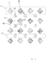
- the pixel arrangement structure comprises a plurality of first pixel rows 10 and a plurality of second pixel rows 20 arranged alternately.
- Each first pixel row 10 comprises a plurality of first sub-pixels 31 and a plurality of second sub-pixels 32 arranged alternately and at intervals
- each second pixel row comprises a plurality of third sub-pixels 33 arranged at intervals.
- Two first sub-pixels 31 and two second sub-pixels 32 adjacent to the third sub-pixel 33 form a virtual box SQ
- the third sub-pixel 33 is arranged in the virtual box SQ formed by the two first sub-pixels 31 and the two second sub-pixels 32 adjacent thereto, an area of the first sub-pixel 31 is same as an area of the second sub-pixel 32, and the area of the first sub-pixel 31 and the area of the second sub-pixel 32 are greater than an area of the third sub-pixel 33.
- a center of the first sub-pixel 31 coincides with a first vertex P1 of the virtual box SQ
- a center of the second sub-pixel 32 coincides with a second vertex P2 adjacent to the first vertex P1 of the virtual box SQ
- a center of the third sub-pixel 33 coincides with a center C of the virtual box SQ.
- shapes of the first sub-pixel 31, the second sub-pixel 32, and the third sub-pixel 33 are all square, and diagonal lines of each first sub-pixel 31 and each second sub-pixel 32 in each first pixel row 10 are on a same straight line, and a diagonal line of the third sub-pixel 33 is parallel to a diagonal line of the first sub-pixel 31. Therefore, four first sides of each first sub-pixel 31 are respectively opposite to four third sub-pixels 33 adjacent thereto, four first sides of each second sub-pixel 32 are respectively opposite to four third sub-pixels 33 adjacent thereto, and four first sides of each third sub-pixel 33 are respectively opposite to two first sub-pixels 31 and two second sub-pixels 32 adjacent thereto.
- the first sub-pixel 31, the second sub-pixel 32, and the third sub-pixel 33 have different colors and are one of a red sub-pixel, a blue sub-pixel, and a green sub-pixel.
- the first sub-pixel 31, the second sub-pixel 32, and the third sub-pixel 33 emit red light, blue light, and green light respectively.
- the first sub-pixel 31, the second sub-pixel 32, and the third sub-pixel 33 comprise organic light emitting diodes that emit red light, blue light, and green light, respectively. It is understood that, in other embodiments of the present invention, the first sub-pixel 31, the second sub-pixel 32, and the third sub-pixel 33 may also emit light of other colors.
- square sub-pixels in this embodiment have advantages over octagonal sub-pixels.
- a distance between the first sub-pixel 31a and the third sub-pixel and a distance between the second sub-pixel 32a and the third sub-pixel are both a first length Gap.
- an embodiment of the present invention increases an area of the first sub-pixel 31 and an area of the second sub-pixel 32 by setting both the first sub-pixel 31 and the second sub-pixel 32 to be square.
- an area of an organic light emitting diode is proportional to its lifetime, so that compared with the embodiment using the octagonal first sub-pixel 31a and the octagonal second sub-pixel 32a, the pixel arrangement of the first embodiment of the present invention has a longer lifetime without changing the first length.
- the shape of the third sub-pixel 33b is octagonal
- the area of the third sub-pixel is increased and lifetime of the OLED display panel is increased without changing the first length GAP.
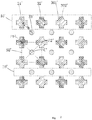
- the pixel arrangement structure comprises a plurality of first pixel rows 10' and a plurality of second pixel rows 20' arranged alternately.
- Each first pixel row 10' comprises a plurality of first sub-pixels 31' and a plurality of second sub-pixels 32' arranged alternately and at intervals, and each second pixel row comprises a plurality of third sub-pixels 33' arranged at intervals.
- Two first sub-pixels 31' and two second sub-pixels 32' adjacent to the third sub-pixel 33' form a virtual box SQ'
- the third sub-pixel 33' is arranged in the virtual box SQ' formed by the two first sub-pixels 31' and the two second sub-pixels 32' adjacent thereto, an area of the first sub-pixel 31' is same as an area of the second sub-pixel 32', and the area of the first sub-pixel 31' and the area of the second sub-pixel 32' are greater than an area of the third sub-pixel 33'.
- a center of the first sub-pixel 31' coincides with a first vertex P1' of the virtual box SQ'
- a center of the second sub-pixel 32' coincides with a second vertex P2' adjacent to the first vertex P1' of the virtual box SQ'
- a center of the third sub-pixel 33' coincides with a center C' of the virtual box SQ'.
- a shape of the third sub-pixel 33' is a circle.
- the first sub-pixel 31' and the second sub-pixel 32' both comprise four first sides 301' and four second sides 302', and the first sides 301' and the second sides 302' are alternately connected to form a closed figure.
- the first side 301' is an arc recessed toward an inside of the closed figure, and the second side 302' is a straight line. Therefore, four first sides 301' of each first sub-pixel 31' are respectively opposite to four third sub-pixels 33' adjacent to the first sub-pixel 31', four first sides 301' of each second sub-pixel 32' are respectively opposite to four third sub-pixels 33' adjacent to the second sub-pixel 32'.
- shapes of the first sub-pixel 31' and the second sub-pixel 32' should be exactly the same, and radii of curvature of four first sides 301' of each first sub-pixel 31' and each second sub-pixel 32' are also the same.
- shapes of the first sub-pixel 31' and the second sub-pixel 32' may be slightly different, and radii of curvature of four first sides 301' of each first sub-pixel 31' and each second sub-pixel 32' may also be slightly deviated, which will not affect the implementation of the present invention.
- the third sub-pixel 33' is set to a circle, and arc-shaped first sides 301' are set in the first sub-pixel 31' and the second sub-pixel 32', which is more in line with the principle of diffusion and can effectively reduce difficulty of making the FFM.
- the circular third sub-pixel 33' is the shape with the smallest side length and the highest efficiency in the same area. Due to halo effect of human eyes, a tiny non-circular luminous body will also be regarded as an approximately circular shape.
- Setting the third sub-pixel 33' as a circular shape can maximize efficiency of the third sub-pixel 33' and meet the halo effect of human eyes.
- the first sub-pixel 31', the second sub-pixel 32', and the third sub-pixel 33' have different colors and are one of a red sub-pixel, a blue sub-pixel, and a green sub-pixel.
- the first sub-pixel 31', the second sub-pixel 32', and the third sub-pixel 33' emit red light, blue light, and green light respectively.
- the first sub-pixel 31', the second sub-pixel 32', and the third sub-pixel 33' comprise organic light emitting diodes that emit red light, blue light, and green light, respectively. It is understood that, in other embodiments of the present invention, the first sub-pixel 31', the second sub-pixel 32', and the third sub-pixel 33' may also emit light of other colors.
- the second embodiment when a distance between the first sub-pixel and the third sub-pixel and a distance between the second sub-pixel and the third sub-pixel, i.e., the first length Gap, are constant, areas of the first sub-pixel 31' and the second sub-pixel 32' are larger, but the area of the third sub-pixel 33' is smaller.
- lifetime of an organic light emitting diode emitting blue light is the worst, while lifetime of an organic light emitting diode emitting green light is better.
- the overall lifetime of the OLED display panel depends on the organic light emitting diode with the worst lifetime.
- the third sub-pixel 33' corresponds to an organic light emitting diode that emits green light
- the second sub-pixel 32' corresponds to an organic light emitting diode that emits blue light.
- actual lifetime of the third sub-pixel 33' after the area thereof becomes smaller is still greater than actual lifetime of the second sub-pixel 32' after the area thereof becomes larger. Therefore, the overall lifetime of the OLED display panel still depends on the actual lifetime of the second sub-pixel 32'.
- the area of the second sub-pixel 32' is larger than that of the first embodiment, so that the overall lifetime of the OLED display panel is larger than that of the first embodiment.
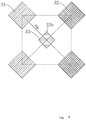
- a distance from the first side of the first sub-pixel 31' to an edge of the third sub-pixel 33' opposite to the first side 301' thereof and a distance from the first side 301' of the second sub-pixel 32' to an edge of the third sub-pixel 33' opposite to the first side 301' thereof are both a first length Gap
- a distance from a center of the first sub-pixel 31' to the first side 301' thereof and a distance from a center of the second sub-pixel 32' to the first side 301' thereof are both a second length b
- a radius of the third sub-pixel 33' is a third length r.
- a pixel density of the pixel arrangement structure preferably ranges from 200 ppi to 600 ppi
- the first length Gap preferably ranges from 10 um to 30 um
- the second length b preferably ranges from 10 um to 50 um
- the third length r preferably ranges from 4 um to 40 um.
- the first length Gap may be 20 um
- the pixel density of the pixel arrangement may be 200 ppi
- a sum of the second length b and the third length r may be 40 um
- the second length b may range from 10 um to 30 um.
- the first length Gap may be 20 um
- the pixel density of the pixel arrangement structure may be 250 ppi
- a sum of the second length b and the third length r may be 28 um
- the second length b may range from 10 um to 21 um.
- the first length Gap may be 20 um
- the pixel density of the pixel arrangement structure may be 300 ppi
- a sum of the second length b and the third length r may be 20 um
- the second length b may range from 10 um to 15 um.
- the first length Gap may be 20 um
- the pixel density of the pixel arrangement structure may be 350 ppi
- a sum of the second length b and the third length r may be 14 um
- the second length b may be 10 um.
- the first length Gap may be 15 um
- the pixel density of the pixel arrangement structure may be 200 ppi
- a sum of the second length b and the third length r may be 45 um
- the second length b may range from 10 um to 33 um.
- the first length Gap may be 15 um
- the pixel density of the pixel arrangement structure may be 250 ppi
- a sum of the second length b and the third length r may be 33 um
- the second length b may range from 10 um to 24 um.
- the first length Gap may be 15 um
- the pixel density of the pixel arrangement structure may be 300 ppi
- a sum of the second length and the third length may be 25um
- the second length b may range from 10 um to 18 um.
- the first length Gap may be 15 um
- the pixel density of the pixel arrangement structure may be 350 ppi
- a sum of the second length b and the third length r may be 19 um
- the second length b may range from 10 um to 14 um.
- the first length Gap may be 15 um
- the pixel density of the pixel arrangement structure may be 400 ppi
- a sum of the second length b and the third length r may be 15 um
- the second length b may range from 10 um to 11 um.
- the first length Gap may be 25 um
- the pixel density of the pixel arrangement structure may be 200 ppi
- a sum of the second length b and the third length r may be 35 um
- the second length b may range from 10 um to 26 um.
- the first length Gap may be 25 um
- the pixel density of the pixel arrangement structure may be 250 ppi
- a sum of the second length b and the third length r may be 23 um
- the second length b may range from 10 um to 17 um.
- the first length Gap may be 25 um
- the pixel density of the pixel arrangement structure may be 300 ppi
- a sum of the second length b and the third length r may be 15 um
- the second length b may range from 10 um to 11 um.
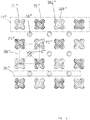
- the pixel arrangement structure comprises a plurality of first pixel rows 10" and a plurality of second pixel rows 20" arranged alternately.
- Each first pixel row 10" comprises a plurality of first sub-pixels 31" and a plurality of second sub-pixels 32" arranged alternately and at intervals
- each second pixel row comprises a plurality of third sub-pixels 33" arranged at intervals.
- Two first sub-pixels 31" and two second sub-pixels 32" adjacent to the third sub-pixel 33" form a virtual box SQ
- the third sub-pixel 33" is arranged in the virtual box SQ" formed by the two first sub-pixels 31" and the two second sub-pixels 32" adjacent thereto, an area of the first sub-pixel 31" is same as an area of the second sub-pixel 32", and the area of the first sub-pixel 31" and the area of the second sub-pixel 32" are greater than an area of the third sub-pixel 33".
- a center of the first sub-pixel 31" coincides with a first vertex P1" of the virtual box SQ
- a center of the second sub-pixel 32" coincides with a second vertex P2" adjacent to the first vertex P1" of the virtual box SQ
- a center of the third sub-pixel 33" coincides with a center C" of the virtual box SQ.
- a shape of the third sub-pixel 33" is a circle.
- the first sub-pixel 31" and the second sub-pixel 32" have the same shape and both comprise four first sides 301" and four second sides 302", and the first sides 301" and the second sides 302" are alternately connected to form a closed figure.
- the first side 301" is an arc recessed toward an inside of the closed figure
- the second side 302" is an arc protruding toward the inside of the closed figure, that is, the shape of the second side 302" is similar to a bow arm of an arrow.
- each first sub-pixel 31" can be set to be respectively opposite to four third sub-pixels 33" adjacent to the first sub-pixel 31
- four first sides 301" of each second sub-pixel 32" can be set to be respectively opposite to four third sub-pixels 33" adjacent to the second sub-pixel 32.
- four second sides 302" of each first sub-pixel 31" are set to be respectively opposite to four third sub-pixels 33" adjacent to the first sub-pixel 31
- four second sides 302" of each second sub-pixel 32" are set to be respectively opposite to four third sub-pixels 33" adjacent to the second sub-pixel 32".
- shapes of the first sub-pixel 31" and the second sub-pixel 32" should be exactly the same, radii of curvature of four first sides 301" of each first sub-pixel 31" and each second sub-pixel 32" are also the same, and radii of curvature of four second sides 302" of each first sub-pixel 31" and each second sub-pixel 32" are also the same.
- shapes of the first sub-pixel 31" and the second sub-pixel 32" may be slightly different, radii of curvature of four first sides 301" of each first sub-pixel 31" and each second sub-pixel 32" may also be slightly deviated, and radii of curvature of four second sides 302" of each first sub-pixel 31" and each second sub-pixel 32" may also be slightly deviated, which will not affect the implementation of the present invention.
- the third sub-pixel 33" is set to a circle, and arc-shaped first sides 301" and arc-shaped second sides 302" are set in the first sub-pixel 31" and the second sub-pixel 32", which is more in line with the principle of diffusion and can effectively reduce difficulty of making the FFM.
- the circular third sub-pixel 33" is the shape with the smallest side length and the highest efficiency in the same area. Due to halo effect of human eyes, a tiny non-circular luminous body will also be regarded as an approximately circular shape. Setting the third sub-pixel 33" as a circular shape can maximize efficiency of the third sub-pixel 33" and meet the halo effect of human eyes.
- the first sub-pixel 31", the second sub-pixel 32", and the third sub-pixel 33" have different colors and are one of a red sub-pixel, a blue sub-pixel, and a green sub-pixel.
- the first sub-pixel 31", the second sub-pixel 32", and the third sub-pixel 33" emit red light, blue light, and green light respectively.
- the first sub-pixel 31", the second sub-pixel 32", and the third sub-pixel 33" comprise organic light emitting diodes that emit red light, blue light, and green light, respectively. It is understood that, in other embodiments of the present invention, the first sub-pixel 31", the second sub-pixel 32", and the third sub-pixel 33" may also emit light of other colors.
- the second side 302" is an arc protruding toward an outside of the closed figure, so that areas of the first sub-pixel 31" and the second sub-pixel 32" are larger and lifetime can be further improved compared with the second embodiment.
- shapes and areas of the first sub-pixel and the second sub-pixel are completely the same, such that in the manufacturing process of the OLED display panel adopting the pixel arrangement structure of the present invention, the first sub-pixel and the second sub-pixel can be manufactured by using the same metal mask. This reduces production costs and enhances product competitiveness.
- an embodiment of the present invention provides a pixel arrangement structure comprising a plurality of first pixel rows and a plurality of second pixel rows arranged alternately.
- Each first pixel row comprises a plurality of first sub-pixels and a plurality of second sub-pixels arranged alternately and at intervals, and each second pixel row comprises a plurality of third sub-pixels arranged at intervals.
- Two first sub-pixels and two second sub-pixels adjacent to the third sub-pixel form a virtual box
- the third sub-pixel is arranged in the virtual box formed by the two first sub-pixels and the two second sub-pixels adjacent to the third sub-pixel, an area of the first sub-pixel is same as an area of the second sub-pixel, and the area of the first sub-pixel and the area of the second sub-pixel are greater than an area of the third sub-pixel.
- the pixel arrangement structure is applicable in an OLED display panel, which can reduce difficulty of manufacturing the OLED display panel and extend lifetime of the OLED display panel.
Landscapes
- Engineering & Computer Science (AREA)
- Physics & Mathematics (AREA)
- Computer Hardware Design (AREA)
- General Physics & Mathematics (AREA)
- Theoretical Computer Science (AREA)
- Electroluminescent Light Sources (AREA)
- Devices For Indicating Variable Information By Combining Individual Elements (AREA)
Applications Claiming Priority (2)
| Application Number | Priority Date | Filing Date | Title |
|---|---|---|---|
| CN201810103217.3A CN108364983A (zh) | 2018-02-01 | 2018-02-01 | 像素排列结构 |
| PCT/CN2018/077253 WO2019148558A1 (zh) | 2018-02-01 | 2018-02-26 | 像素排列结构 |
Publications (2)
| Publication Number | Publication Date |
|---|---|
| EP3748680A1 true EP3748680A1 (de) | 2020-12-09 |
| EP3748680A4 EP3748680A4 (de) | 2021-10-20 |
Family
ID=63004312
Family Applications (1)
| Application Number | Title | Priority Date | Filing Date |
|---|---|---|---|
| EP18904186.6A Pending EP3748680A4 (de) | 2018-02-01 | 2018-02-26 | Pixelanordnungsstruktur |
Country Status (6)
| Country | Link |
|---|---|
| US (1) | US10971054B2 (de) |
| EP (1) | EP3748680A4 (de) |
| JP (1) | JP6987261B2 (de) |
| KR (1) | KR102420761B1 (de) |
| CN (4) | CN108364983A (de) |
| WO (1) | WO2019148558A1 (de) |
Families Citing this family (38)
| Publication number | Priority date | Publication date | Assignee | Title |
|---|---|---|---|---|
| US11233096B2 (en) | 2016-02-18 | 2022-01-25 | Boe Technology Group Co., Ltd. | Pixel arrangement structure and driving method thereof, display substrate and display device |
| CN110137213B (zh) | 2018-02-09 | 2025-03-25 | 京东方科技集团股份有限公司 | 像素排列结构及其显示方法、显示基板 |
| WO2021016946A1 (zh) | 2019-07-31 | 2021-02-04 | 京东方科技集团股份有限公司 | 显示基板及其制备方法、显示面板、显示装置 |
| CN109994504A (zh) | 2018-01-02 | 2019-07-09 | 京东方科技集团股份有限公司 | 一种像素排布结构及相关装置 |
| US11889719B2 (en) | 2018-02-01 | 2024-01-30 | Wuhan China Star Optoelectronics Semiconductor Display Technology Co., Ltd. | Display panel |
| CN109686777B (zh) * | 2019-01-31 | 2020-12-04 | 武汉华星光电半导体显示技术有限公司 | 显示面板 |
| CN108364983A (zh) * | 2018-02-01 | 2018-08-03 | 武汉华星光电半导体显示技术有限公司 | 像素排列结构 |
| US11355556B2 (en) * | 2018-02-01 | 2022-06-07 | Wuhan China Star Optoelectronics Semiconductor Display Technology Co., Ltd. | Display panel |
| US11522019B2 (en) | 2018-02-01 | 2022-12-06 | Wuhan China Star Optoelectronics Semiconductor Display Technology Co., Ltd. | Display panel |
| CN109637388B (zh) * | 2019-01-31 | 2020-06-16 | 武汉华星光电半导体显示技术有限公司 | 显示面板 |
| CN109817682B (zh) | 2019-01-31 | 2020-12-25 | 武汉华星光电半导体显示技术有限公司 | 显示面板 |
| CN110137211A (zh) * | 2018-02-09 | 2019-08-16 | 京东方科技集团股份有限公司 | 一种像素排布结构、高精度金属掩模板及显示装置 |
| CN109935617B (zh) * | 2018-11-30 | 2024-04-05 | 京东方科技集团股份有限公司 | 像素排列结构、显示基板以及掩模板组 |
| CN113823240B (zh) * | 2018-12-13 | 2023-04-18 | 京东方科技集团股份有限公司 | 显示装置 |
| CN109817683B (zh) * | 2019-01-31 | 2021-05-28 | 武汉华星光电半导体显示技术有限公司 | 显示面板 |
| CN111834428B (zh) * | 2019-01-31 | 2023-07-04 | 武汉华星光电半导体显示技术有限公司 | 显示面板 |
| CN109768073B (zh) * | 2019-02-26 | 2021-04-27 | 武汉华星光电半导体显示技术有限公司 | 有机发光二极管显示器像素排列结构及显示面板 |
| CN110518047B (zh) * | 2019-08-30 | 2022-01-14 | 武汉天马微电子有限公司 | 像素结构、显示面板及显示装置 |
| CN110620135B (zh) * | 2019-09-30 | 2022-05-27 | 武汉天马微电子有限公司 | 一种显示面板及显示装置 |
| CN110867481B (zh) * | 2019-12-17 | 2022-12-06 | 武汉天马微电子有限公司 | 像素排列结构、显示面板及显示装置 |
| CN111489645B (zh) | 2020-04-23 | 2022-06-24 | 京东方科技集团股份有限公司 | 一种显示基板及其制造方法、显示装置 |
| CN112420785B (zh) * | 2020-11-05 | 2023-05-09 | 深圳市华星光电半导体显示技术有限公司 | Oled显示面板 |
| WO2022141628A1 (zh) * | 2021-01-04 | 2022-07-07 | 京东方科技集团股份有限公司 | 一种显示基板及相关装置 |
| CN112992997B (zh) * | 2021-02-09 | 2024-04-19 | 京东方科技集团股份有限公司 | 一种像素结构、显示基板、显示装置及显示方法 |
| CN113053973B (zh) * | 2021-03-11 | 2023-04-07 | 云南创视界光电科技有限公司 | 显示基板、彩膜基板、显示面板及显示装置 |
| CN113178461A (zh) * | 2021-04-07 | 2021-07-27 | 武汉华星光电半导体显示技术有限公司 | 像素结构及掩膜板 |
| CN113130609B (zh) * | 2021-04-09 | 2025-01-17 | 京东方科技集团股份有限公司 | 显示面板、显示装置和掩模板 |
| CN115605056A (zh) * | 2021-07-09 | 2023-01-13 | 南方科技大学(Cn) | 一种像素排列结构及显示面板 |
| CN113594221B (zh) * | 2021-07-30 | 2022-07-22 | 科迪华显示技术(绍兴)有限公司 | 透明显示面板及其制造方法、透明显示装置 |
| EP4350735A4 (de) * | 2021-10-14 | 2024-11-27 | BOE Technology Group Co., Ltd. | Anzeigetafel und anzeigevorrichtung |
| CN113888978B (zh) * | 2021-10-20 | 2022-09-09 | 武汉华星光电半导体显示技术有限公司 | 柔性显示模组及移动终端 |
| CN114156332B (zh) * | 2021-12-13 | 2025-12-23 | 昆山国显光电有限公司 | 像素排布结构、显示面板和显示装置 |
| CN114420741B (zh) * | 2022-02-28 | 2026-01-27 | 京东方科技集团股份有限公司 | 一种像素结构和显示面板 |
| CN117255584A (zh) | 2022-06-06 | 2023-12-19 | 上海和辉光电股份有限公司 | 像素阵列、显示面板和金属掩膜板 |
| CN117939954A (zh) * | 2022-10-10 | 2024-04-26 | 华为技术有限公司 | 像素排列结构、电子设备、显示面板和制备方法 |
| US20260052843A1 (en) * | 2022-11-22 | 2026-02-19 | Chengdu Boe Optoelectronics Technology Co., Ltd. | Display substrate and display device |
| CN117479710A (zh) * | 2023-02-07 | 2024-01-30 | 武汉华星光电半导体显示技术有限公司 | 像素结构、显示面板 |
| CN119923988A (zh) * | 2023-08-30 | 2025-05-02 | 京东方科技集团股份有限公司 | 像素排布结构、显示面板和显示装置 |
Family Cites Families (33)
| Publication number | Priority date | Publication date | Assignee | Title |
|---|---|---|---|---|
| US7274383B1 (en) * | 2000-07-28 | 2007-09-25 | Clairvoyante, Inc | Arrangement of color pixels for full color imaging devices with simplified addressing |
| JP2007017477A (ja) * | 2005-07-05 | 2007-01-25 | Seiko Epson Corp | 画素配列構造 |
| GB2437110B (en) * | 2006-04-12 | 2009-01-28 | Cambridge Display Tech Ltd | Optoelectronic display and method of manufacturing the same |
| KR101023133B1 (ko) * | 2009-03-19 | 2011-03-18 | 삼성모바일디스플레이주식회사 | 유기 발광 표시 장치 |
| KR20110021090A (ko) * | 2009-08-25 | 2011-03-04 | 엘지디스플레이 주식회사 | 유기전계 발광소자 제조 용 쉐도우 마스크 |
| KR101615332B1 (ko) * | 2012-03-06 | 2016-04-26 | 삼성디스플레이 주식회사 | 유기 발광 표시 장치의 화소 배열 구조 |
| JP6494525B2 (ja) * | 2013-01-17 | 2019-04-03 | カティーバ, インコーポレイテッド | 高解像度有機発光ダイオードデバイス、ディスプレイ、および関連方法 |
| KR102072216B1 (ko) * | 2013-03-26 | 2020-02-03 | 삼성디스플레이 주식회사 | 유기 발광 표시 장치 |
| CN103219359A (zh) * | 2013-03-29 | 2013-07-24 | 京东方科技集团股份有限公司 | 有机电致发光阵列基板及其制作方法、显示装置 |
| KR101485166B1 (ko) * | 2013-04-25 | 2015-01-22 | 삼성디스플레이 주식회사 | 유기 발광 표시 장치 및 마스크 유닛 |
| TWI674671B (zh) * | 2013-05-28 | 2019-10-11 | 日商新力股份有限公司 | 顯示裝置及電子機器 |
| CN103366683B (zh) * | 2013-07-12 | 2014-10-29 | 上海和辉光电有限公司 | 像素阵列、显示器以及将图像呈现于显示器上的方法 |
| KR102103499B1 (ko) * | 2013-10-16 | 2020-04-23 | 삼성디스플레이 주식회사 | 유기 발광 표시 장치 |
| CN103745684B (zh) * | 2013-11-13 | 2016-09-28 | 上海和辉光电有限公司 | 像素阵列、呈现图像于显示器上的方法及显示器 |
| CN103985738B (zh) * | 2014-05-08 | 2015-06-17 | 京东方科技集团股份有限公司 | 像素结构和显示装置 |
| JP6459243B2 (ja) * | 2014-06-26 | 2019-01-30 | Tianma Japan株式会社 | 画素アレイ及びメタルマスク並びに電気光学装置並びに電気機器 |
| CN104282727B (zh) * | 2014-09-30 | 2017-08-29 | 京东方科技集团股份有限公司 | 一种像素结构及其显示方法、显示装置 |
| CN104576695B (zh) * | 2014-12-22 | 2017-08-25 | 信利(惠州)智能显示有限公司 | Oled像素排列结构及显示装置 |
| CN104576699B (zh) * | 2014-12-26 | 2017-08-25 | 信利(惠州)智能显示有限公司 | 一种有机发光二极管显示器的像素排列结构 |
| US9780150B2 (en) * | 2015-02-16 | 2017-10-03 | Shanghai Tianma AM-OLED Co., Ltd. | Organic light emitting diode display device and manufacturing method thereof |
| KR102491117B1 (ko) * | 2015-07-07 | 2023-01-20 | 삼성디스플레이 주식회사 | 유기 발광 표시 장치 |
| CN105047092B (zh) * | 2015-08-06 | 2018-07-06 | 上海和辉光电有限公司 | 显示器及其像素阵列 |
| CN204885166U (zh) * | 2015-09-09 | 2015-12-16 | 昆山国显光电有限公司 | 像素结构和oled显示面板 |
| CN106816449A (zh) * | 2015-12-01 | 2017-06-09 | 昆山国显光电有限公司 | Oled显示屏及其像素结构、oled显示屏的制作方法 |
| CN107221547B (zh) * | 2016-03-22 | 2020-04-14 | 群创光电股份有限公司 | 显示设备 |
| KR102691719B1 (ko) * | 2016-04-20 | 2024-08-05 | 엘지디스플레이 주식회사 | 유기 발광 표시 장치 |
| CN106298851B (zh) * | 2016-08-12 | 2018-06-29 | 京东方科技集团股份有限公司 | 一种像素结构、显示面板及其驱动方法 |
| CN106298855B (zh) * | 2016-08-29 | 2019-03-15 | 昆山国显光电有限公司 | 像素结构及oled显示装置 |
| CN106648200B (zh) * | 2016-09-23 | 2019-03-29 | 上海天马微电子有限公司 | 一种oled阵列基板、显示面板及显示装置 |
| CN206340547U (zh) * | 2016-12-26 | 2017-07-18 | 云谷(固安)科技有限公司 | Oled像素排布结构、金属掩膜板及oled显示屏 |
| CN109427850B (zh) * | 2017-08-31 | 2020-02-21 | 昆山国显光电有限公司 | 像素结构及包含所述像素结构的显示面板 |
| CN109994509B (zh) * | 2018-01-02 | 2025-01-03 | 京东方科技集团股份有限公司 | 一种像素排布结构及相关装置 |
| CN108364983A (zh) * | 2018-02-01 | 2018-08-03 | 武汉华星光电半导体显示技术有限公司 | 像素排列结构 |
-
2018
- 2018-02-01 CN CN201810103217.3A patent/CN108364983A/zh not_active Withdrawn
- 2018-02-26 CN CN202010631408.4A patent/CN111863887B/zh active Active
- 2018-02-26 CN CN201880067061.6A patent/CN111226320A/zh active Pending
- 2018-02-26 KR KR1020207022159A patent/KR102420761B1/ko active Active
- 2018-02-26 CN CN202110324984.9A patent/CN113053986B/zh active Active
- 2018-02-26 EP EP18904186.6A patent/EP3748680A4/de active Pending
- 2018-02-26 JP JP2020541411A patent/JP6987261B2/ja active Active
- 2018-02-26 WO PCT/CN2018/077253 patent/WO2019148558A1/zh not_active Ceased
-
2020
- 2020-07-29 US US16/941,817 patent/US10971054B2/en active Active
Also Published As
| Publication number | Publication date |
|---|---|
| KR20200101455A (ko) | 2020-08-27 |
| JP6987261B2 (ja) | 2021-12-22 |
| CN111863887A (zh) | 2020-10-30 |
| KR102420761B1 (ko) | 2022-07-14 |
| US10971054B2 (en) | 2021-04-06 |
| JP2021511551A (ja) | 2021-05-06 |
| CN111226320A (zh) | 2020-06-02 |
| CN111863887A8 (zh) | 2021-01-26 |
| WO2019148558A1 (zh) | 2019-08-08 |
| CN108364983A (zh) | 2018-08-03 |
| CN111863887B (zh) | 2021-04-02 |
| US20200357325A1 (en) | 2020-11-12 |
| CN113053986B (zh) | 2022-09-27 |
| CN113053986A (zh) | 2021-06-29 |
| EP3748680A4 (de) | 2021-10-20 |
Similar Documents
| Publication | Publication Date | Title |
|---|---|---|
| EP3748680A1 (de) | Pixelanordnungsstruktur | |
| US11561465B2 (en) | Pixel arrangement structure, organic light emitting device, display device and mask | |
| CN108807491B (zh) | 像素排列结构 | |
| US10692940B2 (en) | Pixel structure and display panel having the same | |
| US20180175121A1 (en) | Pixel arrangement structure, organic light-emitting diode device, display device and mask | |
| US10170526B1 (en) | Organic light emitting diode display panel and method for manufacturing same | |
| KR102904709B1 (ko) | 픽셀 배열 구조, 디스플레이 패널 및 디스플레이 장치 | |
| US20150236077A1 (en) | Oled display | |
| US11024676B2 (en) | Organic light-emitting diode display panel and manufacturing method thereof, and display device | |
| KR20150005845A (ko) | 유기 발광 표시 장치 | |
| US11889719B2 (en) | Display panel | |
| KR20120041510A (ko) | 유기전계 발광소자 및 이를 제조하기 위한 쉐도우 마스크 | |
| CN110707141A (zh) | 有机发光显示基板及显示装置 | |
| US11522019B2 (en) | Display panel | |
| CN117529146A (zh) | 显示面板和显示装置 | |
| KR20110108049A (ko) | 유기전계발광소자 및 이의 제조방법 | |
| CN110634909A (zh) | 一种显示基板、显示面板及显示装置 | |
| JP2018507526A (ja) | ディスプレイパネル | |
| US20220115457A1 (en) | Pixel arrangement structure and oled display device | |
| CN115811916B (zh) | 显示面板和显示装置 | |
| US20210335899A1 (en) | Organic light-emitting diode display | |
| KR100732429B1 (ko) | 유기 발광 소자 | |
| CN111081889B (zh) | 照明装置 | |
| CN118510340A (zh) | 一种oled像素排布结构、显示面板和显示装置 | |
| KR20050083448A (ko) | 새도우 마스크 |
Legal Events
| Date | Code | Title | Description |
|---|---|---|---|
| STAA | Information on the status of an ep patent application or granted ep patent |
Free format text: STATUS: THE INTERNATIONAL PUBLICATION HAS BEEN MADE |
|
| PUAI | Public reference made under article 153(3) epc to a published international application that has entered the european phase |
Free format text: ORIGINAL CODE: 0009012 |
|
| STAA | Information on the status of an ep patent application or granted ep patent |
Free format text: STATUS: REQUEST FOR EXAMINATION WAS MADE |
|
| 17P | Request for examination filed |
Effective date: 20200724 |
|
| AK | Designated contracting states |
Kind code of ref document: A1 Designated state(s): AL AT BE BG CH CY CZ DE DK EE ES FI FR GB GR HR HU IE IS IT LI LT LU LV MC MK MT NL NO PL PT RO RS SE SI SK SM TR |
|
| AX | Request for extension of the european patent |
Extension state: BA ME |
|
| DAV | Request for validation of the european patent (deleted) | ||
| DAX | Request for extension of the european patent (deleted) | ||
| A4 | Supplementary search report drawn up and despatched |
Effective date: 20210916 |
|
| RIC1 | Information provided on ipc code assigned before grant |
Ipc: H01L 27/32 20060101AFI20210910BHEP |
|
| STAA | Information on the status of an ep patent application or granted ep patent |
Free format text: STATUS: EXAMINATION IS IN PROGRESS |
|
| 17Q | First examination report despatched |
Effective date: 20240828 |