EP3738136B1 - Komponenten und verfahren zur verwaltung von plasmaprozessnebenproduktmaterialien - Google Patents
Komponenten und verfahren zur verwaltung von plasmaprozessnebenproduktmaterialien Download PDFInfo
- Publication number
- EP3738136B1 EP3738136B1 EP19736155.3A EP19736155A EP3738136B1 EP 3738136 B1 EP3738136 B1 EP 3738136B1 EP 19736155 A EP19736155 A EP 19736155A EP 3738136 B1 EP3738136 B1 EP 3738136B1
- Authority
- EP
- European Patent Office
- Prior art keywords
- ring structure
- chamber
- substrate
- plasma
- plasma process
- Prior art date
- Legal status (The legal status is an assumption and is not a legal conclusion. Google has not performed a legal analysis and makes no representation as to the accuracy of the status listed.)
- Active
Links
Images


Classifications
-
- B—PERFORMING OPERATIONS; TRANSPORTING
- B24—GRINDING; POLISHING
- B24C—ABRASIVE OR RELATED BLASTING WITH PARTICULATE MATERIAL
- B24C1/00—Methods for use of abrasive blasting for producing particular effects; Use of auxiliary equipment in connection with such methods
- B24C1/06—Methods for use of abrasive blasting for producing particular effects; Use of auxiliary equipment in connection with such methods for producing matt surfaces, e.g. on plastic materials, on glass
-
- C—CHEMISTRY; METALLURGY
- C23—COATING METALLIC MATERIAL; COATING MATERIAL WITH METALLIC MATERIAL; CHEMICAL SURFACE TREATMENT; DIFFUSION TREATMENT OF METALLIC MATERIAL; COATING BY VACUUM EVAPORATION, BY SPUTTERING, BY ION IMPLANTATION OR BY CHEMICAL VAPOUR DEPOSITION, IN GENERAL; INHIBITING CORROSION OF METALLIC MATERIAL OR INCRUSTATION IN GENERAL
- C23C—COATING METALLIC MATERIAL; COATING MATERIAL WITH METALLIC MATERIAL; SURFACE TREATMENT OF METALLIC MATERIAL BY DIFFUSION INTO THE SURFACE, BY CHEMICAL CONVERSION OR SUBSTITUTION; COATING BY VACUUM EVAPORATION, BY SPUTTERING, BY ION IMPLANTATION OR BY CHEMICAL VAPOUR DEPOSITION, IN GENERAL
- C23C16/00—Chemical coating by decomposition of gaseous compounds, without leaving reaction products of surface material in the coating, i.e. chemical vapour deposition [CVD] processes
- C23C16/44—Chemical coating by decomposition of gaseous compounds, without leaving reaction products of surface material in the coating, i.e. chemical vapour deposition [CVD] processes characterised by the method of coating
- C23C16/4401—Means for minimising impurities, e.g. dust, moisture or residual gas, in the reaction chamber
- C23C16/4404—Coatings or surface treatment on the inside of the reaction chamber or on parts thereof
-
- C—CHEMISTRY; METALLURGY
- C23—COATING METALLIC MATERIAL; COATING MATERIAL WITH METALLIC MATERIAL; CHEMICAL SURFACE TREATMENT; DIFFUSION TREATMENT OF METALLIC MATERIAL; COATING BY VACUUM EVAPORATION, BY SPUTTERING, BY ION IMPLANTATION OR BY CHEMICAL VAPOUR DEPOSITION, IN GENERAL; INHIBITING CORROSION OF METALLIC MATERIAL OR INCRUSTATION IN GENERAL
- C23C—COATING METALLIC MATERIAL; COATING MATERIAL WITH METALLIC MATERIAL; SURFACE TREATMENT OF METALLIC MATERIAL BY DIFFUSION INTO THE SURFACE, BY CHEMICAL CONVERSION OR SUBSTITUTION; COATING BY VACUUM EVAPORATION, BY SPUTTERING, BY ION IMPLANTATION OR BY CHEMICAL VAPOUR DEPOSITION, IN GENERAL
- C23C16/00—Chemical coating by decomposition of gaseous compounds, without leaving reaction products of surface material in the coating, i.e. chemical vapour deposition [CVD] processes
- C23C16/44—Chemical coating by decomposition of gaseous compounds, without leaving reaction products of surface material in the coating, i.e. chemical vapour deposition [CVD] processes characterised by the method of coating
- C23C16/4412—Details relating to the exhausts, e.g. pumps, filters, scrubbers, particle traps
-
- C—CHEMISTRY; METALLURGY
- C23—COATING METALLIC MATERIAL; COATING MATERIAL WITH METALLIC MATERIAL; CHEMICAL SURFACE TREATMENT; DIFFUSION TREATMENT OF METALLIC MATERIAL; COATING BY VACUUM EVAPORATION, BY SPUTTERING, BY ION IMPLANTATION OR BY CHEMICAL VAPOUR DEPOSITION, IN GENERAL; INHIBITING CORROSION OF METALLIC MATERIAL OR INCRUSTATION IN GENERAL
- C23C—COATING METALLIC MATERIAL; COATING MATERIAL WITH METALLIC MATERIAL; SURFACE TREATMENT OF METALLIC MATERIAL BY DIFFUSION INTO THE SURFACE, BY CHEMICAL CONVERSION OR SUBSTITUTION; COATING BY VACUUM EVAPORATION, BY SPUTTERING, BY ION IMPLANTATION OR BY CHEMICAL VAPOUR DEPOSITION, IN GENERAL
- C23C16/00—Chemical coating by decomposition of gaseous compounds, without leaving reaction products of surface material in the coating, i.e. chemical vapour deposition [CVD] processes
- C23C16/44—Chemical coating by decomposition of gaseous compounds, without leaving reaction products of surface material in the coating, i.e. chemical vapour deposition [CVD] processes characterised by the method of coating
- C23C16/458—Chemical coating by decomposition of gaseous compounds, without leaving reaction products of surface material in the coating, i.e. chemical vapour deposition [CVD] processes characterised by the method of coating characterised by the method used for supporting substrates in the reaction chamber
- C23C16/4582—Rigid and flat substrates, e.g. plates or discs
- C23C16/4583—Rigid and flat substrates, e.g. plates or discs the substrate being supported substantially horizontally
- C23C16/4585—Devices at or outside the perimeter of the substrate support, e.g. clamping rings, shrouds
-
- H—ELECTRICITY
- H01—ELECTRIC ELEMENTS
- H01J—ELECTRIC DISCHARGE TUBES OR DISCHARGE LAMPS
- H01J37/00—Discharge tubes with provision for introducing objects or material to be exposed to the discharge, e.g. for the purpose of examination or processing thereof
- H01J37/32—Gas-filled discharge tubes
- H01J37/32009—Arrangements for generation of plasma specially adapted for examination or treatment of objects, e.g. plasma sources
- H01J37/32082—Radio frequency generated discharge
- H01J37/321—Radio frequency generated discharge the radio frequency energy being inductively coupled to the plasma
- H01J37/32119—Windows
-
- H—ELECTRICITY
- H01—ELECTRIC ELEMENTS
- H01J—ELECTRIC DISCHARGE TUBES OR DISCHARGE LAMPS
- H01J37/00—Discharge tubes with provision for introducing objects or material to be exposed to the discharge, e.g. for the purpose of examination or processing thereof
- H01J37/32—Gas-filled discharge tubes
- H01J37/32431—Constructional details of the reactor
- H01J37/32458—Vessel
- H01J37/32467—Material
-
- H—ELECTRICITY
- H01—ELECTRIC ELEMENTS
- H01J—ELECTRIC DISCHARGE TUBES OR DISCHARGE LAMPS
- H01J37/00—Discharge tubes with provision for introducing objects or material to be exposed to the discharge, e.g. for the purpose of examination or processing thereof
- H01J37/32—Gas-filled discharge tubes
- H01J37/32431—Constructional details of the reactor
- H01J37/32458—Vessel
- H01J37/32477—Vessel characterised by the means for protecting vessels or internal parts, e.g. coatings
- H01J37/32495—Means for protecting the vessel against plasma
-
- H—ELECTRICITY
- H01—ELECTRIC ELEMENTS
- H01J—ELECTRIC DISCHARGE TUBES OR DISCHARGE LAMPS
- H01J37/00—Discharge tubes with provision for introducing objects or material to be exposed to the discharge, e.g. for the purpose of examination or processing thereof
- H01J37/32—Gas-filled discharge tubes
- H01J37/32431—Constructional details of the reactor
- H01J37/32458—Vessel
- H01J37/32477—Vessel characterised by the means for protecting vessels or internal parts, e.g. coatings
- H01J37/32504—Means for preventing sputtering of the vessel
-
- H—ELECTRICITY
- H01—ELECTRIC ELEMENTS
- H01J—ELECTRIC DISCHARGE TUBES OR DISCHARGE LAMPS
- H01J37/00—Discharge tubes with provision for introducing objects or material to be exposed to the discharge, e.g. for the purpose of examination or processing thereof
- H01J37/32—Gas-filled discharge tubes
- H01J37/32431—Constructional details of the reactor
- H01J37/32623—Mechanical discharge control means
- H01J37/32642—Focus rings
-
- H—ELECTRICITY
- H01—ELECTRIC ELEMENTS
- H01J—ELECTRIC DISCHARGE TUBES OR DISCHARGE LAMPS
- H01J37/00—Discharge tubes with provision for introducing objects or material to be exposed to the discharge, e.g. for the purpose of examination or processing thereof
- H01J37/32—Gas-filled discharge tubes
- H01J37/32431—Constructional details of the reactor
- H01J37/32623—Mechanical discharge control means
- H01J37/32651—Shields, e.g. dark space shields, Faraday shields
-
- H—ELECTRICITY
- H01—ELECTRIC ELEMENTS
- H01J—ELECTRIC DISCHARGE TUBES OR DISCHARGE LAMPS
- H01J37/00—Discharge tubes with provision for introducing objects or material to be exposed to the discharge, e.g. for the purpose of examination or processing thereof
- H01J37/32—Gas-filled discharge tubes
- H01J37/32431—Constructional details of the reactor
- H01J37/32733—Means for moving the material to be treated
- H01J37/32743—Means for moving the material to be treated for introducing the material into processing chamber
-
- H—ELECTRICITY
- H01—ELECTRIC ELEMENTS
- H01J—ELECTRIC DISCHARGE TUBES OR DISCHARGE LAMPS
- H01J37/00—Discharge tubes with provision for introducing objects or material to be exposed to the discharge, e.g. for the purpose of examination or processing thereof
- H01J37/32—Gas-filled discharge tubes
- H01J37/32431—Constructional details of the reactor
- H01J37/32798—Further details of plasma apparatus not provided for in groups H01J37/3244 - H01J37/32788; special provisions for cleaning or maintenance of the apparatus
- H01J37/32853—Hygiene
- H01J37/32871—Means for trapping or directing unwanted particles
-
- H—ELECTRICITY
- H01—ELECTRIC ELEMENTS
- H01J—ELECTRIC DISCHARGE TUBES OR DISCHARGE LAMPS
- H01J2237/00—Discharge tubes exposing object to beam, e.g. for analysis treatment, etching, imaging
- H01J2237/32—Processing objects by plasma generation
- H01J2237/33—Processing objects by plasma generation characterised by the type of processing
- H01J2237/334—Etching
-
- H—ELECTRICITY
- H01—ELECTRIC ELEMENTS
- H01J—ELECTRIC DISCHARGE TUBES OR DISCHARGE LAMPS
- H01J37/00—Discharge tubes with provision for introducing objects or material to be exposed to the discharge, e.g. for the purpose of examination or processing thereof
- H01J37/32—Gas-filled discharge tubes
- H01J37/32009—Arrangements for generation of plasma specially adapted for examination or treatment of objects, e.g. plasma sources
- H01J37/32082—Radio frequency generated discharge
- H01J37/32174—Circuits specially adapted for controlling the RF discharge
- H01J37/32183—Matching circuits
Definitions
- the present invention relates to semiconductor device fabrication.
- a process gas is transformed into a plasma within a processing chamber in which a substrate is positioned.
- the substrate is exposed to the plasma to produce a desired effect on the substrate, such as to etch/remove material from the substrate, and/or deposit material on the substrate, and/or modify a characteristic of a material on the substrate.
- non-volatile and/or low-volatility plasma process byproduct materials can be generated within the processing chamber.
- these byproduct materials deposit and buildup on various components with the processing chamber, various problems can occur.
- the byproduct materials can flake-off and/or peel-off of components and land on surfaces within the processing chamber that should remain contaminant-free, such as a substrate support structure and the substrate itself.
- US2009261065A1 discloses components for use in a plasma chamber, the components being made of ceramic with etched surfaces.
- WO03003404A2 discloses a domed enclosure wall for a plasma processing chamber that is made from a dielectric material having a roughened surface.
- a focus ring according to an aspect of the invention is set out in claim 1.
- Optional features of the focus ring are set out in claims 2-12.
- a method according to an aspect of the invention is set out in claim 13.
- Optional features of the method are set out in claim 14.
- a surface-textured plasma process chamber component is disclosed as a ceramic component configured for placement within a plasma process chamber, where the ceramic component includes at least one roughened surface oriented to be in exposure to plasma process byproduct material when the ceramic component is placed within the plasma process chamber during operation of the plasma process chamber.
- the at least one roughened surface is configured to promote adherence of the plasma process byproduct material to the ceramic component.
- a method for plasma processing of a substrate.
- the method includes having a plasma process chamber that includes a substrate support structure and a top window structure.
- the substrate support structure is configured to hold the substrate in exposure to a plasma.
- the top window structure is positioned above the substrate support structure to establish a plasma processing region between the substrate support structure and the top window structure.
- the top window structure is formed of ceramic material.
- the top window structure has a bottom surface facing the plasma processing region.
- the bottom surface has a surface roughness that promotes adherence of plasma process byproduct material to the bottom surface.
- the method also includes generating a plasma in the plasma processing region. Constituents of the plasma interact with a material on the substrate to generate plasma process byproduct material, with some of the plasma process byproduct material adhering to the bottom surface of the top window structure.
- a method for manufacturing a component for use within a plasma process chamber.
- the method includes forming a ceramic component for installation within a plasma process chamber.
- the ceramic component has at least one process-exposed surface.
- the method also includes roughening the at least one process-exposed surface to have a surface roughness average within a range extending from about 150 microinches to about 500 microinches (3.8 ⁇ m to about 12.7 ⁇ m).
- a method for converting a coated component for use within a plasma process chamber into a surface-roughened component for use within the plasma process chamber.
- the method includes stripping a coating from a ceramic component down to a bare ceramic material of which the ceramic component is formed.
- the ceramic component is configured for installation within a plasma process chamber.
- the ceramic component has at least one process-exposed surface.
- the method also includes roughening the at least one process-exposed surface to have a surface roughness average within a range extending from about 150 microinches to about 500 microinches (3.8 ⁇ m to about 12.7 ⁇ m).
- a focus ring for use in a plasma process chamber.
- the focus ring includes a ring structure formed of a ceramic material.
- the ring structure is configured to circumscribe a substrate support structure within a plasma process chamber.
- the ring structure has an inner surface oriented to be in exposure to plasma process byproduct material when the ring structure is placed within the plasma process chamber during operation of the plasma process chamber.
- the inner surface is formed to have a controlled surface topographical variation that promotes adherence of the plasma process byproduct material to the inner surface.
- a plasma process chamber in an example, includes a substrate support structure configured to hold a substrate in exposure to a plasma during operation of the plasma process chamber.
- the plasma process chamber also includes a focus ring including a ring structure formed of a ceramic material.
- the ring structure is configured to circumscribe the substrate support structure within the plasma process chamber.
- the ring structure has an inner surface oriented to be in exposure to plasma process byproduct material during operation of the plasma process chamber.
- the inner surface is formed to have a controlled surface topographical variation that promotes adherence of the plasma process byproduct material to the inner surface.
- a method for plasma processing of a substrate.
- the method includes having a plasma process chamber that includes a substrate support structure and a focus ring.
- the focus ring includes a ring structure formed of a ceramic material.
- the ring structure is configured to circumscribe the substrate support structure within the plasma process chamber.
- the ring structure has an inner surface oriented to be in exposure to plasma process byproduct material during operation of the plasma process chamber.
- the inner surface is formed to have a controlled surface topographical variation that promotes adherence of the plasma process byproduct material to the inner surface.
- the method also includes generating a plasma in a plasma processing region above the substrate support structure. Constituents of the plasma interact with a material on the substrate to generate plasma process byproduct material, with some of the plasma process byproduct material adhering to the inner surface of the ring structure.
- a plasma process chamber in an example, includes a substrate support structure configured to hold a substrate in exposure to a plasma during operation of the plasma process chamber.
- the plasma process chamber also includes a focus ring structure configured to circumscribe the substrate support structure within the plasma process chamber.
- the focus ring structure includes a ring portion formed as a right circular hollow cylinder and three radial extension structures configured to extend radially outward from an outer surface of the ring portion. The three radial extension structures are spaced apart along an outer perimeter of the ring portion.
- the plasma process chamber also includes an integral shield structure that includes a shield segment, a first support segment, and a second support segment. The first support segment extends from a first end of the shield segment.
- the first support segment is configured to engage with a first of the three radial extension structures of the focus ring structure.
- the second support segment extends from a second end of the shield segment.
- the second support segment is configured to engage with a second of the three radial extension structures of the focus ring structure.
- the integral shield structure is formed to extend along an arc.
- the shield segment is configured to at least partially cover a substrate access port opening of the plasma process chamber when the focus ring structure is in a lowered vertical position.
- the shield segment is configured to uncover the substrate access port opening of the plasma process chamber when the focus ring structure is in a raised vertical position.
- the method also includes positioning the focus ring structure in the lowered vertical position.
- the method also includes generating a plasma in a plasma processing region above the substrate support structure.
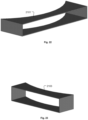
- a method for manufacturing a substrate access port shield for use in a plasma process chamber.
- the method includes forming an integral shield structure to include a shield segment, a first support segment extending from a first end of the shield segment, and a second support segment extending from a second end of the shield segment.
- the first support segment is configured to engage with a vertically movable component within the plasma process chamber.
- the second support segment is configured to engage with the vertically movable component within the plasma process chamber.
- the integral shield structure is formed to extend along an arc.
- the shield segment is configured to at least partially cover a substrate access port opening of the plasma process chamber when the first and second support segments are engaged with the vertically movable component and the vertically movable component is in a lowered vertical position.
- the shield segment is configured to uncover the substrate access port opening of the plasma process chamber when the first and second support segments are engaged with the vertically movable component and the vertically movable component is in a raised vertical position.
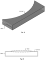
- an insert liner for a port of a plasma process chamber is disclosed.
- the insert liner is configured to cover an inner surface of the port formed through a wall of the plasma process chamber.
- the insert liner is configured to have mechanical flexibility sufficient for compression of an outer surface profile of the insert liner to enable insertion of the insert liner into the port.
- the insert liner is configured to impart a spring force against the inner surface of the port upon release of compression of the outer surface profile of the insert liner.
- a method for plasma processing of a substrate.
- the method includes having a plasma process chamber that includes a plasma processing region in which a plasma is generated during operation of the plasma process chamber.
- the plasma process chamber includes a wall that forms part of an enclosure around the plasma processing region.
- the wall includes a port formed through the wall.
- the method also includes positioning an insert liner within the port.
- the insert liner is configured to cover an inner surface of the port.
- the insert liner is configured to impart a spring force against the inner surface of the port to hold the insert liner in position within the port.
- the method also includes generating a plasma in the plasma processing region in exposure to a substrate. Constituents of the plasma interact with a material on the substrate to generate plasma process byproduct material.
- the insert liner prevents plasma process byproduct material from contacting the inner surface of the port.
- a plasma process system in an example, includes a plasma process chamber that includes a plasma processing region in which a plasma is generated during operation of the plasma process chamber.
- the plasma process system also includes an exhaust channel for the plasma process chamber.
- the exhaust channel is fluidly connected to the plasma processing region.
- the exhaust channel is configured to direct a flow of process exhaust gas from the plasma processing region.
- the plasma process system also includes a pump connected to the exhaust channel.
- the pump is configured to apply a negative pressure to an interior of the exhaust channel.
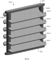
- the plasma process system also includes an exhaust baffle assembly positioned within the exhaust channel.
- the exhaust baffle assembly includes at least one baffle member shaped to deflect the flow of process exhaust gas within the exhaust channel. An outer surface of the at least one baffle member is conditioned to promote adherence of plasma process byproduct material present within the flow of process exhaust gas to the at least one baffle member.
- a method for plasma processing of a substrate.
- the method includes having a plasma process system that includes a plasma process chamber and an exhaust channel for the plasma process chamber.
- the plasma process chamber includes a plasma processing region in which a plasma is generated during operation of the plasma process chamber.
- the exhaust channel is fluidly connected to the plasma processing region.
- the exhaust channel is configured to direct a flow of process exhaust gas from the plasma processing region.
- the plasma process system also includes a pump connected to the exhaust channel.
- the pump is configured to apply a negative pressure to an interior of the exhaust channel.
- the plasma process system includes an exhaust baffle assembly positioned within the exhaust channel.
- the exhaust baffle assembly includes at least one baffle member shaped to deflect the flow of process exhaust gas within the exhaust channel.
- An outer surface of the at least one baffle member is conditioned to promote adherence of plasma process byproduct material present within the flow of process exhaust gas to the at least one baffle member.
- the method also includes generating a plasma in the plasma processing region in exposure to a substrate.
- the method also includes operating the pump to apply the negative pressure to the interior of the exhaust channel to draw the flow of process exhaust gas from the plasma processing region into the exhaust channel and through the exhaust baffle assembly within the exhaust channel.
- a method for manufacturing an exhaust baffle assembly for use in a plasma process system.
- the method includes forming at least one baffle member to fit within an exhaust channel of a plasma process chamber.
- the at least one baffle member is shaped to deflect a flow of process exhaust gas when positioned within the exhaust channel.
- the method also includes conditioning an outer surface of the at least one baffle member to promote adherence of plasma process byproduct material present within the flow of process exhaust gas to the at least one baffle member.
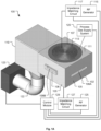
- Figure 1A shows an example system 100 for performing a plasma process on a substrate 101, in accordance with some embodiments.
- Figure 1B shows a vertical cross-section view through of a portion of the system 100, in accordance with some embodiments.
- the substrate 101 as referred to herein is a semiconductor wafer.
- the substrate 101 as referred to herein can be a substrate formed of sapphire, GaN, GaAs or SiC, or other substrate materials, and can include glass panels/substrates, metal foils, metal sheets, polymer materials, or the like.
- the substrate 101 as referred to herein may vary in form, shape, and/or size.
- the substrate 101 may correspond to a 200 mm (millimeters) semiconductor wafer, a 300 mm semiconductor wafer, or a 450 mm semiconductor wafer.
- the substrate 101 may correspond to a non-circular substrate, such as a rectangular substrate for a flat panel display, or the like, among other shapes.
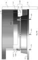
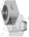
- the system 100 includes a plasma process chamber 102 for performing a plasma-based process on the substrate 101.
- the plasma-based process can be essentially any process in which constituents of a plasma are used to modify characteristics of the substrate 101 in a prescribed and controlled manner.
- the plasma-based process is an etching process to remove material from the substrate 101, or a deposition process to add material to the substrate 101, or a combination of etching and deposition processes.
- the chamber 102 includes walls 105 that enclose an interior of the chamber 102.
- the walls 105 are formed of an electrically conductive material and have an electrical connection to a reference ground potential.
- the walls 105 can include a number of openings/ports configured for various purposes.
- walls 105 of the example chamber 102 include an opening 106A for transfer of the substrate 101 into and out of the chamber 102.
- the opening 106A interfaces with a slit-valve that provides for passage of a robotic substrate handling device into the chamber 102 through the opening 106A and that provides for sealing of the opening 106A when the chamber 102 is in operation.
- the walls 105 of the example chamber 102 include an opening 106B that provides a viewport for viewing of a plasma processing region 109 within the chamber 102 either manually or by various equipment, such as an optical monitoring device or optical endpoint detection device, among other devices.
- the opening 106B can be covered in a sealed manner by a window 108 formed of an optically transparent material, such as glass or plastic, or other similar material.
- a substrate support structure 103 is present within the interior of the chamber 102 and is configured to hold the substrate 101 during performance of a plasma process within the chamber 102.
- the substrate support structure 103 is an electrostatic chuck configured to generate an electrostatic field that holds the substrate 101.
- the substrate support structure 103 can include various components and systems.
- the substrate support structure 103 can be configured to include one or more electrodes for transmission of radiofrequency power and/or for generation of bias voltage.
- the substrate support structure 103 can include one or more temperature control devices, such as heaters and/or cooling channels.
- the substrate support structure 103 can include a number of lifting pins and associated mechanics to facilitate movement of the substrate 101 between a robotic handling device and the substrate support structure 103.
- the substrate support structure 103 can include a number of sensors and/or probes for measuring temperature and for measuring electrical parameters, such as voltage and/or current.
- a top window structure 107 is positioned above the substrate support structure 103 and separated from the substrate support structure 103 such that the plasma processing region 109 is present between the substrate support structure 103 and the top window structure 107.
- the walls 105 include an upper flange structure 111 configured to receive and support the top window structure 107.
- the top window structure 107 is formed of a material through which radiofrequency (RF) signals can be transmitted, such as quartz or ceramic, among others.
- RF radiofrequency
- the top window structure 107 is configured to function as a gas distribution plate.
- the top window structure 107 can include a number of gas input ports, an arrangement of internal fluid channels fluidly connected to the gas input ports, and a number of gas output ports fluidly connected to the internal fluid channels.
- Process gas(es) supplied to the gas input ports of the top window structure 107 are flowed through the internal fluid channels to the gas output ports of the top window structure 107 where the process gas(es) are dispensed into the plasma processing region 109.
- the gas output ports and internal fluid channels of the top window structure 107 can be configured to dispense process gas(es) into the plasma processing region 109 in a spatially controlled manner.
- a coil assembly 113 is positioned above the top window structure 107.
- the coil assembly 113 is connected to a radiofrequency (RF) generator 115 through an impedance matching circuit 117.
- the coil assembly 113 is configured to transmit RF power through the top window structure 107 to the plasma processing region 109 when RF power is transmitted to the coil assembly 113 from the RF generator 115 by way of the impedance matching circuit 117.
- the impedance matching circuit 117 includes an arrangement of capacitors and inductors configured to ensure that an impedance seen by the RF generator 115 at the input of the impedance matching circuit 117 is sufficiently close to an output impedance for which the RF generator 115 is designed to operate (usually 50 Ohm), so that RF power generated and transmitted by the RF generator 115 will be transmitted into the plasma processing region 109 in an efficient manner, e.g., without unacceptable or undesirable reflection.
- the RF generator 115 can include one or more RF signal generators operating at one or more frequencies. Multiple RF signal frequencies can be supplied to the coil assembly 113 at the same time. In some embodiments, signal frequencies output by the RF generator 115 are set within a range extending from 1 kHz (kiloHertz) to 100 MHz (megaHertz). In some embodiments, signal frequencies output by the RF generator 115 are set within a range extending from 400 kHz to 60 MHz. In some embodiments, the RF generator 115 is set to generate RF signals at frequencies of 2 MHz, 27 MHz, 13.56 MHz, and 60 MHz.
- the RF generator 115 is set to generate one or more high frequency RF signals within a frequency range extending from about 2 MHz to about 60 MHz, and generate one or more low frequency RF signals within a frequency range extending from about 100 kHz to about 2 MHz. It should be understood that the above-mentioned RF signal frequency ranges are provided by way of example. In practice, the RF generator 115 can be configured to generate essentially any RF signal having essentially any frequency as needed to generate the plasma within the plasma processing region 109. Additionally, the RF generator 115 can include frequency-based filtering, i.e., high-pass filtering and/or low-pass filtering, to ensure that specified RF signal frequencies are transmitted to the coil assembly 113.
- frequency-based filtering i.e., high-pass filtering and/or low-pass filtering
- the process gas supply system 120 operates to deliver the one or more process gas(es) to the plasma processing region 109, and RF power is delivered from the RF generator 115 to the coil assembly 113, such that the RF power generates an electromagnetic field within the plasma processing region 109 so as to transform the one or more process gas(es) within the plasma processing region 109 into the plasma. Then, reactive constituents of the plasma, such as ions and/or radicals, can interact with portions of the substrate 101.
- a media blasting process can be performed (or reperformed) on the component to both clean the component and re-roughen/re-texture the exterior surface of the component.
- the ability to refurbish components by media blasting without recoating of the component avoids the expense of having to apply the coating to the component, and avoids generation of coating-induced stresses in the component that could lead to mechanical failure of the component.
- components can be refurbished many times, e.g., twenty or more times, by the media blasting process without compromising the mechanical integrity of the component through removal of too much component material.
- the at least one roughened surface can be formed at least in part by performing a knurling process on the ceramic component prior to firing of the ceramic component.
- the region of the bottom surface 107A inside of the outer peripheral ring-shaped area 107D is the at least one roughened surface 107C that is roughened/textured to have a surface roughness average (Ra) within a range extending from about 150 microinches to about 500 microinches (3.8 ⁇ m to about 12.7 ⁇ m). In some embodiments, the at least one roughened surface 107C is roughened/textured to have a surface roughness average (Ra) of about 500 microinches (12.7 ⁇ m). In some embodiments, the top window structure 107 remains in the form of an uncoated, bare ceramic component after formation of the at least one roughened surface 107C on the bottom surface 107A and during use of the top window structure 107 within the chamber 102.
- the above-mentioned surface-textured plasma process chamber component is the liner structure 139.
- Figure 3 shows an isometric view of the liner structure 139, in accordance with some embodiments.
- the liner structure 139 is configured to extend around at least a portion of a plasma processing region 109 within the chamber 102.
- the liner structure 139 has an inner surface 139A that is the at least one roughened surface oriented to be in exposure to plasma process byproduct material when the liner structure 139 is placed within the chamber 102 during operation of the chamber 102.
- an entirety of the liner structure 139, including the inner surface 139A and an outer surface 139B is roughened/textured to promote adherence of the plasma process byproduct material to the liner structure 139.
- the liner structure 139 is roughened/textured to have a surface roughness average (Ra) within a range extending from about 150 microinches to about 500 microinches (3.8 ⁇ m to about 12.7 ⁇ m). In some embodiments, the liner structure 139 is roughened/textured to have a surface roughness average (Ra) of about 500 microinches (12.7 ⁇ m).
- the above-mentioned surface-textured plasma process chamber component is a ring structure for installation within the chamber 102, where the ring structure is configured to circumscribe the substrate support structure 103 within the chamber 102.
- the ring structure can be one or both of the focus ring structure 135 and the edge ring structure 131, by way of example.
- the ring structure is characterized by having at least one process-exposed surface that is one or both of an inner surface of the ring structure and an upper surface of the ring structure.
- the at least one process-exposed surface is the at least one roughened surface oriented to be in exposure to plasma process byproduct material when the ring structure is placed within the chamber 102 during operation of the chamber 102.
- the process-exposed surface 131A of the edge ring structure 131 is roughened/textured to have a surface roughness average (Ra) within a range extending from about 150 microinches to about 500 microinches (3.8 ⁇ m to about 12.7 ⁇ m). In some embodiments, the process-exposed surface 131A of the edge ring structure 131 is roughened/textured to have a surface roughness average (Ra) of about 500 microinches (12.7 ⁇ m). .
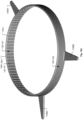
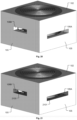
- Figure 5 shows an isometric view of the focus ring structure 135, in accordance with some embodiments.
- an inner surface 135A1 of the ring portion 135A of the focus ring structure 135 is the at least one roughened surface oriented to be in exposure to plasma process byproduct material when the focus ring structure 135 is placed within the chamber 102 during operation of the chamber 102.
- the top surfaces of the radial extension structures 135B1, 135B2, 135B3 are also some of the at least one roughened surface oriented to be in exposure to plasma process byproduct material when the focus ring structure 135 is placed within the chamber 102 during operation of the chamber 102.
- an entire outer surface of the focus ring structure 135, including the ring structure 135A and the radial extension structures 135B1, 135B2, 135B3 constitutes the at least one roughened surface oriented to be in exposure to plasma process byproduct material when the focus ring structure 135 is placed within the chamber 102 during operation of the chamber 102.
- the process-exposed surface(s) of the focus ring structure 135 is roughened/textured to have a surface roughness average (Ra) within a range extending from about 150 microinches to about 500 microinches (3.8 ⁇ m to about 12.7 ⁇ m). In some embodiments, the process-exposed surface(s) of the focus ring structure 135 is roughened/textured to have a surface roughness average (Ra) of about 500 microinches (12.7 ⁇ m).
- the process-exposed surfaces 133A, 133B, 133C of the ground ring structure 133 is roughened/textured to have a surface roughness average (Ra) within a range extending from about 150 microinches to about 500 microinches (3.8 ⁇ m to about 12.7 ⁇ m). In some embodiments, the process-exposed surfaces 133A, 133B, 133C of the ground ring structure 133 is roughened/textured to have a surface roughness average (Ra) of about 500 microinches (12.7 ⁇ m).
- the process-exposed surfaces 133A, 133B, 133C of the ground ring structure 133 are left uncoated after being subjected to the roughening/texturizing process and during use of the ground ring structure 133 within the chamber 102.
- the process-exposed surfaces 133A, 133B, 133C of the ground ring structure 133 are coated after being subjected to the roughening/texturizing process, and the coated ground ring structure 133 is then used within the chamber 102.
- the roughening/texturizing of the process-exposed surfaces 133A, 133B, 133C that is performed prior to coating can be defined to ensure that a prescribed amount of surface average roughness (Ra) remains on the process-exposed surfaces 133A, 133B, 133C after coating.
- the coating applied to the roughened/texturized process-exposed surfaces 133A, 133B, 133C of the ground ring structure 133 is either a yttria coating, or an anodization coating, or another type of coating that is chemically, mechanically, thermally, and electrically compatible with the plasma process performed within the chamber 102.
- the embodiments disclosed herein include that of a plasma process chamber, e.g., chamber 102, that includes one or more components having at least one process-exposed surface configured to have a surface roughness/texture that promotes adherence of plasma process byproduct material to the process-exposed surface. Also, it should be understood that the embodiments disclosed herein include operation of the plasma process chamber, that includes the one or more components with roughened/texturized process-exposed surfaces, in a plasma process operation that generates non-volatile and/or low-volatility byproduct materials.
- Figure 7 shows a flowchart of a method for plasma processing of a substrate, in accordance with some embodiments.
- the method includes an operation 701 for having a plasma process chamber, i.e., chamber 102, that includes the substrate support structure 103 and the top window structure 107.
- the substrate support structure 103 is configured to hold the substrate 101 in exposure to a plasma to be generated within the plasma processing region 109.
- the top window structure 107 is positioned above the substrate support structure 103 to establish the plasma processing region 109 between the substrate support structure 103 and the top window structure 107.
- the top window structure 107 is formed of ceramic material and has the bottom surface 107A facing the plasma processing region 109.
- the top window structure 107 is formed of aluminum oxide, silicon carbide, or of another ceramic material that is chemically, mechanically, thermally, and electrically compatible with operation of the chamber 102.
- the bottom surface 107A of the top window structure 107 has a surface roughness/texture that promotes adherence of plasma process byproduct material to the bottom surface 107A.
- the bottom surface 107A of the top window structure 107 has a surface roughness average (Ra) within a range extending from about 150 microinches to about 500 microinches (3.8 ⁇ m to about 12.7 ⁇ m).
- the bottom surface 107A of the top window structure 107 has a surface roughness average (Ra) of about 500 microinches (12.7 ⁇ m).
- the bottom surface 107A of the top window structure 107 has a surface roughness average (Ra) greater than 500 microinches.
- the bare ceramic material that forms the top window structure 107 is exposed at the bottom surface 107A of the top window structure 107.
- the method also includes an operation 703 for generating the plasma in the plasma processing region 109, such that constituents of the plasma interacting with a material on the substrate 101 to generate plasma process byproduct material, and where some of the plasma process byproduct material adheres to the bottom surface 107A of the top window structure 107.
- the material on the substrate 101 is a lead zirconate titanate (PZT) film.
- the material on the substrate 101 is a platinum (Pt) film.
- the material on the substrate 101 is a film that causes heavy byproduct deposition within the chamber 102 when exposed to the plasma generated in operation 703.
- generating the plasma in the operation 703 can include applying radiofrequency power to a process gas within the plasma processing region 109.
- the applied radiofrequency power can be within a range extending from about 400 Watts (W) to about 1250 W. However, it should be understood that in various embodiments the applied radiofrequency power can be less than 400 W or greater than 1250 W.
- the radiofrequency power is applied by radiofrequency signals having a frequency of about 13.56 MHz. However, it should be understood that in various embodiments the radiofrequency power can be applied by radiofrequency signals having a frequency other than 13.56 MHz.
- the method can include an operation for generating a bias voltage at the substrate support structure 103.
- the bias voltage is generated within a range extending from about 100 Volts (V) to about 600 V. However, it should be understood that in various embodiments the bias voltage can be less than 100 V or greater than 600 V. Also, in some embodiments, the bias voltage can be generated by radiofrequency signals having a frequency of about 13.56 MHz. However, it should be understood that in various embodiments the bias voltage can be generated by radiofrequency signals having a frequency other than 13.56 MHz. Also, in various embodiments, the bias voltage can be generated by a direct current source.
- the method can include an operation for maintaining a temperature of the substrate support structure 103 within a range extending from about 40° Celsius (C) to about 100° C. However, it should be understood that in various embodiments the temperature of the substrate support structure 103 can be maintained at less than 40° C or greater than 100° C. Also, in some embodiments, the method can include an operation for maintaining a pressure within the plasma processing region 109 within a range extending from about 5 milliTorr to about 50 milliTorr. However, it should be understood that in various embodiments the pressure within the plasma processing region 109 can be maintained at less that 5 milliTorr or greater than 50 milliTorr.
- generating the plasma in the operation 703 includes supplying process gas to the plasma processing region 109, where the process gas is one or more of chlorine (Cl 2 ), boron trichloride (BCl 3 ), argon (Ar), carbon tetrafluoride (CF 4 ), oxygen (O 2 ), trifluoromethane (CHF 3 ), and sulfur hexafluoride (SF 6 ).
- the process gas is one or more of chlorine (Cl 2 ), boron trichloride (BCl 3 ), argon (Ar), carbon tetrafluoride (CF 4 ), oxygen (O 2 ), trifluoromethane (CHF 3 ), and sulfur hexafluoride (SF 6 ).
- generating the plasma in the operation 703 includes supplying chlorine (Cl 2 ) to the plasma processing region 109 at a flow rate within a range extending from about 20 standard cubic centimeters per minute (sccm) to about 300 sccm.
- generating the plasma in the operation 703 includes supplying boron trichloride (BCl 3 ) to the plasma processing region 109 at a flow rate within a range extending from about 50 sccm to about 300 sccm. In some embodiments, generating the plasma in the operation 703 includes supplying argon (Ar) to the plasma processing region 109 at a flow rate within a range extending from about 50 sccm to about 300 sccm. In some embodiments, generating the plasma in the operation 703 includes supplying carbon tetrafluoride (CF 4 ) to the plasma processing region 109 at a flow rate within a range extending from about 50 sccm to about 200 sccm.
- BCl 3 boron trichloride
- generating the plasma in the operation 703 includes supplying argon (Ar) to the plasma processing region 109 at a flow rate within a range extending from about 50 sccm to about 300 sccm.
- generating the plasma in the operation 703 includes supplying oxygen (O 2 ) to the plasma processing region 109 at a flow rate within a range extending from about 20 sccm to about 300 sccm. In some embodiments, generating the plasma in the operation 703 includes supplying trifluoromethane (CHF 3 ) to the plasma processing region 109 at a flow rate within a range extending from about 50 sccm to about 300 sccm. In some embodiments, generating the plasma in the operation 703 includes supplying sulfur hexafluoride (SF 6 ) to the plasma processing region 109 at a flow rate within a range extending from about 50 sccm to about 300 sccm.
- oxygen oxygen
- generating the plasma in the operation 703 includes supplying trifluoromethane (CHF 3 ) to the plasma processing region 109 at a flow rate within a range extending from about 50 sccm to about 300 sccm.
- CHF 3 triflu
- the method for plasma processing of the substrate as shown in Figure 7 can also include using the liner structure 139 within the chamber 102, where the liner structure 139 is configured to extend around at least a portion of the plasma processing region 109 within the chamber 102.
- the liner structure 139 has the inner surface 139A that is oriented to be in exposure to the plasma process byproduct material.
- the inner surface 139A of the liner structure 139 has a surface roughness that promotes adherence of the plasma process byproduct material to the inner surface 139A of the liner structure 139.
- the liner structure 139 is formed of aluminum oxide, silicon carbide, or of another ceramic material that is chemically, mechanically, thermally, and electrically compatible with operation of the chamber 102.
- the inner surface 139A of the liner structure 139 has a surface roughness average (Ra) within a range extending from about 150 microinches to about 500 microinches (3.8 ⁇ m to about 12.7 ⁇ m). In some embodiments, the inner surface 139A of the liner structure 139 has a surface roughness average (Ra) of about 500 microinches ( ⁇ m). In some embodiments, the inner surface 139A of the liner structure 139 has a surface roughness average (Ra) greater than 500 microinches (12.7 ⁇ m). In some embodiments, the bare ceramic material that forms the liner structure 139 is exposed at the inner surface 139A of the liner structure 139.
- Ra surface roughness average
- non-coated ceramic liner structure 139 having an engineered surface roughness/texture that enables and promotes adherence of the plasma process byproduct material eliminates the difficulty and expense of having to refurbish a coated liner structure, such as hard anodized aluminum liner structure that has a yttria coating.
- non-coated ceramic liner structure 139 having an engineered surface roughness/texture that enables and promotes adherence of the plasma process byproduct material extends the lifetime of the liner structure 139 by eliminating the increased risk of mechanical failure that may be caused by stresses induced within the liner structure 139 during refurbishment and recoating processes, such as occur during the refurbishment and recoating processes used in conjunction with a hard anodized aluminum chamber liner structure having a yttria coating.
- the method for plasma processing of the substrate as shown in Figure 7 can also include using a ring structure within the chamber 102, where the ring structure is configured to circumscribe the substrate support structure 103 within the chamber 102.
- the ring structure has at least one process-exposed surface that is one or both of an inner surface and an upper surface of the ring structure.
- the process-exposed surface is oriented to be in exposure to the plasma process byproduct material.
- the process-exposed surface of the ring structure has a surface roughness that enables and promotes adherence of the plasma process byproduct material to the process-exposed surface of the ring structure.
- the ring structure is the focus ring structure 135.
- the ring structure is the edge ring structure 131.
- the ring structure is the ground ring structure 133.
- the ring structure is formed of aluminum oxide, silicon carbide, or of another ceramic material that is chemically, mechanically, thermally, and electrically compatible with operation of the chamber 102.
- the ring structure is formed of ceramic material, a bare ceramic material of which the ring structure is formed is exposed at the roughened/texturized process-exposed surface of the ring structure.
- the ring structure is formed of an electrically conductive material, such as aluminum or stainless steel or another metallic material that is chemically, mechanically, thermally, and electrically compatible with operation of the chamber 102.
- the roughened/texturized process-exposed surface of the ring structure may remain uncoated when used in the chamber 102.
- the roughened/texturized process-exposed surface of the ring structure may be coated when used in the chamber 102.
- the coating applied to the electrically conductive ring structure is a yttria coating, or an anodization, or another type of coating that is chemically, mechanically, thermally, and electrically compatible with operation of the chamber 102.
- the process-exposed surface of the ring structure has a surface roughness average (Ra) within a range extending from about 150 microinches to about 500 microinches (3.8 ⁇ m to about 12.7 ⁇ m). In some embodiments, the process-exposed surface of the ring structure has a surface roughness average (Ra) of about 500 microinches (12.7 ⁇ m). In some embodiments, the process-exposed surface of the ring structure has a surface roughness average (Ra) greater than 500 microinches (12.7 ⁇ m).
- FIG. 8 shows a flowchart of a method for manufacturing a surface-textured plasma process chamber component, in accordance with some embodiments.
- the method includes an operation 801 for forming a ceramic component for installation within a plasma process chamber, e.g., within the chamber 102, where the ceramic component has at least one process-exposed surface.
- the ceramic component is formed of aluminum oxide, silicon carbide, or of another ceramic material that is chemically, mechanically, thermally, and electrically compatible with operation of the chamber 102.
- the ceramic component is either the top window structure 107, the liner structure 139, the focus ring structure 135, or the edge ring structure 131.
- the method also includes an operation 803 for roughening the at least one process-exposed surface to have a surface roughness that promotes adhesion of plasma process byproduct material to the at least one process-exposed surface.
- the operation 803 is performed to impart a surface roughness average (Ra) within a range extending from about 150 microinches to about 500 microinches (3.8 ⁇ m to about 12.7 ⁇ m) to the at least one process-exposed surface of the ceramic component.
- the operation 803 is performed to impart a surface roughness average (Ra) greater than 500 microinches (12.7 ⁇ m). to the at least one process-exposed surface of the ceramic component.
- the operation 803 for roughening the at least one process-exposed surface is done by a media blasting process.
- the media blasting process impacts the at least one process-exposed surface with media including one or more of aluminum oxide, silicon carbide, crushed glass grit, glass beads, ceramic, glass, walnut shell, pumice, steel grit, steel shot, aluminum shot, zinc shot, copper shot, cut wire, garnet, silica sand, and staurolite.
- the operation 801 for forming the ceramic component includes performing a knurling process on the ceramic component prior to firing of the ceramic component, where the knurling process is defined to impart texture to the at least one process-exposed surface of the ceramic component.
- a bare ceramic material of which the ceramic component is formed is exposed at the at least one process-exposed surface after roughening of the at least one process-exposed surface in the operation 803.
- FIG. 9 shows a flowchart of a method for converting a coated plasma process chamber component into a surface-textured plasma process chamber component, in accordance with some embodiments.
- the method includes an operation 901 for stripping a coating from a ceramic component down to a bare ceramic material of which the ceramic component is formed.
- the ceramic component is configured for installation within a plasma process chamber, e.g., within the chamber 102. Also, the ceramic component has at least one process-exposed surface.
- the ceramic component is formed of aluminum oxide, silicon carbide, or of another ceramic material that is chemically, mechanically, thermally, and electrically compatible with operation of the chamber 102.
- the ceramic component is either the top window structure 107, the liner structure 139, the focus ring structure 135, or the edge ring structure 131.
- the method also includes an operation 903 for roughening the at least one process-exposed surface of the ceramic component to have a surface roughness that promotes adhesion of plasma process byproduct material to the at least one process-exposed surface.
- the operation 903 is performed to impart a surface roughness average (Ra) within a range extending from about 150 microinches to about 500 microinches (3.8 ⁇ m to about 12.7 ⁇ m) to the at least one process-exposed surface of the ceramic component.
- the operation 903 is performed to impart a surface roughness average (Ra) greater than 500 microinches (12.7 ⁇ m) to the at least one process-exposed surface of the ceramic component.
- the operation 903 for roughening the at least one process-exposed surface is done by a media blasting process.
- the media blasting process impacts the at least one process-exposed surface with media including one or more of aluminum oxide, silicon carbide, crushed glass grit, glass beads, ceramic, glass, walnut shell, pumice, steel grit, steel shot, aluminum shot, zinc shot, copper shot, cut wire, garnet, silica sand, and staurolite.
- a bare ceramic material of which the ceramic component is formed is exposed at the at least one process-exposed surface after roughening of the at least one process-exposed surface in the operation 903.
- the operation 901 for stripping the coating from the ceramic component is done using a media blasting process. And, in some embodiments, both of operations 901 and 903 are performed simultaneously using a same media blasting process.
- the focus ring structure 135 Prior to the surface roughening/texturizing embodiments disclosed herein, the focus ring structure 135 has conventionally been formed to have a relatively smooth, featureless surface on both the inner and outer surfaces of the ring portion 135A and on the radial extension structures 135B1, 135B2, 135B3. Plasma process byproduct materials that are non-volatile and/or have low-volatility adhere poorly to smooth, featureless surfaces. For example, in plasma-based etching of PZT film or Pt film on the substrate 101, significant amounts of non-volatile and/or low-volatility etch byproduct materials are generated and can have poor adhesion to the focus ring structure 135 that is conventionally formed to have smooth, featureless surfaces.
- the plasma process byproduct materials build up on the focus ring structure 135 they can flake off and/or peel off and land on the substrate 101 and/or substrate support structure 103 due to the close proximity of the focus ring structure 135 to both the substrate 101 and the substrate support structure 103. Having plasma process byproduct material landing on the substrate 101 can damage the substrate 101 or cause formation of defects in the structures being formed on the substrate 101.
- having plasma process byproduct material landing on the substrate support structure 103 can interfere with proper clamping of the substrate 101 on the substrate support structure 103 and can cause adversely high helium flow at the backside of the substrate 101, i.e., from the region between the substrate 101 and the substrate support structure 103, any of which can lead to formation of defects on the substrate 101.
- the roughening/texturizing of the surface of the focus ring structure 135 can promote and substantially improve adhesion of plasma process byproduct materials to the focus ring structure 135, so as to accommodate a greater build up of plasma process byproduct material on the focus ring structure 135 before flaking-off and/or peeling-off of plasma process byproduct material from the focus ring structure 135 occurs. Therefore, roughening/texturizing of the surface of the focus ring structure 135 serves to delay the onset of flaking-off and/or peeling-off of plasma process byproduct material from the focus ring structure 135. However, continuing to further increase the roughness/texture of the focus ring structure 135 may have a diminishing effect on increasing the mean time until flaking-off and/or peeling-off of plasma process byproduct material from the focus ring structure 135 occurs.
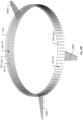
- Figure 10A shows an isometric view of a focus ring structure 135-1 that has a controlled surface topographical variation on an inner surface 135-1A1 of a ring portion 135-1A of the focus ring structure 135-1 to promote adherence of the plasma process byproduct material to the focus ring structure 135-1, in accordance with some embodiments.
- the focus ring structure 135-1 includes a ring portion 135-1A and the three radial extension structures 135B1, 135B2, 135B3.
- the ring portion 135-1A is configured as a right circular hollow cylinder to circumscribe the substrate support structure 103 within the chamber 102.
- the radial extension structures 135B1, 135B2, 135B3 are configured to extend radially outward from an outer surface 135-1A2 of the ring portion 135-1A.
- the radial extension structures 135B1, 135B2, 135B3 are configured to engage with the three respective lifting components 137A, 137B, 137C to enable raising and lowering of the focus ring structure 135-1 relative to the substrate support structure 103.
- the focus ring structure 135-1 is formed of ceramic material.
- the focus ring structure 135 can be formed of aluminum oxide, silicon carbide, or essentially any other ceramic material that is chemically, mechanically, thermally, and electrically compatible for service as the focus ring structure 135 during operation of the chamber 102.
- Figure 10B shows how the lattice pattern of the convex structures 1001 extends around the full circumference of the inner surface 135-1A1 of the ring portion 135-1A of the focus ring structure 135-1.
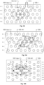
- Figure 10C shows a top view of the focus ring structure 135-1 of Figure 10A , in accordance with some embodiments.
- Figure 10D shows a detailed view 1003 as referenced in Figure 10C , in accordance with some embodiments.
- the convex structures 1001 are formed to have a dome shape.
- FIG. 10E shows a cross-section view through two adjacent convex structures 1001, in accordance with some embodiments.
- each convex structure 1001 extends inward toward the area circumscribed by the ring portion 135-1A of the focus ring structure 135-1 by a distance (d1) within a range extending from about 0.5 millimeter (mm) to about 2 mm, or within a range extending from about 1 mm to about 2 mm, or of about 1 mm.
- a distance (d2) between adjacent convex structures 1001 is within a range extending from about 0.5 mm to about 2 mm.
- the distance (d2) between adjacent convex structures 1001 is about 1 mm.
- Figure 10F shows a vertical cross-section through a center of the focus ring structure 135-1, in accordance with some embodiments.
- the convex structures 1001 are arranged in a rectangular lattice that includes five rows. In other embodiments, the convex structures 1001 can be arranged in a rectangular lattice that includes either less than five rows or more than five rows.
- Figure 10G shows a diagram for forming the convex structures 1001 in a rectangular lattice over the inner surface 135-1A1 of the ring portion 135-1A of the focus ring structure 135-1, in accordance with some embodiments.
- the rectangular lattice is characterized has having the convex structures 1001 positioned in a repeating rectangular pattern, as indicated by the rectangles 1005, in both a horizontal direction (x) around the circumference of the inner surface 135-1A1 of the ring portion 135-1A of the focus ring structure 135-1, and in a vertical direction (y).
- the convex structures 1001 are spaced apart in the horizontal direction (x) by a distance 1007, and are spaced apart in the vertical direction (y) by a distance 1009, where the distance 1007 is greater than the distance 1009.
- the distances 1007 and 1009 are within a range extending from about 0.5 mm to about 2 mm.
- the distance 1009 is about 1 mm.
- the rectangular lattice of convex structures 1001 has five rows (R1 through R5). However, it should be understood that in various embodiments the rectangular lattice of convex structures 1001 can have two or more rows.
- the convex structure 1001 can be arranged over the inner surface 135-1A1 of the ring portion 135-1A of the focus ring structure 135-1 in either a square lattice, a hexagonal lattice, a parallelogrammic lattice, or a rhombic lattice.
- Figure 10H shows a diagram for forming the convex structures 1001 in a square lattice over the inner surface 135-1A1 of the ring portion 135-1A of the focus ring structure 135-1, in accordance with some embodiments.
- the square lattice is characterized has having the convex structures 1001 positioned in a repeating square pattern, as indicated by the squares 1011, in both the horizontal direction (x) around the circumference of the inner surface 135-1A1 of the ring portion 135-1A of the focus ring structure 135-1, and in the vertical direction (y).
- the convex structures 1001 are spaced apart in the horizontal direction (x) by a distance 1013, and are spaced apart in the vertical direction (y) by a distance 1015, where the distance 1013 is substantially equal to the distance 1015.
- the distances 1013 and 1015 are within a range extending from about 0.5 mm to about 2 mm.
- the distances 1013 and 1015 are about 1 mm.
- the square lattice of convex structures 1001 has five rows (R1 through R5). However, it should be understood that in various embodiments the square lattice of convex structures 1001 can have two or more rows.
- Figure 10I shows a diagram for forming the convex structures 1001 in a hexagonal lattice over the inner surface 135-1A1 of the ring portion 135-1A of the focus ring structure 135-1, in accordance with some embodiments.
- the hexagonal lattice is characterized has having the convex structures 1001 positioned in a repeating equilateral triangle pattern in both the horizontal direction (x) around the circumference of the inner surface 135-1A1 of the ring portion 135-1A of the focus ring structure 135-1 and in the vertical direction (y), with adjacent equilateral triangles of the pattern inverted in the vertical direction (y), as indicated by the equilateral triangles 1017.
- adjacent convex structures 1001 are spaced apart from each other by a distance 1019.
- the distance 1019 is within a range extending from about 0.5 mm to about 2 mm. In some embodiments, the distance 1019 is about 1 mm.
- the hexagonal lattice of convex structures 1001 has five rows (R1 through R5). However, it should be understood that in various embodiments the hexagonal lattice of convex structures 1001 can have two or more rows.
- Figure 10J shows a diagram for forming the convex structures 1001 in a parallelogrammic lattice over the inner surface 135-1A1 of the ring portion 135-1A of the focus ring structure 135-1, in accordance with some embodiments.
- the parallelogrammic lattice is characterized has having the convex structures 1001 positioned in a repeating parallelogram pattern in both the horizontal direction (x) around the circumference of the inner surface 135-1A1 of the ring portion 135-1A of the focus ring structure 135-1 and in the vertical direction (y), with adjacent parallelograms of the pattern having coincident vertices, as indicated by the parallelograms 1021.
- the parallelogram 1021 that defines the parallelogrammic lattice has two horizontal parallel sides of equal length 1023 oriented to extend substantially in the horizontal direction (x), and two skewed parallel sides of equal length 1025 oriented to extend at an angle 1027 between the two horizontal parallel sides.
- adjacent convex structures 1001 are spaced apart from each other by three distances 1029, 1031, 1033.
- the distances 1029, 1031, 1033 are within a range extending from about 0.5 mm to about 2 mm. In some embodiments, a smallest of the distances 1029, 1031, 1033 is about 1 mm.
- the parallelogrammic lattice of convex structures 1001 has five rows (R1 through R5). However, it should be understood that in various embodiments the parallelogrammic lattice of convex structures 1001 can have two or more rows.
- Figure 10K shows a diagram for forming the convex structures 1001 in a rhombic lattice over the inner surface 135-1A1 of the ring portion 135-1A of the focus ring structure 135-1, in accordance with some embodiments.
- the rhombic lattice is characterized has having the convex structures 1001 positioned in a repeating rhombus pattern, in both the horizontal direction (x) around the circumference of the inner surface 135-1A1 of the ring portion 135-1A of the focus ring structure 135-1 and in the vertical direction (y), with adjacent rhombuses of the pattern having coincident vertices, as indicated by the rhombuses 1035.
- the rhombus 1035 that defines the rhombic lattice is a parallelogram that has opposite equal acute angles 1037, and opposite equal obtuse angles 1039, and four sides of equal length 1041.
- adjacent convex structures 1001 are spaced apart from each other by two distances 1043 and 1045.
- the distances 1043 and 1045 are within a range extending from about 0.5 mm to about 2 mm.
- a smallest of the distances 1043 and 1045 is about 1 mm.
- the rhombic lattice of convex structures 1001 has nine rows (R1 through R9).
- the rhombus 1035 is configured such that convex structures 1001 in vertically adjacent ones of the rows, e.g., R1 through R9, do not overlap with each other in the vertical direction (y). However, in some embodiments, the rhombus 1035 is configured such that convex structures 1001 in vertically adjacent ones of the rows, e.g., R1 through R9, do have some amount of overlap with each other in the vertical direction (y). It should be understood that in various embodiments the rhombic lattice of convex structures 1001 can have three or more rows.
- the controlled surface topographical variation on the inner surface 135-1A1 of the ring portion 135-1A of the focus ring structure 135-1 is formed by a media blasting process.
- a protective mask is applied to the inner surface 135-1A1 of the ring portion 135-1A of the focus ring structure 135-1 to cover the locations where the convex structures 1001 are to be formed.
- the inner surface 135-1A1 of the ring portion 135-1A of the focus ring structure 135-1 is subjected to the media blasting process to remove, i.e., erode, a layer of ceramic material of which the focus ring structure 135-1 is formed from the inner surface 135-1A1, thereby forming the convex structures 1001 on the inner surface 135-1A1.
- the protective mask is removed.
- the media blasting process used to form the convex structures 1001 simultaneously roughens/texturizes the portions of the inner surface 135-1A1 between and around the convex structures 1001 to promote adherence of plasma process byproduct material to the inner surface 135-1A1.
- the media used in the media blasting process to form the convex structures 1001 can include one or more of aluminum oxide, silicon carbide, crushed glass grit, glass beads, ceramic, glass, walnut shell, pumice, steel grit, steel shot, aluminum shot, zinc shot, copper shot, cut wire, garnet, silica sand, and staurolite, among other types of media.
- surfaces of the focus ring structure 135-1 beyond the inner surface 135-1A1 can be subjected to the media blasting process to receive a prescribed surface roughness average (Ra).
- an entirety of the ring portion 135-1A and the top surfaces of the radial extension structures 135B1, 135B2, 135B3 can be subjected to the media blasting process to receive a prescribed surface roughness average (Ra) within a range extending from about 150 microinches to about 500 microinches (3.8 ⁇ m to about 12.7 ⁇ m).
- Ra surface roughness average
- the convex structures 1001 can be formed by performing a knurling process on the inner surface 135-1A1 of the ring portion 135-1A of the focus ring structure 135-1 when the ceramic material of the focus ring structure 135-1 is in a soft green state before firing of the ceramic.
- the knurling process is a manufacturing process in which a pattern of some depth is formed within a material in a soft malleable state. After the knurling and firing of the ceramic material of the focus ring structure 135-1, the convex structures 1001 will be present on the inner surface 135-1A1 of the ring portion 135-1A.
- the focus ring structures 135-1 can be subjected to the above-mentioned media blasting process to impart a prescribed surface roughness average (Ra) to the ring portion 135-1A and radial extension structures 135B1, 135B2, 135B3 of the focus ring structure 135-1.
- the convex structures 1001 and surface roughness average (Ra) imparted to the bare ceramic material of the focus ring structure 135-1 allows for use of the focus ring structure 135-1 within the chamber 102 in a bare, uncoated form, which eliminates the cost and risks associated with coating and re-coating of the focus ring structure 135-1.
- the arrangement of convex structures 1001 can be defined in a manner that increases a surface area of the inner surface 135-1A1 of the ring portion 135-1A by 400% or more, which provides a deliberate and highly contrasting surface topography upon which heavy plasma process byproduct material can deposit and adhere.
- the surface roughness average (Ra) imparted to the focus ring structure 135-1 by the media blasting process provides a robust, highly-textured surface for better adhesion of non-volatile and/or low-volatility plasma process by product material to the focus ring structure 135-1.
- the enhanced plasma process byproduct material adhesion and retention to the focus ring structure 135-1 provides for an increase in the mean time between cleaning (MTBC) of the chamber 102, which improves substrate 101 fabrication throughput.
- the ability to use the focus ring structure 135-1 within the chamber 102 as a bare, uncoated ceramic component extends the service lifetime of the focus ring structure 135-1 by eliminating the need to remove coating material from the focus ring structure 135-1 during refurbishment of the focus ring structure 135-1.
- FIG 11 shows a flowchart of a method for plasma processing of a substrate, in accordance with some embodiments.
- the method includes an operation 1101 for having a plasma process chamber, i.e., chamber 102, that includes the substrate support structure 103 and the focus ring structure 135-1.
- the focus ring structure 135-1 includes the ring portion 135-1A formed of ceramic material.
- the focus ring structure 135-1 is formed of aluminum oxide, silicon carbide, or of another ceramic material that is chemically, mechanically, thermally, and electrically compatible with operation of the chamber 102.
- the ring portion 135-1A is configured to circumscribe the substrate support structure 103 within the chamber 102.
- the ring portion 135-1A has the inner surface 135-1A1 oriented to be in exposure to the plasma processing region 109 in which plasma process byproduct material is generated during operation of the chamber 102.
- the inner surface 135-1A1 is formed to have a controlled surface topographical variation that promotes adherence of the plasma process byproduct material to the inner surface 135-1A1.
- the focus ring structure 135-1 has a surface roughness average (Ra) within a range extending from about 150 microinches to about 500 microinches (3.8 ⁇ m to about 12.7 ⁇ m). In some embodiments, the focus ring structure 135-1 has a surface roughness average (Ra) of about 500 microinches (12.7 ⁇ m).
- the bare ceramic material that forms the focus ring structure 135-1 is exposed at the exterior surface of the focus ring structure 135-1, and particularly at the inner surface 135-1A1 of the ring portion 135-1A of the focus ring structure 135-1.
- the method also includes an operation 1103 for generating the plasma in the plasma processing region 109, such that constituents of the plasma interact with a material on the substrate 101 to generate plasma process byproduct material, and where some of the plasma process byproduct material adheres to the focus ring structure 135-1.
- the material on the substrate 101 is a lead zirconate titanate (PZT) film.
- the material on the substrate 101 is a platinum (Pt) film.
- the material on the substrate 101 is a film that causes heavy byproduct deposition within the chamber 102 when exposed to the plasma generated in operation 1103.
- generating the plasma in the operation 1103 can include applying radiofrequency power to a process gas within the plasma processing region 109.
- the applied radiofrequency power can be within a range extending from about 400 W to about 1250 W. However, it should be understood that in various embodiments the applied radiofrequency power can be less than 400 W or greater than 1250 W.
- the radiofrequency power is applied by radiofrequency signals having a frequency of about 13.56 MHz. However, it should be understood that in various embodiments the radiofrequency power can be applied by radiofrequency signals having a frequency other than 13.56 MHz.
- the method can include an operation for generating a bias voltage at the substrate support structure 103.
- the bias voltage is generated within a range extending from about 100 V to about 600 V. However, it should be understood that in various embodiments the bias voltage can be less than 100 V or greater than 600 V. Also, in some embodiments, the bias voltage can be generated by radiofrequency signals having a frequency of about 13.56 MHz. However, it should be understood that in various embodiments the bias voltage can be generated by radiofrequency signals having a frequency other than 13.56 MHz. Also, in various embodiments, the bias voltage can be generated by a direct current source.
- the method can include an operation for maintaining a temperature of the substrate support structure 103 within a range extending from about 40° C to about 100° C. However, it should be understood that in various embodiments the temperature of the substrate support structure 103 can be maintained at less than 40° C or greater than 100° C. Also, in some embodiments, the method can include an operation for maintaining a pressure within the plasma processing region 109 within a range extending from about 5 milliTorr to about 50 milliTorr. However, it should be understood that in various embodiments the pressure within the plasma processing region 109 can be maintained at less that 5 milliTorr or greater than 50 milliTorr.
- generating the plasma in the operation 1103 includes supplying process gas to the plasma processing region 109, where the process gas is one or more of chlorine (Cl 2 ), boron trichloride (BCl 3 ), argon (Ar), carbon tetrafluoride (CF 4 ), oxygen (O 2 ), trifluoromethane (CHF 3 ), and sulfur hexafluoride (SF 6 ).
- the process gas is one or more of chlorine (Cl 2 ), boron trichloride (BCl 3 ), argon (Ar), carbon tetrafluoride (CF 4 ), oxygen (O 2 ), trifluoromethane (CHF 3 ), and sulfur hexafluoride (SF 6 ).
- generating the plasma in the operation 1103 includes supplying chlorine (Cl 2 ) to the plasma processing region 109 at a flow rate within a range extending from about 20 sccm to about 300 sccm.
- generating the plasma in the operation 1103 includes supplying boron trichloride (BCl 3 ) to the plasma processing region 109 at a flow rate within a range extending from about 50 sccm to about 300 sccm. In some embodiments, generating the plasma in the operation 1103 includes supplying argon (Ar) to the plasma processing region 109 at a flow rate within a range extending from about 50 sccm to about 300 sccm. In some embodiments, generating the plasma in the operation 1103 includes supplying carbon tetrafluoride (CF 4 ) to the plasma processing region 109 at a flow rate within a range extending from about 50 sccm to about 200 sccm.
- BCl 3 boron trichloride
- generating the plasma in the operation 1103 includes supplying argon (Ar) to the plasma processing region 109 at a flow rate within a range extending from about 50 sccm to about 300 sccm.
- generating the plasma in the operation 1103 includes supplying oxygen (O 2 ) to the plasma processing region 109 at a flow rate within a range extending from about 20 sccm to about 300 sccm. In some embodiments, generating the plasma in the operation 1103 includes supplying trifluoromethane (CHF 3 ) to the plasma processing region 109 at a flow rate within a range extending from about 50 sccm to about 300 sccm. In some embodiments, generating the plasma in the operation 1103 includes supplying sulfur hexafluoride (SF 6 ) to the plasma processing region 109 at a flow rate within a range extending from about 50 sccm to about 300 sccm.
- SF 6 sulfur hexafluoride
- FIG. 12 shows a flowchart of a method for manufacturing a focus ring structure for use in a plasma process chamber, in accordance with some embodiments.
- the method includes an operation 1201 for forming a ring structure of a ceramic material, such as the ring portion 135-1A of the focus ring structure 135-1, where the ring structure is configured to circumscribe a substrate support structure, e.g., the substrate support structure 103, within a plasma process chamber, e.g., within the chamber 102.
- the ring structure has an inner surface, e.g., the inner surface 135-1A1, oriented to be in exposure to a plasma processing region in which plasma process byproduct material is generated when the ring structure is placed within the plasma process chamber during operation of the plasma process chamber.
- the media blasting process impacts the inner surface of the ring structure with media including one or more of aluminum oxide, silicon carbide, crushed glass grit, glass beads, ceramic, glass, walnut shell, pumice, steel grit, steel shot, aluminum shot, zinc shot, copper shot, cut wire, garnet, silica sand, and staurolite, among others.
- the operation 1203 includes performing a knurling process on the inner surface of the ring structure prior to firing of the ceramic material of which the ring structure is formed.
- plasma process byproduct materials are free to move around in the chamber 102 in accordance with process gas flow patterns and/or existing pressure gradients.
- plasma processing operations that generate non-volatile and/or low volatility byproduct materials such as PZT etching processes or Pt etching processes, among others, it is possible for plasma process byproduct materials to travel into the opening 106A and to the access control device 1301.
- These plasma process byproduct materials can deposit on the chamber wall 105 within the opening 106A and on the inner surface(s) of the access control device 1301. Then, during subsequent operation of the access control device 1301 it is possible for some of the deposited plasma process byproduct materials to move into the access control device 1301 and possibly even into the substrate handling module 1303.
- FIG. 14 shows a substrate access port shield 1401 for use in the chamber 102, in accordance with some embodiments.
- the substrate access port shield 1401 includes a shield segment 1403 configured to be positioned over a portion of the opening 106A within the chamber 102.
- the substrate access port shield 1401 also includes a first support segment 1405 extending from a first end of the shield segment 1403.
- the substrate access port shield 1401 also includes a second support segment 1407 extending from a second end of the shield segment 1403.
- the shield segment 1403 and the first support segment 1405 and the second support segment 1407 form an integral shield structure that extends along an arc.
- the arc of the substrate access port shield 1401 is conformal with an arc of the liner structure 139.
- the cutout areas 1409A, 1409B, 1409C are also formed to enable the substrate access port shield 1401 to be held securely on the focus ring structure 135/135-1 by the force of gravity alone, i.e., without other fastening devices.
- one or more fastening devices can be used to affix the substrate access port shield 1401 to the focus ring structure 135/135-1.
- the substrate access port shield 1401 can include one or more additional cutout areas to accommodate viewing of the plasma processing region 109, such as for optical endpoint spectrometry (OES) purposes or other purposes, when the focus ring structure 135/135-1 is in the plasma processing position.
- OES optical endpoint spectrometry
- Figure 17A shows a side view of the example substrate access port shield 1401A positioned on the focus ring structure 135/135-1, with the focus ring structure 135/135-1 in the fully lowered position, in accordance with some embodiments.
- the vertical distance 1411 of the shield segment 1403A of the substrate access port shield 1401A covers about 75% of the vertical extent of the opening 106A when the focus ring structure 135/135-1 is in the fully lowered position.
- the substrate access port shield 1401A is configured to cover at least about 50% of the vertical extent of the opening 106A. In some embodiments, with substrate access port shield 1401A positioned on the focus ring structure 135/135-1 and with the focus ring structure 135/135-1 in the fully lowered position, the substrate access port shield 1401A is configured to cover at least about two-thirds of the vertical extent of the opening 106A.
- the vertical distance 1411 of the shield segment 1403A of the substrate access port shield 1401A can be defined so that the shield segment 1403A still covers a portion of the vertical extent of the opening 106A, so long as an unobscured vertical extent of the opening 106A is large enough to provide for interference-free movement of the substrate 101 and the robotic substrate handling device 1305 through the opening 106A.
- the substrate access port shield 1401/1401A is configured as a portion of a right circular hollow cylinder. In some embodiments, a radial thickness of the substrate access port shield 1401/1401A is substantially uniform. In various embodiments, a radial thickness of the substrate access port shield 1401/1401A is within a range extending from about 0.125 inches (3.175 mm) to about 0.5 inches (12.7 mm), or within a range extending from about 0.375 inches (9.525 mm) to about 0.5 inches (12.7 mm), or about 0.217 inches (5.512 mm) or about 0.375 inches (9.525 mm). In some embodiments, the radial thickness of the substrate access port shield 1401/1401A is non-uniform.
- the first support segment 1405 and the second support segment 1407 can have a different radial thickness than that of the shield segment 1403/1403A.
- the diffusion of plasma process byproduct materials within the chamber 102 can be significant. Therefore, in some embodiments, it is of interest to have the substrate access port shield 1401/1401A positioned as radially close to the liner structure 139 as possible, without contacting the liner structure 139, so as to reduce the flow area through which byproduct materials can diffuse between the substrate access port shield 1401/1401A and the liner structure 139.
- a radial spacing 1701 between the substrate access port shield 1401/1401A and the liner structure 139 is about 0.1 inches (2.54 mm), by way of example.
- the shield segment 1403/1403A of the substrate access port shield 1401/1401A is a first portion of the right circular hollow cylinder
- the first support segment 1405 is a second portion of the right circular hollow cylinder
- the second support segment 1407 is a third portion of the right circular hollow cylinder.
- the shield segment 1403/1403A has a first vertical height, i.e., the vertical distance 1411, measured in an axis direction of the right circular hollow cylinder, and the first support segment 1405 has a second vertical height measured in the axis direction of the right circular hollow cylinder, and the second support segment 1407 has a third vertical height measured in the axis direction of the right circular hollow cylinder.
- the first vertical height of the shield segment 1403/1403A, the second vertical height of the first support segment 1405, and the third vertical height of the second support segment 1407 are substantially equal.
- the first vertical height of the shield segment 1403/1403A is different than each of the second vertical height of the first support segment 1405 and the third vertical height of the second support segment 1407. In some embodiments, the second vertical height of the first support segment 1405 and third vertical height of the second support segment 1407 are substantially equal. In some embodiments, the first vertical height of the shield segment 1403/1403A is less than each of the second vertical height of the first support segment 1405 and the third vertical height of the second support segment 1407.
- the substrate access port shield 1401/1401A is formed as a monolithic ceramic part.
- the substrate access port shield 1401/1401A can be formed of aluminum oxide, silicon carbide, or essentially any other ceramic material that is chemically, mechanically, thermally, and electrically compatible for use within the chamber 102.
- the substrate access port shield 1401/1401A can be formed of a non-ceramic material, so long as the material of which the substrate access port shield 1401/1401A is formed is chemically, mechanically, thermally, and electrically compatible with the plasma processing operations to be performed with chamber 102.
- the surface of the substrate access port shield 1401/1401A can be roughened/texturized to have a prescribed surface roughness average (Ra) that promotes adhesion and retention of plasma process byproduct materials on the substrate access port shield 1401/1401A.
- at least an inner-radial surface of the substrate access port shield 1401/1401A has a surface roughness average (Ra) within a range extending from about 150 microinch to about 500 microinches (3.8 ⁇ m to about 12.7 ⁇ m), where the inner-radial surface faces toward the plasma processing region 109.
- an entire exterior surface of the substrate access port shield 1401/1401A has a surface roughness average (Ra) within a range extending from about 150 microinch to about 500 microinches (3.8 ⁇ m to about 12.7 ⁇ m).
- the surface of the substrate access port shield 1401/1401A is roughened by a media blasting process.
- the media blasting process can be defined and performed to increase the surface roughness, create high contact angles over the surface, and increase an overall surface area of the surface of the substrate access port shield 1401/1401A.
- the media blasting process can be defined and performed to impact the surface of the substrate access port shield 1401/1401A with media including one or more of aluminum oxide, silicon carbide, crushed glass grit, glass beads, ceramic, glass, walnut shell, pumice, steel grit, steel shot, aluminum shot, zinc shot, copper shot, cut wire, garnet, silica sand, and staurolite, among other types of media.
- the media blasting process can provide for substantially even application of a prescribed roughness/texture over the surface of the substrate access port shield 1401/1401A.
- the media blasting process can be performed in conjunction with a patterned mask to produce a prescribed surface topography over the surface of the substrate access port shield 1401/1401A.
- the patterned mask can include a distribution of open areas through which the media blasting material can reach the surface of the substrate access port shield 1401/1401A. The media blasting material will remove some of the ceramic material within the open areas of the patterned mask, while not removing ceramic material protected by the patterned mask, thereby producing the prescribed surface topography over the surface of the substrate access port shield 1401/1401A.
- a ceramic material of which the substrate access port shield 1401/1401A is formed is exposed at the inner-radial surface of the substrate access port shield 1401/1401A. More specifically, in some embodiments, the substrate access port shield 1401/1401A formed of ceramic material is left in an uncoated state for use within the chamber 102. Also, in some embodiments where the substrate access port shield 1401/1401A is formed of non-ceramic material, such as aluminum by way of example, the substrate access port shield 1401/1401A can be coated with an appropriate coating material such as a yttria coating or anodization coating, among others.
- the substrate access port shield 1401/1401A is a passive component that provides for at least a partial blockage/covering of the opening 106A of the chamber 102 to which the access control device 1301 is connected. Although the substrate access port shield 1401/1401A is a passive component, the substrate access port shield 1401/1401A interfaces with an active component and thereby behaves as if it were an active component. For example, because the substrate access port shield 1401/1401A rests on the focus ring structure 135/135-1, the substrate access port shield 1401/1401A can be moved vertically by way of the controlled vertical movement of the focus ring structure 135/135-1. It should be appreciated that use of the substrate access port shield 1401/1401A within the chamber 102 does not require modification of any other component(s) within the chamber 102 and does not require installation of additional actuation/movement components within the chamber 102.
- the substrate access port shield 1401/1401A provides a target surface upon which etch byproducts can deposit, rather than enter into the opening 106A and possibly into the access control device 1301 where cleaning is tedious and the chance of particle contamination is high. It should be appreciated that by reducing and/or preventing etch byproduct deposition within the opening 106A, the substrate access port shield 1401/1401A serves to reduce the mean time to clean (MTTC) the chamber 102.
- MTTC mean time to clean
- the substrate access port shield 1401/1401A serves to prevent premature damage of the access control device 1301 that could be caused when byproduct materials get trapped in the access control device 1301 or the seal, i.e., O-ring, area(s) of the access control device 1301. Therefore, the substrate access port shield 1401/1401A serves to extend the access control device 1301 lifetime.
- the substrate access port shield 1401/1401A helps to prevent leaks in the access control device 1301 area that may be caused by deposition and/or entrapment of non-volatile and/or low-volatility plasma process byproduct materials, thereby providing the chamber 102 with better vacuum integrity. Moreover, by helping to keep byproduct materials out of the access control device 1301, the substrate access port shield 1401/1401A serves to reduce access control device 1301 malfunction during open and close operations, and serves to reduce both a frequency, duration, and difficulty of physical cleaning of the access control device 1301. In some cases, use of the substrate access port shield 1401/1401A can reduce the access control device 1301 cleaning time by 50% or more.
- the substrate access port shield 1401/1401A serves to reduce problems with the access control device 1301 caused by plasma process byproduct material intrusion into the access control device 1301, the substrate access port shield 1401/1401A serves to reduce chamber 102 downtime caused by problems with the access control device 1301.
- FIG. 18 shows a flowchart of a method for plasma processing of a substrate, in accordance with some embodiments.
- the method includes an operation 1801 for having a plasma process chamber, i.e., chamber 102, that includes the substrate support structure 103, the focus ring structure 135/135-1, and the substrate access port shield 1401/1401A.
- the focus ring structure 135/135-1 is configured to circumscribe the substrate support structure 103.
- the focus ring structure 135/135-1 includes the ring portion 135A formed as a right circular hollow cylinder and the three radial extension structures 135B1, 135B2, 135B3 configured to extend radially outward from the outer surface 135A2 of the ring portion 135A.
- the substrate access port shield 1401/1401A includes a shield segment 1403, a first support segment 1405, and a second support segment 1407.
- the first support segment 1405 extends from a first end of the shield segment 1403.
- the first support segment 1405 is configured to engage with a first of the radial extension structures 135B1, 135B2, 135B3 of the focus ring structure 135/135-1.
- the second support segment 1407 extends from a second end of the shield segment 1403.
- the second support segment 1407 is configured to engage with a second of the radial extension structures 135B1, 135B2, 135B3 of the focus ring structure 135/135-1.
- the method includes connecting the substrate access port shield 1401/1401A to the focus ring structure 135/135-1 in a fastener-free manner.
- the substrate access port shield 1401/1401A is secured to the focus ring structure 135/135-1 by gravity.
- connecting the access port shield 1401/1401A to the focus ring structure 135/135-1 in the fastener-free manner includes inserting the first radial extension structure 135B 1 of the focus ring structure 135/135-1 into the cutout 1409A formed within the first support segment 1405 of the substrate access port shield 1401/1401A.
- connecting the access port shield 1401/1401A to the focus ring structure 135/135-1 in the fastener-free manner includes inserting the second radial extension structure 135B2 of the focus ring structure 135/135-1 into the cutout 1409B formed within the second support segment 1407 of the substrate access port shield 1401/1401A.
- connecting the access port shield 1401/1401A to the focus ring structure 135/135-1 in the fastener-free manner includes inserting the third radial extension structure 135B3 of the focus ring structure 135/135-1 into the cutout 1409C formed within the second support segment 1407 of the substrate access port shield 1401/1401A.
- the method also includes an operation 1803 for positioning the focus ring structure 135/135-1 in the lowered vertical position.
- positioning the focus ring structure 135/135-1 in the lowered vertical position includes operating the three lifting components 137A, 137B, 137C that respectively engage with the three radial extension structures 135B1, 135B2, 135B3 of the focus ring structure 135/135-1.
- the method further includes an operation 1805 for generating a plasma in the plasma processing region 109 above the substrate support structure 103.
- the plasma is generated in operation 1805 such that constituents of the plasma interact with a material on the substrate 101 to generate plasma process byproduct material, where some of the plasma process byproduct material is blocked by access port shield 1401/1401A from entering into the opening 106A.
- the material on the substrate 101 is a lead zirconate titanate (PZT) film.
- the material on the substrate 101 is a platinum (Pt) film.
- the material on the substrate 101 is a film that causes heavy byproduct deposition within the chamber 102 when exposed to the plasma generated in operation 1805.
- the method can also include ceasing generation of the plasma in the plasma processing region 109 above the substrate support structure 103, and positioning the focus ring structure 135/135-1 in the raised vertical position, so as to vertical lift the substrate access port shield 1401/1401A to enable unobstructed passage of the substrate 101 and the robotic substrate handling device 1305 through the opening 106A.
- generating the plasma in the operation 1805 can include applying radiofrequency power to a process gas within the plasma processing region 109.
- the applied radiofrequency power can be within a range extending from about 400 W to about 1250 W. However, it should be understood that in various embodiments the applied radiofrequency power can be less than 400 W or greater than 1250 W.
- the radiofrequency power is applied by radiofrequency signals having a frequency of about 13.56 MHz. However, it should be understood that in various embodiments the radiofrequency power can be applied by radiofrequency signals having a frequency other than 13.56 MHz.
- the method can include an operation for generating a bias voltage at the substrate support structure 103.
- the bias voltage is generated within a range extending from about 100 V to about 600 V. However, it should be understood that in various embodiments the bias voltage can be less than 100 V or greater than 600 V. Also, in some embodiments, the bias voltage can be generated by radiofrequency signals having a frequency of about 13.56 MHz. However, it should be understood that in various embodiments the bias voltage can be generated by radiofrequency signals having a frequency other than 13.56 MHz. Also, in various embodiments, the bias voltage can be generated by a direct current source.
- the method can include an operation for maintaining a temperature of the substrate support structure 103 within a range extending from about 40° C to about 100° C. However, it should be understood that in various embodiments the temperature of the substrate support structure 103 can be maintained at less than 40° C or greater than 100° C. Also, in some embodiments, the method can include an operation for maintaining a pressure within the plasma processing region 109 within a range extending from about 5 milliTorr to about 50 milliTorr. However, it should be understood that in various embodiments the pressure within the plasma processing region 109 can be maintained at less that 5 milliTorr or greater than 50 milliTorr.
- generating the plasma in the operation 1805 includes supplying process gas to the plasma processing region 109, where the process gas is one or more of chlorine (Cl 2 ), boron trichloride (BCl 3 ), argon (Ar), carbon tetrafluoride (CF 4 ), oxygen (O 2 ), trifluoromethane (CHF 3 ), and sulfur hexafluoride (SF 6 ).
- the process gas is one or more of chlorine (Cl 2 ), boron trichloride (BCl 3 ), argon (Ar), carbon tetrafluoride (CF 4 ), oxygen (O 2 ), trifluoromethane (CHF 3 ), and sulfur hexafluoride (SF 6 ).
- generating the plasma in the operation 1805 includes supplying chlorine (Cl 2 ) to the plasma processing region 109 at a flow rate within a range extending from about 20 sccm to about 300 sccm.
- generating the plasma in the operation 1805 includes supplying boron trichloride (BCl 3 ) to the plasma processing region 109 at a flow rate within a range extending from about 50 sccm to about 300 sccm. In some embodiments, generating the plasma in the operation 1805 includes supplying argon (Ar) to the plasma processing region 109 at a flow rate within a range extending from about 50 sccm to about 300 sccm. In some embodiments, generating the plasma in the operation 1805 includes supplying carbon tetrafluoride (CF 4 ) to the plasma processing region 109 at a flow rate within a range extending from about 50 sccm to about 200 sccm.
- BCl 3 boron trichloride
- generating the plasma in the operation 1805 includes supplying argon (Ar) to the plasma processing region 109 at a flow rate within a range extending from about 50 sccm to about 300 sccm.
- generating the plasma in the operation 1805 includes supplying oxygen (O 2 ) to the plasma processing region 109 at a flow rate within a range extending from about 20 sccm to about 300 sccm. In some embodiments, generating the plasma in the operation 1805 includes supplying trifluoromethane (CHF 3 ) to the plasma processing region 109 at a flow rate within a range extending from about 50 sccm to about 300 sccm. In some embodiments, generating the plasma in the operation 1805 includes supplying sulfur hexafluoride (SF 6 ) to the plasma processing region 109 at a flow rate within a range extending from about 50 sccm to about 300 sccm.
- SF 6 sulfur hexafluoride
- FIG 19 shows a flowchart of a method for manufacturing a substrate access port shield 1401/1401A for use in a plasma process chamber, in accordance with some embodiments.
- the method includes an operation 1901 for forming the substrate access port shield 1401/1401A to include the shield segment 1403, the first support segment 1405 extending from a first end of the shield segment 1403, and a second support segment 1407 extending from a second end of the shield segment 1403.
- the first support segment 1405 is configured to engage with a vertically movable component, e.g., with the focus ring structure 135/135-1, within a plasma process chamber, e.g., within the chamber 102.
- the second support segment 1407 is configured to engage with the vertically movable component within the chamber 102.
- the substrate access port shield 1401/1401A is formed to extend along an arc and to at least partially cover the opening 106A in the wall 105 of the chamber 102 that serves as a substrate access port, when the first support segment 1405 and the second support segment 1407 are engaged with the vertically movable component and when the vertically movable component is in a lowered vertical position.
- the substrate access port shield 1401/1401A is configured to uncover the opening 106A when the first support segment 1405 and the second support segment 1407 are engaged with the vertically movable component and when the vertically movable component is in a raised vertical position.
- forming the substrate access port shield 1401/1401A includes forming the cutout 1409A within the first support segment 1405 to receive a first portion of the vertically movable component, e.g., to receive the radial extension structure 135B1. Also, forming the substrate access port shield 1401/1401A can include forming the cutout 1409B within the second support segment 1407 to receive a second portion of the vertically movable component, e.g., to receive the radial extension structure 135B2.
- forming the substrate access port shield 1401/1401A can include forming the cutout 1409C within the second support segment 1407 to receive a third portion of the vertically movable component, e.g., to receive the radial extension structure 135B3.
- operation 1901 includes forming the substrate access port shield 1401/1401A of aluminum oxide, silicon carbide, or of another ceramic material that is chemically, mechanically, thermally, and electrically compatible with operation of the plasma process chamber.
- the operation 1901 includes roughening an exterior surface of the substrate access port shield 1401/1401A to have surface roughness average (Ra) within a range extending from about 150 microinches to about 500 microinches (3.8 ⁇ m to about 12.7 ⁇ m).
- roughening of the exterior surface of the substrate access port shield 1401/1401A is done by a media blasting process that impacts the exterior surface of the substrate access port shield 1401/1401A with media including one or more of aluminum oxide, silicon carbide, crushed glass grit, glass beads, ceramic, glass, walnut shell, pumice, steel grit, steel shot, aluminum shot, zinc shot, copper shot, cut wire, garnet, silica sand, and staurolite, among others.
- operation 1901 includes performing a knurling process on the exterior surface of the substrate access port shield 1401/1401A prior to firing of the ceramic material of which the substrate access port shield 1401/1401A is formed.
- a bare ceramic material of which the substrate access port shield 1401/1401A is formed is left exposed at the exterior surface of the substrate access port shield 1401/1401A.
- the walls 105 of the chamber 102 can include openings for various purposes.
- Figure 20 shows the chamber 102 with the opening 106A for transfer of the substrate 101 into and out of the chamber 102, in accordance with some embodiments.
- Figure 20 shows the chamber 102 with the opening 106B that provides a viewport for viewing of a plasma processing region 109 within the chamber 102 either manually or by various equipment, in accordance with some embodiments.
- the openings 106A and 106B are provided by way of example.
- the chamber 102 can include just the opening 106A, or the chamber 102 can include more openings than the openings 106A and 106B.
- Each opening, e.g., 106A, 106B, through the wall 105 of the chamber 102 forms a three-dimensional cavity, or passage, having a geometric configuration (depth and cross-section shape) defined by the geometry of the wall 105 at the location of the opening.
- plasma process byproduct materials are free to move around in the chamber 102 in accordance with process gas flow patterns and/or existing pressure gradients.
- plasma processing operations that generate non-volatile and/or low volatility byproduct materials such as PZT etching processes or Pt etching processes, among others, it is possible for plasma process byproduct materials to travel into openings formed through the wall(s) 105 of the chamber 102, such as the openings 106A and 106B, and deposit on wall 105 surfaces within the openings.
- FIG. 21 shows an insert liner 2101 configured for insertion into the opening 106A and an insert liner 2103 configured for insertion into the opening 106B, in accordance with some embodiments.
- Figure 22 shows an isometric view of the insert liner 2101, in accordance with some embodiments.
- Figure 23 shows an isometric view of the insert liner 2103, in accordance with some embodiments.
Landscapes
- Chemical & Material Sciences (AREA)
- Engineering & Computer Science (AREA)
- Analytical Chemistry (AREA)
- Physics & Mathematics (AREA)
- Plasma & Fusion (AREA)
- Mechanical Engineering (AREA)
- General Chemical & Material Sciences (AREA)
- Chemical Kinetics & Catalysis (AREA)
- Materials Engineering (AREA)
- Metallurgy (AREA)
- Organic Chemistry (AREA)
- Public Health (AREA)
- Health & Medical Sciences (AREA)
- Epidemiology (AREA)
- Power Engineering (AREA)
- Drying Of Semiconductors (AREA)
- Plasma Technology (AREA)
- Physical Or Chemical Processes And Apparatus (AREA)
- Chemical Vapour Deposition (AREA)
Claims (14)
- Fokusring zur Verwendung in einer Plasmaverarbeitungskammer (102), wobei der Fokusring Folgendes umfasst:eine Ringstruktur (135-1), die eine Innenfläche (135-1A1) aufweist, die ausgerichtet ist, um Plasmaverarbeitungsnebenproduktmaterial ausgesetzt zu sein, wenn die Ringstruktur (135-1) innerhalb der Plasmaverarbeitungskammer (102) angeordnet ist, um eine Substratträgerstruktur (103) während des Betriebs der Plasmaverarbeitungskammer (102) abzugrenzen, wobei die Innenfläche (135-1A1) der Ringstruktur (135-1) eine kontrollierte topografische Oberflächenvariation aufweist, die die Adhäsion des Plasmaverarbeitungsnebenproduktmaterials an die Ringstruktur (135-1) fördert; und dadurch gekennzeichnet, dass der Fokusring weiters Folgendes umfasst:drei radiale Erstreckungsstrukturen (135B1, 135B2, 135B3), die ausgelegt sind, um sich von einer Außenfläche (135-1A2) der Ringstruktur (135-1) radial nach außen zu erstrecken, wobei die drei radialen Erstreckungsstrukturen (135B1, 135B2, 135B3) entlang eines Außenumfangs der Ringstruktur (135-1) beabstandet sind, wobei die drei radialen Erstreckungsstrukturen (135B1, 135B2, 135B3) ausgelegt sind, um mit drei entsprechenden Hebekomponenten (137A, 137B, 137C) in Eingriff zu geraten, um ein Anheben und Absenken der Ringstruktur (135-1) relativ zu der Substratträgerstruktur (103) zu ermöglichen.
- Fokusring zur Verwendung in einer Plasmaverarbeitungskammer (102) nach Anspruch 1, wobei die Innenfläche (135-1A1) der Ringstruktur (135-1) eine mittlere Oberflächenrauigkeit aufweist, die innerhalb eines Bereichs liegt, der sich von etwa 150 Mikrozoll (3,8 µm) bis etwa 500 Mikrozoll (12,7 µm) erstreckt.
- Fokusring zur Verwendung in einer Plasmaverarbeitungskammer (102) nach einem der Ansprüche 1 bis 2, wobei die Ringstruktur (135-1) aus Aluminiumoxid ausgebildet ist.
- Fokusring zur Verwendung in einer Plasmaverarbeitungskammer (102) nach einem der Ansprüche 1 bis 2, wobei die Ringstruktur (135-1) aus einem Keramikmaterial ausgebildet ist, und wobei ein freiliegendes Keramikmaterial, aus dem die Ringstruktur (135-1) ausgebildet ist, über der Innenfläche (135-1A1) der Ringstruktur (135-1) exponiert ist.
- Fokusring zur Verwendung in einer Plasmaverarbeitungskammer (102) nach einem der Ansprüche 1 bis 4, wobei die drei radialen Erstreckungsstrukturen (135B1, 135B2, 135B3) ausgelegt sind, um mit einer Substratzugangsöffnungsabschirmung (1401, 1401A) in Eingriff zu geraten, wobei eine vertikale Bewegung der drei radialen Erstreckungsstrukturen (135B1, 135B2, 135B3) eine entsprechende vertikale Bewegung der Substratzugangsöffnungsabschirmung (1401, 1401A) bewirkt, wobei die Substratzugangsöffnungsabschirmung (1401, 1401A) ausgelegt ist, um einen Substratzugangsöffnungseingang (106A) der Plasmaverarbeitungskammer (102) zumindest teilweise zu bedecken, wenn sich die drei radialen Erstreckungsstrukturen (135B1, 135B2, 135B3) in einer abgesenkten vertikalen Position befinden, wobei die Substratzugangsöffnungsabschirmung (1401, 1401A) ausgelegt ist, um den Substratzugangsöffnungseingang (106A) der Plasmaverarbeitungskammer (102) freizulegen, wenn sich die drei radialen Erstreckungsstrukturen (135B1, 135B2, 135B3) in einer angehobenen vertikalen Position befinden.
- Fokusring zur Verwendung in einer Plasmaverarbeitungskammer (102) nach einem der Ansprüche 1 bis 5, wobei die kontrollierte topografische Oberflächenvariation ein Gitter aus konvexen Strukturen (1001) umfasst, die sich in Richtung einer Fläche, die durch die Ringstruktur (135-1) abgegrenzt wird, nach innen erstrecken.
- Fokusring zur Verwendung in einer Plasmaverarbeitungskammer (102) nach Anspruch 6, wobei das Gitter aus konvexen Strukturen (1001) ein oder mehrere aus einem quadratischen Gitter, einem hexagonalen Gitter, einem rechteckigen Gitter, einem Parallelogramm-Gitter und einem rautenförmigen Gitter ist.
- Fokusring zur Verwendung in einer Plasmaverarbeitungskammer (102) nach einem der Ansprüche 6 bis 7, wobei jede konvexe Struktur (1001) eine Kuppelform aufweist.
- Fokusring zur Verwendung in einer Plasmaverarbeitungskammer (102) nach einem der Ansprüche 6 bis 8, wobei eine Beabstandung zwischen benachbarten konvexen Strukturen (1001) innerhalb eines Bereichs liegt, der sich von etwa 0,5 mm bis etwa 2 mm erstreckt.
- Fokusring zur Verwendung in einer Plasmaverarbeitungskammer (102) nach einem der Ansprüche 6 bis 8, wobei eine Beabstandung zwischen benachbarten konvexen Strukturen (1001) etwa 1 mm beträgt.
- Fokusring zur Verwendung in einer Plasmaverarbeitungskammer (102) nach einem der Ansprüche 6 bis 10, wobei sich jede konvexe Struktur (1001) über einen Abstand innerhalb eines Bereichs von etwa 0,5 mm bis etwa 2 mm oder über einen Abstand innerhalb eines Bereichs von etwa 1 mm bis etwa 2 mm oder über einen Abstand von etwa 1 mm in Richtung der Fläche, die durch die Ringstruktur (135-1) abgegrenzt wird, nach innen erstreckt.
- Fokusring zur Verwendung in der Plasmaverarbeitungskammer (102) nach einem der Ansprüche 6 bis 11, wobei jede konvexe Struktur (1001) eine Basisbreite innerhalb eines Bereichs von etwa 1 mm bis etwa 3 mm oder innerhalb eines Bereichs von etwa 2 mm bis etwa 3 mm oder von etwa 2,5 mm aufweist.
- Verfahren zur Plasmaverarbeitung eines Substrats (101), umfassend:das Aufweisen einer Plasmaverarbeitungskammer (102), die eine Substratträgerstruktur (103) und einen Fokusring nach einem der Ansprüche 1 bis 12 umfasst; unddas Erzeugen eines Plasmas in einem Plasmaverarbeitungsbereich (109) oberhalb der Substratträgerstruktur (103), sodass Bestandteile des Plasmas mit einem Material auf einem Substrat (101) wechselwirken, um Plasmaverarbeitungsnebenproduktmaterial zu erzeugen, wobei manches des Plasmaverarbeitungsnebenproduktmaterials an der Innenoberfläche (135-1A1) der Ringstruktur (135-1) anhaftet.
- Verfahren nach Anspruch 13, wobei das Material auf dem Substrat (101) eines oder beides aus einer Blei-Zirkonat-Titanat-Dünnschicht und einer Platindünnschicht ist.
Priority Applications (1)
| Application Number | Priority Date | Filing Date | Title |
|---|---|---|---|
| EP25175538.5A EP4578991A3 (de) | 2018-01-08 | 2019-01-07 | Komponenten und verfahren zur verwaltung von plasmaprozessnebenproduktmaterialien |
Applications Claiming Priority (2)
| Application Number | Priority Date | Filing Date | Title |
|---|---|---|---|
| US201862614974P | 2018-01-08 | 2018-01-08 | |
| PCT/US2019/012570 WO2019136396A2 (en) | 2018-01-08 | 2019-01-07 | Components and processes for managing plasma process byproduct materials |
Related Child Applications (2)
| Application Number | Title | Priority Date | Filing Date |
|---|---|---|---|
| EP25175538.5A Division-Into EP4578991A3 (de) | 2018-01-08 | 2019-01-07 | Komponenten und verfahren zur verwaltung von plasmaprozessnebenproduktmaterialien |
| EP25175538.5A Division EP4578991A3 (de) | 2018-01-08 | 2019-01-07 | Komponenten und verfahren zur verwaltung von plasmaprozessnebenproduktmaterialien |
Publications (3)
| Publication Number | Publication Date |
|---|---|
| EP3738136A2 EP3738136A2 (de) | 2020-11-18 |
| EP3738136A4 EP3738136A4 (de) | 2021-10-06 |
| EP3738136B1 true EP3738136B1 (de) | 2025-06-25 |
Family
ID=67144280
Family Applications (2)
| Application Number | Title | Priority Date | Filing Date |
|---|---|---|---|
| EP25175538.5A Pending EP4578991A3 (de) | 2018-01-08 | 2019-01-07 | Komponenten und verfahren zur verwaltung von plasmaprozessnebenproduktmaterialien |
| EP19736155.3A Active EP3738136B1 (de) | 2018-01-08 | 2019-01-07 | Komponenten und verfahren zur verwaltung von plasmaprozessnebenproduktmaterialien |
Family Applications Before (1)
| Application Number | Title | Priority Date | Filing Date |
|---|---|---|---|
| EP25175538.5A Pending EP4578991A3 (de) | 2018-01-08 | 2019-01-07 | Komponenten und verfahren zur verwaltung von plasmaprozessnebenproduktmaterialien |
Country Status (7)
| Country | Link |
|---|---|
| US (1) | US20210225616A1 (de) |
| EP (2) | EP4578991A3 (de) |
| JP (3) | JP7333780B2 (de) |
| KR (2) | KR102799243B1 (de) |
| CN (2) | CN119811972A (de) |
| SG (1) | SG11202005688TA (de) |
| WO (1) | WO2019136396A2 (de) |
Families Citing this family (11)
| Publication number | Priority date | Publication date | Assignee | Title |
|---|---|---|---|---|
| CN208835019U (zh) * | 2018-11-12 | 2019-05-07 | 江苏鲁汶仪器有限公司 | 一种反应腔内衬 |
| WO2020171958A1 (en) * | 2019-02-21 | 2020-08-27 | Lam Research Corporation | Macroscopic texturing for anodized and coated surfaces |
| US20210265137A1 (en) * | 2020-02-26 | 2021-08-26 | Intel Corporation | Reconditioning of reactive process chamber components for reduced surface oxidation |
| TWI891866B (zh) * | 2020-07-31 | 2025-08-01 | 美商蘭姆研究公司 | 用於低傾角溝槽蝕刻的薄遮蔽環 |
| US11670492B2 (en) | 2020-10-15 | 2023-06-06 | Applied Materials, Inc. | Chamber configurations and processes for particle control |
| CN112509901B (zh) * | 2020-11-19 | 2022-03-22 | 北京北方华创微电子装备有限公司 | 工艺腔室及半导体工艺设备 |
| US12060637B2 (en) * | 2020-12-01 | 2024-08-13 | Applied Materials, Inc. | Actively cooled foreline trap to reduce throttle valve drift |
| US20240308926A1 (en) * | 2021-08-19 | 2024-09-19 | Lam Research Corporation | Treated ceramic chamber parts |
| CN113953981B (zh) * | 2021-10-29 | 2023-05-09 | 山东工业陶瓷研究设计院有限公司 | 一种金属连接环预处理方法及粗化系统 |
| CN120341104A (zh) * | 2024-01-17 | 2025-07-18 | 北京北方华创微电子装备有限公司 | 半导体工艺腔室 |
| CN119650394B (zh) * | 2024-12-10 | 2025-09-16 | 北京北方华创微电子装备有限公司 | 内衬和半导体加工腔室 |
Citations (1)
| Publication number | Priority date | Publication date | Assignee | Title |
|---|---|---|---|---|
| US6623597B1 (en) * | 1999-09-29 | 2003-09-23 | Samsung Electronics Co., Ltd. | Focus ring and apparatus for processing a semiconductor wafer comprising the same |
Family Cites Families (41)
| Publication number | Priority date | Publication date | Assignee | Title |
|---|---|---|---|---|
| JPH0786258A (ja) * | 1993-09-17 | 1995-03-31 | Sony Corp | 反応検出装置 |
| US5474649A (en) * | 1994-03-08 | 1995-12-12 | Applied Materials, Inc. | Plasma processing apparatus employing a textured focus ring |
| JPH0820879A (ja) * | 1994-07-08 | 1996-01-23 | Nissin Electric Co Ltd | プラズマ処理装置 |
| JP3738494B2 (ja) * | 1996-09-18 | 2006-01-25 | 東京エレクトロン株式会社 | 枚葉式の熱処理装置 |
| JP3831009B2 (ja) * | 1996-06-25 | 2006-10-11 | アプライド マテリアルズ インコーポレイテッド | 半導体製造装置 |
| US5916454A (en) * | 1996-08-30 | 1999-06-29 | Lam Research Corporation | Methods and apparatus for reducing byproduct particle generation in a plasma processing chamber |
| JP3251215B2 (ja) * | 1996-10-02 | 2002-01-28 | 松下電器産業株式会社 | 電子デバイスの製造装置及び電子デバイスの製造方法 |
| US6007673A (en) * | 1996-10-02 | 1999-12-28 | Matsushita Electronics Corporation | Apparatus and method of producing an electronic device |
| JPH11176813A (ja) * | 1997-12-12 | 1999-07-02 | Nec Kyushu Ltd | ドライエッチング装置 |
| JP3164559B2 (ja) * | 1998-12-28 | 2001-05-08 | 太平洋セメント株式会社 | 処理容器用部材 |
| JP4544700B2 (ja) * | 1999-07-29 | 2010-09-15 | 京セラ株式会社 | 真空容器及びその製造方法 |
| JP2001077088A (ja) * | 1999-09-02 | 2001-03-23 | Tokyo Electron Ltd | プラズマ処理装置 |
| US6423175B1 (en) * | 1999-10-06 | 2002-07-23 | Taiwan Semiconductor Manufacturing Co., Ltd | Apparatus and method for reducing particle contamination in an etcher |
| US6623595B1 (en) * | 2000-03-27 | 2003-09-23 | Applied Materials, Inc. | Wavy and roughened dome in plasma processing reactor |
| EP1162284A1 (de) * | 2000-06-05 | 2001-12-12 | Alstom (Switzerland) Ltd | Verfahren zum Reparieren einer beschichteten Komponenten |
| US6797639B2 (en) * | 2000-11-01 | 2004-09-28 | Applied Materials Inc. | Dielectric etch chamber with expanded process window |
| US6777045B2 (en) * | 2001-06-27 | 2004-08-17 | Applied Materials Inc. | Chamber components having textured surfaces and method of manufacture |
| US20030047464A1 (en) * | 2001-07-27 | 2003-03-13 | Applied Materials, Inc. | Electrochemically roughened aluminum semiconductor processing apparatus surfaces |
| US6780787B2 (en) * | 2002-03-21 | 2004-08-24 | Lam Research Corporation | Low contamination components for semiconductor processing apparatus and methods for making components |
| US7311797B2 (en) * | 2002-06-27 | 2007-12-25 | Lam Research Corporation | Productivity enhancing thermal sprayed yttria-containing coating for plasma reactor |
| KR20040009959A (ko) * | 2002-07-26 | 2004-01-31 | 삼성전자주식회사 | 개선된 epd 시스템 및 이를 구비한 플라즈마 식각 장치 |
| US20040069223A1 (en) * | 2002-10-10 | 2004-04-15 | Taiwan Semiconductor Manufacturing Co., Ltd. | Wall liner and slot liner for process chamber |
| JP4268798B2 (ja) | 2002-12-02 | 2009-05-27 | アプライド マテリアルズ インコーポレイテッド | シール部材及びプラズマ処理装置 |
| US7250114B2 (en) * | 2003-05-30 | 2007-07-31 | Lam Research Corporation | Methods of finishing quartz glass surfaces and components made by the methods |
| JP2007525820A (ja) * | 2003-06-04 | 2007-09-06 | 東京エレクトロン株式会社 | 処理システムのための適応可能な処理部材ならびにその製造方法 |
| US7618769B2 (en) * | 2004-06-07 | 2009-11-17 | Applied Materials, Inc. | Textured chamber surface |
| US7578945B2 (en) * | 2004-09-27 | 2009-08-25 | Lam Research Corporation | Method and apparatus for tuning a set of plasma processing steps |
| US20060086458A1 (en) * | 2004-10-25 | 2006-04-27 | Kim Hong J | Ceramic materials in plasma tool environments |
| JP4629545B2 (ja) | 2005-09-29 | 2011-02-09 | 株式会社日立ハイテクノロジーズ | 真空処理装置 |
| US20080233403A1 (en) * | 2007-02-07 | 2008-09-25 | Timothy Dyer | Method of Making Ceramic Reactor Components and Ceramic Reactor Component Made Therefrom |
| JP2008288348A (ja) * | 2007-05-16 | 2008-11-27 | Canon Inc | プラズマ処理装置及びプラズマ処理方法 |
| JP2009088298A (ja) | 2007-09-29 | 2009-04-23 | Tokyo Electron Ltd | プラズマ処理装置及びプラズマ処理方法 |
| JP5329072B2 (ja) * | 2007-12-03 | 2013-10-30 | 東京エレクトロン株式会社 | 処理容器およびプラズマ処理装置 |
| US20090261065A1 (en) * | 2008-04-18 | 2009-10-22 | Lam Research Corporation | Components for use in a plasma chamber having reduced particle generation and method of making |
| SG162642A1 (en) | 2009-01-06 | 2010-07-29 | Frontken Singapore Pte Ltd | Techniques for maintaining a substrate processing system |
| KR101157790B1 (ko) * | 2009-12-31 | 2012-06-20 | 엘아이지에이디피 주식회사 | 플라즈마 처리장치 |
| WO2011100527A1 (en) * | 2010-02-12 | 2011-08-18 | Morgan Advanced Ceramics, Inc. | Method for texturing ceramic components |
| US20120258280A1 (en) * | 2011-04-11 | 2012-10-11 | Applied Materials, Inc. | Extended life textured chamber components and method for fabricating same |
| JP6324717B2 (ja) | 2013-12-27 | 2018-05-16 | 東京エレクトロン株式会社 | 基板処理装置、シャッタ機構およびプラズマ処理装置 |
| US10557197B2 (en) * | 2014-10-17 | 2020-02-11 | Lam Research Corporation | Monolithic gas distribution manifold and various construction techniques and use cases therefor |
| US9478455B1 (en) * | 2015-06-12 | 2016-10-25 | Applied Materials, Inc. | Thermal pyrolytic graphite shadow ring assembly for heat dissipation in plasma chamber |
-
2019
- 2019-01-07 SG SG11202005688TA patent/SG11202005688TA/en unknown
- 2019-01-07 US US16/960,017 patent/US20210225616A1/en active Pending
- 2019-01-07 KR KR1020207022956A patent/KR102799243B1/ko active Active
- 2019-01-07 EP EP25175538.5A patent/EP4578991A3/de active Pending
- 2019-01-07 WO PCT/US2019/012570 patent/WO2019136396A2/en not_active Ceased
- 2019-01-07 CN CN202411572169.4A patent/CN119811972A/zh active Pending
- 2019-01-07 EP EP19736155.3A patent/EP3738136B1/de active Active
- 2019-01-07 JP JP2020536864A patent/JP7333780B2/ja active Active
- 2019-01-07 CN CN201980007726.9A patent/CN111566778B/zh active Active
- 2019-01-07 KR KR1020257012595A patent/KR20250057932A/ko active Pending
-
2023
- 2023-08-15 JP JP2023132188A patent/JP7603117B2/ja active Active
-
2024
- 2024-12-09 JP JP2024214086A patent/JP7854490B2/ja active Active
Patent Citations (1)
| Publication number | Priority date | Publication date | Assignee | Title |
|---|---|---|---|---|
| US6623597B1 (en) * | 1999-09-29 | 2003-09-23 | Samsung Electronics Co., Ltd. | Focus ring and apparatus for processing a semiconductor wafer comprising the same |
Also Published As
| Publication number | Publication date |
|---|---|
| KR20200099203A (ko) | 2020-08-21 |
| EP3738136A2 (de) | 2020-11-18 |
| EP3738136A4 (de) | 2021-10-06 |
| KR102799243B1 (ko) | 2025-04-23 |
| JP7854490B2 (ja) | 2026-05-01 |
| JP7603117B2 (ja) | 2024-12-19 |
| CN119811972A (zh) | 2025-04-11 |
| JP7333780B2 (ja) | 2023-08-25 |
| SG11202005688TA (en) | 2020-07-29 |
| JP2025032248A (ja) | 2025-03-11 |
| CN111566778B (zh) | 2024-11-26 |
| EP4578991A3 (de) | 2025-09-17 |
| US20210225616A1 (en) | 2021-07-22 |
| JP2023159242A (ja) | 2023-10-31 |
| EP4578991A2 (de) | 2025-07-02 |
| JP2021509770A (ja) | 2021-04-01 |
| KR20250057932A (ko) | 2025-04-29 |
| WO2019136396A3 (en) | 2019-09-19 |
| CN111566778A (zh) | 2020-08-21 |
| WO2019136396A2 (en) | 2019-07-11 |
Similar Documents
| Publication | Publication Date | Title |
|---|---|---|
| EP3738136B1 (de) | Komponenten und verfahren zur verwaltung von plasmaprozessnebenproduktmaterialien | |
| US6699375B1 (en) | Method of extending process kit consumable recycling life | |
| US7064812B2 (en) | Method of using a sensor gas to determine erosion level of consumable system components | |
| CN104517829B (zh) | 用于倒角蚀刻器的可调的上等离子体禁区环 | |
| JP4657824B2 (ja) | 基板載置台、基板処理装置および基板載置台の製造方法 | |
| US7241397B2 (en) | Honeycomb optical window deposition shield and method for a plasma processing system | |
| JP2021509770A5 (de) | ||
| CN101647090A (zh) | 射频遮板 | |
| KR20130044170A (ko) | 텍스쳐된 내플라즈마 코팅을 갖는 플라즈마 프로세싱 챔버의 컴포넌트 | |
| CN2708497Y (zh) | 用于静电吸盘的防护装置 | |
| US20110206833A1 (en) | Extension electrode of plasma bevel etching apparatus and method of manufacture thereof | |
| EP1049133A2 (de) | Erhöhung der Hafttung von niederschgeschlagen Material auf freiligenden Oberflächen in einer Behandlungskammer | |
| CN113678226B (zh) | 易耗部件、构建其工程化表面的方法及等离子体处理室 | |
| CN115461851B (zh) | 用于减少预清洁腔室中的缺陷的方法和设备 |
Legal Events
| Date | Code | Title | Description |
|---|---|---|---|
| STAA | Information on the status of an ep patent application or granted ep patent |
Free format text: STATUS: THE INTERNATIONAL PUBLICATION HAS BEEN MADE |
|
| PUAI | Public reference made under article 153(3) epc to a published international application that has entered the european phase |
Free format text: ORIGINAL CODE: 0009012 |
|
| STAA | Information on the status of an ep patent application or granted ep patent |
Free format text: STATUS: REQUEST FOR EXAMINATION WAS MADE |
|
| 17P | Request for examination filed |
Effective date: 20200707 |
|
| AK | Designated contracting states |
Kind code of ref document: A2 Designated state(s): AL AT BE BG CH CY CZ DE DK EE ES FI FR GB GR HR HU IE IS IT LI LT LU LV MC MK MT NL NO PL PT RO RS SE SI SK SM TR |
|
| AX | Request for extension of the european patent |
Extension state: BA ME |
|
| DAV | Request for validation of the european patent (deleted) | ||
| DAX | Request for extension of the european patent (deleted) | ||
| A4 | Supplementary search report drawn up and despatched |
Effective date: 20210907 |
|
| RIC1 | Information provided on ipc code assigned before grant |
Ipc: C23C 16/44 20060101ALI20210901BHEP Ipc: H01J 37/32 20060101AFI20210901BHEP |
|
| P01 | Opt-out of the competence of the unified patent court (upc) registered |
Effective date: 20231023 |
|
| STAA | Information on the status of an ep patent application or granted ep patent |
Free format text: STATUS: EXAMINATION IS IN PROGRESS |
|
| 17Q | First examination report despatched |
Effective date: 20231214 |
|
| GRAP | Despatch of communication of intention to grant a patent |
Free format text: ORIGINAL CODE: EPIDOSNIGR1 |
|
| STAA | Information on the status of an ep patent application or granted ep patent |
Free format text: STATUS: GRANT OF PATENT IS INTENDED |
|
| INTG | Intention to grant announced |
Effective date: 20250130 |
|
| GRAS | Grant fee paid |
Free format text: ORIGINAL CODE: EPIDOSNIGR3 |
|
| GRAA | (expected) grant |
Free format text: ORIGINAL CODE: 0009210 |
|
| STAA | Information on the status of an ep patent application or granted ep patent |
Free format text: STATUS: THE PATENT HAS BEEN GRANTED |
|
| AK | Designated contracting states |
Kind code of ref document: B1 Designated state(s): AL AT BE BG CH CY CZ DE DK EE ES FI FR GB GR HR HU IE IS IT LI LT LU LV MC MK MT NL NO PL PT RO RS SE SI SK SM TR |
|
| REG | Reference to a national code |
Ref country code: GB Ref legal event code: FG4D |
|
| REG | Reference to a national code |
Ref country code: CH Ref legal event code: EP |
|
| REG | Reference to a national code |
Ref country code: DE Ref legal event code: R096 Ref document number: 602019071547 Country of ref document: DE |
|
| REG | Reference to a national code |
Ref country code: CH Ref legal event code: EP |
|
| REG | Reference to a national code |
Ref country code: IE Ref legal event code: FG4D |
|
| PG25 | Lapsed in a contracting state [announced via postgrant information from national office to epo] |
Ref country code: FI Free format text: LAPSE BECAUSE OF FAILURE TO SUBMIT A TRANSLATION OF THE DESCRIPTION OR TO PAY THE FEE WITHIN THE PRESCRIBED TIME-LIMIT Effective date: 20250625 |
|
| REG | Reference to a national code |
Ref country code: LT Ref legal event code: MG9D |
|
| PG25 | Lapsed in a contracting state [announced via postgrant information from national office to epo] |
Ref country code: GR Free format text: LAPSE BECAUSE OF FAILURE TO SUBMIT A TRANSLATION OF THE DESCRIPTION OR TO PAY THE FEE WITHIN THE PRESCRIBED TIME-LIMIT Effective date: 20250926 Ref country code: NO Free format text: LAPSE BECAUSE OF FAILURE TO SUBMIT A TRANSLATION OF THE DESCRIPTION OR TO PAY THE FEE WITHIN THE PRESCRIBED TIME-LIMIT Effective date: 20250925 |
|
| PG25 | Lapsed in a contracting state [announced via postgrant information from national office to epo] |
Ref country code: BG Free format text: LAPSE BECAUSE OF FAILURE TO SUBMIT A TRANSLATION OF THE DESCRIPTION OR TO PAY THE FEE WITHIN THE PRESCRIBED TIME-LIMIT Effective date: 20250625 |
|
| PG25 | Lapsed in a contracting state [announced via postgrant information from national office to epo] |
Ref country code: HR Free format text: LAPSE BECAUSE OF FAILURE TO SUBMIT A TRANSLATION OF THE DESCRIPTION OR TO PAY THE FEE WITHIN THE PRESCRIBED TIME-LIMIT Effective date: 20250625 |
|
| PG25 | Lapsed in a contracting state [announced via postgrant information from national office to epo] |
Ref country code: RS Free format text: LAPSE BECAUSE OF FAILURE TO SUBMIT A TRANSLATION OF THE DESCRIPTION OR TO PAY THE FEE WITHIN THE PRESCRIBED TIME-LIMIT Effective date: 20250925 |
|
| PG25 | Lapsed in a contracting state [announced via postgrant information from national office to epo] |
Ref country code: LV Free format text: LAPSE BECAUSE OF FAILURE TO SUBMIT A TRANSLATION OF THE DESCRIPTION OR TO PAY THE FEE WITHIN THE PRESCRIBED TIME-LIMIT Effective date: 20250625 |
|
| REG | Reference to a national code |
Ref country code: NL Ref legal event code: MP Effective date: 20250625 |
|
| PG25 | Lapsed in a contracting state [announced via postgrant information from national office to epo] |
Ref country code: NL Free format text: LAPSE BECAUSE OF FAILURE TO SUBMIT A TRANSLATION OF THE DESCRIPTION OR TO PAY THE FEE WITHIN THE PRESCRIBED TIME-LIMIT Effective date: 20250625 |
|
| PG25 | Lapsed in a contracting state [announced via postgrant information from national office to epo] |
Ref country code: PT Free format text: LAPSE BECAUSE OF FAILURE TO SUBMIT A TRANSLATION OF THE DESCRIPTION OR TO PAY THE FEE WITHIN THE PRESCRIBED TIME-LIMIT Effective date: 20251027 |
|
| REG | Reference to a national code |
Ref country code: AT Ref legal event code: MK05 Ref document number: 1807485 Country of ref document: AT Kind code of ref document: T Effective date: 20250625 |
|
| PG25 | Lapsed in a contracting state [announced via postgrant information from national office to epo] |
Ref country code: IS Free format text: LAPSE BECAUSE OF FAILURE TO SUBMIT A TRANSLATION OF THE DESCRIPTION OR TO PAY THE FEE WITHIN THE PRESCRIBED TIME-LIMIT Effective date: 20251025 |
|
| PG25 | Lapsed in a contracting state [announced via postgrant information from national office to epo] |
Ref country code: SM Free format text: LAPSE BECAUSE OF FAILURE TO SUBMIT A TRANSLATION OF THE DESCRIPTION OR TO PAY THE FEE WITHIN THE PRESCRIBED TIME-LIMIT Effective date: 20250625 Ref country code: AT Free format text: LAPSE BECAUSE OF FAILURE TO SUBMIT A TRANSLATION OF THE DESCRIPTION OR TO PAY THE FEE WITHIN THE PRESCRIBED TIME-LIMIT Effective date: 20250625 |
|
| PG25 | Lapsed in a contracting state [announced via postgrant information from national office to epo] |
Ref country code: CZ Free format text: LAPSE BECAUSE OF FAILURE TO SUBMIT A TRANSLATION OF THE DESCRIPTION OR TO PAY THE FEE WITHIN THE PRESCRIBED TIME-LIMIT Effective date: 20250625 |
|
| PG25 | Lapsed in a contracting state [announced via postgrant information from national office to epo] |
Ref country code: PL Free format text: LAPSE BECAUSE OF FAILURE TO SUBMIT A TRANSLATION OF THE DESCRIPTION OR TO PAY THE FEE WITHIN THE PRESCRIBED TIME-LIMIT Effective date: 20250625 |
|
| PG25 | Lapsed in a contracting state [announced via postgrant information from national office to epo] |
Ref country code: EE Free format text: LAPSE BECAUSE OF FAILURE TO SUBMIT A TRANSLATION OF THE DESCRIPTION OR TO PAY THE FEE WITHIN THE PRESCRIBED TIME-LIMIT Effective date: 20250625 |
|
| PG25 | Lapsed in a contracting state [announced via postgrant information from national office to epo] |
Ref country code: SK Free format text: LAPSE BECAUSE OF FAILURE TO SUBMIT A TRANSLATION OF THE DESCRIPTION OR TO PAY THE FEE WITHIN THE PRESCRIBED TIME-LIMIT Effective date: 20250625 |
|
| PG25 | Lapsed in a contracting state [announced via postgrant information from national office to epo] |
Ref country code: ES Free format text: LAPSE BECAUSE OF FAILURE TO SUBMIT A TRANSLATION OF THE DESCRIPTION OR TO PAY THE FEE WITHIN THE PRESCRIBED TIME-LIMIT Effective date: 20250625 |
|
| PGFP | Annual fee paid to national office [announced via postgrant information from national office to epo] |
Ref country code: GB Payment date: 20260127 Year of fee payment: 8 |
|
| PG25 | Lapsed in a contracting state [announced via postgrant information from national office to epo] |
Ref country code: DK Free format text: LAPSE BECAUSE OF FAILURE TO SUBMIT A TRANSLATION OF THE DESCRIPTION OR TO PAY THE FEE WITHIN THE PRESCRIBED TIME-LIMIT Effective date: 20250625 |
|
| PGFP | Annual fee paid to national office [announced via postgrant information from national office to epo] |
Ref country code: DE Payment date: 20260128 Year of fee payment: 8 |
|
| PGFP | Annual fee paid to national office [announced via postgrant information from national office to epo] |
Ref country code: IT Payment date: 20260121 Year of fee payment: 8 |
|
| PGFP | Annual fee paid to national office [announced via postgrant information from national office to epo] |
Ref country code: FR Payment date: 20260126 Year of fee payment: 8 |
|
| PLBE | No opposition filed within time limit |
Free format text: ORIGINAL CODE: 0009261 |
|
| STAA | Information on the status of an ep patent application or granted ep patent |
Free format text: STATUS: NO OPPOSITION FILED WITHIN TIME LIMIT |