EP3726567B1 - Plasmaätzverfahren und plasmaätzvorrichtung - Google Patents
Plasmaätzverfahren und plasmaätzvorrichtung Download PDFInfo
- Publication number
- EP3726567B1 EP3726567B1 EP18889001.6A EP18889001A EP3726567B1 EP 3726567 B1 EP3726567 B1 EP 3726567B1 EP 18889001 A EP18889001 A EP 18889001A EP 3726567 B1 EP3726567 B1 EP 3726567B1
- Authority
- EP
- European Patent Office
- Prior art keywords
- film
- etched
- plasma etching
- adsorbate
- processing gas
- Prior art date
- Legal status (The legal status is an assumption and is not a legal conclusion. Google has not performed a legal analysis and makes no representation as to the accuracy of the status listed.)
- Active
Links
Images


Classifications
-
- H—ELECTRICITY
- H10—SEMICONDUCTOR DEVICES; ELECTRIC SOLID-STATE DEVICES NOT OTHERWISE PROVIDED FOR
- H10P—GENERIC PROCESSES OR APPARATUS FOR THE MANUFACTURE OR TREATMENT OF DEVICES COVERED BY CLASS H10
- H10P50/00—Etching of wafers, substrates or parts of devices
- H10P50/20—Dry etching; Plasma etching; Reactive-ion etching
- H10P50/28—Dry etching; Plasma etching; Reactive-ion etching of insulating materials
- H10P50/282—Dry etching; Plasma etching; Reactive-ion etching of insulating materials of inorganic materials
- H10P50/283—Dry etching; Plasma etching; Reactive-ion etching of insulating materials of inorganic materials by chemical means
-
- H—ELECTRICITY
- H10—SEMICONDUCTOR DEVICES; ELECTRIC SOLID-STATE DEVICES NOT OTHERWISE PROVIDED FOR
- H10P—GENERIC PROCESSES OR APPARATUS FOR THE MANUFACTURE OR TREATMENT OF DEVICES COVERED BY CLASS H10
- H10P50/00—Etching of wafers, substrates or parts of devices
- H10P50/20—Dry etching; Plasma etching; Reactive-ion etching
- H10P50/24—Dry etching; Plasma etching; Reactive-ion etching of semiconductor materials
- H10P50/242—Dry etching; Plasma etching; Reactive-ion etching of semiconductor materials of Group IV materials
-
- H—ELECTRICITY
- H10—SEMICONDUCTOR DEVICES; ELECTRIC SOLID-STATE DEVICES NOT OTHERWISE PROVIDED FOR
- H10P—GENERIC PROCESSES OR APPARATUS FOR THE MANUFACTURE OR TREATMENT OF DEVICES COVERED BY CLASS H10
- H10P72/00—Handling or holding of wafers, substrates or devices during manufacture or treatment thereof
- H10P72/04—Apparatus for manufacture or treatment
- H10P72/0402—Apparatus for fluid treatment
- H10P72/0418—Apparatus for fluid treatment for etching
- H10P72/0421—Apparatus for fluid treatment for etching for drying etching
-
- H—ELECTRICITY
- H10—SEMICONDUCTOR DEVICES; ELECTRIC SOLID-STATE DEVICES NOT OTHERWISE PROVIDED FOR
- H10P—GENERIC PROCESSES OR APPARATUS FOR THE MANUFACTURE OR TREATMENT OF DEVICES COVERED BY CLASS H10
- H10P72/00—Handling or holding of wafers, substrates or devices during manufacture or treatment thereof
- H10P72/04—Apparatus for manufacture or treatment
- H10P72/0431—Apparatus for thermal treatment
- H10P72/0434—Apparatus for thermal treatment mainly by convection
-
- H—ELECTRICITY
- H01—ELECTRIC ELEMENTS
- H01J—ELECTRIC DISCHARGE TUBES OR DISCHARGE LAMPS
- H01J2237/00—Discharge tubes exposing object to beam, e.g. for analysis treatment, etching, imaging
- H01J2237/20—Positioning, supporting, modifying or maintaining the physical state of objects being observed or treated
- H01J2237/2001—Maintaining constant desired temperature
-
- H—ELECTRICITY
- H01—ELECTRIC ELEMENTS
- H01J—ELECTRIC DISCHARGE TUBES OR DISCHARGE LAMPS
- H01J2237/00—Discharge tubes exposing object to beam, e.g. for analysis treatment, etching, imaging
- H01J2237/32—Processing objects by plasma generation
- H01J2237/33—Processing objects by plasma generation characterised by the type of processing
- H01J2237/334—Etching
-
- H—ELECTRICITY
- H01—ELECTRIC ELEMENTS
- H01J—ELECTRIC DISCHARGE TUBES OR DISCHARGE LAMPS
- H01J37/00—Discharge tubes with provision for introducing objects or material to be exposed to the discharge, e.g. for the purpose of examination or processing thereof
- H01J37/32—Gas-filled discharge tubes
- H01J37/32431—Constructional details of the reactor
- H01J37/3244—Gas supply means
-
- H—ELECTRICITY
- H10—SEMICONDUCTOR DEVICES; ELECTRIC SOLID-STATE DEVICES NOT OTHERWISE PROVIDED FOR
- H10P—GENERIC PROCESSES OR APPARATUS FOR THE MANUFACTURE OR TREATMENT OF DEVICES COVERED BY CLASS H10
- H10P50/00—Etching of wafers, substrates or parts of devices
- H10P50/20—Dry etching; Plasma etching; Reactive-ion etching
- H10P50/24—Dry etching; Plasma etching; Reactive-ion etching of semiconductor materials
- H10P50/242—Dry etching; Plasma etching; Reactive-ion etching of semiconductor materials of Group IV materials
- H10P50/244—Dry etching; Plasma etching; Reactive-ion etching of semiconductor materials of Group IV materials comprising alternated and repeated etching and passivation steps
Definitions
- Various aspects and embodiments of the present invention relate to a plasma etching method and a plasma etching apparatus.
- an atomic layer etching (ALE) technique in which the film to be etched is etched in a unit of one atomic layer, has been known.
- ALE technique techniques referred to as real-ALE technique and quasi-ALE technique have been disclosed.
- real-ALE technique a film to be etched is etched by causing the film to be etched to chemisorb active species that are based on processing gas, and causing the active species to react with the film to be etched, using noble-gas plasma.
- quasi-ALE a film to be etched is etched by causing a polymer layer that is based on processing gas to deposit on the film to be etched, and causing the polymer layer to react with the film to be etched, using noble-gas plasma.
- CF x radical accumulation appears to be a self-limiting stop of the F/Si reaction to promote atomic layer etching, while F atoms produced by a remote NF 3 plasma or an F 2 /95%He discharge also cause similar atomic layer etching in which the amount of physiosorbed fluorine molecules on Si surfaces controls the etch rate.
- the etching in the plateau region exhibits no microloading effect because the fluorine coverage is independent of pattern size.
- Anisotropic etching of Si with a 20 nm PMMA mask pattern and an aspect ratio of 5 is attained.
- the quasi-ALE because it is difficult to control the thickness by which the polymer layer is deposited on the film to be etched, in a unit of one atomic layer, it is difficult to control the etch amount of the film to be etched in a unit of one atomic layer. As a result, an implementation of self-limiting etching is not possible with the quasi-ALE technique.
- the polymer layer to be deposited is usually deposited on the film to be etched by dissociating fluorocarbon gas using plasma, but the polymer layer may also become deposited on the parts inside of the etching chamber, and change the performance of the etching process.
- the present invention provides a plasma etching method according to Claim 1, and a plasma etching apparatus according to Claim 6.
- Optional features are set out in the remaining claims.
- an implementation of self-limiting etching with no limitation on the film to be etched, is made possible, advantageously.
- FIG. 1 is a schematic generally illustrating one example of a cross section of a plasma etching apparatus 10 according to one embodiment.
- the plasma etching apparatus 10 illustrated in FIG. 1 is a capacitively coupled plasma etching apparatus.
- the plasma etching apparatus 10 includes a chamber main body 12.
- the chamber main body 12 has a substantially cylindrical shape.
- the internal space of the chamber main body 12 is provided as a chamber 12c.
- the inner wall of the chamber main body 12 is applied with a plasma-resistant film.
- This film may be an alumite film, or a film made of yttrium oxide.
- the chamber main body 12 is grounded.
- An opening 12g is provided on the side wall of the chamber main body 12.
- a support 15 is provided on the bottom of the chamber main body 12.
- the support 15 has a substantially cylindrical shape.
- the support 15 is made of an insulating material, for example.
- the support 15 extends upwards from the bottom of the chamber main body 12 inside the chamber 12c.
- a stage 16 is provided inside the chamber 12c. The stage 16 is supported by the support 15.
- the stage 16 is configured to hold the wafer W placed thereon.
- the stage 16 includes a lower electrode 18 and an electrostatic chuck 20.
- the lower electrode 18 includes a first plate 18a and a second plate 18b.
- the first plate 18a and the second plate 18b are made of metal such as aluminum, and have a substantially disk-like shape.
- the second plate 18b is provided on the first plate 18a, and is electrically connected to the first plate 18a.
- the electrostatic chuck 20 is provided on the second plate 18b.
- the electrostatic chuck 20 includes an insulating layer, and a film-like electrode that is provided inside the insulating layer.
- a direct-current (DC) power source 22 is electrically connected via a switch 23.
- a DC voltage is applied from the DC power source 22.
- the electrostatic chuck 20 may be provided with an internal heater, and a heater power source provided external of the chamber main body 12 may be connected to the heater.
- a focus ring 24 is provided along the circumferential edge of the second plate 18b.
- the focus ring 24 is a plate having a substantially annular shape.
- the focus ring 24 is disposed in a manner surrounding the edge of the wafer W, and the electrostatic chuck 20.
- the focus ring 24 is provided to improve etching uniformity.
- the focus ring 24 may be made of a material such as silicon or quartz.
- a flow channel 18f is provided inside the second plate 18b.
- Refrigerant is supplied from a chiller unit provided external of the chamber main body 12 into the flow channel 18f, via a pipe 26a.
- the refrigerant supplied into the flow channel 18f is returned to the chiller unit via the pipe 26b.
- refrigerant is circulated between the flow channel 18f and the chiller unit.
- the temperature of the stage 16 (or the electrostatic chuck 20) and the temperature of the wafer W are adjusted.
- the refrigerant includes Galden (registered trademark).
- the plasma etching apparatus 10 is provided with a gas supply line 28.
- the gas supply line 28 supplies heat-transfer gas, such as He gas, supplied from a heat-transfer gas supply mechanism into the space between the upper surface of the electrostatic chuck 20 and the rear surface of the wafer W.
- the plasma etching apparatus 10 is also provided with an upper electrode 30.
- the upper electrode 30 is provided above the stage 16.
- the upper electrode 30 is supported in the upper part of the chamber main body 12 via a member 32.
- the upper electrode 30 may include an electrode plate 34 and a support body 36.
- the bottom surface of the electrode plate 34 faces the chamber 12c.
- the electrode plate 34 is provided with a plurality of gas discharge holes 34a.
- This electrode plate 34 may be made of a material such as silicon or silicon oxide.
- the support body 36 is configured to support the electrode plate 34 in a removable manner, and is made of a conductive material such as aluminum.
- a gas diffusion chamber 36a is provided inside the support body 36.
- a plurality of gas passage holes 36b communicating with the gas discharge holes 34a extend downwards from the gas diffusion chamber 36a.
- the support body 36 is provided with a gas inlet 36c for guiding the gas into the gas diffusion chamber 36a. To the gas inlet 36c, a gas supply pipe 38 is connected.
- a gas source group 40 is connected to the gas supply pipe 38 via a valve group 42 and a flow controller group 44.
- the gas source group 40 includes a plurality of gas sources.
- the gas sources at least include a gas source of first processing gas, and a gas source of second processing gas.
- the first processing gas is gas that is caused to be physisorbed onto the film to be etched, on the wafer W.
- the second processing gas is gas used in etching the film to be etched.
- the gas sources may also include a gas source other than those of the first processing gas and the second processing gas.
- the valve group 42 includes a plurality of valves
- the flow controller group 44 includes a plurality of flow controllers such as mass flow controllers or pressure-regulating flow controllers.
- Each of the gas sources included in the gas source group 40 is connected to the gas supply pipe 38 via the corresponding valve in the valve group 42, and via the corresponding flow controller in the flow controller group 44.
- a baffle member 48 is provided between the support 15 and the side wall of the chamber main body 12.
- the baffle member 48 is a plate-like member, for example, and may be a base material made of aluminum the surface of which is covered with a ceramic such as Y2O3.
- the baffle member 48 has a plurality of holes passing through the baffle member 48.
- an exhaust device 50 is connected to the bottom of the chamber main body 12, via an exhaust pipe 52.
- the exhaust device 50 has a pressure regulator such as a pressure regulating valve, and a vacuum pump such a turbo-molecular pump, and is capable of reducing the pressure inside of the chamber 12c to a desired pressure.
- the plasma etching apparatus 10 is also provided with a first high-frequency power source 62 and a second high-frequency power source 64.
- the first high-frequency power source 62 is a power source for generating first high-frequency power (high-frequency electric energy) for generating plasma.
- the first high-frequency power has a frequency within a range of 27 MHz to 100 MHz, for example.
- the first high-frequency power source 62 is connected to the upper electrode 30 via a matching device 63.
- the matching device 63 has a circuit for matching the output impedance of the first high-frequency power source 62 to the load-side impedance (impedance on the side of the upper electrode 30).
- the first high-frequency power source 62 may also be connected to the lower electrode 18 via the matching device 63.
- the second high-frequency power source 64 is a power source for generating second high-frequency power (high-frequency electric energy) for drawing ions onto the wafer W.
- the second high-frequency power has a frequency within a range of 400 kHz to 13.56 MHz, for example.
- the second high-frequency power source 64 is connected to the lower electrode 18 via a matching device 65.
- the matching device 65 has a circuit for matching the output impedance the second high-frequency power source 64 to the load-side impedance (impedance on the side of the lower electrode 18).
- a control unit 70 controls the operation of the plasma etching apparatus 10 comprehensively.
- This control unit 70 is provided with a central processing unit (CPU), and is provided with a process controller 71 for controlling the units included in the plasma etching apparatus, a user interface 72, and a storage 73.
- CPU central processing unit
- the user interface 72 includes a keyboard allowing a process manager to make a command input operation for managing the plasma etching apparatus, and a display for visualizing and displaying the operation status of the plasma etching apparatus, for example.
- the storage 73 stores therein a control program (software) for implementing various processes executed in the plasma etching apparatus, under the control of the process controller 71, and recipes storing therein data such as processing condition data.
- a control program software for implementing various processes executed in the plasma etching apparatus, under the control of the process controller 71, and recipes storing therein data such as processing condition data.
- control program or a recipe such as the processing condition data stored in a computer-readable recording medium (such as a hard disk, a compact disc (CD), a flexible disk, or a semiconductor memory), or to use a control program or a recipe online, by causing another apparatus to transmit the control program or the recipes via a dedicated circuit, as required, for example.
- a computer-readable recording medium such as a hard disk, a compact disc (CD), a flexible disk, or a semiconductor memory
- the control unit 70 controls the units included in the plasma etching apparatus 10 so as to execute a plasma etching method to be described below, for example.
- the control unit 70 executes a physisorption step for causing an adsorbate that is based on the first processing gas to be physisorbed onto the film to be etched, while cooling an object to be processed on which the film to be etched is provided.
- the control unit 70 executes an etching step for etching the film to be etched by causing the adsorbate to react with the film to be etched, using the plasma of the second processing gas.
- the object to be processed herein is the wafer W, for example.
- the physisorption step and the etching step may be repeated alternatingly a plurality of times.
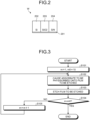
- FIG. 2 is a schematic illustrating one example of a structure of the wafer W.
- the wafer W has a silicon film 202, a silicon oxide film 203, and a silicon nitride film 204 on a substrate 201, as illustrated in FIG. 2 , for example.
- the silicon film 202, the silicon oxide film 203, and the silicon nitride film 204 are arranged adjacently to one another.
- the silicon film 202 and the silicon oxide film 203 are examples of the film to be etched.
- FIG. 3 is a flowchart illustrating one example of the sequence of a process of a plasma etching method according to one embodiment.
- FIG. 4 is a schematic illustrating one example of a cross section of the wafer W after the execution of the steps illustrated in FIG. 3 .
- the plasma etching apparatus 10 execute a series of steps to the wafer W illustrated in FIG. 2 .
- the wafer W that is the object to be processed is carried into the chamber 12c, and is placed on the stage 16.
- the cross section of the wafer W is as illustrated in FIG. 4(a) , for example.
- the plasma etching apparatus 10 sets values to a parameter m for counting the number of times the steps are repeated, and a parameter m0 specifying the upper bound of the number of times the steps are repeated.
- the plasma etching apparatus 10 sets "1" to the parameter m, for example, and sets "10" to the parameter m0, for example (Step S101).
- the value set to the parameter m0 may be any value. If the value set to the parameter m0 is "1", for example, the physisorption step and the etching step are performed once, without repeating the steps.
- the plasma etching apparatus 10 then executes the physisorption step for causing the adsorbate that is based on the first processing gas to be physisorbed onto the film to be etched, while cooling the wafer W to a temperature equal to or lower than the dew point of the first processing gas (Step S102).
- the film to be etched is, for example, the silicon oxide film 203 on the wafer W.
- the first processing gas includes CF gas, for example. CF gas is, for example, C4F8 or C5F8. It is considered that the physisorption between the adsorbate that is based on the first processing gas and the film to be etched takes place due to van der Waals force, for example.
- Van der Waals force is a force by which molecules or atoms are attracted to one another, and the effect of this force becomes greater when the temperature of the molecules or the atoms becomes lower. Therefore, even when the film to be etched does not have any chemical reactivity to the first processing gas, by cooling the wafer W to a temperature equal to or lower than the dew point of the first processing gas, the first processing gas is caused to be physisorbed onto the film to be etched, by van der Waals force.
- the control unit 70 in the plasma etching apparatus 10 cools the wafer W to a temperature equal to or lower than the dew point of C4F8 that is the first processing gas (hereinafter, referred to as "cryogenic temperature", as appropriate) by controlling the temperature of the refrigerant circulating through the flow channel 18f inside the stage 16.
- the control unit 70 then causes the gas source group 40 to supply C4F8 into the chamber 12c as the first processing gas, while keeping the wafer W at the cryogenic temperature.
- the adsorbate that is based on C4F8 is caused to be physisorbed onto the film to be etched, by van der Waals force, in a unit of one atomic layer.
- the cross section of the wafer W after the execution of the physisorption step illustrated as Step S102 is as illustrated in FIG. 4(b) , for example.
- the C4F8-based adsorbate 205 is caused to be physisorbed onto the silicon oxide film 203 that is the film to be etched. Because the entire wafer W is cooled to the cryogenic temperature, the C4F8-based adsorbate 205 is caused to be physisorbed onto the silicon film 202 and the silicon nitride film 204, as well as onto the silicon oxide film 203.
- the plasma etching apparatus 10 then executes the etching step for etching the film to be etched, by causing the adsorbate to react with the film to be etched, using the plasma of the second processing gas (Step S103).
- the second processing gas includes noble gas, for example.
- the noble gas is Ar, for example.
- the control unit 70 in the plasma etching apparatus 10 causes the gas source group 40 to supply Ar into the chamber 12c as the second processing gas, while cooling the wafer W to the cryogenic temperature, so as to replace C4F8 with Ar, and generates Ar plasma by causing the first high-frequency power source 62 to apply the first high-frequency power for generating plasma.
- the control unit 70 may also cause the second high-frequency power source 64 to apply the second high-frequency power for drawing ions.
- the Ar plasma As the Ar plasma is generated, the plasma promotes the collisions of ions (that is, Ar ions) against the adsorbate on the film to be etched, and induces a reaction between the adsorbate and the film to be etched.
- the film to be etched is etched in a unit of one atomic layer, depending on the thickness of the adsorbate.
- the cross section of the wafer W after the etching step illustrated at Step S103, is as illustrated in FIG. 4(c) , for example.
- the silicon oxide film 203 becomes etched selectively, by the thickness corresponding to the thickness of the adsorbate 205.
- the reactions between the adsorbate 205, and the silicon film 202 and the silicon nitride film 204, which are not to be etched, are also induced.
- the silicon film 202 and the silicon nitride film 204 have carbon-containing substances 206, 207, respectively, that are derived from the C4F8-based adsorbate 205, etching of the silicon film 202 and the silicon nitride film 204 is suppressed.
- the plasma etching apparatus 10 determines whether the physisorption step and the etching step have been repeated by the preset number of times, that is, whether the parameter m is equal to or greater than the parameter m0 (Step S104). If the parameter m is less than the parameter m0 (No at Step S104), the plasma etching apparatus 10 increments the parameter m by one (Step S105), shifts the process back to Step S102, and repeats the physisorption step and the etching step. If the parameter m is equal to or greater than the parameter m0 (Yes at Step S104), the plasma etching apparatus 10 ends the process.
- the control unit 70 executes an adjustment step for adjusting the thickness of the adsorbate, by evaporating or subliming a part of the adsorbate having been physisorbed onto the film to be etched, between the physisorption step and the etching step.
- FIG. 5 is a schematic illustrating a time chart of conditions used in the plasma etching method according to one embodiment.
- the control unit 70 in the plasma etching apparatus 10 executes the physisorption step, the adjustment step, and the etching step repeatedly, in the order listed herein, to the wafer W illustrated in FIG. 2 .
- the control unit 70 controls the timing for supplying C4F8, the timing for supplying Ar, the timing for supplying the first high-frequency power, and the timing for supplying the second high-frequency power, in accordance with the time chart illustrated in FIG. 5 .
- the control unit 70 executes the physisorption step for causing the C4F8-based adsorbate 205 to be physisorbed onto the silicon oxide film 203, while cooling the wafer W to a temperature equal to or lower than the dew point of C4F8 (that is, "cryogenic temperature”). Specifically, the control unit 70 supplies C4F8 for a period between time “t0" and time “t1", while keeping the wafer W at the cryogenic temperature, illustrated in FIG. 5 . As a result, the C4F8-based adsorbate 205 is caused to be physisorbed onto the silicon oxide film 203.
- the period between the time "t0" and the time “t1" may be about 2 seconds, for example.
- the control unit 70 then executes the adjustment step for adjusting the thickness of the adsorbate 205 by evaporating or subliming a part of the adsorbate 205 having been physisorbed, as adsorbate, onto the silicon oxide film 203. Specifically, the control unit 70 stops supplying C4F8, and starts supplying Ar at the time "t1", as illustrated in FIG. 5 . As a result, C4F8 is replaced with Ar, and the partial pressure of C4F8 is reduced for a period between the time "t1" and at time "t2".
- the thickness of the C4F8-based adsorbate 205 is adjusted to a predetermined thickness (e.g., the thickness corresponding to one atomic layer).
- the period between the time “t1" and the time “t2" may be about 10 seconds, for example.
- the control unit 70 then executes the etching step for etching the silicon oxide film 203, by causing the adsorbate 205, having been physisorbed as the adsorbate, to react with the silicon oxide film 203, using Ar plasma.
- the control unit 70 generates Ar plasma by applying the first high-frequency power, for a period between the time "t2" and at time "t4", as illustrated in FIG. 5 , while keeping cooling the wafer W and supplying Ar.
- the control unit 70 also draws ions in the plasma into the wafer W by applying the second high-frequency power for a period between time "t3" and the time "t4".
- the plasma promotes collisions of the ions (that is, Ar ions) against the adsorbate 205 on the silicon oxide film 203, and induces the reaction between the C4F8-based adsorbate 205 and the silicon oxide film 203.
- the film to be etched is etched in a unit of one atomic layer, depending on the thickness of the C4F8-based adsorbate 205.
- the period between the time “t2" and the time "t4" may be about 25 seconds, for example, and the period between the time "t3" and the time "t4" may be about 20 seconds, for example.
- the control unit 70 then executes the physisorption step, the adjustment step, and the etching step, a plurality of times, in the order listed herein.
- FIG. 6A is a schematic illustrating a measurement result of the etched amount of the silicon oxide film 203, when a cycle of the physisorption step, the adjustment step, and the etching step was repeated four times, in the order listed herein, with the wafer W cooled to -50°C.
- FIG. 6B is a schematic illustrating a measurement result of the etched amount of the silicon oxide film 203, when the cycle of the physisorption step, the adjustment step, and the etching step was repeated four times, in the order listed herein, with the wafer W cooled to -110°C.
- FIG. 6A is a schematic illustrating a measurement result of the etched amount of the silicon oxide film 203, when a cycle of the physisorption step, the adjustment step, and the etching step was repeated four times, in the order listed herein, with the wafer W cooled to -110°C.
- FIGS. 6A to 6C are schematic illustrating a measurement result of the etched amount of the silicon oxide film 203, when the cycle of the physisorption step, the adjustment step, and the etching step was repeated four times, in the order listed herein, with the wafer W cooled to -120°C.
- "reference” indicates the initial thickness of the silicon oxide film 203
- "ALE 4 cycles” indicates the thickness of the silicon oxide film 203 after the cycle of these steps was repeated four times, in the order listed herein.
- the silicon oxide film 203 was etched by an amount of 0.2 nm. This etched amount did not satisfy a predetermined specification of allowance.
- the silicon oxide film 203 was etched by an amount of 0.1 nm. This etched amount did not satisfy the predetermined specification of allowance.
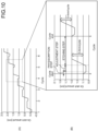
- FIG. 10 is a schematic illustrating a result of measuring the change in the etched amount of the silicon oxide film 203, after the cycle of the physisorption step, the adjustment step, and the etching step was repeated a plurality of times, in the order listed herein, with the wafer W cooled to -120°C.
- FIG. 10(A) illustrates a graph indicating the change in the etched amount of the silicon oxide film 203.
- FIG. 10(B) illustrates an enlargement of the part of the graph corresponding to the fourth cycle in the graph FIG. 10(A) .
- the amount by which the silicon oxide film 203 was etched per one cycle was 0.4 nm.
- the silicon oxide film 203 because the distance between atoms in Si-O bonding is 1.6 to 1.7 angstroms, for example, 0.4 nm corresponds to approximately two atomic layers. In other words, it was confirmed that the silicon oxide film 203 was etched successfully in a unit of one atomic layer, when the temperature of the wafer W was -120°C that is lower than the dew point of C4F8.
- FIG. 7 is a flowchart illustrating another example of the sequence of the process of the plasma etching method according to one embodiment.
- FIG. 8 is a schematic illustrating one example of a cross section of the wafer W after the execution of the steps illustrated in FIG. 7 .
- the plasma etching apparatus 10 executes a series of steps to the wafer W illustrated in FIG. 2 .
- the wafer W that is the object to be processed is carried into the chamber 12c, and placed on the stage 16.
- the cross section of the wafer W is as illustrated in FIG. 8(a) , for example.
- the plasma etching apparatus 10 sets values to the parameter m for counting the number of times the steps are repeated, and the parameter m0 specifying the upper bound of the number of times the steps are repeated.
- the plasma etching apparatus 10 sets "1" to the parameter m, for example, and sets "10" to the parameter m0, for example (Step S111).
- the value set to the parameter m0 may be any value. When the value set to the parameter m0 is "1", for example, the physisorption step and the etching step are performed once, without repeating the steps.
- the plasma etching apparatus 10 then execute a physisorption step for causing a passivation film that is based on the first processing gas to be physisorbed onto the film to be etched, as the adsorbate, while cooling the wafer W to a temperature equal to or lower than the sublimation point of the first processing gas (Step S112).
- the film to be etched is, for example, the silicon film 202 on the wafer W.
- the first processing gas includes, for example, gas including halogen and oxygen. Examples of the gas including halogen and oxygen are SiF4/O2 and S12F6/O2.
- Van der Waals force is a force by which molecules or atoms are attracted to one another, and the effect of this force becomes greater when the temperature of the molecules or the atoms becomes lower. Therefore, even when the film to be etched does not have any chemical reactivity to the first processing gas, by cooling the wafer W to a temperature equal to or lower than the sublimation point of the first processing gas, the passivation film that is based on the first processing gas is caused to be physisorbed onto to the film to be etched, by van der Waals force.
- the control unit 70 in the plasma etching apparatus 10 cools the wafer W to a temperature equal to or lower than the sublimation point of SiF4/O2 that is the first processing gas (hereinafter, referred to as "cryogenic temperature", as appropriate), by controlling the temperature of the refrigerant circulating through the flow channel 18f inside the stage 16.
- the control unit 70 then causes the gas source group 40 to supply SiF4/O2 into the chamber 12c as the first processing gas, while keeping the wafer W at the cryogenic temperature, and generates SiF4/O2 plasma by causing the first high-frequency power source 62 to apply the first high-frequency power for plasma generation.
- control unit 70 may also cause the second high-frequency power source 64 to apply the second high-frequency power for drawing ions.
- an oxide film that is the passivation film based on SiF4/O2 is caused to be physisorbed onto the film to be etched, by van der Waals force, in a unit of one atomic layer.
- the cross section of the wafer W after the execution of the physisorption step illustrated as Step S112 is as illustrated in FIG. 8(b) , for example.
- the SiF4/O2 plasma being generated while the wafer W is cooled to the cryogenic temperature, the physisorption of an oxide film 215 that is SiF4/O2-based passivation film is caused to be physisorbed onto the silicon film 202 that is the film to be etched. Because the entire wafer W is cooled to the cryogenic temperature, the oxide film 215 that is based on SiF4/O2 is caused to be physisorbed not only onto the silicon film 202 but also onto the silicon oxide film 203 and the silicon nitride film 204.
- the plasma etching apparatus 10 then executes the etching step for etching the film to be etched, by causing the adsorbate to react with the film to be etched, using the plasma of the second processing gas (Step S113).
- the second processing gas includes noble gas, for example.
- the noble gas is Ar, for example.
- the control unit 70 in the plasma etching apparatus 10 causes the gas source group 40 to supply Ar into the chamber 12c, as the second processing gas, so as to replace SiF4/O2 with Ar, and generates Ar plasma by causing the first high-frequency power source 62 to apply the first high-frequency power for generating plasma.
- the control unit 70 may also cause the second high-frequency power source 64 to apply the second high-frequency power for drawing ions.
- this plasma promotes the collisions of ions (that is, Ar ions) against the adsorbate on the film to be etched, and induces a reaction between the adsorbate and the film to be etched.
- the film to be etched is etched in a unit of one atomic layer, depending on the thickness of the adsorbate.
- the cross section of the wafer W after the etching step illustrated at Step S113 is as illustrated in FIG. 8(c) , for example.
- the silicon film 202 becomes etched selectively, by the thickness corresponding to the thickness of the oxide film 215.
- the silicon oxide film 203 and the silicon nitride film 204 which are not to be etched, have higher bond-dissociation energy than that of the silicon film 202, therefore, reactions of the silicon oxide film 203 and the silicon nitride film 204, with the oxide film 215 are suppressed. For this reason, etching of the silicon oxide film 203 and the silicon nitride film 204 is suppressed.
- the plasma etching apparatus 10 determines whether the physisorption step and the etching step have been repeated by the preset number of times, that is, whether the parameter m is equal to or greater than the parameter m0 (Step S114). If the parameter m is less than the parameter m0 (No at Step S114), the plasma etching apparatus 10 increments the parameter m by one (Step S115), shifts the process back to Step S112, and repeats the physisorption step and the etching step. If the parameter m is equal to or greater than the parameter m0 (Yes at Step S114), the plasma etching apparatus 10 ends the process.
- the control unit 70 executes an adjustment step for adjusting the thickness of the adsorbate, by evaporating or subliming a part of the adsorbate having been physisorbed onto the film to be etched, between the physisorption step and the etching step.
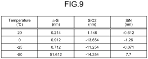
- FIG. 9 is a schematic illustrating one example of a relation between the temperature of the wafer W cooled at the physisorption step, and the etched amounts of the silicon film 202, the silicon oxide film 203, and the silicon nitride film 204.
- temperature (°C) represents the temperature (°C) of the wafer W cooled at the physisorption step.
- a-Si (nm) represents the amount (nm) by which the silicon film 202 was etched
- SiO2 (nm) represents the amount (nm) by which the silicon oxide film 203 was etched
- SiN (nm) represents the amount (nm) by which the silicon nitride film 204 was etched.
- the etch amount of the silicon film 202 increased to 51.612 (nm).
- the etch amounts of the silicon oxide film 203 and the silicon nitride film 204 were smaller than that of the silicon film 202. This can be attributed to the fact that the silicon oxide film 203 and the silicon nitride film 204 have higher bond-dissociation energy than that of the silicon film 202.
- an adsorbate that is based on the first processing gas is caused to be physisorbed onto a film to be etched, while cooling object to be processed on which the film to be etched is provided, and the film to be etched is etched by causing the adsorbate to react with the film to be etched, using plasma of the second processing gas. Therefore, it is possible to remove the limitation imposed on the selectable film to be etched with respect to to the substance having chemical reactivity to the first processing gas, and to control the etch amount of the film to be etched easily, in a unit of one atomic layer, based on the thickness of the adsorbate. As a result, an implementation of self-limiting etching, with no limitation on the film to be etched is made possible.
Landscapes
- Drying Of Semiconductors (AREA)
- Physics & Mathematics (AREA)
- Engineering & Computer Science (AREA)
- Plasma & Fusion (AREA)
- Manufacturing Of Printed Circuit Boards (AREA)
- Semiconductor Memories (AREA)
Claims (6)
- Plasmaätzverfahren, umfassend:einen Physisorptionsschritt (S102, S112) zum Bewirken, dass ein Adsorbat (205, 215), das auf einem ersten Prozessgas basiert, auf einem zu ätzenden Film physisorbiert wird, während ein zu bearbeitendes Objekt (W) gekühlt wird, auf dem der zu ätzende Film vorgesehen ist, wobei der zu ätzende Film keinerlei chemische Reaktivität gegenüber dem ersten Prozessgas aufweist;einen Anpassungsschritt zum Anpassen einer Dicke des Adsorbats (205, 215) durch Verdampfen oder Sublimieren eines Teils des Adsorbats (205, 215), der auf dem zu ätzenden Film physisorbiert wurde; undeinen Ätzschritt (S103, S113) zum Ätzen des zu ätzenden Films, indem bewirkt wird, dass das Adsorbat (205, 215) unter Verwendung eines Plasmas eines zweiten Prozessgases mit dem zu ätzenden Film reagiert.
- Plasmaätzverfahren nach Anspruch 1, wobei der Physisorptionsschritt (S102, S112) und der Ätzschritt (S103, S113) abwechselnd eine Vielzahl von Malen wiederholt werden.
- Plasmaätzverfahren nach Anspruch 1 oder Anspruch 2, wobeider zu ätzende Film ein Siliziumoxidfilm (203) ist, unddas erste Prozessgas CF-Gas einschließt.
- Plasmaätzverfahren nach Anspruch 1 oder Anspruch 2, wobeider zu ätzende Film ein Siliziumfilm (202) ist, unddas erste Prozessgas Gas einschließt, das ein Halogen und Sauerstoff einschließt.
- Plasmaätzverfahren nach Anspruch 1, wobei das zweite Prozessgas ein Edelgas einschließt.
- Plasmaätzvorrichtung (10), umfassend:eine Kammer (12), in der ein Plasmaätzverfahren an einem zu bearbeitenden Objekt (W) durchgeführt wird;eine Ablufteinheit (50), die dazu angeordnet ist, Druck in der Kammer (12) zu verringern;eine Gaszufuhreinheit, die dazu angeordnet ist, ein Prozessgas in die Kammer (12) zuzuführen; undeine Steuereinheit (70), die dazu angeordnet ist, einen Physisorptionsschritt (S102, S112) auszuführen, um zu bewirken, dass ein auf einem ersten Prozessgas basierendes Adsorbat (205, 215) auf einem zu ätzenden Film physisorbiert wird, während ein zu bearbeitendes Objekt (W) gekühlt wird, auf dem der zu ätzende Film vorgesehen ist, wobei der zu ätzende Film keinerlei chemische Reaktivität gegenüber dem ersten Prozessgas aufweist, und angeordnet ist zum Ausführen eines Anpassungsschritts zum Anpassen einer Dicke des Adsorbats (205, 215) durch Verdampfen oder Sublimieren eines Teils des Adsorbats (205, 215), der auf dem zu ätzenden Film physisorbiert wurde; und eines Ätzschritts (S103, S113) zum Ätzen des zu ätzenden Films, indem bewirkt wird, dass das Adsorbat (205, 215) unter Verwendung eines Plasmas eines zweiten Prozessgases mit dem zu ätzenden Film reagiert.
Applications Claiming Priority (2)
| Application Number | Priority Date | Filing Date | Title |
|---|---|---|---|
| JP2017240333 | 2017-12-15 | ||
| PCT/JP2018/045461 WO2019117130A1 (ja) | 2017-12-15 | 2018-12-11 | プラズマエッチング方法及びプラズマエッチング装置 |
Publications (4)
| Publication Number | Publication Date |
|---|---|
| EP3726567A1 EP3726567A1 (de) | 2020-10-21 |
| EP3726567A4 EP3726567A4 (de) | 2021-08-25 |
| EP3726567B1 true EP3726567B1 (de) | 2025-01-22 |
| EP3726567C0 EP3726567C0 (de) | 2025-01-22 |
Family
ID=66820859
Family Applications (1)
| Application Number | Title | Priority Date | Filing Date |
|---|---|---|---|
| EP18889001.6A Active EP3726567B1 (de) | 2017-12-15 | 2018-12-11 | Plasmaätzverfahren und plasmaätzvorrichtung |
Country Status (8)
| Country | Link |
|---|---|
| US (1) | US11120999B2 (de) |
| EP (1) | EP3726567B1 (de) |
| JP (1) | JP6976352B2 (de) |
| KR (1) | KR102790129B1 (de) |
| CN (1) | CN111527591B (de) |
| SG (1) | SG11202004968SA (de) |
| TW (1) | TWI809020B (de) |
| WO (1) | WO2019117130A1 (de) |
Families Citing this family (5)
| Publication number | Priority date | Publication date | Assignee | Title |
|---|---|---|---|---|
| JP7413093B2 (ja) * | 2019-07-18 | 2024-01-15 | キオクシア株式会社 | エッチング方法、半導体製造装置、および半導体装置の製造方法 |
| JP7437966B2 (ja) * | 2020-02-21 | 2024-02-26 | 東京エレクトロン株式会社 | エッチング方法及びエッチング装置 |
| KR102792064B1 (ko) | 2022-10-05 | 2025-04-04 | 충남대학교산학협력단 | 가스 펄싱을 이용한 원자층 식각 방법 |
| US20250201569A1 (en) * | 2023-12-14 | 2025-06-19 | Applied Materials, Inc. | Etching substrates using vapor adsorption |
| JP2026048218A (ja) * | 2024-09-05 | 2026-03-17 | 東京エレクトロン株式会社 | 基板処理方法、及び基板処理装置 |
Citations (1)
| Publication number | Priority date | Publication date | Assignee | Title |
|---|---|---|---|---|
| EP2911187A1 (de) * | 2014-02-24 | 2015-08-26 | Tokyo Electron Limited | Ätzverfahren |
Family Cites Families (12)
| Publication number | Priority date | Publication date | Assignee | Title |
|---|---|---|---|---|
| JPH03138369A (ja) | 1989-10-24 | 1991-06-12 | Sony Corp | 低温処理装置 |
| JPH03263827A (ja) | 1990-03-14 | 1991-11-25 | Yasuhiro Horiike | デジタルエツチング装置 |
| JPH03276719A (ja) * | 1990-03-27 | 1991-12-06 | Yasuhiro Horiike | デジタルエツチング方法 |
| JPH05217949A (ja) * | 1992-02-07 | 1993-08-27 | Oki Electric Ind Co Ltd | ドライエッチング装置及びその方法 |
| JPH07106305A (ja) | 1993-10-06 | 1995-04-21 | Hitachi Ltd | 原子層エッチング装置 |
| JP3660910B2 (ja) | 2002-03-06 | 2005-06-15 | 日本ビクター株式会社 | 情報記録媒体、情報記録媒体のセクタ読取り方法、情報記録媒体のセクタ読取りプログラム、情報記録媒体のセクタ読取り方法及び真贋判定方法、情報記録媒体のセクタ読取りプログラム及び真贋判定プログラム |
| JP6032033B2 (ja) * | 2013-02-01 | 2016-11-24 | セントラル硝子株式会社 | シリコンのドライエッチング方法 |
| US9609730B2 (en) | 2014-11-12 | 2017-03-28 | Lam Research Corporation | Adjustment of VUV emission of a plasma via collisional resonant energy transfer to an energy absorber gas |
| JP6818402B2 (ja) | 2015-07-17 | 2021-01-20 | 株式会社日立ハイテク | プラズマ処理装置 |
| JP6212092B2 (ja) * | 2015-10-02 | 2017-10-11 | 東京エレクトロン株式会社 | 基板処理システム、フォーカスリングの温度制御方法及び基板のエッチング方法 |
| US10566212B2 (en) * | 2016-12-19 | 2020-02-18 | Lam Research Corporation | Designer atomic layer etching |
| US10134600B2 (en) * | 2017-02-06 | 2018-11-20 | Lam Research Corporation | Dielectric contact etch |
-
2018
- 2018-12-11 CN CN201880078824.7A patent/CN111527591B/zh active Active
- 2018-12-11 SG SG11202004968SA patent/SG11202004968SA/en unknown
- 2018-12-11 WO PCT/JP2018/045461 patent/WO2019117130A1/ja not_active Ceased
- 2018-12-11 EP EP18889001.6A patent/EP3726567B1/de active Active
- 2018-12-11 US US16/770,084 patent/US11120999B2/en active Active
- 2018-12-11 JP JP2019559649A patent/JP6976352B2/ja active Active
- 2018-12-11 KR KR1020207016218A patent/KR102790129B1/ko active Active
- 2018-12-14 TW TW107145219A patent/TWI809020B/zh active
Patent Citations (1)
| Publication number | Priority date | Publication date | Assignee | Title |
|---|---|---|---|---|
| EP2911187A1 (de) * | 2014-02-24 | 2015-08-26 | Tokyo Electron Limited | Ätzverfahren |
Also Published As
| Publication number | Publication date |
|---|---|
| US11120999B2 (en) | 2021-09-14 |
| KR102790129B1 (ko) | 2025-04-01 |
| KR20200094751A (ko) | 2020-08-07 |
| EP3726567A4 (de) | 2021-08-25 |
| JP6976352B2 (ja) | 2021-12-08 |
| TW201931465A (zh) | 2019-08-01 |
| WO2019117130A1 (ja) | 2019-06-20 |
| EP3726567A1 (de) | 2020-10-21 |
| US20200381264A1 (en) | 2020-12-03 |
| SG11202004968SA (en) | 2020-07-29 |
| CN111527591A (zh) | 2020-08-11 |
| CN111527591B (zh) | 2024-08-13 |
| JPWO2019117130A1 (ja) | 2021-02-18 |
| EP3726567C0 (de) | 2025-01-22 |
| TWI809020B (zh) | 2023-07-21 |
Similar Documents
| Publication | Publication Date | Title |
|---|---|---|
| EP3726567B1 (de) | Plasmaätzverfahren und plasmaätzvorrichtung | |
| US9859126B2 (en) | Method for processing target object | |
| US9685305B2 (en) | Plasma processing apparatus and plasma processing method | |
| TWI686863B (zh) | 蝕刻有機膜之方法 | |
| JP6366454B2 (ja) | 被処理体を処理する方法 | |
| US9607811B2 (en) | Workpiece processing method | |
| JP6298391B2 (ja) | プラズマ処理方法及びプラズマ処理装置 | |
| JP5956933B2 (ja) | プラズマ処理方法及びプラズマ処理装置 | |
| KR20170009843A (ko) | 플라즈마 처리 방법 및 플라즈마 처리 장치 | |
| JP2017010993A (ja) | プラズマ処理方法 | |
| KR20180018416A (ko) | 피처리체를 처리하는 방법 | |
| US10233535B2 (en) | Plasma processing apparatus and plasma processing method | |
| US8328981B2 (en) | Method for heating a focus ring in a plasma apparatus by high frequency power while no plasma being generated | |
| US11610766B2 (en) | Target object processing method and plasma processing apparatus | |
| KR102735318B1 (ko) | 클리닝 방법 및 플라즈마 처리 장치 | |
| JP7160291B2 (ja) | エッチング方法、及びエッチング装置 |
Legal Events
| Date | Code | Title | Description |
|---|---|---|---|
| STAA | Information on the status of an ep patent application or granted ep patent |
Free format text: STATUS: THE INTERNATIONAL PUBLICATION HAS BEEN MADE |
|
| PUAI | Public reference made under article 153(3) epc to a published international application that has entered the european phase |
Free format text: ORIGINAL CODE: 0009012 |
|
| STAA | Information on the status of an ep patent application or granted ep patent |
Free format text: STATUS: REQUEST FOR EXAMINATION WAS MADE |
|
| 17P | Request for examination filed |
Effective date: 20200528 |
|
| AK | Designated contracting states |
Kind code of ref document: A1 Designated state(s): AL AT BE BG CH CY CZ DE DK EE ES FI FR GB GR HR HU IE IS IT LI LT LU LV MC MK MT NL NO PL PT RO RS SE SI SK SM TR |
|
| AX | Request for extension of the european patent |
Extension state: BA ME |
|
| DAV | Request for validation of the european patent (deleted) | ||
| DAX | Request for extension of the european patent (deleted) | ||
| A4 | Supplementary search report drawn up and despatched |
Effective date: 20210727 |
|
| RIC1 | Information provided on ipc code assigned before grant |
Ipc: H01L 21/3065 20060101AFI20210721BHEP Ipc: H01L 21/311 20060101ALI20210721BHEP |
|
| STAA | Information on the status of an ep patent application or granted ep patent |
Free format text: STATUS: EXAMINATION IS IN PROGRESS |
|
| 17Q | First examination report despatched |
Effective date: 20231109 |
|
| GRAP | Despatch of communication of intention to grant a patent |
Free format text: ORIGINAL CODE: EPIDOSNIGR1 |
|
| STAA | Information on the status of an ep patent application or granted ep patent |
Free format text: STATUS: GRANT OF PATENT IS INTENDED |
|
| RIC1 | Information provided on ipc code assigned before grant |
Ipc: H01L 21/311 20060101ALI20240731BHEP Ipc: H01L 21/3065 20060101AFI20240731BHEP |
|
| RIN1 | Information on inventor provided before grant (corrected) |
Inventor name: ANTOUN, GAELLE Inventor name: LEFAUCHEUX, PHILIPPE Inventor name: TILLOCHER, THOMAS Inventor name: DUSSART, REMI Inventor name: FAGUET, JACQUES Inventor name: TAHARA, SHIGERU Inventor name: ONO, KUMIKO Inventor name: SATO, NAGISA Inventor name: MAEKAWA, KAORU Inventor name: YATSUDA, KOICHI |
|
| INTG | Intention to grant announced |
Effective date: 20240829 |
|
| RAP3 | Party data changed (applicant data changed or rights of an application transferred) |
Owner name: UNIVERSITE D'ORLEANS Owner name: TOKYO ELECTRON LIMITED |
|
| GRAS | Grant fee paid |
Free format text: ORIGINAL CODE: EPIDOSNIGR3 |
|
| GRAA | (expected) grant |
Free format text: ORIGINAL CODE: 0009210 |
|
| STAA | Information on the status of an ep patent application or granted ep patent |
Free format text: STATUS: THE PATENT HAS BEEN GRANTED |
|
| AK | Designated contracting states |
Kind code of ref document: B1 Designated state(s): AL AT BE BG CH CY CZ DE DK EE ES FI FR GB GR HR HU IE IS IT LI LT LU LV MC MK MT NL NO PL PT RO RS SE SI SK SM TR |
|
| REG | Reference to a national code |
Ref country code: GB Ref legal event code: FG4D |
|
| REG | Reference to a national code |
Ref country code: CH Ref legal event code: EP |
|
| REG | Reference to a national code |
Ref country code: IE Ref legal event code: FG4D |
|
| REG | Reference to a national code |
Ref country code: DE Ref legal event code: R096 Ref document number: 602018078756 Country of ref document: DE |
|
| U01 | Request for unitary effect filed |
Effective date: 20250122 |
|
| U07 | Unitary effect registered |
Designated state(s): AT BE BG DE DK EE FI FR IT LT LU LV MT NL PT RO SE SI Effective date: 20250128 |
|
| PG25 | Lapsed in a contracting state [announced via postgrant information from national office to epo] |
Ref country code: RS Free format text: LAPSE BECAUSE OF FAILURE TO SUBMIT A TRANSLATION OF THE DESCRIPTION OR TO PAY THE FEE WITHIN THE PRESCRIBED TIME-LIMIT Effective date: 20250422 |
|
| PG25 | Lapsed in a contracting state [announced via postgrant information from national office to epo] |
Ref country code: PL Free format text: LAPSE BECAUSE OF FAILURE TO SUBMIT A TRANSLATION OF THE DESCRIPTION OR TO PAY THE FEE WITHIN THE PRESCRIBED TIME-LIMIT Effective date: 20250122 |
|
| PG25 | Lapsed in a contracting state [announced via postgrant information from national office to epo] |
Ref country code: ES Free format text: LAPSE BECAUSE OF FAILURE TO SUBMIT A TRANSLATION OF THE DESCRIPTION OR TO PAY THE FEE WITHIN THE PRESCRIBED TIME-LIMIT Effective date: 20250122 |
|
| PG25 | Lapsed in a contracting state [announced via postgrant information from national office to epo] |
Ref country code: IS Free format text: LAPSE BECAUSE OF FAILURE TO SUBMIT A TRANSLATION OF THE DESCRIPTION OR TO PAY THE FEE WITHIN THE PRESCRIBED TIME-LIMIT Effective date: 20250522 Ref country code: NO Free format text: LAPSE BECAUSE OF FAILURE TO SUBMIT A TRANSLATION OF THE DESCRIPTION OR TO PAY THE FEE WITHIN THE PRESCRIBED TIME-LIMIT Effective date: 20250422 |
|
| PG25 | Lapsed in a contracting state [announced via postgrant information from national office to epo] |
Ref country code: HR Free format text: LAPSE BECAUSE OF FAILURE TO SUBMIT A TRANSLATION OF THE DESCRIPTION OR TO PAY THE FEE WITHIN THE PRESCRIBED TIME-LIMIT Effective date: 20250122 |
|
| PG25 | Lapsed in a contracting state [announced via postgrant information from national office to epo] |
Ref country code: GR Free format text: LAPSE BECAUSE OF FAILURE TO SUBMIT A TRANSLATION OF THE DESCRIPTION OR TO PAY THE FEE WITHIN THE PRESCRIBED TIME-LIMIT Effective date: 20250423 |
|
| PG25 | Lapsed in a contracting state [announced via postgrant information from national office to epo] |
Ref country code: SM Free format text: LAPSE BECAUSE OF FAILURE TO SUBMIT A TRANSLATION OF THE DESCRIPTION OR TO PAY THE FEE WITHIN THE PRESCRIBED TIME-LIMIT Effective date: 20250122 |
|
| PG25 | Lapsed in a contracting state [announced via postgrant information from national office to epo] |
Ref country code: CZ Free format text: LAPSE BECAUSE OF FAILURE TO SUBMIT A TRANSLATION OF THE DESCRIPTION OR TO PAY THE FEE WITHIN THE PRESCRIBED TIME-LIMIT Effective date: 20250122 |
|
| PG25 | Lapsed in a contracting state [announced via postgrant information from national office to epo] |
Ref country code: SK Free format text: LAPSE BECAUSE OF FAILURE TO SUBMIT A TRANSLATION OF THE DESCRIPTION OR TO PAY THE FEE WITHIN THE PRESCRIBED TIME-LIMIT Effective date: 20250122 |
|
| PLBE | No opposition filed within time limit |
Free format text: ORIGINAL CODE: 0009261 |
|
| STAA | Information on the status of an ep patent application or granted ep patent |
Free format text: STATUS: NO OPPOSITION FILED WITHIN TIME LIMIT |
|
| 26N | No opposition filed |
Effective date: 20251023 |
|
| U20 | Renewal fee for the european patent with unitary effect paid |
Year of fee payment: 8 Effective date: 20251229 |