EP3721294B1 - Systems and methods for device-correlated overlay metrology - Google Patents
Systems and methods for device-correlated overlay metrology Download PDFInfo
- Publication number
- EP3721294B1 EP3721294B1 EP18886399.7A EP18886399A EP3721294B1 EP 3721294 B1 EP3721294 B1 EP 3721294B1 EP 18886399 A EP18886399 A EP 18886399A EP 3721294 B1 EP3721294 B1 EP 3721294B1
- Authority
- EP
- European Patent Office
- Prior art keywords
- layer
- overlay
- pattern
- features
- additional
- Prior art date
- Legal status (The legal status is an assumption and is not a legal conclusion. Google has not performed a legal analysis and makes no representation as to the accuracy of the status listed.)
- Active
Links
Images


Classifications
-
- G—PHYSICS
- G03—PHOTOGRAPHY; CINEMATOGRAPHY; ANALOGOUS TECHNIQUES USING WAVES OTHER THAN OPTICAL WAVES; ELECTROGRAPHY; HOLOGRAPHY
- G03F—PHOTOMECHANICAL PRODUCTION OF TEXTURED OR PATTERNED SURFACES, e.g. FOR PRINTING, FOR PROCESSING OF SEMICONDUCTOR DEVICES; MATERIALS THEREFOR; ORIGINALS THEREFOR; APPARATUS SPECIALLY ADAPTED THEREFOR
- G03F7/00—Photomechanical, e.g. photolithographic, production of textured or patterned surfaces, e.g. printing surfaces; Materials therefor, e.g. comprising photoresists; Apparatus specially adapted therefor
- G03F7/70—Microphotolithographic exposure; Apparatus therefor
- G03F7/70483—Information management; Active and passive control; Testing; Wafer monitoring, e.g. pattern monitoring
- G03F7/70605—Workpiece metrology
- G03F7/70616—Monitoring the printed patterns
- G03F7/70633—Overlay, i.e. relative alignment between patterns printed by separate exposures in different layers, or in the same layer in multiple exposures or stitching
-
- G—PHYSICS
- G01—MEASURING; TESTING
- G01B—MEASURING LENGTH, THICKNESS OR SIMILAR LINEAR DIMENSIONS; MEASURING ANGLES; MEASURING AREAS; MEASURING IRREGULARITIES OF SURFACES OR CONTOURS
- G01B11/00—Measuring arrangements characterised by the use of optical techniques
- G01B11/26—Measuring arrangements characterised by the use of optical techniques for measuring angles or tapers; for testing the alignment of axes
- G01B11/27—Measuring arrangements characterised by the use of optical techniques for measuring angles or tapers; for testing the alignment of axes for testing the alignment of axes
- G01B11/272—Measuring arrangements characterised by the use of optical techniques for measuring angles or tapers; for testing the alignment of axes for testing the alignment of axes using photoelectric detection means
-
- G—PHYSICS
- G03—PHOTOGRAPHY; CINEMATOGRAPHY; ANALOGOUS TECHNIQUES USING WAVES OTHER THAN OPTICAL WAVES; ELECTROGRAPHY; HOLOGRAPHY
- G03F—PHOTOMECHANICAL PRODUCTION OF TEXTURED OR PATTERNED SURFACES, e.g. FOR PRINTING, FOR PROCESSING OF SEMICONDUCTOR DEVICES; MATERIALS THEREFOR; ORIGINALS THEREFOR; APPARATUS SPECIALLY ADAPTED THEREFOR
- G03F7/00—Photomechanical, e.g. photolithographic, production of textured or patterned surfaces, e.g. printing surfaces; Materials therefor, e.g. comprising photoresists; Apparatus specially adapted therefor
- G03F7/70—Microphotolithographic exposure; Apparatus therefor
- G03F7/70483—Information management; Active and passive control; Testing; Wafer monitoring, e.g. pattern monitoring
- G03F7/70605—Workpiece metrology
- G03F7/70616—Monitoring the printed patterns
-
- G—PHYSICS
- G03—PHOTOGRAPHY; CINEMATOGRAPHY; ANALOGOUS TECHNIQUES USING WAVES OTHER THAN OPTICAL WAVES; ELECTROGRAPHY; HOLOGRAPHY
- G03F—PHOTOMECHANICAL PRODUCTION OF TEXTURED OR PATTERNED SURFACES, e.g. FOR PRINTING, FOR PROCESSING OF SEMICONDUCTOR DEVICES; MATERIALS THEREFOR; ORIGINALS THEREFOR; APPARATUS SPECIALLY ADAPTED THEREFOR
- G03F7/00—Photomechanical, e.g. photolithographic, production of textured or patterned surfaces, e.g. printing surfaces; Materials therefor, e.g. comprising photoresists; Apparatus specially adapted therefor
- G03F7/70—Microphotolithographic exposure; Apparatus therefor
- G03F7/70483—Information management; Active and passive control; Testing; Wafer monitoring, e.g. pattern monitoring
- G03F7/70605—Workpiece metrology
- G03F7/706835—Metrology information management or control
-
- H—ELECTRICITY
- H01—ELECTRIC ELEMENTS
- H01L—SEMICONDUCTOR DEVICES NOT COVERED BY CLASS H10
- H01L22/00—Testing or measuring during manufacture or treatment; Reliability measurements, i.e. testing of parts without further processing to modify the parts as such; Structural arrangements therefor
- H01L22/20—Sequence of activities consisting of a plurality of measurements, corrections, marking or sorting steps
-
- G—PHYSICS
- G01—MEASURING; TESTING
- G01B—MEASURING LENGTH, THICKNESS OR SIMILAR LINEAR DIMENSIONS; MEASURING ANGLES; MEASURING AREAS; MEASURING IRREGULARITIES OF SURFACES OR CONTOURS
- G01B15/00—Measuring arrangements characterised by the use of electromagnetic waves or particle radiation, e.g. by the use of microwaves, X-rays, gamma rays or electrons
-
- G—PHYSICS
- G01—MEASURING; TESTING
- G01B—MEASURING LENGTH, THICKNESS OR SIMILAR LINEAR DIMENSIONS; MEASURING ANGLES; MEASURING AREAS; MEASURING IRREGULARITIES OF SURFACES OR CONTOURS
- G01B2210/00—Aspects not specifically covered by any group under G01B, e.g. of wheel alignment, caliper-like sensors
- G01B2210/56—Measuring geometric parameters of semiconductor structures, e.g. profile, critical dimensions or trench depth
-
- H—ELECTRICITY
- H01—ELECTRIC ELEMENTS
- H01L—SEMICONDUCTOR DEVICES NOT COVERED BY CLASS H10
- H01L22/00—Testing or measuring during manufacture or treatment; Reliability measurements, i.e. testing of parts without further processing to modify the parts as such; Structural arrangements therefor
- H01L22/10—Measuring as part of the manufacturing process
- H01L22/12—Measuring as part of the manufacturing process for structural parameters, e.g. thickness, line width, refractive index, temperature, warp, bond strength, defects, optical inspection, electrical measurement of structural dimensions, metallurgic measurement of diffusions
Definitions
- the present disclosure relates generally to overlay metrology and, more particularly, to overlay metrology targets for device-correlated overlay metrology.
- Overlay metrology is the measurement of the relative positions of structures on various layers of a sample, which are critical to the performance of a fabricated device and must typically be controlled within tight tolerances. For example, overlay metrology may measure the relative positions of features on different sample layers as a measure of the layer-by-layer alignment of fabrication tools.
- overlay measurements may damage or otherwise affect the performance of device features. Accordingly, overlay measurements are commonly performed on dedicated overlay targets having features designed for sensitive overlay measurements rather than directly on device features. However, differences in size, orientation, density, and/or location on the sample of overlay targets relative to the device features may introduce a mismatch between measured overlay at the target and actual overlay of device features. For example, features on different layers of overlay targets are commonly spatially separated to avoid overlap and facilitate measurements of features on buried layers. However, open areas associated with spatially separated features may not be compatible with microelectronics fabrication. Further, device features commonly include stacked structures such that overlay measurements of spatially separated features may introduce measurement errors.
- EP3171396 discloses a method of determining an overlay error during manufacturing of a multilayer semiconductor device.
- KUIPER STEFAN ET AL "Large Dynamic Range Atomic Force Microscope for Overlay Improvements", PROCEEDINGS OF SPIE, vol. 9778, 8 March 2016 .
- WO2004090980 discloses an overlay metrology mark.
- An overlay metrology system as recited in claim 1 is disclosed.
- Embodiments of the present disclosure are directed to systems and methods for measuring device-correlated overlay using overlay targets with stacked device-scale features based on a combination of intra-layer and inter-layer measurements.
- an overlay target may include stacked device-scale features on multiple layers such that a device-relevant overlay measurement may be based on the relative positions of the device-scale features.
- direct measurement of the relative positions of stacked device-scale features may be impractical or undesirable.
- a semiconductor device may by formed as multiple printed layers of patterned material on a substrate.
- Each printed layer may be fabricated through a series of process steps such as, but not limited to, one or more material deposition steps, one or more lithography steps, or one or more etching steps.
- each printed layer must be fabricated within specific tolerances to properly construct the final device. For example, printing characteristics such as, but not limited to, the linewidths, sidewall angles, and relative placement of printed elements in each layer must be well characterized and controlled.
- metrology targets may be fabricated on one or more printed layers to enable efficient characterization of the fabrication process.
- deviations of printed characteristics of metrology targets on a printed layer may be representative of deviations of printed characteristics of all printed elements on the layer including device features forming a portion of the semiconductor device.
- optical metrology tools e.g., light-based metrology tools using electromagnetic radiation for illumination and/or detection
- PPE pattern placement errors
- scatterometry in which overlay is determined based on light scattered and/or diffracted from diffraction gratings on multiple layers.
- optical metrology tools For the purposes of the present disclosure, the term “optical metrology tools,” “optical metrology techniques,” and the like indicate metrology tools and techniques using electromagnetic radiation of any wavelength such as, but not limited to, x-ray wavelengths, extreme ultraviolet (EUV) wavelengths, vacuum ultraviolet (VUV) wavelengths, deep ultraviolet (DUV) wavelengths, ultraviolet (UV) wavelengths, visible wavelengths, or infrared (IR) wavelengths.
- EUV extreme ultraviolet
- VUV vacuum ultraviolet
- DUV deep ultraviolet
- UV ultraviolet
- IR infrared
- particle-based metrology tools such as, but not limited to, a scanning electron microscope (SEM) metrology tool (e.g., a critical dimension SEM (CD-SEM), or the like), or a focused ion beam (FIB) metrology tool may resolve device-scale features.
- SEM scanning electron microscope
- FIB focused ion beam
- particle-beam metrology tools may have a limited ability to simultaneously measure features on multiple sample layers based on the particle penetration depth. For example, low-energy particle beams may be used to characterize a top layer (e.g., a current layer), while relatively higher-energy particle beams may penetrate deeper into the sample to characterize features on previously-fabricated layers.
- Embodiments of the present disclosure are directed to systems and methods for measuring device-correlated overlay using intra-layer measurements of device-scale features and reference features coupled with inter-layer overlay measurements of the reference features.
- Layers of an overlay target may thus include device-scale features suitable for intra-layer measurements as well as reference features suitable for both intra-layer and inter-layer measurements.
- embodiments of the present disclosure are directed to overlay targets suitable for measuring overlay of any number of sample layers (e.g., two or more sample layers).
- PPE pattern placement error
- a device-correlated overlay measurement between a first layer and a second layer may be determined based on a measurement of a distance D 1 between a selected device-scale feature and a selected reference features on the first layer after the fabrication of the first layer, a measurement of a distance D 2 between a selected device-scale feature and a selected reference features on the second layer after the fabrication of the second layer, and a through-target overlay measurement OVL ref of reference features on the first and second layers.
- the reference features may have any dimensions and may be designed for any type of overlay measurement known in the art such as, but not limited to, optical overlay measurements, particle-based overlay measurements, or PPE measurements.
- the reference features may have different dimensions than the device-scale features to facilitate inter-layer overlay measurements.
- reference features suitable for optical measurement may have dimensions selected to be greater than the optical resolution of a selected optical metrology tool.
- reference features suitable for particle-based measurement may have dimensions selected to be greater than a resolution of a selected particle-based metrology tool at each layer. It is recognized herein that the resolution of a particle-based metrology system may be higher for surface-level features than for sub-surface features located on sub-surface layers due to particle-sample interactions such as, but not limited to particle scattering in the material. Accordingly, it may be the case that a particle-based metrology system may accurately resolve device-scale features on a surface layer, but may not accurately resolve (e.g., within selected tolerances) device-scale features on a sub-surface layer, particularly if the sub-surface features are stacked below the surface-level features. In this regard, the dimensions of the reference features on any layer may be selected to be resolvable by the metrology system within identified tolerances.
- the pattern placement error PPE may be influenced by multiple factors. For example, as described previously herein, the placement of features within an exposure field of a lithography tool may be influenced by the size, shape, density, and/or orientation of the features. Accordingly, any differences between the reference features and the device-scale features on a given layer may result in pattern placement errors.
- intra-field fabrication errors may be induced by aberrations in a lithography tool during an exposure step such as, but not limited to, lens aberrations or turbulence caused by heat in the lithography tool.
- equation (2) above expressing overlay between two sample layers and the associated description is provided only for illustrative purposes and should not be interpreted as limiting.
- device-correlated overlays may be generated for any number of sample layers.
- the device correlated overlays of equations (1) and/or (2) may represent overlay between any two layers of a multi-layer overlay target.
- through-target overlay measurements of reference features ( OVL ref ) and PPE measurements may be generated for any number of sample layers to provide multi-layer device-correlated overlay measurements.
- Additional embodiments of the present disclosure are directed to metrology targets with multiple patterns of device-scale features and one or more common reference features.
- a common reference overlay measurement (OVL ref ) may be used to determine device-relevant overlay for each of the multiple patterns of device-scale features, which may facilitate high-throughput overlay measurements.
- an overlay target may include periodically distributed reference features located in multiple layers.
- the reference overlay ( OVL ref ) may be determined based on multiple measurements of the repeating features.
- repeating features may facilitate reduced energy deposited per area on the overlay target and thus reduced potential for damage during the overlay measurement.
- FIG. 1 For example, overlay measurements associated with a current process step measured on a sample may be used to compensate for drifts and maintain overlay within selected tolerances for the process step on subsequent samples in the same or subsequent lots.
- overlay measurements associated with a current process step may be fed-forward to adjust subsequent process steps to compensate for any measured overlay errors.
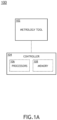
- FIG. 1A is a conceptual view of an overlay metrology system 100 suitable for device-correlated metrology measurements, in accordance with one or more embodiments of the present disclosure.
- the overlay metrology system 100 include at least one overlay metrology tool 102 suitable for measuring intra-layer pattern placement distances as well as inter-layer overlay measurements of stacked overlay target features.
- the overlay metrology system 100 includes a controller 104.
- the controller 104 includes one or more processors 106 configured to execute program instructions maintained on a memory medium 108.
- the one or more processors 106 of controller 104 may execute any of the various process steps described throughout the present disclosure.
- the controller 104 may receive data from the overlay metrology tool 102 and may further generate device-correlated overlay data.
- the controller 104 may generate device-relevant overlay correctables based on data from the overlay metrology tool 102.
- controller 104 may be communicatively coupled to one or more external fabrication tools such as, but not limited to, a lithography tool.
- controller 104 may operate as an advanced process controller (APC) suitable for controlling the inputs of the external fabrication tools to maintain overlay within selected overlay tolerances.
- API advanced process controller
- the one or more processors 106 of a controller 104 may include any processing element known in the art. In this sense, the one or more processors 106 may include any microprocessor-type device configured to execute algorithms and/or instructions. In one embodiment, the one or more processors 106 may consist of a desktop computer, mainframe computer system, workstation, image computer, parallel processor, or any other computer system (e.g., networked computer) configured to execute a program configured to operate the overlay metrology system 100, as described throughout the present disclosure. It is further recognized that the term "processor" may be broadly defined to encompass any device having one or more processing elements, which execute program instructions from a non-transitory memory medium 108.
- controller 104 may include one or more controllers housed in a common housing or within multiple housings. In this way, any controller or combination of controllers may be separately packaged as a module suitable for integration into overlay metrology system 100.
- the memory medium 108 may include any storage medium known in the art suitable for storing program instructions executable by the associated one or more processors 106.
- the memory medium 108 may include a non-transitory memory medium.
- the memory medium 108 may include, but is not limited to, a read-only memory (ROM), a random-access memory (RAM), a magnetic or optical memory device (e.g., disk), a magnetic tape, a solid-state drive, and the like. It is further noted that memory medium 108 may be housed in a common controller housing with the one or more processors 106. In one embodiment, the memory medium 108 may be located remotely with respect to the physical location of the one or more processors 106 and controller 104.
- controller 104 may access a remote memory (e.g., server), accessible through a network (e.g., internet, intranet, and the like). Therefore, the above description should not be interpreted as a limitation on the present invention but merely an illustration.
- a remote memory e.g., server
- a network e.g., internet, intranet, and the like.
- the overlay metrology tool 102 may include any type of metrology tool known in the art suitable for characterizing intra-layer pattern placement distances and/or inter-layer overlay measurements.
- the overlay metrology tool 102 may illuminate a sample with an illumination beam and may further collect radiation emanating from the sample in response to the illumination beam.
- the illumination beam may include any type of illumination beam suitable for probing a sample such as, but not limited to, a light beam (e.g., photons), an electron beam, or an ion beam.
- the radiation emanating from the sample may include photons, electrons, ions, neutral particles, or the like.
- the overlay metrology tool 102 may include an optical metrology tool, an e-beam metrology tool, an ion-beam metrology tool, or the like.
- the overlay metrology tool 102 may further operate in either an imaging mode or a non-imaging mode.
- the overlay metrology tool 102 operating in an imaging mode may illuminate a portion of the sample larger than the system resolution and capture one or more images of the illuminated portion of the sample on a detector.
- the captured image may be any type of image known in the art such as, but not limited to, a brightfield image, a darkfield image, a phase-contrast image, or the like.
- captured images may be stitched together (e.g., by the controller 104, or the like) to form a composite image of the sample.
- the overlay metrology tool 102 may generate multiple images of the sample using multiple detectors either simultaneously or sequentially.
- the overlay metrology tool 102 may generate images of the sample from different perspectives.
- the overlay metrology tool 102 may generate images of the sample using different beam energies (e.g., particle beam energies, optical intensities, wavelengths, or the like).
- the overlay metrology tool 102 may scan a focused beam across the sample and capture radiation and/or particles emanating from the sample on one or more detectors at one or more measurement angles to generate the image.
- the focused beam may be scanned across the sample by modifying the beam path and/or by translating the sample through a focal volume of the focused beam.
- particle beams may be scanned using controlled electromagnetic fields (e.g., generated using one or more beam deflectors, or the like).
- light beams may be scanned using scanning mirrors (e.g., galvo mirrors, piezo-electric mirrors, or the like).
- the overlay metrology tool 102 may include, but is not required to include, a particle-based overlay metrology tool 102a and/or an optical overlay metrology tool 102b.
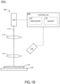
- FIG. 1B is a conceptual view of a particle-based overlay metrology tool 102a, in accordance with one or more embodiments of the present disclosure.
- the particle-based overlay metrology tool 102a may include any type of metrology tool suitable for resolving device features or device-scale features such as, but not limited to an electron-beam metrology tool (e.g., a SEM, a CD-SEM, or the like), or an ion-beam metrology tool (e.g., a focused-ion-beam (FIB) metrology tool.
- an electron-beam metrology tool e.g., a SEM, a CD-SEM, or the like
- an ion-beam metrology tool e.g., a focused-ion-beam (FIB) metrology tool.
- FIB focused-ion-beam
- the particle-based overlay metrology tool 102a a particle source 110 (e.g., an electron beam source, an ion beam source, or the like) to generate a particle beam 112 (e.g., an electron beam, a particle beam, or the like).
- the particle source 110 may include any particle source known in the art suitable for generating a particle beam 112.
- the particle source 110 may include, but is not limited to, an electron gun or an ion gun.
- the particle source 110 is configured to provide a particle beam with a tunable energy.
- particle source 110 including an electron source may, but is not limited to, provide an accelerating voltage in the range of 0.1 kV to 30 kV.
- a particle source 110 including an ion source may, but is not required to, provide an ion beam with an energy in the range of 1 to 50 keV.
- the particle-based overlay metrology tool 102a includes one or more particle focusing elements 114.
- the one or more particle focusing elements 114 may include, but are not limited to, a single particle focusing element or one or more particle focusing elements forming a compound system.
- the one or more particle focusing elements 114 include a particle objective lens 116 configured to direct the particle beam 112 to a sample 118 located on a sample stage 120.
- the one or more particle source 110 may include any type of electron lenses known in the art including, but not limited to, electrostatic, magnetic, uni-potential, or double-potential lenses.
- the particle-based overlay metrology tool 102a includes at least one particle detector 122 to image or otherwise detect particles emanating from the sample 118.
- the particle detector 122 includes an electron collector (e.g., a secondary electron collector, a backscattered electron detector, or the like).
- the particle detector 122 includes a photon detector (e.g., a photodetector, an x-ray detector, a scintillating element coupled to photomultiplier tube (PMT) detector, or the like) for detecting electrons and/or photons from the sample surface.
- PMT photomultiplier tube
- the description of a particle-based overlay metrology tool 102a as depicted in FIG. 1B and the associated descriptions above are provided solely for illustrative purposes and should not be interpreted as limiting.
- the particle-based overlay metrology tool 102a may include a multi-beam and/or a multi-column system suitable for simultaneously interrogating a sample 118.
- the particle-based overlay metrology tool 102a may include one or more components (e.g., one or more electrodes) configured to apply one or more voltages to one or more locations of the sample 118.
- the particle-based overlay metrology tool 102a may generate voltage contrast imaging data.
- the penetration depth of the particle beam 112 in the sample 118 may depend on the particle energy such that higher-energy beams typically penetrate deeper into the sample.
- the particle-based overlay metrology tool 102a utilizes different particle energies to interrogate different layers of the device based on the penetration depth of the particle beam 112 into the sample 118.
- the particle-based overlay metrology tool 102a may utilize a relatively low-energy electron beam (e.g., approximately 1 keV or less) and may utilize a higher energy beam (e.g., approximately 10 keV or higher) to characterize a previously fabricated layer.
- the penetration depth as a function of particle energy may vary for different materials such that the selection of the particle energy for a particular layer may vary for different materials.
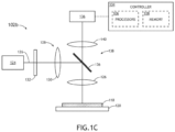
- FIG. 1C is a conceptual view of an optical overlay metrology tool 102b, in accordance with one or more embodiments of the present disclosure.
- the optical overlay metrology tool 102b may include any type of optical overlay metrology tool known in the art suitable for generating overlay data associated with two or more layers of a sample.
- the optical overlay metrology tool 102b includes an optical illumination source 124 to generate an optical illumination beam 126.
- the optical illumination beam 126 may include one or more selected wavelengths of light including, but not limited to, ultraviolet (UV) light, visible light, or infrared (IR) light.
- the optical illumination source 124 may be any type of illumination source known in the art suitable for generating an optical illumination beam 126.
- the optical illumination source 124 may include any type of illumination source suitable for providing an optical illumination beam 126.
- the optical illumination source 124 is a laser source.
- the optical illumination source 124 may include, but is not limited to, one or more narrowband laser sources, a broadband laser source, a supercontinuum laser source, a white light laser source, or the like.
- the optical illumination source 124 may provide an optical illumination beam 126 having high coherence (e.g., high spatial coherence and/or temporal coherence).
- the optical illumination source 124 includes a laser-sustained plasma (LSP) source.
- LSP laser-sustained plasma
- the optical illumination source 124 may include, but is not limited to, a LSP lamp, a LSP bulb, or a LSP chamber suitable for containing one or more elements that, when excited by a laser source into a plasma state, may emit broadband illumination.
- the optical illumination source 124 includes a lamp source.
- the optical illumination source 124 may include, but is not limited to, an arc lamp, a discharge lamp, an electrode-less lamp, or the like.
- the optical illumination source 124 may provide an optical illumination beam 126 having low coherence (e.g., low spatial coherence and/or temporal coherence).
- the optical illumination source 124 directs the optical illumination beam 126 to a sample 118 via an illumination pathway 128.
- the illumination pathway 128 may include one or more illumination pathway lenses 130 or additional optical components 132 suitable for modifying and/or conditioning the optical illumination beam 126.
- the one or more optical components 132 may include, but are not limited to, one or more polarizers, one or more filters, one or more beam splitters, one or more diffusers, one or more homogenizers, one or more apodizers, or one or more beam shapers.
- the illumination pathway 128 may further include an objective lens 134 configured to direct the optical illumination beam 126 to the sample 118.
- the sample 118 is disposed on a sample stage 120.
- the sample stage 120 may include any device suitable for positioning and/or scanning the sample 118 within the optical overlay metrology tool 102b.
- the sample stage 120 may include any combination of linear translation stages, rotational stages, tip/tilt stages, or the like.
- the optical overlay metrology tool 102b includes a detector 136 configured to capture light emanating from the sample 118 through a collection pathway 138.
- the collection pathway 138 may include, but is not limited to, one or more collection pathway lenses 140 for collecting light from the sample 118.
- a detector 136 may receive light reflected or scattered (e.g., via specular reflection, diffuse reflection, and the like) from the sample 118 via one or more collection pathway lenses 140.
- a detector 136 may receive light generated by the sample 118 (e.g., luminescence associated with absorption of the optical illumination beam 126, or the like).
- a detector 136 may receive one or more diffracted orders of light from the sample 118 (e.g., 0-order diffraction, ⁇ 1 order diffraction, ⁇ 2 order diffraction, and the like).
- the detector 136 may include any type of detector known in the art suitable for measuring illumination received from the sample 118.
- a detector 136 may include, but is not limited to, a CCD detector, a TDI detector, a photomultiplier tube (PMT), an avalanche photodiode (APD), or the like.
- a detector 136 may include a spectroscopic detector suitable for identifying wavelengths of light emanating from the sample 118.
- the collection pathway 138 may further include any number of optical elements to direct and/or modify collected illumination from the sample 118 including, but not limited to one or more collection pathway lenses 140, one or more filters, one or more polarizers, or one or more beam blocks.
- the detector 136 is positioned approximately normal to the surface of the sample 118.
- the optical overlay metrology tool 102b includes a beamsplitter 142 oriented such that the objective lens 134 may simultaneously direct the optical illumination beam 126 to the sample 118 and collect light emanating from the sample 118. Further, the illumination pathway 128 and the collection pathway 138 may share one or more additional elements (e.g., objective lens 134, apertures, filters, or the like).
- the optical overlay metrology tool 102b may measure overlay based on any technique known in the art such as, but not limited to, imaged-based techniques or scatterometry-based techniques. Further, the optical overlay metrology tool 102b may measure overlay based on features on any layer of the sample 118 by having the optical illumination beam 126 propagate through a surface layer to interact with features on one or more previously fabricated layers.
- the overlay metrology tool 102 includes an edge-placement metrology tool suitable for measurements of the pattern placement distances (or pattern placement errors) of various features on a sample layer.
- the position of the sample stage 120 may be tightly monitored to provide accurate positioning results over a large field of view.
- positioning accuracy based on monitoring actual positions of the sample stage 120 as opposed to positioning accuracy based solely on control of the sample stage 120 itself, may be limited only by the monitoring accuracy.
- the position of the sample stage 120 along one or more directions is monitored using an interferometer, which may provide, but is not required to provide, nanometer or sub-nanometer accuracy.
- the overlay metrology tool 102 including an edge-placement metrology tool may be based on any type of imaging technology such as, but not limited to, optical or particle-beam imaging.
- imaging technology such as, but not limited to, optical or particle-beam imaging.
- the measurement of the positions and dimensions of structures using edge-placement metrology is generally described in Int'l Pub. No. WO 2018/004511 titled “APPARATUS AND METHOD FOR THE MEASUREMENT OF PATTERN PLACEMENT AND SIZE OF PATTERN AND COMPUTER PROGRAM THEREFOR” and published on January 4, 2018 , and U.S. Patent No. 9,704,238 titled “METHOD FOR CORRECTING POSITION MEASUREMENTS FOR OPTICAL ERRORS AND METHOD FOR DETERMINING MASK WRITER ERRORS” and issued on July 11, 2017 .
- the overlay metrology system 100 includes multiple overlay metrology tools 102.
- the overlay metrology system 100 may include a first overlay metrology tool 102 suitable for measuring intra-layer pattern placement distances of device-scale features and a second overlay metrology system 100 suitable for measuring inter-layer overlay.
- the multiple overlay metrology tools 102 may have different operational principles.
- an overlay metrology tool 102 suitable for measuring intra-layer pattern placement distances of device-scale features may include a particle-based metrology tool having sufficient resolution to resolve device-scale features.
- an overlay metrology tool 102 suitable for measuring inter-layer overlay may include either a particle-based metrology tool or an optical metrology tool.
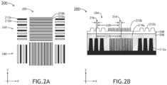
- FIG. 2A includes a top view 202 of a device-correlated overlay target 200, in accordance with one or more embodiments of the present disclosure.
- FIG. 2B includes a profile view 204 of a device-correlated overlay target 200, in accordance with one or more embodiments of the present disclosure.
- the device-correlated overlay target 200 includes features on multiple layers of the sample 118.
- the device-correlated overlay target 200 may include features on a first layer 206 and a second layer 208 fabricated on top of and subsequent to the first layer 206.
- the device-correlated overlay target 200 includes both device-scale features and reference features on each layer of interest.
- the device-correlated overlay target 200 may include first-layer pattern of device-scale features 210a and a second-layer pattern of device-scale features 210b.
- the device-correlated overlay target 200 may include a first-layer pattern of reference features 212a and a second-layer pattern of reference features 212b.
- the device-correlated overlay target 200 includes stacked (e.g., overlapping) patterns.
- the second-layer pattern of device-scale features 210b may be stacked on the first-layer pattern of device-scale features 210a such that a device-correlated overlay 214 may correspond to a relative displacement of the second-layer pattern of device-scale features 210b with respect to the first-layer pattern of device-scale features 210a.
- the second-layer pattern of reference features 212b may be stacked on the first-layer pattern of reference features 212a such that a reference overlay 216 may correspond to a relative displacement of the second-layer pattern of reference features 212b with respect to the first-layer pattern of reference features 212a.
- the first layer 206 and the second layer 208 include the same feature patterns.
- the first-layer pattern of device-scale features 210a may be substantially the same as the second-layer pattern of device-scale features 210b across the device-correlated overlay target 200.
- the first-layer pattern of reference features 212a may be substantially the same as the second-layer pattern of reference features 212b across the device-correlated overlay target 200.
- the first layer 206 and the second layer 208 include different feature patterns. For example, features on the second layer 208 may be fabricated with a different period than features on the first layer 206.
- features in the second layer 208 may be fabricated with twice the period of features on the first layer 206 (e.g., the first-layer pattern of device-scale features 210a and the first-layer pattern of reference features 212a).
- the features on the first layer may be alternately visible or covered in the top view 202.
- the first-layer pattern of device-scale features 210a and the second-layer pattern of device-scale features 210b may be fabricated with different characteristics such as, but not limited to, feature dimensions, (e.g., critical dimensions, lengths, widths, and/or heights), sidewall angles, or orientations.
- feature dimensions e.g., critical dimensions, lengths, widths, and/or heights
- sidewall angles e.g., sidewall angles, or orientations.
- device-scale features are fabricated at a nominal selected distance (e.g., pattern placement distance) from the reference features.
- a nominal selected distance e.g., pattern placement distance
- intra-field errors can lead to variations in the relative placement of the device-scale features and the reference features.
- a first-layer pattern placement distance 218 associated with a separation between selected portions of the first-layer pattern of device-scale features 210a and the first-layer pattern of reference features 212a may differ from a second-layer pattern placement distance 220 associated with a separation between selected portions of the second-layer pattern of device-scale features 210b and the second-layer pattern of reference features 212b.
- the device-correlated overlay 214 may be characterized in terms of the reference overlay 216 ( OVL ref ) and the PPE associated with a difference between the first-layer pattern placement distance 218 and the second-layer pattern placement distance 220.
- the pattern placement distances may be determined using any technique known in the art.
- the pattern placement distances may be determined by analyzing (e.g., with the controller 104) an image of at least a portion of the device-correlated overlay target 200 generated with a particle-based metrology tool (e.g., particle-based overlay metrology tool 102a) with a resolution sufficient to resolve the device-scale features.
- a particle-based metrology tool e.g., particle-based overlay metrology tool 102a
- the reference overlay 216 may be determined using any technique known in the art.
- the reference overlay 216 may be determined by analyzing (e.g., with the controller 104) an image of at least a portion of the device-correlated overlay target 200 generated with a particle-based metrology tool (e.g., particle-based overlay metrology tool 102a) with a resolution sufficient to resolve the reference features.
- the reference overlay 216 may be determined using an optical metrology tool (e.g., optical overlay metrology tool 102b).
- the controller 104 may analyze an optical image of the reference features on multiple layers of interest.
- the controller 104 may determine the reference overlay 216 using a model-based analysis of a diffraction pattern associated with interaction of an optical illumination beam 126 with both the first-layer pattern of reference features 212a and the second-layer pattern of reference features 212b.
- a pattern of reference features may be periodically distributed along a scan direction.
- the repeated reference features may provide multiple measurement points for the reference overlay 216 along the scan direction, which may reduce stochastic measurement noise compared to a single measurement and thus increase the measurement accuracy.
- repeated reference features may reduce a dose on the sample during an overlay measurement (e.g., associated with a particle beam 112, an optical illumination beam 126, or the like) required to generate an overlay measurement of a selected precision. Further, reducing the dose required for an overlay measurement may mitigate charging effects as well as resist shrinkage effects, which may further increase the measurement precision
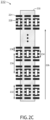
- FIG. 2C is a top view 222 of periodically-distributed reference features of an overlay target (e.g., device-correlated overlay target 200, or the like) suitable for scanning measurements, in accordance with one or more embodiments of the present disclosure.
- periodically distributed first-layer features 224 are located on a first layer of a sample (e.g., sample 118) along a scanning direction 226.
- periodically-distributed second-layer features 228 are located on a second layer of the sample along the scanning direction 226. Further, as illustrated in FIG.
- the second-layer features 228 may be stacked on the first-layer features 224 such that a swath 230 of an imaging beam (e.g., a particle beam 112, an optical illumination beam 126, or the like) may simultaneously image both the first-layer features 224 and the second-layer features 228.
- an imaging beam e.g., a particle beam 112, an optical illumination beam 126, or the like
- the reference features may have dimensions selected to be greater than a resolution of a selected overlay metrology tool (e.g., the particle-based overlay metrology tool 102a, the optical overlay metrology tool 102b, or the like) such that the features may be resolved by the overlay metrology tool.
- a length 232 of first-layer features 224 along the scanning direction 226, a length 234 of second-layer features 228 along the scanning direction 226, and/or the pitch 236 along the scanning direction 226 may be selected such that the first-layer features 224 and the second-layer features 228 are resolvable with the selected overlay metrology tool.
- the reference features on any layer may be further segmented.
- the reference features on all layers of the overlay target may be periodically distributed with a resolvable pitch 236 and reference features on any layer of the target may be further segmented with a device-scale pitch 238 to provide process-compatibility with design rules of the layer and minimize systematic placement errors between the reference features and device features on the layer.
- the resolution of a particle-based overlay metrology tool 102a may be lower for sub-surface features (e.g., first-layer features 224) relative to surface-level features (e.g., second-layer features 228) such that the segments separated with the device-scale pitch 238 may not be resolvable with the overlay metrology tool.
- the reference overlay 216 may be measured.
- the device-correlated overlay target 200 may be further configured to facilitate overlay measurements in multiple directions.
- the profile view 204 illustrates the determination of overlay along the X-direction.
- the device-correlated overlay target 200 includes a first set of features 240 oriented along the X-direction suitable for overlay measurements along the X-direction and a second set of features 242 oriented along the Y-direction suitable for overlay measurements along the Y-direction.
- a device-correlated overlay target may additionally include multiple sets of different device-scale feature patterns and/or multiple sets of different reference feature patterns.
- an overlay target is referred to as a composite overlay target.
- a fabricated layer may include device features (e.g., forming part of a semiconductor device) with varying dimensions, densities, and/or orientations. Accordingly, the varying dimensions, densities and/or orientations of the device features may lead to varying pattern placement error and thus varying on-device overlay.
- a composite device-correlated overlay target may include different device-scale feature patterns to correspond to different device structures on a given layer. In this regard, device-correlated overlay may be measured for each type of device-scale feature pattern to facilitate robust and accurate overlay measurements for multiple device structures.
- a composite device-correlated overlay target may include multiple sets of reference feature patterns.
- overlay may be measured based on any selected combination of device-scale feature patterns and reference feature patterns.
- FIG. 3 is a conceptual view of a composite device-correlated overlay target 300, in accordance with one or more embodiments of the present disclosure.
- the composite device-correlated overlay target 300 includes multiple device-scale patterns 302a-g.
- the composite device-correlated overlay target 300 includes multiple reference patterns 304a,b.
- the multiple device-scale patterns 302a-g as well as the multiple reference patterns 304a,b may be distributed in any spatially-separated orientation.
- the composite device-correlated overlay target 300 may be divided into a grid such in which each segment of the grid includes a device-scale pattern and/or a reference pattern.
- a device-correlated overlay measurement may be generated between any device-scale patterns 302a-g and any reference patterns 304a,b.
- a selected device-scale patterns 302a-g and a selected reference patterns 304a,b may be considered in combination as a device-correlated overlay target (e.g., similar to the device-correlated overlay target 200 illustrated in FIG. 3 , but not limited to the specific design illustrated in FIG. 3 ).
- a device-correlated overlay measurement may be generated based on equation 1 and the illustrative description of the device-correlated overlay target 200 of FIG. 3 .
- the device-scale patterns 302a-g and the reference patterns 304a,b may include features oriented along any direction.
- each device-scale patterns 302a-g or the reference patterns 304a,b may include features distributed along multiple directions suitable for the determination of overlay along the multiple directions.
- device-scale patterns 302a-g or the reference patterns 304a,b may include features distributed along a single direction.
- a composite device-correlated overlay target may facilitate efficient measurement of device-correlated overlay values for multiple device-scale patterns.
- a single reference overlay measurement e.g., OVL ref
- any of reference patterns 304a,b may be applied to determine multiple device-relevant overlays of multiple device patterns.
- device-correlated overlay measured with different combinations of device-scale patterns and reference patterns may facilitate the determination of systematic fabrication errors such as, but not limited to, aberrations of the lithography system.
- composite device-correlated overlay target 300 illustrated in FIG. 3 is provided solely for illustrative purposes and should not be interpreted as limiting.
- a composite device-correlated overlay target 300 may have any shape suitable for including multiple device-scale feature patterns and/or reference feature patterns such as, but not limited to, a rectangle or a circle.
- FIG. 4 is a flow diagram illustrating steps performed in a method 400 for measuring device-correlated overlay, in accordance with one or more embodiments of the present disclosure. Applicant notes that the embodiments and enabling technologies described previously herein in the context of the overlay metrology system 100 should be interpreted to extend to method 400. It is further noted, however, that the method 400 is not limited to the architecture of the overlay metrology system 100.
- the method 400 includes a step 402 of fabricating a first layer of an overlay target on a sample including at least a pattern of device-scale features and a pattern of reference features.
- an overlay target may include device-scale features that have one or more characteristics (e.g., size, shape, density, orientation, or the like) similar to device features forming a portion of a semiconductor device on the first layer.
- the device-scale features may print with similar characteristics as the device features.
- the overlay target may additionally include reference features having selected characteristics (e.g., size, shape, density, orientation, or the like) suitable for providing inter-layer overlay measurements with corresponding features in subsequent layers. Further, the characteristics of the reference features that may differ, but are not required to differ, from the characteristics of the device-scale features.
- the method 400 includes a step 404 of measuring, with an imaging system subsequent to fabricating the first layer, a first-layer pattern placement distance between the pattern of device-scale features and the pattern of reference features on the first layer.
- the first-layer pattern placement distance may be measured using any technique known in the art.
- the step 404 may include generating one or more images of the device-scale features and the reference features on the first layer and determining the first-layer pattern placement distance based on the one or more images.
- the imaging system used in step 404 is a particle-based imaging system (e.g., particle-based overlay metrology tool 102a, or the like) suitable for resolving the device-scale features.
- a particle-based imaging system e.g., particle-based overlay metrology tool 102a, or the like
- the method 400 includes a step 406 of fabricating a second layer of the overlay target on the sample including at least the pattern of device features and the pattern of reference features.
- the pattern of device-scale features and the pattern of reference features may be duplicated on the second layer.
- the device-scale features on the first and second layers are stacked (e.g., overlapped).
- a device-correlated overlay may be associated with a relative displacement of the device-scale features on the second layer with respect to the first layer.
- the pattern of reference features on the first and second layers may be stacked such that a reference overlay may be associated with a relative displacement of the reference features on the second layer with respect to the first layer.
- the method 400 includes a step 408 of measuring, with the imaging system subsequent to fabricating the second layer, a second-layer pattern placement distance between the pattern of device features and the pattern of reference features on the second layer.
- the step 408 may be substantially similar to the step 404 repeated on the second layer.
- first-layer pattern placement distance and the second-layer pattern placement distance may be measured using the same imaging system to provide consistent measurements.
- the method 400 includes a step 410 of measuring, with an overlay metrology system, a reference overlay based on relative positions of the pattern of reference features on the first layer and the pattern of reference features on the second layer.
- the reference overlay may be measured using any overlay technique known in the art.
- the reference overlay may be measured using a particle-based overlay tool (e.g., particle-based overlay metrology tool 102a, or the like).
- the particle-based overlay metrology tool may utilize different particle energies to interrogate different layers of the device based on the penetration depth of a particle beam into the sample.
- the particle-based overlay metrology tool may utilize a relatively low-energy electron beam (e.g., approximately 1 keV or less) and may utilize a higher energy beam (e.g., approximately 10 keV or higher) to characterize a previously fabricated layer.
- the penetration depth as a function of particle energy may vary for different materials such that the selection of the particle energy for a particular layer may vary for different materials.
- the reference overlay may be measured using optical metrology techniques such as, but not limited to, optical imaging metrology or scatterometry overlay metrology.
- optical metrology techniques may utilize any wavelength of electromagnetic radiation such as, but not limited to, x-ray wavelengths, extreme ultraviolet (EUV) wavelengths, vacuum ultraviolet (VUV) wavelengths, deep ultraviolet (DUV) wavelengths, ultraviolet (UV) wavelengths, visible wavelengths, or infrared (IR) wavelengths.
- EUV extreme ultraviolet
- VUV vacuum ultraviolet
- DUV deep ultraviolet
- UV ultraviolet
- visible wavelengths visible wavelengths
- IR infrared
- the reference features on the first layer and the second layer are periodically distributed along a scan direction.
- the reference overlay may be measured along the scan direction and may provide multiple measurement points for the reference overlay, which may reduce stochastic measurement noise. Accordingly, the dose required to generate the reference overlay measurement may be decreased relative to non-repeating structures, which may mitigate errors associated with the measurement itself such as, but not limited to, charging effects and resist-layer shrinkage.
- the method 400 includes a step 412 of determining a device-relevant overlay for the pattern of device-scale features by adjusting the reference overlay with a difference between the first-layer pattern placement distance and the second-layer pattern placement distance.
- a device-relevant overlay may be characterized in terms of the reference overlay ( OVL ref ) associated with step 410 and the ⁇ PPE associated with a difference between the first-layer pattern placement distance of step 404 and the second-layer pattern placement distance of step 408.
- the method 400 includes a step 414 of providing overlay correctables based on the device-relevant overlay to a lithography system to modify exposure conditions of at least one subsequent exposure.
- step 414 may include generating control parameters (or corrections to the control parameters) for fabrication tools such as, but not limited to, lithography tools based on the device-relevant overlay.
- the control parameters may be generated by a control system such as, but not limited to, the controller 104 of the overlay metrology system 100.
- the overlay correctables may be provided as part of a feedback and/or a feedforward control loop.
- the device-relevant overlay measurements associated with a current process step measured on a sample are used to compensate for drifts of one or more fabrication processes and may thus maintain overlay within selected tolerances across multiple exposures on subsequent samples in the same or different lots.
- the device-relevant overlay measurements associated with a current process step may be fed-forward to adjust subsequent process steps to compensate for any measured overlay errors. For example, the exposure of patterns on subsequent layers may be adjusted to match the measured overlay of the subsequent layers.
- any two components herein combined to achieve a particular functionality can be seen as “associated with” each other such that the desired functionality is achieved, irrespective of architectures or intermedial components.
- any two components so associated can also be viewed as being “connected” or “coupled” to each other to achieve the desired functionality, and any two components capable of being so associated can also be viewed as being “couplable” to each other to achieve the desired functionality.
- Specific examples of couplable include but are not limited to physically interactable and/or physically interacting components and/or wirelessly interactable and/or wirelessly interacting components and/or logically interactable and/or logically interacting components.
Landscapes
- Physics & Mathematics (AREA)
- General Physics & Mathematics (AREA)
- Engineering & Computer Science (AREA)
- Manufacturing & Machinery (AREA)
- Computer Hardware Design (AREA)
- Microelectronics & Electronic Packaging (AREA)
- Power Engineering (AREA)
- Exposure And Positioning Against Photoresist Photosensitive Materials (AREA)
- Testing Or Measuring Of Semiconductors Or The Like (AREA)
- Electromagnetism (AREA)
- Polyamides (AREA)
Applications Claiming Priority (3)
| Application Number | Priority Date | Filing Date | Title |
|---|---|---|---|
| US201762595987P | 2017-12-07 | 2017-12-07 | |
| US16/009,939 US10474040B2 (en) | 2017-12-07 | 2018-06-15 | Systems and methods for device-correlated overlay metrology |
| PCT/US2018/064145 WO2019113262A1 (en) | 2017-12-07 | 2018-12-06 | Systems and methods for device-correlated overlay metrology |
Publications (3)
| Publication Number | Publication Date |
|---|---|
| EP3721294A1 EP3721294A1 (en) | 2020-10-14 |
| EP3721294A4 EP3721294A4 (en) | 2021-09-01 |
| EP3721294B1 true EP3721294B1 (en) | 2025-05-28 |
Family
ID=66696697
Family Applications (1)
| Application Number | Title | Priority Date | Filing Date |
|---|---|---|---|
| EP18886399.7A Active EP3721294B1 (en) | 2017-12-07 | 2018-12-06 | Systems and methods for device-correlated overlay metrology |
Country Status (8)
Families Citing this family (18)
| Publication number | Priority date | Publication date | Assignee | Title |
|---|---|---|---|---|
| US10964566B2 (en) * | 2018-06-29 | 2021-03-30 | Taiwan Semiconductor Manufacturing Go., Ltd. | Machine learning on overlay virtual metrology |
| US11073768B2 (en) | 2019-06-26 | 2021-07-27 | Kla Corporation | Metrology target for scanning metrology |
| US11914290B2 (en) | 2019-07-24 | 2024-02-27 | Kla Corporation | Overlay measurement targets design |
| US11221561B2 (en) * | 2020-01-14 | 2022-01-11 | Kla Corporation | System and method for wafer-by-wafer overlay feedforward and lot-to-lot feedback control |
| CN111458984A (zh) * | 2020-03-13 | 2020-07-28 | 华中科技大学 | 一种套刻标记及测量配置的分步优化方法 |
| KR102630496B1 (ko) | 2020-04-15 | 2024-01-29 | 케이엘에이 코포레이션 | 반도체 디바이스의 오정합을 측정하는 데 유용한 디바이스 스케일 피쳐를 갖는 오정합 타겟 |
| US11300405B2 (en) * | 2020-08-03 | 2022-04-12 | Kla Corporation | Grey-mode scanning scatterometry overlay metrology |
| US11556738B2 (en) * | 2020-10-01 | 2023-01-17 | Kla Corporation | System and method for determining target feature focus in image-based overlay metrology |
| US11460783B2 (en) * | 2021-01-07 | 2022-10-04 | Kla Corporation | System and method for focus control in extreme ultraviolet lithography systems using a focus-sensitive metrology target |
| US11703767B2 (en) | 2021-06-28 | 2023-07-18 | Kla Corporation | Overlay mark design for electron beam overlay |
| US11862524B2 (en) | 2021-06-28 | 2024-01-02 | Kla Corporation | Overlay mark design for electron beam overlay |
| US11720031B2 (en) | 2021-06-28 | 2023-08-08 | Kla Corporation | Overlay design for electron beam and scatterometry overlay measurements |
| US12085385B2 (en) | 2021-10-06 | 2024-09-10 | Kla Corporation | Design-assisted large field of view metrology |
| EP4338009A4 (en) * | 2021-10-21 | 2025-06-04 | KLA Corporation | INDUCED SHIFTS FOR IMPROVED OVERHEATING ERROR METROLOGY |
| EP4202552B1 (en) * | 2021-12-24 | 2024-04-17 | Imec VZW | Method and structure for determining an overlay error |
| US12354970B2 (en) | 2022-04-08 | 2025-07-08 | Nanya Technology Corporation | Semiconductor device structure with overlay mark |
| TWI809931B (zh) * | 2022-04-08 | 2023-07-21 | 南亞科技股份有限公司 | 具有疊對標記之半導體元件結構的製備方法 |
| US12243832B2 (en) | 2022-04-08 | 2025-03-04 | Nanya Technology Corporation | Method for manufacturing semiconductor device structure with overlay marks |
Family Cites Families (29)
| Publication number | Priority date | Publication date | Assignee | Title |
|---|---|---|---|---|
| TW588414B (en) | 2000-06-08 | 2004-05-21 | Toshiba Corp | Alignment method, overlap inspecting method and mask |
| US7068833B1 (en) | 2000-08-30 | 2006-06-27 | Kla-Tencor Corporation | Overlay marks, methods of overlay mark design and methods of overlay measurements |
| US7317531B2 (en) | 2002-12-05 | 2008-01-08 | Kla-Tencor Technologies Corporation | Apparatus and methods for detecting overlay errors using scatterometry |
| US7541201B2 (en) | 2000-08-30 | 2009-06-02 | Kla-Tencor Technologies Corporation | Apparatus and methods for determining overlay of structures having rotational or mirror symmetry |
| US6432591B1 (en) * | 2000-08-30 | 2002-08-13 | Micron Technology, Inc. | Overlay target design method with pitch determination to minimize impact of lens aberrations |
| EP1314198B1 (en) * | 2000-08-30 | 2017-03-08 | KLA-Tencor Corporation | Overlay marks, methods of overlay mark design and methods of overlay measurements |
| US6486954B1 (en) * | 2000-09-01 | 2002-11-26 | Kla-Tencor Technologies Corporation | Overlay alignment measurement mark |
| US20030002043A1 (en) | 2001-04-10 | 2003-01-02 | Kla-Tencor Corporation | Periodic patterns and technique to control misalignment |
| US6949462B1 (en) * | 2002-04-04 | 2005-09-27 | Nanometrics Incorporated | Measuring an alignment target with multiple polarization states |
| US7148959B2 (en) * | 2002-11-01 | 2006-12-12 | Asml Netherlands B.V. | Test pattern, inspection method, and device manufacturing method |
| TW200509355A (en) | 2003-04-08 | 2005-03-01 | Aoti Operating Co Inc | Overlay metrology mark |
| DE10345466A1 (de) | 2003-09-30 | 2005-04-28 | Infineon Technologies Ag | Verfahren zur Erfassung von Plazierungsfehlern von Schaltungsmustern bei der Übertragung mittels einer Maske in Schichten eines Substrats eines Halbleiterwafers |
| US7308368B2 (en) * | 2004-09-15 | 2007-12-11 | Asml Netherlands B.V. | Method and apparatus for vibration detection, method and apparatus for vibration analysis, lithographic apparatus, device manufacturing method, and computer program |
| DE102005046973B4 (de) * | 2005-09-30 | 2014-01-30 | Globalfoundries Inc. | Struktur und Verfahren zum gleichzeitigen Bestimmen einer Überlagerungsgenauigkeit und eines Musteranordnungsfehlers |
| WO2007040855A1 (en) | 2005-09-30 | 2007-04-12 | Advanced Micro Devices, Inc. | Structure and method for simultaneously determining an overlay accuracy and pattern placement error |
| US8181327B2 (en) | 2008-02-08 | 2012-05-22 | Zephyros, Inc | Mechanical method for improving bond joint strength |
| US8214317B2 (en) | 2009-08-17 | 2012-07-03 | Pratt & Whitney Rocketdyne, Inc. | Failure detection system risk reduction assessment |
| US9052709B2 (en) * | 2010-07-30 | 2015-06-09 | Kla-Tencor Corporation | Method and system for providing process tool correctables |
| EP2694983B1 (en) | 2011-04-06 | 2020-06-03 | KLA-Tencor Corporation | Method and system for providing a quality metric for improved process control |
| US9097978B2 (en) | 2012-02-03 | 2015-08-04 | Taiwan Semiconductor Manufacturing Company, Ltd. | Method and apparatus to characterize photolithography lens quality |
| US9188876B2 (en) * | 2012-02-07 | 2015-11-17 | Taiwan Semiconductor Manufacturing Company, Ltd. | Method of determining overlay error and control system for dynamic control of reticle position |
| US8860941B2 (en) * | 2012-04-27 | 2014-10-14 | Taiwan Semiconductor Manufacturing Co., Ltd. | Tool induced shift reduction determination for overlay metrology |
| US9201312B2 (en) | 2013-04-16 | 2015-12-01 | Kla-Tencor Corporation | Method for correcting position measurements for optical errors and method for determining mask writer errors |
| US9214317B2 (en) | 2013-06-04 | 2015-12-15 | Kla-Tencor Corporation | System and method of SEM overlay metrology |
| TWI544288B (zh) * | 2014-04-14 | 2016-08-01 | 台灣積體電路製造股份有限公司 | 疊對度量方法 |
| WO2016124393A1 (en) * | 2015-02-04 | 2016-08-11 | Asml Netherlands B.V. | Metrology method and apparatus, computer program and lithographic system |
| CN106325001B (zh) * | 2015-07-10 | 2019-01-22 | 中芯国际集成电路制造(上海)有限公司 | 套刻精度补偿方法及装置 |
| EP3171396A1 (en) | 2015-11-18 | 2017-05-24 | Nederlandse Organisatie voor toegepast- natuurwetenschappelijk onderzoek TNO | Method of determining an overlay error, manufacturing method and system for manufacturing of a multilayer semiconductor device, and semiconductor device manufactured thereby |
| JP6843160B2 (ja) | 2016-06-27 | 2021-03-17 | ケーエルエー コーポレイション | パターン配置及びパターンサイズ計測装置及び方法、並びにそのためのコンピュータプログラム |
-
2018
- 2018-06-15 US US16/009,939 patent/US10474040B2/en active Active
- 2018-12-04 TW TW107143359A patent/TWI781259B/zh active
- 2018-12-06 SG SG11202002413UA patent/SG11202002413UA/en unknown
- 2018-12-06 WO PCT/US2018/064145 patent/WO2019113262A1/en active IP Right Grant
- 2018-12-06 KR KR1020207019440A patent/KR102435141B1/ko active Active
- 2018-12-06 JP JP2020531119A patent/JP7118152B2/ja active Active
- 2018-12-06 EP EP18886399.7A patent/EP3721294B1/en active Active
- 2018-12-06 CN CN201880077786.3A patent/CN111433676B/zh active Active
Also Published As
| Publication number | Publication date |
|---|---|
| CN111433676A (zh) | 2020-07-17 |
| KR20200086748A (ko) | 2020-07-17 |
| KR102435141B1 (ko) | 2022-08-22 |
| US20190179231A1 (en) | 2019-06-13 |
| CN111433676B (zh) | 2022-08-05 |
| TW201935148A (zh) | 2019-09-01 |
| EP3721294A4 (en) | 2021-09-01 |
| JP7118152B2 (ja) | 2022-08-15 |
| TWI781259B (zh) | 2022-10-21 |
| US10474040B2 (en) | 2019-11-12 |
| EP3721294A1 (en) | 2020-10-14 |
| JP2021505959A (ja) | 2021-02-18 |
| SG11202002413UA (en) | 2020-06-29 |
| WO2019113262A1 (en) | 2019-06-13 |
Similar Documents
| Publication | Publication Date | Title |
|---|---|---|
| EP3721294B1 (en) | Systems and methods for device-correlated overlay metrology | |
| EP3762780B1 (en) | Metrology and control of overlay and edge placement errors | |
| US10473460B2 (en) | Overlay measurements of overlapping target structures based on symmetry of scanning electron beam signals | |
| US11809090B2 (en) | Composite overlay metrology target | |
| US11209737B1 (en) | Performance optimized scanning sequence for eBeam metrology and inspection | |
| US20240035812A1 (en) | Metrology target for one-dimensional measurement of periodic misregistration | |
| US20240094639A1 (en) | High-resolution evaluation of optical metrology targets for process control |
Legal Events
| Date | Code | Title | Description |
|---|---|---|---|
| STAA | Information on the status of an ep patent application or granted ep patent |
Free format text: STATUS: THE INTERNATIONAL PUBLICATION HAS BEEN MADE |
|
| PUAI | Public reference made under article 153(3) epc to a published international application that has entered the european phase |
Free format text: ORIGINAL CODE: 0009012 |
|
| STAA | Information on the status of an ep patent application or granted ep patent |
Free format text: STATUS: REQUEST FOR EXAMINATION WAS MADE |
|
| 17P | Request for examination filed |
Effective date: 20200703 |
|
| AK | Designated contracting states |
Kind code of ref document: A1 Designated state(s): AL AT BE BG CH CY CZ DE DK EE ES FI FR GB GR HR HU IE IS IT LI LT LU LV MC MK MT NL NO PL PT RO RS SE SI SK SM TR |
|
| AX | Request for extension of the european patent |
Extension state: BA ME |
|
| DAV | Request for validation of the european patent (deleted) | ||
| DAX | Request for extension of the european patent (deleted) | ||
| A4 | Supplementary search report drawn up and despatched |
Effective date: 20210729 |
|
| RIC1 | Information provided on ipc code assigned before grant |
Ipc: G03F 7/20 20060101AFI20210723BHEP Ipc: H01L 21/66 20060101ALI20210723BHEP Ipc: H01L 23/544 20060101ALI20210723BHEP |
|
| P01 | Opt-out of the competence of the unified patent court (upc) registered |
Effective date: 20230526 |
|
| GRAP | Despatch of communication of intention to grant a patent |
Free format text: ORIGINAL CODE: EPIDOSNIGR1 |
|
| STAA | Information on the status of an ep patent application or granted ep patent |
Free format text: STATUS: GRANT OF PATENT IS INTENDED |
|
| INTG | Intention to grant announced |
Effective date: 20241223 |
|
| GRAS | Grant fee paid |
Free format text: ORIGINAL CODE: EPIDOSNIGR3 |
|
| GRAA | (expected) grant |
Free format text: ORIGINAL CODE: 0009210 |
|
| STAA | Information on the status of an ep patent application or granted ep patent |
Free format text: STATUS: THE PATENT HAS BEEN GRANTED |
|
| AK | Designated contracting states |
Kind code of ref document: B1 Designated state(s): AL AT BE BG CH CY CZ DE DK EE ES FI FR GB GR HR HU IE IS IT LI LT LU LV MC MK MT NL NO PL PT RO RS SE SI SK SM TR |
|
| REG | Reference to a national code |
Ref country code: GB Ref legal event code: FG4D |
|
| REG | Reference to a national code |
Ref country code: CH Ref legal event code: EP |
|
| REG | Reference to a national code |
Ref country code: IE Ref legal event code: FG4D Ref country code: DE Ref legal event code: R096 Ref document number: 602018082316 Country of ref document: DE |
|
| REG | Reference to a national code |
Ref country code: NL Ref legal event code: FP |