EP3712933A1 - Semiconductor module and method for manufacturing same - Google Patents
Semiconductor module and method for manufacturing same Download PDFInfo
- Publication number
- EP3712933A1 EP3712933A1 EP19753674.1A EP19753674A EP3712933A1 EP 3712933 A1 EP3712933 A1 EP 3712933A1 EP 19753674 A EP19753674 A EP 19753674A EP 3712933 A1 EP3712933 A1 EP 3712933A1
- Authority
- EP
- European Patent Office
- Prior art keywords
- insulated substrate
- average roughness
- derived
- semiconductor module
- substrate
- Prior art date
- Legal status (The legal status is an assumption and is not a legal conclusion. Google has not performed a legal analysis and makes no representation as to the accuracy of the status listed.)
- Pending
Links
Images


Classifications
-
- H—ELECTRICITY
- H10—SEMICONDUCTOR DEVICES; ELECTRIC SOLID-STATE DEVICES NOT OTHERWISE PROVIDED FOR
- H10W—GENERIC PACKAGES, INTERCONNECTIONS, CONNECTORS OR OTHER CONSTRUCTIONAL DETAILS OF DEVICES COVERED BY CLASS H10
- H10W76/00—Containers; Fillings or auxiliary members therefor; Seals
- H10W76/40—Fillings or auxiliary members in containers, e.g. centering rings
- H10W76/42—Fillings
- H10W76/47—Solid or gel fillings
-
- C—CHEMISTRY; METALLURGY
- C04—CEMENTS; CONCRETE; ARTIFICIAL STONE; CERAMICS; REFRACTORIES
- C04B—LIME, MAGNESIA; SLAG; CEMENTS; COMPOSITIONS THEREOF, e.g. MORTARS, CONCRETE OR LIKE BUILDING MATERIALS; ARTIFICIAL STONE; CERAMICS; REFRACTORIES; TREATMENT OF NATURAL STONE
- C04B37/00—Joining burned ceramic articles with other burned ceramic articles or other articles by heating
- C04B37/02—Joining burned ceramic articles with other burned ceramic articles or other articles by heating with metallic articles
- C04B37/023—Joining burned ceramic articles with other burned ceramic articles or other articles by heating with metallic articles characterised by the interlayer used
- C04B37/026—Joining burned ceramic articles with other burned ceramic articles or other articles by heating with metallic articles characterised by the interlayer used consisting of metals or metal salts
-
- H—ELECTRICITY
- H05—ELECTRIC TECHNIQUES NOT OTHERWISE PROVIDED FOR
- H05K—PRINTED CIRCUITS; CASINGS OR CONSTRUCTIONAL DETAILS OF ELECTRIC APPARATUS; MANUFACTURE OF ASSEMBLAGES OF ELECTRICAL COMPONENTS
- H05K1/00—Printed circuits
- H05K1/02—Details
- H05K1/03—Use of materials for the substrate
- H05K1/0306—Inorganic insulating substrates, e.g. ceramic, glass
-
- H—ELECTRICITY
- H05—ELECTRIC TECHNIQUES NOT OTHERWISE PROVIDED FOR
- H05K—PRINTED CIRCUITS; CASINGS OR CONSTRUCTIONAL DETAILS OF ELECTRIC APPARATUS; MANUFACTURE OF ASSEMBLAGES OF ELECTRICAL COMPONENTS
- H05K3/00—Apparatus or processes for manufacturing printed circuits
- H05K3/22—Secondary treatment of printed circuits
- H05K3/28—Applying non-metallic protective coatings
- H05K3/281—Applying non-metallic protective coatings by means of a preformed insulating foil
-
- H—ELECTRICITY
- H05—ELECTRIC TECHNIQUES NOT OTHERWISE PROVIDED FOR
- H05K—PRINTED CIRCUITS; CASINGS OR CONSTRUCTIONAL DETAILS OF ELECTRIC APPARATUS; MANUFACTURE OF ASSEMBLAGES OF ELECTRICAL COMPONENTS
- H05K3/00—Apparatus or processes for manufacturing printed circuits
- H05K3/22—Secondary treatment of printed circuits
- H05K3/28—Applying non-metallic protective coatings
- H05K3/284—Applying non-metallic protective coatings for encapsulating mounted components
-
- H—ELECTRICITY
- H10—SEMICONDUCTOR DEVICES; ELECTRIC SOLID-STATE DEVICES NOT OTHERWISE PROVIDED FOR
- H10W—GENERIC PACKAGES, INTERCONNECTIONS, CONNECTORS OR OTHER CONSTRUCTIONAL DETAILS OF DEVICES COVERED BY CLASS H10
- H10W40/00—Arrangements for thermal protection or thermal control
- H10W40/01—Manufacture or treatment
- H10W40/03—Manufacture or treatment of arrangements for cooling
- H10W40/037—Assembling together parts thereof
-
- H—ELECTRICITY
- H10—SEMICONDUCTOR DEVICES; ELECTRIC SOLID-STATE DEVICES NOT OTHERWISE PROVIDED FOR
- H10W—GENERIC PACKAGES, INTERCONNECTIONS, CONNECTORS OR OTHER CONSTRUCTIONAL DETAILS OF DEVICES COVERED BY CLASS H10
- H10W40/00—Arrangements for thermal protection or thermal control
- H10W40/20—Arrangements for cooling
- H10W40/25—Arrangements for cooling characterised by their materials
- H10W40/255—Arrangements for cooling characterised by their materials having a laminate or multilayered structure, e.g. direct bond copper [DBC] ceramic substrates
-
- H—ELECTRICITY
- H10—SEMICONDUCTOR DEVICES; ELECTRIC SOLID-STATE DEVICES NOT OTHERWISE PROVIDED FOR
- H10W—GENERIC PACKAGES, INTERCONNECTIONS, CONNECTORS OR OTHER CONSTRUCTIONAL DETAILS OF DEVICES COVERED BY CLASS H10
- H10W42/00—Arrangements for protection of devices
- H10W42/121—Arrangements for protection of devices protecting against mechanical damage
-
- H—ELECTRICITY
- H10—SEMICONDUCTOR DEVICES; ELECTRIC SOLID-STATE DEVICES NOT OTHERWISE PROVIDED FOR
- H10W—GENERIC PACKAGES, INTERCONNECTIONS, CONNECTORS OR OTHER CONSTRUCTIONAL DETAILS OF DEVICES COVERED BY CLASS H10
- H10W70/00—Package substrates; Interposers; Redistribution layers [RDL]
- H10W70/60—Insulating or insulated package substrates; Interposers; Redistribution layers
- H10W70/67—Insulating or insulated package substrates; Interposers; Redistribution layers characterised by their insulating layers or insulating parts
- H10W70/69—Insulating materials thereof
- H10W70/692—Ceramics or glasses
-
- H—ELECTRICITY
- H10—SEMICONDUCTOR DEVICES; ELECTRIC SOLID-STATE DEVICES NOT OTHERWISE PROVIDED FOR
- H10W—GENERIC PACKAGES, INTERCONNECTIONS, CONNECTORS OR OTHER CONSTRUCTIONAL DETAILS OF DEVICES COVERED BY CLASS H10
- H10W74/00—Encapsulations, e.g. protective coatings
- H10W74/01—Manufacture or treatment
-
- H—ELECTRICITY
- H10—SEMICONDUCTOR DEVICES; ELECTRIC SOLID-STATE DEVICES NOT OTHERWISE PROVIDED FOR
- H10W—GENERIC PACKAGES, INTERCONNECTIONS, CONNECTORS OR OTHER CONSTRUCTIONAL DETAILS OF DEVICES COVERED BY CLASS H10
- H10W74/00—Encapsulations, e.g. protective coatings
- H10W74/10—Encapsulations, e.g. protective coatings characterised by their shape or disposition
- H10W74/111—Encapsulations, e.g. protective coatings characterised by their shape or disposition the semiconductor body being completely enclosed
- H10W74/114—Encapsulations, e.g. protective coatings characterised by their shape or disposition the semiconductor body being completely enclosed by a substrate and the encapsulations
-
- H—ELECTRICITY
- H10—SEMICONDUCTOR DEVICES; ELECTRIC SOLID-STATE DEVICES NOT OTHERWISE PROVIDED FOR
- H10W—GENERIC PACKAGES, INTERCONNECTIONS, CONNECTORS OR OTHER CONSTRUCTIONAL DETAILS OF DEVICES COVERED BY CLASS H10
- H10W74/00—Encapsulations, e.g. protective coatings
- H10W74/10—Encapsulations, e.g. protective coatings characterised by their shape or disposition
- H10W74/111—Encapsulations, e.g. protective coatings characterised by their shape or disposition the semiconductor body being completely enclosed
- H10W74/127—Encapsulations, e.g. protective coatings characterised by their shape or disposition the semiconductor body being completely enclosed characterised by arrangements for sealing or adhesion
-
- H—ELECTRICITY
- H10—SEMICONDUCTOR DEVICES; ELECTRIC SOLID-STATE DEVICES NOT OTHERWISE PROVIDED FOR
- H10W—GENERIC PACKAGES, INTERCONNECTIONS, CONNECTORS OR OTHER CONSTRUCTIONAL DETAILS OF DEVICES COVERED BY CLASS H10
- H10W76/00—Containers; Fillings or auxiliary members therefor; Seals
- H10W76/10—Containers or parts thereof
- H10W76/12—Containers or parts thereof characterised by their shape
- H10W76/15—Containers comprising an insulating or insulated base
-
- H—ELECTRICITY
- H10—SEMICONDUCTOR DEVICES; ELECTRIC SOLID-STATE DEVICES NOT OTHERWISE PROVIDED FOR
- H10W—GENERIC PACKAGES, INTERCONNECTIONS, CONNECTORS OR OTHER CONSTRUCTIONAL DETAILS OF DEVICES COVERED BY CLASS H10
- H10W76/00—Containers; Fillings or auxiliary members therefor; Seals
- H10W76/10—Containers or parts thereof
- H10W76/12—Containers or parts thereof characterised by their shape
- H10W76/15—Containers comprising an insulating or insulated base
- H10W76/157—Containers comprising an insulating or insulated base having interconnections parallel to the insulating or insulated base
-
- H—ELECTRICITY
- H10—SEMICONDUCTOR DEVICES; ELECTRIC SOLID-STATE DEVICES NOT OTHERWISE PROVIDED FOR
- H10W—GENERIC PACKAGES, INTERCONNECTIONS, CONNECTORS OR OTHER CONSTRUCTIONAL DETAILS OF DEVICES COVERED BY CLASS H10
- H10W90/00—Package configurations
-
- H—ELECTRICITY
- H10—SEMICONDUCTOR DEVICES; ELECTRIC SOLID-STATE DEVICES NOT OTHERWISE PROVIDED FOR
- H10W—GENERIC PACKAGES, INTERCONNECTIONS, CONNECTORS OR OTHER CONSTRUCTIONAL DETAILS OF DEVICES COVERED BY CLASS H10
- H10W99/00—Subject matter not provided for in other groups of this subclass
-
- C—CHEMISTRY; METALLURGY
- C04—CEMENTS; CONCRETE; ARTIFICIAL STONE; CERAMICS; REFRACTORIES
- C04B—LIME, MAGNESIA; SLAG; CEMENTS; COMPOSITIONS THEREOF, e.g. MORTARS, CONCRETE OR LIKE BUILDING MATERIALS; ARTIFICIAL STONE; CERAMICS; REFRACTORIES; TREATMENT OF NATURAL STONE
- C04B2235/00—Aspects relating to ceramic starting mixtures or sintered ceramic products
- C04B2235/70—Aspects relating to sintered or melt-casted ceramic products
- C04B2235/96—Properties of ceramic products, e.g. mechanical properties such as strength, toughness, wear resistance
-
- C—CHEMISTRY; METALLURGY
- C04—CEMENTS; CONCRETE; ARTIFICIAL STONE; CERAMICS; REFRACTORIES
- C04B—LIME, MAGNESIA; SLAG; CEMENTS; COMPOSITIONS THEREOF, e.g. MORTARS, CONCRETE OR LIKE BUILDING MATERIALS; ARTIFICIAL STONE; CERAMICS; REFRACTORIES; TREATMENT OF NATURAL STONE
- C04B2237/00—Aspects relating to ceramic laminates or to joining of ceramic articles with other articles by heating
- C04B2237/30—Composition of layers of ceramic laminates or of ceramic or metallic articles to be joined by heating, e.g. Si substrates
- C04B2237/32—Ceramic
- C04B2237/36—Non-oxidic
- C04B2237/366—Aluminium nitride
-
- C—CHEMISTRY; METALLURGY
- C04—CEMENTS; CONCRETE; ARTIFICIAL STONE; CERAMICS; REFRACTORIES
- C04B—LIME, MAGNESIA; SLAG; CEMENTS; COMPOSITIONS THEREOF, e.g. MORTARS, CONCRETE OR LIKE BUILDING MATERIALS; ARTIFICIAL STONE; CERAMICS; REFRACTORIES; TREATMENT OF NATURAL STONE
- C04B2237/00—Aspects relating to ceramic laminates or to joining of ceramic articles with other articles by heating
- C04B2237/30—Composition of layers of ceramic laminates or of ceramic or metallic articles to be joined by heating, e.g. Si substrates
- C04B2237/40—Metallic
- C04B2237/407—Copper
-
- C—CHEMISTRY; METALLURGY
- C04—CEMENTS; CONCRETE; ARTIFICIAL STONE; CERAMICS; REFRACTORIES
- C04B—LIME, MAGNESIA; SLAG; CEMENTS; COMPOSITIONS THEREOF, e.g. MORTARS, CONCRETE OR LIKE BUILDING MATERIALS; ARTIFICIAL STONE; CERAMICS; REFRACTORIES; TREATMENT OF NATURAL STONE
- C04B2237/00—Aspects relating to ceramic laminates or to joining of ceramic articles with other articles by heating
- C04B2237/50—Processing aspects relating to ceramic laminates or to the joining of ceramic articles with other articles by heating
- C04B2237/52—Pre-treatment of the joining surfaces, e.g. cleaning, machining
-
- H—ELECTRICITY
- H05—ELECTRIC TECHNIQUES NOT OTHERWISE PROVIDED FOR
- H05K—PRINTED CIRCUITS; CASINGS OR CONSTRUCTIONAL DETAILS OF ELECTRIC APPARATUS; MANUFACTURE OF ASSEMBLAGES OF ELECTRICAL COMPONENTS
- H05K2201/00—Indexing scheme relating to printed circuits covered by H05K1/00
- H05K2201/20—Details of printed circuits not provided for in H05K2201/01 - H05K2201/10
- H05K2201/2072—Anchoring, i.e. one structure gripping into another
-
- H—ELECTRICITY
- H10—SEMICONDUCTOR DEVICES; ELECTRIC SOLID-STATE DEVICES NOT OTHERWISE PROVIDED FOR
- H10W—GENERIC PACKAGES, INTERCONNECTIONS, CONNECTORS OR OTHER CONSTRUCTIONAL DETAILS OF DEVICES COVERED BY CLASS H10
- H10W70/00—Package substrates; Interposers; Redistribution layers [RDL]
- H10W70/40—Leadframes
-
- H—ELECTRICITY
- H10—SEMICONDUCTOR DEVICES; ELECTRIC SOLID-STATE DEVICES NOT OTHERWISE PROVIDED FOR
- H10W—GENERIC PACKAGES, INTERCONNECTIONS, CONNECTORS OR OTHER CONSTRUCTIONAL DETAILS OF DEVICES COVERED BY CLASS H10
- H10W72/00—Interconnections or connectors in packages
- H10W72/30—Die-attach connectors
- H10W72/351—Materials of die-attach connectors
- H10W72/352—Materials of die-attach connectors comprising metals or metalloids, e.g. solders
-
- H—ELECTRICITY
- H10—SEMICONDUCTOR DEVICES; ELECTRIC SOLID-STATE DEVICES NOT OTHERWISE PROVIDED FOR
- H10W—GENERIC PACKAGES, INTERCONNECTIONS, CONNECTORS OR OTHER CONSTRUCTIONAL DETAILS OF DEVICES COVERED BY CLASS H10
- H10W72/00—Interconnections or connectors in packages
- H10W72/50—Bond wires
- H10W72/551—Materials of bond wires
-
- H—ELECTRICITY
- H10—SEMICONDUCTOR DEVICES; ELECTRIC SOLID-STATE DEVICES NOT OTHERWISE PROVIDED FOR
- H10W—GENERIC PACKAGES, INTERCONNECTIONS, CONNECTORS OR OTHER CONSTRUCTIONAL DETAILS OF DEVICES COVERED BY CLASS H10
- H10W72/00—Interconnections or connectors in packages
- H10W72/851—Dispositions of multiple connectors or interconnections
- H10W72/874—On different surfaces
- H10W72/884—Die-attach connectors and bond wires
-
- H—ELECTRICITY
- H10—SEMICONDUCTOR DEVICES; ELECTRIC SOLID-STATE DEVICES NOT OTHERWISE PROVIDED FOR
- H10W—GENERIC PACKAGES, INTERCONNECTIONS, CONNECTORS OR OTHER CONSTRUCTIONAL DETAILS OF DEVICES COVERED BY CLASS H10
- H10W74/00—Encapsulations, e.g. protective coatings
-
- H—ELECTRICITY
- H10—SEMICONDUCTOR DEVICES; ELECTRIC SOLID-STATE DEVICES NOT OTHERWISE PROVIDED FOR
- H10W—GENERIC PACKAGES, INTERCONNECTIONS, CONNECTORS OR OTHER CONSTRUCTIONAL DETAILS OF DEVICES COVERED BY CLASS H10
- H10W90/00—Package configurations
- H10W90/701—Package configurations characterised by the relative positions of pads or connectors relative to package parts
-
- H—ELECTRICITY
- H10—SEMICONDUCTOR DEVICES; ELECTRIC SOLID-STATE DEVICES NOT OTHERWISE PROVIDED FOR
- H10W—GENERIC PACKAGES, INTERCONNECTIONS, CONNECTORS OR OTHER CONSTRUCTIONAL DETAILS OF DEVICES COVERED BY CLASS H10
- H10W90/00—Package configurations
- H10W90/701—Package configurations characterised by the relative positions of pads or connectors relative to package parts
- H10W90/731—Package configurations characterised by the relative positions of pads or connectors relative to package parts of die-attach connectors
- H10W90/734—Package configurations characterised by the relative positions of pads or connectors relative to package parts of die-attach connectors between a chip and a stacked insulating package substrate, interposer or RDL
-
- H—ELECTRICITY
- H10—SEMICONDUCTOR DEVICES; ELECTRIC SOLID-STATE DEVICES NOT OTHERWISE PROVIDED FOR
- H10W—GENERIC PACKAGES, INTERCONNECTIONS, CONNECTORS OR OTHER CONSTRUCTIONAL DETAILS OF DEVICES COVERED BY CLASS H10
- H10W90/00—Package configurations
- H10W90/701—Package configurations characterised by the relative positions of pads or connectors relative to package parts
- H10W90/751—Package configurations characterised by the relative positions of pads or connectors relative to package parts of bond wires
- H10W90/753—Package configurations characterised by the relative positions of pads or connectors relative to package parts of bond wires between laterally-adjacent chips
-
- H—ELECTRICITY
- H10—SEMICONDUCTOR DEVICES; ELECTRIC SOLID-STATE DEVICES NOT OTHERWISE PROVIDED FOR
- H10W—GENERIC PACKAGES, INTERCONNECTIONS, CONNECTORS OR OTHER CONSTRUCTIONAL DETAILS OF DEVICES COVERED BY CLASS H10
- H10W90/00—Package configurations
- H10W90/701—Package configurations characterised by the relative positions of pads or connectors relative to package parts
- H10W90/751—Package configurations characterised by the relative positions of pads or connectors relative to package parts of bond wires
- H10W90/754—Package configurations characterised by the relative positions of pads or connectors relative to package parts of bond wires between a chip and a stacked insulating package substrate, interposer or RDL
Definitions
- the present invention relates to: a semiconductor module having a structure in which a semiconductor element is joined to an insulated substrate via a circuit pattern and in which the insulated substrate, the circuit pattern, and the semiconductor element are sealed using a sealing resin; and a method for manufacturing the semiconductor module.
- Patent Document 2 discloses a method for manufacturing a ceramic circuit substrate, the method including forming fine asperities on the surfaces of crystal particles through ion-beam etching in order to increase bonding force with a metal film.
- Patent Document 3 discloses a ceramic member in which a plurality of protrusions having a smaller diameter than the diameter of crystal particles are formed through acidic etching on the surfaces of the crystal particles in order to enhance an anchoring effect.
- Patent Document 4 discloses a ceramic base body provided with a plurality of recesses and protrusions having greater asperities than the average crystal grain diameter, whereby an anchoring effect of a brazing material is enhanced.
- Patent Document 5 indicates that a surface is roughened by bringing abrasive grains into contact with the surface of an aluminum nitride substrate, and the joining strength of a metal circuit foil is increased.
- Patent Document 6 discloses an electronic control device provided with: a circuit substrate; a heat sink on which the circuit substrate is mounted; a lead electrically connected to the circuit substrate; and a sealing resin part that covers the circuit substrate as well as a connection part between the circuit substrate and the lead, the sealing resin part being such that a sealing resin is arranged so that a portion of the lead and a portion of the heat sink are exposed to the outside, wherein, in the surface of the circuit substrate and/or the surface of the heat sink, at least a portion of a site in contact with the sealing resin part is subjected to a roughening process.
- Patent Documents 1 to 5 no consideration is given to surface roughening of the insulated substrate for the purpose of improving bonding strength between the insulated substrate and the sealing resin. Moreover, Patent Document 6 does not specifically disclose the conditions of the roughening process.
- a semiconductor module according to the present invention is provided with:
- Za represents the average roughness.
- Zn represents the difference between the two-dimensional coordinate data and an average value for each n.
- N represents a value obtained by dividing a measured width by a measured pitch; in computation of the roughness for a width of 300 ⁇ m, the pitch is equal to 0.5 ⁇ m, that means N is equal to 600, and in computation of the roughness for a width of 3 ⁇ m, the pitch is equal to 0.005 ⁇ m, that means N is equal to 600.
- the portion where the insulated substrate and the sealing resin are bonded preferably includes a peripheral edge part of the insulated substrate.
- the surface of the insulated substrate in the portion where the insulated substrate and the sealing resin are bonded preferably is such that, in a cross-section of the insulated substrate, the average roughness derived in a 300- ⁇ m-wide range is 2 ⁇ m or less.
- the surface of the insulated substrate in the portion where the insulated substrate and the sealing resin are bonded furthermore preferably is such that, in a cross-section of the insulated substrate, the average roughness derived in a 300- ⁇ m-wide range is 0.7 ⁇ m or greater.
- the insulated substrate is preferably made of a ceramic, and is more preferably composed of aluminum nitride.
- an insulated circuit substrate according to the present invention is provided with:
- the surface of the insulated substrate in the portion where the insulated substrate and the sealing resin are bonded is such that, in a cross-section of the insulated substrate, the average roughness derived in a 300- ⁇ m-wide range is 0.15 ⁇ m or greater, and the average roughness derived in a 3- ⁇ m-wide range is 0.02 ⁇ m or greater.
- This improves the bonding strength between the insulated substrate and the sealing resin, maintains a high bonding strength even under high temperature, and suppresses delamination of the sealing resin. It is therefore possible to improve the durability of the semiconductor module.
- comparatively rough asperities are formed in the surface of the insulated substrate through the wet blasting treatment, and the brazing material is furthermore applied and etched in the surface to which the metal foil is not joined, the surface being where the sealing resin is directly bonded.
- the insulated circuit substrate according to the present invention when it is used as an insulated circuit substrate of a semiconductor module and is sealed using a sealing resin, the bonding strength between the insulated substrate and the sealing resin increases, a high bonding strength is maintained even under high temperature, and delamination of the sealing resin is suppressed. It is therefore possible to improve the durability of the semiconductor module.
- FIG. 1 shows a first embodiment of a semiconductor module to which the present invention is applied.
- the semiconductor module 50 is a power semiconductor module, wherein a circuit pattern 24 is formed on the upper surface of an insulated substrate 23, and a metal sheet 22 having excellent thermal conductivity is joined to the lower surface of the insulated substrate 23.
- An insulated circuit substrate 21 is configured from the insulated substrate 23, the circuit pattern 24, and the metal sheet 22.
- a ceramic substrate in which the main component is, e.g., aluminum nitride, alumina, or silicon nitride is preferably used as the insulated substrate 23.
- a ceramic substrate composed of an aluminum nitride sintered compact is particularly preferred.
- the average crystal grain diameter of the ceramic in the ceramic substrate is preferably 0.5 to 20 ⁇ m, and more preferably 2 to 7 ⁇ m.
- the aluminum nitride sintered compact can be obtained by sintering a molded body composed of an aluminum nitride raw powder having an average particle diameter of 0.1 to 15 ⁇ m.
- the molded body may include a sintering auxiliary agent, an organic binder, etc., as necessary.
- the metal foil is not particularly limited; however, as an example, copper is preferably employed.
- the metal sheet 22 is not particularly limited, provided that the metal sheet 22 has excellent thermal conductivity; however, as an example, a metal sheet made of copper, aluminum, a copper alloy, or an aluminum alloy is used.
- Semiconductor elements 25, 26 are joined on the circuit pattern 24 via solder 29.
- An external terminal 12 is provided upright on the circuit pattern 24 via the solder 29, and the semiconductor elements 25, 26 and the external terminal 12 are connected by the circuit pattern 24 or a bonding wire 27.
- the semiconductor elements 25, 26 are, e.g., insulated gate bipolar transistors (IGBTs) or power metal oxide semiconductor field effect transistors (power MOSFETs).
- IGBTs may be reverse blocking-IGBTs (RB-IGBTs) or reverse conducting-IGBTs (RC-IGBTs).
- the insulated substrate 23, the circuit pattern 24, the semiconductor elements 25, 26, lower portions of the external terminal 12, and the side surfaces of the metal sheet 22 are sealed using a sealing resin 28, with the lower surface of the metal sheet 22 and the upper portion of the external terminal 12 being excluded from sealing.
- the sealing resin 28 is not particularly limited; however, as an example, an epoxy resin, a maleimide resin, a silicone resin, or a liquid crystal polymer is used.
- the sealing resin 28 is bonded to each of the insulated substrate 23, the circuit pattern 24, the semiconductor elements 25, 26, the lower portions of the external terminal 12, and the side surfaces of the metal sheet 22.
- the insulated substrate 23 has a surface 23a that is bonded (adherent) to the sealing resin 28 (referred to as a "sealing-resin-bonded surface” below).
- the sealing-resin-bonded surface 23a is formed as being a peripheral edge part of the insulated substrate 23 so as to surround the outer periphery of the metal sheet 22 and the circuit pattern 24.
- the sealing-resin-bonded surface 23a is formed, in addition to as being the peripheral edge part on the upper-surface side of the insulated substrate 23, it is formed as being the outer-peripheral-side surface of the insulated substrate 23 and as being the peripheral edge part on the lower-surface side of the insulated substrate 23, the peripheral edge part being positioned on the outer periphery of the metal sheet 22.
- FIG. 2 shows another embodiment of a semiconductor module to which the present invention is applied.
- This semiconductor module 50a also is a power semiconductor module, wherein a circuit pattern 24 is formed on the upper surface of an insulated substrate 23, and a metal sheet 22 having excellent thermal conductivity is joined to the lower surface of the insulated substrate 23.
- An insulated circuit substrate 21 is configured from the insulated substrate 23, the circuit pattern 24, and the metal sheet 22.
- a frame-shaped case 13 made of a resin is provided surrounding the insulated circuit substrate 21, and the peripheral edge part of the insulated circuit substrate 21 is anchored to the case 13 via an adhesive 14.
- a lower portion of an external terminal 12 that is bent in an L-shape is integrally molded with the case 13 so as to be exposed to the interior of the case 13 through the case 13, constituting an insert case 11.
- Semiconductor elements 25, 26 are joined on the circuit pattern 24 via solder 29.
- the semiconductor elements 25, 26 and the external terminal 12 are connected by the circuit pattern 24 or a bonding wire 27.
- the interior of the case 13 is filled with a sealing resin 28, and the insulated substrate 23, the circuit pattern 24, the semiconductor elements 25, 26, and the lower portion of the external terminal 12 are sealed by the sealing resin 28.
- the insulated substrate 23 has a sealing-resin-bonded surface 23a that is bonded (adherent) to the sealing resin 28.
- the sealing-resin-bonded surface 23a is formed as being the peripheral edge part of the insulated substrate 23.
- the characteristics of the semiconductor module according to the present invention are such that the surface roughness on the sealing-resin-bonded surface 23a of the insulated substrate 23 in the semiconductor module 50, 50a described above is set to a specific surface roughness.
- the semiconductor module 50, 50a according to the present invention is characterized in that the average roughness derived in a 300- ⁇ m-wide range is 0.15 ⁇ m or greater, and the average roughness derived in a 3- ⁇ m-wide range is 0.02 ⁇ m or greater, in the sealing-resin-bonded surface 23a of the insulated substrate 23.
- a method for measuring and calculating the average roughness employed in the present invention is described in detail below.
- FIG. 3 depicts the surface shape in a cross-section of the insulated substrate 23 at the sealing-resin-bonded surface 23a.
- the surface shape from the cross-section of the insulated substrate 23 can be extracted by imaging a cross-section perpendicular to the surface of the substrate using a scanning electron microscope to prepare an SEM image, binarizing the SEM image to prepare image data that reflects the surface shape, and converting the image data to two-dimensional coordinate data.
- the SEM image can be binarized by maximizing the contrast using software that has an image processing function, such as "Microsoft PowerPoint" (trade name; produced by Microsoft Corp.). Other software may also be used as the software that has an image processing function.
- image processing function such as "Microsoft PowerPoint" (trade name; produced by Microsoft Corp.).
- Other software may also be used as the software that has an image processing function.
- FIG. 3(A) shows a shape taken along the surface of a cross-section of the insulated substrate 23 so that the width indicated by arrows in the drawing is 300 ⁇ m.
- FIG. 3(B) shows a shape in which a portion of the aforementioned shape is taken so that the width indicated by arrows in the drawing is 3 ⁇ m.
- Reference symbol 30 indicates the surfaces of crystal grains.
- the surface shape in FIG. 3(A) (width: 300 ⁇ m) can be retrieved using, e.g., an SEM image captured at a magnification of 1,000 ⁇ .
- the surface shape in FIG. 3(B) (width: 3 ⁇ m) can be retrieved using, e.g., an SEM image of the surfaces of crystal grains captured at a magnification of 15,000 ⁇ .
- Za represents the average roughness.
- Zn represents the difference between the two-dimensional coordinate data and an average value for each n.
- N represents a value obtained by dividing a measured width by a measured pitch; in computation of the roughness for a width of 300 ⁇ m, the pitch is equal to 0.5 ⁇ m, that means N is equal to 600, and in computation of the roughness for a width of 3 ⁇ m, the pitch is equal to 0.005 ⁇ m, that means N is equal to 600.
- the surface shape from the cross-section is measured in three or more locations, and the average value thereof is used as a measurement value.
- a value in which the average roughness is derived through the formula shown in FIG. 4 from the surface shape of that portion is 0.15 ⁇ m or greater.
- a value in which the average roughness is derived through the formula shown in FIG. 4 from the surface shape of that portion is 0.02 ⁇ m or greater.
- sealing-resin-adhering surface 23a of the insulated substrate 23 so as to yield the surface shape described above improves the bonding strength between the insulated substrate 23 and the sealing resin 28, maintains a high bonding strength even under high temperature, and suppresses delamination of the sealing resin. It is therefore possible to improve the durability of the semiconductor module.
- the sealing-resin-adhering surface 23a of the insulated substrate 23 is formed as being the peripheral edge of the insulated substrate 23 so as to surround the circuit pattern 24, and delamination at that portion is suppressed, thereby making it possible to more solidly protect the circuit pattern 24 and the semiconductor elements 25, 26 joined thereto, and to increase reliability.
- the average roughness of the sealing-resin-adhering surface 23a of the insulated substrate 23 as derived in a 300- ⁇ m-wide range is preferably 0.7 ⁇ m or greater, and more preferably 1.1 ⁇ m or greater, in order to further increase the bonding strength between the insulated substrate 23 and the sealing resin 28.
- the average roughness derived in the range having a width of 300 ⁇ m is preferably no greater than 2 ⁇ m so as not to adversely affect the shape of the circuit pattern 24, etc.
- the average roughness of the sealing-resin-adhering surface 23a of the insulated substrate 23 as derived in a 3- ⁇ m-wide range is preferably 0.1 ⁇ m or less, in order to increase the bonding strength between the insulated substrate 23 and the sealing resin 28.
- a ceramic substrate is used as the insulated substrate 23.
- a ceramic substrate composed of an aluminum nitride sintered compact.
- the surface of the insulated substrate 23 is subjected to a wet blasting treatment and is roughened so that, in a cross-section of the insulated substrate 23, the average roughness derived in a 300- ⁇ m-wide range is 0.15 ⁇ m or greater.
- the wet blasting treatment can be performed by using abrasive grains that have a higher hardness than the ceramic substrate, forming a liquid that includes the abrasive grains, and jetting the liquid onto the ceramic substrate together with compressed air.
- the value of the average roughness derived in a 300- ⁇ m-wide range can be adjusted by adjusting the particle size of the abrasive grains or the jetting pressure.
- the insulated substrate 23 is then heat-treated to oxidize the surface of the insulated substrate 23.
- the heat treatment can be performed by, e.g., holding the temperature at 800 to 1200°C, and preferably 1000 to 1100°C, for 2 to 12 hours.
- a brazing material is then applied to the surface of the insulated substrate 23. It is preferable to use, as the brazing material, e.g., an active metal brazing material in which at least one active metal selected from Ti, Zr, Hf, Nb, etc., is included in an Ag-Cu brazing material. Sn, In, etc., may also be included as necessary.
- the active metal brazing material can preferably be used in the form of a paste.
- the brazing material can be applied, e.g., by screen printing, using a roll coater, or employing other techniques.
- brazing materials it is common for brazing materials to be applied only to a portion of the surface of the insulated substrate 23 where the metal foil for forming the circuit pattern 24 was to be joined.
- the brazing material is also applied to a portion where the metal foil is not joined, the portion forming a portion of the sealing-resin-adhering surface 23a of the insulated substrate 23.
- the brazing material is preferably applied to the entirety of the sealing-resin-adhering surface 23a of the insulated substrate 23.
- the metal foil for forming the circuit pattern 24 is then disposed at a prescribed location in the portion of the surface of the insulated substrate 23 where the brazing material is applied, pressure is applied as necessary in this state, and heat treatment is conducted, whereby the brazing material is melted and the metal foil is joined to the surface of the insulated substrate 23 via the brazing material.
- the metal foil and the brazing material are patterned by etching using a well-known method such as photo-etching to form the circuit pattern 24.
- the surface of the insulated substrate 23, which is appeared by etching and removing the brazing material anchored to the surface of the insulated substrate 23, is treated so that fine asperities having an average roughness of 0.02 ⁇ m or greater as derived in a 3- ⁇ m-wide range are formed in a surface having comparatively large asperities, the surface being formed, during the surface treatment step, by roughening so as to have an average roughness of 0.15 ⁇ m or greater as derived in a 300- ⁇ m-wide range.
- the fine asperities are formed by etching and removing the brazing material anchored to the surface of the insulated substrate 23; such asperities would not be formed by etching a surface of the insulated substrate 23 that had been subjected merely to the oxidizing treatment. Therefore, the present invention is configured so that, in the brazing material application step, the brazing material is also applied to the portion where the metal foil is not joined in the portion of the insulated substrate 23 that forms the sealing-resin-adhering surface 23a.
- the semiconductor elements 25, 26 and the external terminal 12 are joined via solder 29 in accordance with a usual method.
- the insulated substrate 23, the circuit pattern 24, the semiconductor elements 25, 26, and the lower portion of the external terminal 12 are sealed by the sealing resin 28, whereby the semiconductor module 50, 50a can be manufactured.
- the surface shape in the sealing-resin-adhering surface 23a of the insulated substrate 23 has comparatively rough asperities such that the average roughness derived in a 300- ⁇ m-wide range is 0.15 ⁇ m or greater, the surface shape being one in which fine asperities such that the average roughness derived in a 3- ⁇ m-wide range is 0.02 ⁇ m or greater are formed in the surface having comparatively large asperities. Therefore, as described above, the bonding strength between the insulated substrate 23 and the sealing resin 28 is improved, a high bonding strength is maintained even under high temperature, and delamination of the sealing resin is suppressed. It is therefore possible to improve the durability of the semiconductor module.
- a ceramic substrate composed of an aluminum nitride sintered compact was used as the insulated substrate, an epoxy resin was used as the sealing resin, the surface roughness of the insulated substrate was changed, and the bonding strength between the insulated substrate and the sealing resin was measured.
- a mold (not shown) was placed on the insulated substrate 23, resin was charged into the mold through holes provided therein, and the resin was thermally cured at 170°C for 60 minutes, whereby sealing resin 28 having the size and shape shown in FIG. 5 (frustoconical, measuring 3.57 mm in bottom-surface diameter, 3 mm in upper-surface diameter, and 4 mm in height) was molded while joined to the insulated substrate 23, as shown in FIG. 5 .
- This sample was placed on a shear testing device (testing device in which a "DIGITAL FORCE GAUGE Model ZP-1000N” manufactured by Imada Co., Ltd., and a “FORCE GAUGE STAND Model FGS-50D” manufactured by Shimpo Industrial Co., Ltd., were combined), a plunger 40 was pressed against the molded sealing resin 28, the maximum load (kgf) when pressing and breaking at a shear velocity of 0.03 mm/sec was measured, and a bonding strength (MPa) was derived by dividing the resulting load by 10 mm 2 .
- a shear testing device testing device in which a "DIGITAL FORCE GAUGE Model ZP-1000N” manufactured by Imada Co., Ltd., and a “FORCE GAUGE STAND Model FGS-50D” manufactured by Shimpo Industrial Co., Ltd.
- a body molded from the sealing resin 28 was formed through the method described above on the surface of a ceramic substrate composed of an aluminum nitride sintered compact (referred to as a "standard article” below), the ceramic substrate having a surface roughness such that the average roughness derived in a 300- ⁇ m-wide range was 0.10 ⁇ m, and the average roughness derived in a 3- ⁇ m-wide range was 0.015 ⁇ m.
- An active-metal-containing paste brazing material (in which the weight ratio of metal components, i.e., Ag:Cu:Ti is equal to 80:17:3) was applied to the standard-article ceramic substrate, a copper foil made of oxygen-free copper was laminated on the brazing material, and the brazing material was melted by heating in a vacuum at 850°C and then solidified, whereby the copper foil was anchored via the brazing material to the surface of the ceramic substrate. The metal foil was then removed using a cupric chloride etching liquid. The ceramic substrate was then immersed at 20°C for 15 minutes in an aqueous solution including 5% hydrogen peroxide, 3% ammonia, and 1.6% by weight of EDTA, and then rinsed.
- the ceramic substrate was then immersed at 30°C for 30 minutes in an aqueous solution including 2% DTPA-5Na and 5% hydrogen peroxide, whereby the brazing material was removed.
- a ceramic substrate was thus formed having a surface roughness such that the average roughness derived in a 300- ⁇ m-wide range was 0.10 ⁇ m, and the average roughness derived in a 3- ⁇ m-wide range was 0.025 ⁇ m.
- a body molded from the sealing resin 28 was formed on the surface of the substrate using the method described above.
- the surface of the standard-article ceramic substrate was treated using a wet blast machine manufactured by Fuji Kiko Co., Ltd., using a no. 320 alumina abrasive material at a pressure of 0.2 MPa.
- the ceramic substrate was then heat-treated in atmospheric air at 1050°C for 2 hours to oxidize the surface thereof, and a ceramic substrate was formed having a surface roughness such that the average roughness derived in a 300- ⁇ m-wide range was 0.33 ⁇ m, and the average roughness derived in a 3- ⁇ m-wide range was 0.015 ⁇ m.
- a body molded from the sealing resin 28 was formed on the surface of the substrate using the method described above.
- the surface of the standard-article ceramic substrate was subjected to wet-blasting and oxidizing treatments under the same conditions as in comparative example 3, and a ceramic substrate was formed having a surface roughness such that the average roughness derived in a 300- ⁇ m-wide range was 0.33 ⁇ m, and the average roughness derived in a 3- ⁇ m-wide range was 0.015 ⁇ m.
- a brazing material was then applied under the same conditions as in comparative example 2, a copper foil was laminated thereon, and the brazing material was melted by heating in a vacuum at 850°C and then solidified, whereby the copper foil was anchored via the brazing material to the surface of the ceramic substrate.
- the ceramic substrate was then immersed in an etching liquid in the same manner as in comparative example 2, and the copper foil, the brazing material, and a reaction layer were removed.
- a ceramic substrate was thus formed having a surface roughness such that the average roughness derived in a 300- ⁇ m-wide range was 0.33 ⁇ m, and the average roughness derived in a 3- ⁇ m-wide range was 0.025 ⁇ m.
- a body molded from the sealing resin 28 was formed on the surface of the substrate using the method described above.
- the bonding strength (MPa) of the resulting samples in comparative examples 1 to 3 and example 1 was measured in accordance with the method shown in FIG. 5 .
- the bonding strength was measured at both room temperature (R.T.; 25°C) and a high temperature of 150°C. The results are shown in FIG. 6 .
- the bonding strength was very low in comparative example 1, in which the standard article of a ceramic substrate composed of an aluminum nitride sintered compact was used without modification.
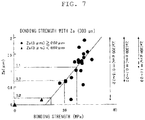
- a ceramic substrate composed of an aluminum nitride sintered compact (standard article) was used, and the same manufacturing method was carried out as in example 1, except that the conditions of the wet blasting treatment (treatment time) were changed, whereby articles were produced having varied average roughness derived in a 300- ⁇ m-wide range.
- the average roughness derived in a 3- ⁇ m-wide range was 0.02 ⁇ m or greater in all but a few cases.
- a body molded from the sealing resin 28 was formed on the surface of each of the resulting ceramic substrates, and the bonding strength was measured at room temperature in accordance with the method shown in FIG. 5 .
- the results are shown in FIG. 7 .
- black circles indicate substrates for which the average roughness derived in a 3- ⁇ m-wide range was 0.02 ⁇ m or greater, and black triangles indicate substrates for which the average roughness derived in a 3- ⁇ m-wide range was less than 0.02 ⁇ m.
- the vertical axis in FIG. 7 represents the value of the average roughness derived in a 300- ⁇ m-wide range, and the horizontal axis in FIG. 7 represents the value of the bonding strength (MPa).
- the average roughness derived in a 300- ⁇ m-wide range is preferably 0.15 to 2.0 ⁇ m, more preferably 0.7 to 2.0 ⁇ m, and most preferably 1.1 to 2.0 ⁇ m.
Landscapes
- Engineering & Computer Science (AREA)
- Chemical & Material Sciences (AREA)
- Ceramic Engineering (AREA)
- Microelectronics & Electronic Packaging (AREA)
- Manufacturing & Machinery (AREA)
- Inorganic Chemistry (AREA)
- Materials Engineering (AREA)
- Structural Engineering (AREA)
- Organic Chemistry (AREA)
- Structures Or Materials For Encapsulating Or Coating Semiconductor Devices Or Solid State Devices (AREA)
- Non-Metallic Protective Coatings For Printed Circuits (AREA)
- Cooling Or The Like Of Semiconductors Or Solid State Devices (AREA)
Abstract
Description
- The present invention relates to: a semiconductor module having a structure in which a semiconductor element is joined to an insulated substrate via a circuit pattern and in which the insulated substrate, the circuit pattern, and the semiconductor element are sealed using a sealing resin; and a method for manufacturing the semiconductor module.
- In power semiconductor modules that are used as power-conversion switching devices, e.g., as indicated in
Patent Document 1, a structure is adopted in which an insulated substrate, a circuit pattern, and a semiconductor element are sealed using a sealing resin in order to impart insulation properties, heat resistance, and durability. - However, repeated exposure to high temperature due to heat generated during operation as a switching device has resulted in delamination of an adhesive surface between the insulated substrate and the sealing resin. Delamination extending into the interior has allowed water ingress, wiring lift-off and other adverse events to occur.
- In response, technologies for increasing adhesiveness to a metal film and to a sealing resin by roughening the surface of an insulated substrate to heighten an anchoring effect have been disclosed.
- For example,
Patent Document 2 discloses a method for manufacturing a ceramic circuit substrate, the method including forming fine asperities on the surfaces of crystal particles through ion-beam etching in order to increase bonding force with a metal film. -
Patent Document 3 discloses a ceramic member in which a plurality of protrusions having a smaller diameter than the diameter of crystal particles are formed through acidic etching on the surfaces of the crystal particles in order to enhance an anchoring effect. - Patent Document 4 discloses a ceramic base body provided with a plurality of recesses and protrusions having greater asperities than the average crystal grain diameter, whereby an anchoring effect of a brazing material is enhanced.
- Furthermore, Patent Document 5 indicates that a surface is roughened by bringing abrasive grains into contact with the surface of an aluminum nitride substrate, and the joining strength of a metal circuit foil is increased.
- Furthermore, Patent Document 6 discloses an electronic control device provided with: a circuit substrate; a heat sink on which the circuit substrate is mounted; a lead electrically connected to the circuit substrate; and a sealing resin part that covers the circuit substrate as well as a connection part between the circuit substrate and the lead, the sealing resin part being such that a sealing resin is arranged so that a portion of the lead and a portion of the heat sink are exposed to the outside, wherein, in the surface of the circuit substrate and/or the surface of the heat sink, at least a portion of a site in contact with the sealing resin part is subjected to a roughening process.
-
- [Patent Document 1] Japanese Laid-open Patent Publication No.
2013-258321 - [Patent Document 2] Japanese Laid-open Patent Publication No.
H5-24959 - [Patent Document 3] Japanese Laid-open Patent Publication No.
2002-241187 - [Patent Document 4] Japanese Laid-open Patent Publication No.
2010-30280 - [Patent Document 5] Japanese Laid-open Patent Publication No.
2013-27918 - [Patent Document 6] Japanese Laid-open Patent Publication No.
2008-172172 - However, in
Patent Documents 1 to 5, no consideration is given to surface roughening of the insulated substrate for the purpose of improving bonding strength between the insulated substrate and the sealing resin. Moreover, Patent Document 6 does not specifically disclose the conditions of the roughening process. - Therefore, it cannot yet be said that the effect for improving bonding properties between an insulated substrate and a sealing resin is adequate in the features disclosed in the related art.
- Therefore, it is an object of the present invention to provide a semiconductor module in which bonding properties between an insulated substrate and a sealing resin are further improved, and a method for manufacturing the semiconductor module.
- In order to achieve the above object, a semiconductor module according to the present invention is provided with:
- an insulated substrate;
- a circuit pattern formed on the insulated substrate;
- a semiconductor element joined on the circuit pattern; and
- a sealing rein for sealing the insulated substrate, the circuit pattern, and the semiconductor element,
- the semiconductor module being characterized in that
- a surface of the insulated substrate in a portion where the insulated substrate and the sealing resin are bonded is such that, in a cross-section of the insulated substrate, the average roughness derived in a 300-µm-wide range is 0.15 µm or greater, and the average roughness derived in a 3-µm-wide range is 0.02 µm or greater, the average roughness being measured and calculated in accordance with the following method.
- A cross-section of the insulated substrate is imaged using a scanning electron microscope to prepare an SEM image, the SEM image is binarized to prepare image data for the surface shape, the image data is converted to two-dimensional coordinate data using image quantification software, and the average roughness Za is derived by computation through the following formula.

- In the formula, Za represents the average roughness. Zn represents the difference between the two-dimensional coordinate data and an average value for each n. N represents a value obtained by dividing a measured width by a measured pitch; in computation of the roughness for a width of 300 µm, the pitch is equal to 0.5 µm, that means N is equal to 600, and in computation of the roughness for a width of 3 µm, the pitch is equal to 0.005 µm, that means N is equal to 600.
- In the semiconductor module according to the present invention, the portion where the insulated substrate and the sealing resin are bonded preferably includes a peripheral edge part of the insulated substrate.
- The surface of the insulated substrate in the portion where the insulated substrate and the sealing resin are bonded preferably is such that, in a cross-section of the insulated substrate, the average roughness derived in a 300-µm-wide range is 2 µm or less.
- The surface of the insulated substrate in the portion where the insulated substrate and the sealing resin are bonded furthermore preferably is such that, in a cross-section of the insulated substrate, the average roughness derived in a 300-µm-wide range is 0.7 µm or greater.
- The surface of the insulated substrate in the portion where the insulated substrate and the sealing resin are bonded yet furthermore preferably is such that the average roughness derived in a 3-µm-wide range is 0.1 µm or less.
- In addition, a method for manufacturing a semiconductor module according to the present invention is provided with:
- a surface treatment step for adjusting the surface roughness of a ceramic insulated substrate;
- an oxidizing treatment step for heat-treating the insulated substrate to oxidize the surface of the insulated substrate;
- a brazing material application step for applying a brazing material to the surface of the insulated substrate;
- a metal foil joining step for joining a metal foil to the surface of the insulated substrate via the brazing material;
- a circuit pattern formation step for etching the metal foil and the brazing material to form a circuit pattern;
- a semiconductor element implementation step for joining a semiconductor element to the circuit pattern; and
- a sealing step for sealing the insulated substrate, the circuit pattern, and the semiconductor element using a sealing resin,
- the method for manufacturing a semiconductor module being characterized in that:
- the surface treatment step includes a step for performing a wet blasting treatment on the surface of the insulated substrate to roughen the surface so as to reach an average roughness of 0.15 µm or greater as derived in a 300-µm-wide range in a cross-section of the insulated substrate;
- the brazing material application step included a step for applying the brazing material not only to the surface of the insulated substrate where the metal foil is joined, but also to a surface of the insulated substrate where the metal foil is not joined, the surface being where the sealing resin is bonded; and
- in the circuit pattern formation step, a portion where the brazing material is applied is etched, whereby the surface of the insulated substrate where the sealing resin is bonded is configured to have a surface roughness such that, in a cross-section of the insulated substrate, the average roughness derived in a 300-µm-wide range is 0.15 µm or greater, and the average roughness derived in a 3-µm-wide range is 0.02 µm or greater, the average roughness being measured and calculated in accordance with the method described above.
- In the method for manufacturing a semiconductor according to the present invention, the insulated substrate is preferably made of a ceramic, and is more preferably composed of aluminum nitride.
- In addition, an insulated circuit substrate according to the present invention is provided with:
- an insulated substrate; and
- a circuit pattern formed on the insulated substrate,
- the insulated circuit substrate being characterized in that
- a surface of the insulated substrate in a portion where the circuit pattern is not formed is such that, in a cross-section of the insulated substrate, the average roughness derived in a 300-µm-wide range is 0.15 µm or greater, and the average roughness derived in a 3-µm-wide range is 0.02 µm or greater, the average roughness being measured and calculated in accordance with the method described above.
- In the semiconductor module according to the present invention, the surface of the insulated substrate in the portion where the insulated substrate and the sealing resin are bonded is such that, in a cross-section of the insulated substrate, the average roughness derived in a 300-µm-wide range is 0.15 µm or greater, and the average roughness derived in a 3-µm-wide range is 0.02 µm or greater. This improves the bonding strength between the insulated substrate and the sealing resin, maintains a high bonding strength even under high temperature, and suppresses delamination of the sealing resin. It is therefore possible to improve the durability of the semiconductor module.
- In the method for manufacturing a semiconductor module according to the present invention, comparatively rough asperities are formed in the surface of the insulated substrate through the wet blasting treatment, and the brazing material is furthermore applied and etched in the surface to which the metal foil is not joined, the surface being where the sealing resin is directly bonded. This makes it possible to furthermore form fine asperities in the surface having the comparatively rough asperities, further increases the bonding strength of the sealing resin by the rough surface in which the fine asperities are furthermore formed in the surface having the rough asperities, and makes it possible to suppress delamination of the sealing resin.
- In the insulated circuit substrate according to the present invention, when it is used as an insulated circuit substrate of a semiconductor module and is sealed using a sealing resin, the bonding strength between the insulated substrate and the sealing resin increases, a high bonding strength is maintained even under high temperature, and delamination of the sealing resin is suppressed. It is therefore possible to improve the durability of the semiconductor module.
-
-
FIG. 1 is a cross-sectional view of a semiconductor module according to an embodiment of the present invention; -
FIG. 2 is a cross-sectional view of a semiconductor module according to another embodiment of the present invention; -
FIG. 3 is a schematic diagram showing the roughness of the surface of an insulated substrate in the semiconductor module according to the present invention; -
FIG. 4 is an explanatory drawing showing a computational formula for surface roughness and a general concept underlying the same; -
FIG. 5 is an explanatory drawing showing a method for measuring the delamination strength between the insulated substrate and a sealing resin; -
FIG. 6 is a graph showing the results of measuring the delamination strength between the insulated substrate and the sealing resin; and -
FIG. 7 is another graph showing the results of measuring the delamination strength between the insulated substrate and the sealing resin. - Embodiments of a semiconductor module according to the present invention are described below with reference to the accompanying drawings.
-
FIG. 1 shows a first embodiment of a semiconductor module to which the present invention is applied. Thesemiconductor module 50 is a power semiconductor module, wherein acircuit pattern 24 is formed on the upper surface of aninsulated substrate 23, and ametal sheet 22 having excellent thermal conductivity is joined to the lower surface of theinsulated substrate 23. Aninsulated circuit substrate 21 is configured from the insulatedsubstrate 23, thecircuit pattern 24, and themetal sheet 22. - A ceramic substrate in which the main component is, e.g., aluminum nitride, alumina, or silicon nitride is preferably used as the
insulated substrate 23. However, it is also possible to use, inter alia, a substrate in which the surface of a metal sheet composed of aluminum, etc., is coated with an insulating resin layer. A ceramic substrate composed of an aluminum nitride sintered compact is particularly preferred. The average crystal grain diameter of the ceramic in the ceramic substrate is preferably 0.5 to 20 µm, and more preferably 2 to 7 µm. The aluminum nitride sintered compact can be obtained by sintering a molded body composed of an aluminum nitride raw powder having an average particle diameter of 0.1 to 15 µm. The molded body may include a sintering auxiliary agent, an organic binder, etc., as necessary. - An article obtained by etching a metal foil joined to the
insulated substrate 23 via a brazing material to form a pattern is preferably employed as thecircuit pattern 24. The metal foil is not particularly limited; however, as an example, copper is preferably employed. Themetal sheet 22 is not particularly limited, provided that themetal sheet 22 has excellent thermal conductivity; however, as an example, a metal sheet made of copper, aluminum, a copper alloy, or an aluminum alloy is used. -
Semiconductor elements circuit pattern 24 viasolder 29. Anexternal terminal 12 is provided upright on thecircuit pattern 24 via thesolder 29, and thesemiconductor elements external terminal 12 are connected by thecircuit pattern 24 or abonding wire 27. - The
semiconductor elements - Furthermore, the
insulated substrate 23, thecircuit pattern 24, thesemiconductor elements external terminal 12, and the side surfaces of themetal sheet 22 are sealed using a sealingresin 28, with the lower surface of themetal sheet 22 and the upper portion of theexternal terminal 12 being excluded from sealing. The sealingresin 28 is not particularly limited; however, as an example, an epoxy resin, a maleimide resin, a silicone resin, or a liquid crystal polymer is used. - The sealing
resin 28 is bonded to each of theinsulated substrate 23, thecircuit pattern 24, thesemiconductor elements external terminal 12, and the side surfaces of themetal sheet 22. Theinsulated substrate 23 has asurface 23a that is bonded (adherent) to the sealing resin 28 (referred to as a "sealing-resin-bonded surface" below). The sealing-resin-bondedsurface 23a is formed as being a peripheral edge part of theinsulated substrate 23 so as to surround the outer periphery of themetal sheet 22 and thecircuit pattern 24. In the present embodiment, the sealing-resin-bondedsurface 23a is formed, in addition to as being the peripheral edge part on the upper-surface side of theinsulated substrate 23, it is formed as being the outer-peripheral-side surface of theinsulated substrate 23 and as being the peripheral edge part on the lower-surface side of theinsulated substrate 23, the peripheral edge part being positioned on the outer periphery of themetal sheet 22. -
FIG. 2 shows another embodiment of a semiconductor module to which the present invention is applied. Thissemiconductor module 50a also is a power semiconductor module, wherein acircuit pattern 24 is formed on the upper surface of aninsulated substrate 23, and ametal sheet 22 having excellent thermal conductivity is joined to the lower surface of theinsulated substrate 23. Aninsulated circuit substrate 21 is configured from the insulatedsubstrate 23, thecircuit pattern 24, and themetal sheet 22. - However, in this
semiconductor module 50a, a frame-shapedcase 13 made of a resin is provided surrounding theinsulated circuit substrate 21, and the peripheral edge part of the insulatedcircuit substrate 21 is anchored to thecase 13 via an adhesive 14. A lower portion of anexternal terminal 12 that is bent in an L-shape is integrally molded with thecase 13 so as to be exposed to the interior of thecase 13 through thecase 13, constituting aninsert case 11. -
Semiconductor elements circuit pattern 24 viasolder 29. Thesemiconductor elements external terminal 12 are connected by thecircuit pattern 24 or abonding wire 27. - Furthermore, the interior of the
case 13 is filled with a sealingresin 28, and theinsulated substrate 23, thecircuit pattern 24, thesemiconductor elements external terminal 12 are sealed by the sealingresin 28. In the present embodiment as well, theinsulated substrate 23 has a sealing-resin-bondedsurface 23a that is bonded (adherent) to the sealingresin 28. The sealing-resin-bondedsurface 23a is formed as being the peripheral edge part of theinsulated substrate 23. - The characteristics of the semiconductor module according to the present invention are such that the surface roughness on the sealing-resin-bonded
surface 23a of theinsulated substrate 23 in thesemiconductor module - Specifically, the
semiconductor module surface 23a of theinsulated substrate 23. A method for measuring and calculating the average roughness employed in the present invention is described in detail below. -
FIG. 3 depicts the surface shape in a cross-section of theinsulated substrate 23 at the sealing-resin-bondedsurface 23a. The surface shape from the cross-section of theinsulated substrate 23 can be extracted by imaging a cross-section perpendicular to the surface of the substrate using a scanning electron microscope to prepare an SEM image, binarizing the SEM image to prepare image data that reflects the surface shape, and converting the image data to two-dimensional coordinate data. - The SEM image can be binarized by maximizing the contrast using software that has an image processing function, such as "Microsoft PowerPoint" (trade name; produced by Microsoft Corp.). Other software may also be used as the software that has an image processing function.
-
FIG. 3(A) shows a shape taken along the surface of a cross-section of theinsulated substrate 23 so that the width indicated by arrows in the drawing is 300 µm.FIG. 3(B) shows a shape in which a portion of the aforementioned shape is taken so that the width indicated by arrows in the drawing is 3 µm.Reference symbol 30 indicates the surfaces of crystal grains. - The surface shape in
FIG. 3(A) (width: 300 µm) can be retrieved using, e.g., an SEM image captured at a magnification of 1,000×. The surface shape inFIG. 3(B) (width: 3 µm) can be retrieved using, e.g., an SEM image of the surfaces of crystal grains captured at a magnification of 15,000×. - Such a binarized image of the surface shape can be quantified using image quantification software, such as "Graphcel" (trade name; freeware), and then the average roughness can be derived through calculation by the following numerical formula shown in
FIG. 4 using spreadsheet software, such as "Microsoft Excel" (trade name; produced by Microsoft Corp.) .
- In the above numerical formula, Za represents the average roughness. Zn represents the difference between the two-dimensional coordinate data and an average value for each n. N represents a value obtained by dividing a measured width by a measured pitch; in computation of the roughness for a width of 300 µm, the pitch is equal to 0.5 µm, that means N is equal to 600, and in computation of the roughness for a width of 3 µm, the pitch is equal to 0.005 µm, that means N is equal to 600.
- To measure the average roughness, the surface shape from the cross-section is measured in three or more locations, and the average value thereof is used as a measurement value.
- In the present invention, when, e.g., the width of 300 µm shown by the arrows in
FIG. 3(A) is used as a reference length L, a value in which the average roughness is derived through the formula shown inFIG. 4 from the surface shape of that portion is 0.15 µm or greater. Moreover, when the width of 3 µm shown by the arrows inFIG. 3(B) is used as the reference length L, a value in which the average roughness is derived through the formula shown inFIG. 4 from the surface shape of that portion is 0.02 µm or greater. - Forming the sealing-resin-adhering
surface 23a of theinsulated substrate 23 so as to yield the surface shape described above improves the bonding strength between theinsulated substrate 23 and the sealingresin 28, maintains a high bonding strength even under high temperature, and suppresses delamination of the sealing resin. It is therefore possible to improve the durability of the semiconductor module. In addition, the sealing-resin-adheringsurface 23a of theinsulated substrate 23 is formed as being the peripheral edge of theinsulated substrate 23 so as to surround thecircuit pattern 24, and delamination at that portion is suppressed, thereby making it possible to more solidly protect thecircuit pattern 24 and thesemiconductor elements - The average roughness of the sealing-resin-adhering
surface 23a of theinsulated substrate 23 as derived in a 300-µm-wide range is preferably 0.7 µm or greater, and more preferably 1.1 µm or greater, in order to further increase the bonding strength between theinsulated substrate 23 and the sealingresin 28. However, the average roughness derived in the range having a width of 300 µm is preferably no greater than 2 µm so as not to adversely affect the shape of thecircuit pattern 24, etc. - The average roughness of the sealing-resin-adhering
surface 23a of theinsulated substrate 23 as derived in a 3-µm-wide range is preferably 0.1 µm or less, in order to increase the bonding strength between theinsulated substrate 23 and the sealingresin 28. - A method for manufacturing a semiconductor module according to the present invention is described next.
- In the method for manufacturing a semiconductor module according to the present invention, a ceramic substrate is used as the
insulated substrate 23. In particular, it is preferable to use a ceramic substrate composed of an aluminum nitride sintered compact. - The surface of the
insulated substrate 23 is subjected to a wet blasting treatment and is roughened so that, in a cross-section of theinsulated substrate 23, the average roughness derived in a 300-µm-wide range is 0.15 µm or greater. - The wet blasting treatment can be performed by using abrasive grains that have a higher hardness than the ceramic substrate, forming a liquid that includes the abrasive grains, and jetting the liquid onto the ceramic substrate together with compressed air. In such instances, the value of the average roughness derived in a 300-µm-wide range can be adjusted by adjusting the particle size of the abrasive grains or the jetting pressure.
- The
insulated substrate 23 is then heat-treated to oxidize the surface of theinsulated substrate 23. The heat treatment can be performed by, e.g., holding the temperature at 800 to 1200°C, and preferably 1000 to 1100°C, for 2 to 12 hours. - A brazing material is then applied to the surface of the
insulated substrate 23. It is preferable to use, as the brazing material, e.g., an active metal brazing material in which at least one active metal selected from Ti, Zr, Hf, Nb, etc., is included in an Ag-Cu brazing material. Sn, In, etc., may also be included as necessary. The active metal brazing material can preferably be used in the form of a paste. The brazing material can be applied, e.g., by screen printing, using a roll coater, or employing other techniques. - Conventionally, it is common for brazing materials to be applied only to a portion of the surface of the
insulated substrate 23 where the metal foil for forming thecircuit pattern 24 was to be joined. However, in the present invention, the brazing material is also applied to a portion where the metal foil is not joined, the portion forming a portion of the sealing-resin-adheringsurface 23a of theinsulated substrate 23. The brazing material is preferably applied to the entirety of the sealing-resin-adheringsurface 23a of theinsulated substrate 23. - The metal foil for forming the
circuit pattern 24 is then disposed at a prescribed location in the portion of the surface of theinsulated substrate 23 where the brazing material is applied, pressure is applied as necessary in this state, and heat treatment is conducted, whereby the brazing material is melted and the metal foil is joined to the surface of theinsulated substrate 23 via the brazing material. - After the metal foil is joined in this manner, the metal foil and the brazing material are patterned by etching using a well-known method such as photo-etching to form the
circuit pattern 24. - In such instances, the surface of the
insulated substrate 23, which is appeared by etching and removing the brazing material anchored to the surface of theinsulated substrate 23, is treated so that fine asperities having an average roughness of 0.02 µm or greater as derived in a 3-µm-wide range are formed in a surface having comparatively large asperities, the surface being formed, during the surface treatment step, by roughening so as to have an average roughness of 0.15 µm or greater as derived in a 300-µm-wide range. - The fine asperities are formed by etching and removing the brazing material anchored to the surface of the
insulated substrate 23; such asperities would not be formed by etching a surface of theinsulated substrate 23 that had been subjected merely to the oxidizing treatment. Therefore, the present invention is configured so that, in the brazing material application step, the brazing material is also applied to the portion where the metal foil is not joined in the portion of theinsulated substrate 23 that forms the sealing-resin-adheringsurface 23a. - After the
circuit pattern 24 is formed in this manner, thesemiconductor elements external terminal 12 are joined viasolder 29 in accordance with a usual method. - Finally, inter alia, the
insulated substrate 23, thecircuit pattern 24, thesemiconductor elements external terminal 12 are sealed by the sealingresin 28, whereby thesemiconductor module - In the resulting
semiconductor module surface 23a of theinsulated substrate 23 has comparatively rough asperities such that the average roughness derived in a 300-µm-wide range is 0.15 µm or greater, the surface shape being one in which fine asperities such that the average roughness derived in a 3-µm-wide range is 0.02 µm or greater are formed in the surface having comparatively large asperities. Therefore, as described above, the bonding strength between theinsulated substrate 23 and the sealingresin 28 is improved, a high bonding strength is maintained even under high temperature, and delamination of the sealing resin is suppressed. It is therefore possible to improve the durability of the semiconductor module. - A ceramic substrate composed of an aluminum nitride sintered compact was used as the insulated substrate, an epoxy resin was used as the sealing resin, the surface roughness of the insulated substrate was changed, and the bonding strength between the insulated substrate and the sealing resin was measured.
- A mold (not shown) was placed on the
insulated substrate 23, resin was charged into the mold through holes provided therein, and the resin was thermally cured at 170°C for 60 minutes, whereby sealingresin 28 having the size and shape shown inFIG. 5 (frustoconical, measuring 3.57 mm in bottom-surface diameter, 3 mm in upper-surface diameter, and 4 mm in height) was molded while joined to theinsulated substrate 23, as shown inFIG. 5 . - This sample was placed on a shear testing device (testing device in which a "DIGITAL FORCE GAUGE Model ZP-1000N" manufactured by Imada Co., Ltd., and a "FORCE GAUGE STAND Model FGS-50D" manufactured by Shimpo Industrial Co., Ltd., were combined), a
plunger 40 was pressed against the molded sealingresin 28, the maximum load (kgf) when pressing and breaking at a shear velocity of 0.03 mm/sec was measured, and a bonding strength (MPa) was derived by dividing the resulting load by 10 mm2. - A body molded from the sealing
resin 28 was formed through the method described above on the surface of a ceramic substrate composed of an aluminum nitride sintered compact (referred to as a "standard article" below), the ceramic substrate having a surface roughness such that the average roughness derived in a 300-µm-wide range was 0.10 µm, and the average roughness derived in a 3-µm-wide range was 0.015 µm. - An active-metal-containing paste brazing material (in which the weight ratio of metal components, i.e., Ag:Cu:Ti is equal to 80:17:3) was applied to the standard-article ceramic substrate, a copper foil made of oxygen-free copper was laminated on the brazing material, and the brazing material was melted by heating in a vacuum at 850°C and then solidified, whereby the copper foil was anchored via the brazing material to the surface of the ceramic substrate. The metal foil was then removed using a cupric chloride etching liquid. The ceramic substrate was then immersed at 20°C for 15 minutes in an aqueous solution including 5% hydrogen peroxide, 3% ammonia, and 1.6% by weight of EDTA, and then rinsed. The ceramic substrate was then immersed at 30°C for 30 minutes in an aqueous solution including 2% DTPA-5Na and 5% hydrogen peroxide, whereby the brazing material was removed. A ceramic substrate was thus formed having a surface roughness such that the average roughness derived in a 300-µm-wide range was 0.10 µm, and the average roughness derived in a 3-µm-wide range was 0.025 µm. A body molded from the sealing
resin 28 was formed on the surface of the substrate using the method described above. - The surface of the standard-article ceramic substrate was treated using a wet blast machine manufactured by Fuji Kiko Co., Ltd., using a no. 320 alumina abrasive material at a pressure of 0.2 MPa. The ceramic substrate was then heat-treated in atmospheric air at 1050°C for 2 hours to oxidize the surface thereof, and a ceramic substrate was formed having a surface roughness such that the average roughness derived in a 300-µm-wide range was 0.33 µm, and the average roughness derived in a 3-µm-wide range was 0.015 µm. A body molded from the sealing
resin 28 was formed on the surface of the substrate using the method described above. - The surface of the standard-article ceramic substrate was subjected to wet-blasting and oxidizing treatments under the same conditions as in comparative example 3, and a ceramic substrate was formed having a surface roughness such that the average roughness derived in a 300-µm-wide range was 0.33 µm, and the average roughness derived in a 3-µm-wide range was 0.015 µm. A brazing material was then applied under the same conditions as in comparative example 2, a copper foil was laminated thereon, and the brazing material was melted by heating in a vacuum at 850°C and then solidified, whereby the copper foil was anchored via the brazing material to the surface of the ceramic substrate. The ceramic substrate was then immersed in an etching liquid in the same manner as in comparative example 2, and the copper foil, the brazing material, and a reaction layer were removed. A ceramic substrate was thus formed having a surface roughness such that the average roughness derived in a 300-µm-wide range was 0.33 µm, and the average roughness derived in a 3-µm-wide range was 0.025 µm. A body molded from the sealing
resin 28 was formed on the surface of the substrate using the method described above. - The bonding strength (MPa) of the resulting samples in comparative examples 1 to 3 and example 1 was measured in accordance with the method shown in
FIG. 5 . The bonding strength was measured at both room temperature (R.T.; 25°C) and a high temperature of 150°C. The results are shown inFIG. 6 . - As shown in
FIG. 6 , the bonding strength was very low in comparative example 1, in which the standard article of a ceramic substrate composed of an aluminum nitride sintered compact was used without modification. - In the evaluation of bonding strength in comparative example 2, in which a molded article of the sealing
resin 28 was formed on the surface of a ceramic substrate subjected to the processes in comparative example 2, the bonding strength was nearly doubled at both room temperature and high temperature, but still could not be said to be sufficient strength. - In the evaluation of bonding strength in comparative example 3, in which a molded article of the sealing
resin 28 was formed on the surface of a ceramic substrate subjected to the processes in comparative example 3, the bonding strength improved at both room temperature and high temperature, but did not reach 25 MPa, which is a target value from the standpoint of adequately imparting heat resistance and durability to a semiconductor module. - However, in the evaluation of bonding strength in example 1, in which a molded article of the sealing
resin 28 was formed on the surface of a ceramic substrate subjected to the processes in example 1, the bonding strength was notably improved at both room temperature and high temperature, and it was possible to reach a bonding strength of 25 MPa, which is the target value from the standpoint of adequately imparting heat resistance and durability to a semiconductor module. - Thus, it is understood that it is possible to rapidly increase the bonding strength between an insulated substrate and a sealing resin by forming comparatively large asperities through a wet blasting treatment, subsequently performing an oxidizing treatment, and furthermore forming comparatively fine asperities through an etching treatment to achieve an average roughness of 0.15 µm or greater as derived in a 300-µm-wide range and moreover an average roughness of 0.02 µm or greater as derived in a 3-µm-wide range.
- A ceramic substrate composed of an aluminum nitride sintered compact (standard article) was used, and the same manufacturing method was carried out as in example 1, except that the conditions of the wet blasting treatment (treatment time) were changed, whereby articles were produced having varied average roughness derived in a 300-µm-wide range. The average roughness derived in a 3-µm-wide range was 0.02 µm or greater in all but a few cases.
- A body molded from the sealing
resin 28 was formed on the surface of each of the resulting ceramic substrates, and the bonding strength was measured at room temperature in accordance with the method shown inFIG. 5 . The results are shown inFIG. 7 . InFIG. 7 , black circles indicate substrates for which the average roughness derived in a 3-µm-wide range was 0.02 µm or greater, and black triangles indicate substrates for which the average roughness derived in a 3-µm-wide range was less than 0.02 µm. The vertical axis inFIG. 7 represents the value of the average roughness derived in a 300-µm-wide range, and the horizontal axis inFIG. 7 represents the value of the bonding strength (MPa). - As shown in
FIG. 7 , there was a tendency for the bonding strength to increase commensurately with an increase in the average roughness derived in a 300-µm-wide range. However, as the average roughness derived in a 300-µm-wide range approached 2 µm, the bonding strength tended not to improve any further. - Therefore, the average roughness derived in a 300-µm-wide range is preferably 0.15 to 2.0 µm, more preferably 0.7 to 2.0 µm, and most preferably 1.1 to 2.0 µm.
-
- 11
- Insert case
- 12
- External terminal
- 13
- Case
- 14
- Adhesive
- 21
- Insulated circuit substrate
- 22
- Metal sheet
- 23
- Insulated substrate
- 24
- Circuit pattern
- 25, 26
- Semiconductor element
- 27
- Bonding wire
- 28
- Sealing resin
- 29
- Solder
- 30
- Surfaces of crystal grains
- 50, 50a
- Semiconductor module
Claims (10)
- A semiconductor module comprising:an insulated substrate;a circuit pattern formed on the insulated substrate;a semiconductor element joined on the circuit pattern; anda sealing resin for sealing the insulated substrate, the circuit pattern, and the semiconductor element,the semiconductor module being characterized in thata surface of the insulated substrate in a portion where the insulated substrate and the sealing resin are bonded is such that, in a cross-section of the insulated substrate, the average roughness derived in a 300-µm-wide range is 0.15 µm or greater, and the average roughness derived in a 3-µm-wide range is 0.02 µm or greater, the average roughness being measured and calculated in accordance with the following method.(Method for measuring/calculating average roughness)A cross-section of the insulated substrate is imaged using a scanning electron microscope to prepare an SEM image, the SEM image is binarized to prepare image data for the surface shape, the image data is converted to two-dimensional coordinate data using image quantification software, and the average roughness Za is derived by computation through the following formula.

- The semiconductor module according to claim 1, wherein the portion where the insulated substrate and the sealing resin are bonded includes a peripheral edge part of the insulated substrate.
- The semiconductor module according to claim 1 or 2, wherein the surface of the insulated substrate in the portion where the insulated substrate and the sealing resin are bonded is such that, in the cross-section of the insulated substrate, the average roughness derived in a 300-µm-wide range is 2 µm or less.
- The semiconductor module according to any of claims 1 to 3, wherein the surface of the insulated substrate in the portion where the insulated substrate and the sealing resin are bonded is such that, in the cross-section of the insulated substrate, the average roughness derived in a 300-µm-wide range is 0.7 µm or greater.
- The semiconductor module according to any of claims 1 to 4, wherein the surface of the insulated substrate in the portion where the insulated substrate and the sealing resin are bonded is such that the average roughness derived in a 3-µm-wide range is 0.1 µm or less.
- A method for manufacturing a semiconductor module, the method including:a surface treatment step for adjusting the surface roughness of a ceramic insulated substrate;an oxidizing treatment step for heat-treating the insulated substrate to oxidize the surface of the insulated substrate;a brazing material application step for applying a brazing material to the surface of the insulated substrate;a metal foil joining step for joining a metal foil to the surface of the insulated substrate via the brazing material;a circuit pattern formation step for etching the metal foil and the brazing material to form a circuit pattern;a semiconductor element implementation step for joining a semiconductor element to the circuit pattern; anda sealing step for sealing the insulated substrate, the circuit pattern, and the semiconductor element using a sealing resin,the method for manufacturing a semiconductor module being characterized in that:the surface treatment step includes a step for performing a wet blasting treatment on the surface of the insulated substrate to roughen the surface;the brazing material application step includes a step for applying the brazing material not only to the surface of the insulated substrate where the metal foil is joined, but also to a surface of the insulated substrate where the metal foil is not joined, said surface being where the sealing resin is bonded; andin the circuit pattern formation step, a portion where the brazing material is applied is etched, whereby the surface of the insulated substrate where the sealing resin is bonded is configured to have a surface roughness such that, in a cross-section of the insulated substrate, the average roughness derived in a 300-µm-wide range is 0.15 µm or greater, and the average roughness derived in a 3-µm-wide range is 0.02 µm or greater, the average roughness being measured and calculated in accordance with the following method.(Method for measuring/calculating average roughness)A cross-section of the insulated substrate is imaged using a scanning electron microscope to prepare an SEM image, the SEM image is binarized to prepare image data for the surface shape, the image data is converted to two-dimensional coordinate data using image quantification software, and the average roughness Za is derived by computation through the following formula.

- The method for manufacturing a semiconductor module according to claim 6, wherein the insulated substrate is composed of aluminum nitride.
- The semiconductor module according to any of claims 1 to 5, wherein the insulated substrate is made of ceramic.
- The semiconductor module according to claim 8, wherein the insulated substrate is composed of aluminum nitride.
- An insulated circuit substrate having:an insulated substrate; anda circuit pattern formed on the insulated substrate,the insulated circuit substrate being characterized in thata surface of the insulated substrate in a portion where the circuit pattern is not formed is such that, in a cross-section of the insulated substrate, the average roughness derived in a 300-µm-wide range is 0.15 µm or greater, and the average roughness derived in a 3-µm-wide range is 0.02 µm or greater, the average roughness being measured and calculated in accordance with the following method.(Method for measuring/calculating average roughness)A cross-section of the insulated substrate is imaged using a scanning electron microscope to prepare an SEM image, the SEM image is binarized to prepare image data for the surface shape, the image data is converted to two-dimensional coordinate data using image quantification software, and the average roughness Za is derived by computation through the following formula

Applications Claiming Priority (2)
| Application Number | Priority Date | Filing Date | Title |
|---|---|---|---|
| JP2018027138A JP7083256B2 (en) | 2018-02-19 | 2018-02-19 | Semiconductor module and its manufacturing method |
| PCT/JP2019/004302 WO2019159798A1 (en) | 2018-02-19 | 2019-02-06 | Semiconductor module and method for manufacturing same |
Publications (2)
| Publication Number | Publication Date |
|---|---|
| EP3712933A1 true EP3712933A1 (en) | 2020-09-23 |
| EP3712933A4 EP3712933A4 (en) | 2020-12-30 |
Family
ID=67619347
Family Applications (1)
| Application Number | Title | Priority Date | Filing Date |
|---|---|---|---|
| EP19753674.1A Pending EP3712933A4 (en) | 2018-02-19 | 2019-02-06 | SEMICONDUCTOR MODULE AND METHOD OF MANUFACTURING THEREOF |
Country Status (6)
| Country | Link |
|---|---|
| US (1) | US11749581B2 (en) |
| EP (1) | EP3712933A4 (en) |
| JP (1) | JP7083256B2 (en) |
| KR (1) | KR102454589B1 (en) |
| CN (1) | CN111512434B (en) |
| WO (1) | WO2019159798A1 (en) |
Cited By (2)
| Publication number | Priority date | Publication date | Assignee | Title |
|---|---|---|---|---|
| EP4015486A4 (en) * | 2019-08-16 | 2022-09-28 | Denka Company Limited | CERAMIC SUBSTRATE, PRINTED CIRCUIT BOARD AND METHOD FOR PRODUCTION THEREOF, AND POWER MODULE |
| US12412847B2 (en) * | 2022-03-14 | 2025-09-09 | Fuji Electric Co., Ltd. | Semiconductor module, semiconductor device and vehicle |
Families Citing this family (7)
| Publication number | Priority date | Publication date | Assignee | Title |
|---|---|---|---|---|
| US20200315023A1 (en) * | 2019-03-25 | 2020-10-01 | Intel Corporation | Copper interface features for high speed interconnect applications |
| JP7494521B2 (en) * | 2020-03-30 | 2024-06-04 | 富士電機株式会社 | Semiconductor device and method for manufacturing the same |
| DE112021006959T5 (en) | 2021-01-28 | 2023-11-16 | Ngk Insulators, Ltd. | Separating membrane complex and process for producing a separating membrane complex |
| CN112979322B (en) * | 2021-02-20 | 2023-09-08 | 北京北方华创微电子装备有限公司 | Ceramic part and manufacturing method thereof |
| CN118215995A (en) * | 2021-11-10 | 2024-06-18 | 株式会社村田制作所 | Modules |
| DE102023126070A1 (en) * | 2023-09-26 | 2025-03-27 | Rogers Germany Gmbh | Method for producing a metal-ceramic substrate and metal-ceramic substrate |
| CN120048803A (en) * | 2023-11-24 | 2025-05-27 | 华为数字能源技术有限公司 | Power module, manufacturing method and electronic equipment |
Family Cites Families (30)
| Publication number | Priority date | Publication date | Assignee | Title |
|---|---|---|---|---|
| JP3176089B2 (en) | 1991-07-25 | 2001-06-11 | 松下電工株式会社 | Manufacturing method of ceramic circuit board |
| JP3350269B2 (en) * | 1995-02-09 | 2002-11-25 | 京セラ株式会社 | Semiconductor device |
| KR100855529B1 (en) * | 1998-09-03 | 2008-09-01 | 이비덴 가부시키가이샤 | Multilayer printed wiring board and method for manufacturing the same |
| KR100712715B1 (en) | 2001-01-31 | 2007-05-04 | 도시바세라믹스가부시키가이샤 | Ceramics member of which fine projections are formed in the surface and method for producing it |
| JP3865588B2 (en) | 2001-02-09 | 2007-01-10 | 東芝セラミックス株式会社 | Ceramic member having fine protrusions formed on its surface, and method for producing the same |
| TWI255001B (en) | 2001-12-13 | 2006-05-11 | Matsushita Electric Industrial Co Ltd | Metal wiring substrate, semiconductor device and the manufacturing method thereof |
| KR100618630B1 (en) * | 2003-10-24 | 2006-09-13 | 도시바세라믹스가부시키가이샤 | Plasma resistant member, manufacturing method for the same and method of forming a thermal spray coat |
| JP2005225745A (en) | 2004-01-16 | 2005-08-25 | Toshiba Ceramics Co Ltd | Plasma-resistant member and manufacturing method thereof |
| US8569142B2 (en) * | 2003-11-28 | 2013-10-29 | Blackberry Limited | Multi-level thin film capacitor on a ceramic substrate and method of manufacturing the same |
| EP1588803A1 (en) | 2004-04-21 | 2005-10-26 | JSR Corporation | Chemical mechanical polishing pad, manufacturing process thereof and chemical mechanical polishing method |
| JP2006145320A (en) * | 2004-11-18 | 2006-06-08 | Matsushita Electric Works Ltd | Semiconductor device and its manufacturing method |
| JP2008172172A (en) | 2007-01-15 | 2008-07-24 | Denso Corp | Electronic control device and manufacturing method thereof |
| JP5181618B2 (en) | 2007-10-24 | 2013-04-10 | 宇部興産株式会社 | Metal foil laminated polyimide resin substrate |
| EP2315508B1 (en) * | 2008-06-20 | 2014-11-12 | Hitachi Metals, Ltd. | Collective ceramic substrate, manufacturing method for the substrate, ceramic substrate, and ceramic circuit substrate |
| JP5473407B2 (en) | 2008-06-27 | 2014-04-16 | 京セラ株式会社 | Ceramic substrate, heat dissipation substrate, and electronic device |
| WO2010013470A1 (en) | 2008-07-31 | 2010-02-04 | 三洋電機株式会社 | Semiconductor module and portable apparatus provided with semiconductor module |
| JP5484705B2 (en) | 2008-09-30 | 2014-05-07 | 三洋電機株式会社 | Semiconductor module and portable device equipped with semiconductor module |
| JP2010087229A (en) * | 2008-09-30 | 2010-04-15 | Sanyo Electric Co Ltd | Semiconductor module, method of manufacturing semiconductor module, and portable device |
| EP2405725A1 (en) * | 2009-02-12 | 2012-01-11 | Sumitomo Bakelite Company Limited | Resin composition for wiring board, resin sheet for wiring board, composite body, method for producing composite body, and semiconductor device |
| JP2011052240A (en) | 2009-08-31 | 2011-03-17 | Denso Corp | Method for manufacturing structure provided with thermal-sprayed insulation film |
| JP2012054368A (en) | 2010-08-31 | 2012-03-15 | Fujifilm Corp | Method of manufacturing multilayer wiring board |
| KR20120050755A (en) * | 2010-11-11 | 2012-05-21 | 삼성전기주식회사 | Semiconductor package substrate and method for manufacturing the same |
| JP5911231B2 (en) | 2011-07-29 | 2016-04-27 | 株式会社トクヤマ | Method for manufacturing aluminum nitride-metal bonded substrate |
| JP5896214B2 (en) * | 2012-01-23 | 2016-03-30 | 日亜化学工業株式会社 | Manufacturing method of semiconductor device |
| JP2013258321A (en) * | 2012-06-13 | 2013-12-26 | Fuji Electric Co Ltd | Semiconductor device |
| EP3026145A4 (en) * | 2013-07-23 | 2017-04-12 | JX Nippon Mining & Metals Corporation | Treated surface copper foil, copper foil with carrier, substrate, resin substrate, printed circuit board, copper clad laminate, and printed circuit board manufacturing method |
| JP5799154B2 (en) | 2013-12-13 | 2015-10-21 | Jx日鉱日石金属株式会社 | Sputtering target and manufacturing method thereof |
| JP2017011049A (en) * | 2015-06-19 | 2017-01-12 | 株式会社日立製作所 | Insulation circuit board, and power semiconductor device using the same |
| CN107563087B (en) * | 2017-09-13 | 2020-12-15 | 绍兴文理学院 | A Statistical Method of Surface Roughness Coefficient under Optimal Sampling Spacing |
| US10510686B2 (en) * | 2018-04-27 | 2019-12-17 | Taiwan Semiconductor Manufacturing Co., Ltd. | Semiconductor package and manufacturing method thereof |
-
2018
- 2018-02-19 JP JP2018027138A patent/JP7083256B2/en active Active
-
2019
- 2019-02-06 KR KR1020207017893A patent/KR102454589B1/en active Active
- 2019-02-06 US US16/955,115 patent/US11749581B2/en active Active
- 2019-02-06 CN CN201980006691.7A patent/CN111512434B/en active Active
- 2019-02-06 EP EP19753674.1A patent/EP3712933A4/en active Pending
- 2019-02-06 WO PCT/JP2019/004302 patent/WO2019159798A1/en not_active Ceased
Cited By (2)
| Publication number | Priority date | Publication date | Assignee | Title |
|---|---|---|---|---|
| EP4015486A4 (en) * | 2019-08-16 | 2022-09-28 | Denka Company Limited | CERAMIC SUBSTRATE, PRINTED CIRCUIT BOARD AND METHOD FOR PRODUCTION THEREOF, AND POWER MODULE |
| US12412847B2 (en) * | 2022-03-14 | 2025-09-09 | Fuji Electric Co., Ltd. | Semiconductor module, semiconductor device and vehicle |
Also Published As
| Publication number | Publication date |
|---|---|
| KR102454589B1 (en) | 2022-10-13 |
| EP3712933A4 (en) | 2020-12-30 |
| US20200388553A1 (en) | 2020-12-10 |
| JP7083256B2 (en) | 2022-06-10 |
| US11749581B2 (en) | 2023-09-05 |
| CN111512434B (en) | 2023-08-08 |
| KR20200090215A (en) | 2020-07-28 |
| WO2019159798A1 (en) | 2019-08-22 |
| JP2019145612A (en) | 2019-08-29 |
| CN111512434A (en) | 2020-08-07 |
Similar Documents
| Publication | Publication Date | Title |
|---|---|---|
| US11749581B2 (en) | Semiconductor module and method for manufacturing same | |
| JP6430007B2 (en) | Semiconductor device and manufacturing method of semiconductor device | |
| KR102695566B1 (en) | Ceramic circuit substrate | |
| US7750443B2 (en) | Semiconductor device package | |
| JPWO2013021750A1 (en) | WIRING BOARD, MANUFACTURING METHOD THEREOF, AND SEMICONDUCTOR DEVICE | |
| CN101529588A (en) | Power module substrate, method for manufacturing power module substrate, and power module | |
| US20150069600A1 (en) | Embedded Silver Nanomaterials into Die Backside to Enhance Package Performance and Reliability | |
| JPH0846116A (en) | Lead frame and manufacturing method thereof | |
| CN101887877A (en) | Lead frame, semiconductor device, and method for manufacturing lead frame | |
| Nakako et al. | Copper sintering pastes for die bonding | |
| JP2001196495A (en) | Circuit board for resin mold and electronic package | |
| JP6852358B2 (en) | Lead frames for semiconductor devices, their manufacturing methods, and resin-sealed semiconductor devices | |
| US20250239549A1 (en) | Semiconductor chip and method for manufacturing thereof | |
| JP2000002746A (en) | Probe structure | |
| JP2010038887A (en) | Magnetic sensor and method of manufacturing the same | |
| JPH0715129A (en) | Mounting structure and mounting method of surface mount semiconductor device | |
| EP3889321B1 (en) | Method for producing a semiconductor substrate arrangement | |
| EP4376562A1 (en) | Wiring substrate | |
| Krishnan et al. | Leadframe Material, Design and Surface Treatment for MSL 1 260° C Package Robustness | |
| EP2811512A1 (en) | Circuit board, and electronic device using same | |
| JPH1116929A (en) | Electronic component manufacturing method | |
| JP2002076163A (en) | Stiffna | |
| JP2002164387A (en) | Semiconductor device mounting method | |
| JPS59184549A (en) | Resin sealed semiconductor device | |
| JPH06244302A (en) | Injection molded printed circuit board |
Legal Events
| Date | Code | Title | Description |
|---|---|---|---|
| STAA | Information on the status of an ep patent application or granted ep patent |
Free format text: STATUS: THE INTERNATIONAL PUBLICATION HAS BEEN MADE |
|
| PUAI | Public reference made under article 153(3) epc to a published international application that has entered the european phase |
Free format text: ORIGINAL CODE: 0009012 |
|
| STAA | Information on the status of an ep patent application or granted ep patent |
Free format text: STATUS: REQUEST FOR EXAMINATION WAS MADE |
|
| 17P | Request for examination filed |
Effective date: 20200618 |
|
| AK | Designated contracting states |
Kind code of ref document: A1 Designated state(s): AL AT BE BG CH CY CZ DE DK EE ES FI FR GB GR HR HU IE IS IT LI LT LU LV MC MK MT NL NO PL PT RO RS SE SI SK SM TR |
|
| AX | Request for extension of the european patent |
Extension state: BA ME |
|
| A4 | Supplementary search report drawn up and despatched |
Effective date: 20201127 |
|
| RIC1 | Information provided on ipc code assigned before grant |
Ipc: H01L 23/498 20060101ALN20201123BHEP Ipc: H05K 3/28 20060101ALN20201123BHEP Ipc: H01L 23/31 20060101ALI20201123BHEP Ipc: H01L 25/07 20060101ALN20201123BHEP Ipc: H01L 23/00 20060101ALN20201123BHEP Ipc: H01L 23/12 20060101AFI20201123BHEP Ipc: H01L 23/057 20060101ALI20201123BHEP Ipc: H01L 21/48 20060101ALI20201123BHEP Ipc: H01L 21/56 20060101ALI20201123BHEP Ipc: H01L 23/24 20060101ALI20201123BHEP Ipc: H01L 25/18 20060101ALI20201123BHEP Ipc: H01L 23/373 20060101ALN20201123BHEP |
|
| DAV | Request for validation of the european patent (deleted) | ||
| DAX | Request for extension of the european patent (deleted) | ||
| STAA | Information on the status of an ep patent application or granted ep patent |
Free format text: STATUS: EXAMINATION IS IN PROGRESS |
|
| 17Q | First examination report despatched |
Effective date: 20250711 |