EP3712648A2 - Sensor und entfernungsmessvorrichtung - Google Patents
Sensor und entfernungsmessvorrichtung Download PDFInfo
- Publication number
- EP3712648A2 EP3712648A2 EP19214739.5A EP19214739A EP3712648A2 EP 3712648 A2 EP3712648 A2 EP 3712648A2 EP 19214739 A EP19214739 A EP 19214739A EP 3712648 A2 EP3712648 A2 EP 3712648A2
- Authority
- EP
- European Patent Office
- Prior art keywords
- apd
- output terminal
- resistor
- sensor
- region
- Prior art date
- Legal status (The legal status is an assumption and is not a legal conclusion. Google has not performed a legal analysis and makes no representation as to the accuracy of the status listed.)
- Pending
Links
- 230000003287 optical effect Effects 0.000 claims description 18
- 239000000758 substrate Substances 0.000 claims description 12
- 230000002441 reversible effect Effects 0.000 claims description 7
- 239000010409 thin film Substances 0.000 claims description 4
- 238000000098 azimuthal photoelectron diffraction Methods 0.000 claims 1
- 239000010410 layer Substances 0.000 description 64
- 239000004065 semiconductor Substances 0.000 description 44
- 238000010791 quenching Methods 0.000 description 30
- 230000004048 modification Effects 0.000 description 26
- 238000012986 modification Methods 0.000 description 26
- 238000010586 diagram Methods 0.000 description 18
- 230000015556 catabolic process Effects 0.000 description 12
- 238000005259 measurement Methods 0.000 description 12
- 238000000926 separation method Methods 0.000 description 11
- 230000003247 decreasing effect Effects 0.000 description 6
- 239000012535 impurity Substances 0.000 description 6
- 229910021420 polycrystalline silicon Inorganic materials 0.000 description 5
- 229920005591 polysilicon Polymers 0.000 description 5
- 238000001514 detection method Methods 0.000 description 4
- XUIMIQQOPSSXEZ-UHFFFAOYSA-N Silicon Chemical compound [Si] XUIMIQQOPSSXEZ-UHFFFAOYSA-N 0.000 description 3
- 230000000694 effects Effects 0.000 description 3
- 230000001737 promoting effect Effects 0.000 description 3
- 230000002829 reductive effect Effects 0.000 description 3
- 229910052710 silicon Inorganic materials 0.000 description 3
- 239000010703 silicon Substances 0.000 description 3
- 230000005684 electric field Effects 0.000 description 2
- 230000005611 electricity Effects 0.000 description 2
- 230000003071 parasitic effect Effects 0.000 description 2
- 230000005855 radiation Effects 0.000 description 2
- 238000011084 recovery Methods 0.000 description 2
- 230000003321 amplification Effects 0.000 description 1
- 238000006243 chemical reaction Methods 0.000 description 1
- 238000009792 diffusion process Methods 0.000 description 1
- 230000006870 function Effects 0.000 description 1
- 238000009413 insulation Methods 0.000 description 1
- 238000004519 manufacturing process Methods 0.000 description 1
- 238000003199 nucleic acid amplification method Methods 0.000 description 1
- 230000003647 oxidation Effects 0.000 description 1
- 238000007254 oxidation reaction Methods 0.000 description 1
- 230000036961 partial effect Effects 0.000 description 1
- 239000011241 protective layer Substances 0.000 description 1
- 230000004044 response Effects 0.000 description 1
- 230000035945 sensitivity Effects 0.000 description 1
- 238000006467 substitution reaction Methods 0.000 description 1
Images




Classifications
-
- G—PHYSICS
- G01—MEASURING; TESTING
- G01S—RADIO DIRECTION-FINDING; RADIO NAVIGATION; DETERMINING DISTANCE OR VELOCITY BY USE OF RADIO WAVES; LOCATING OR PRESENCE-DETECTING BY USE OF THE REFLECTION OR RERADIATION OF RADIO WAVES; ANALOGOUS ARRANGEMENTS USING OTHER WAVES
- G01S7/00—Details of systems according to groups G01S13/00, G01S15/00, G01S17/00
- G01S7/48—Details of systems according to groups G01S13/00, G01S15/00, G01S17/00 of systems according to group G01S17/00
- G01S7/483—Details of pulse systems
- G01S7/486—Receivers
- G01S7/4861—Circuits for detection, sampling, integration or read-out
- G01S7/4863—Detector arrays, e.g. charge-transfer gates
-
- G—PHYSICS
- G01—MEASURING; TESTING
- G01S—RADIO DIRECTION-FINDING; RADIO NAVIGATION; DETERMINING DISTANCE OR VELOCITY BY USE OF RADIO WAVES; LOCATING OR PRESENCE-DETECTING BY USE OF THE REFLECTION OR RERADIATION OF RADIO WAVES; ANALOGOUS ARRANGEMENTS USING OTHER WAVES
- G01S17/00—Systems using the reflection or reradiation of electromagnetic waves other than radio waves, e.g. lidar systems
- G01S17/02—Systems using the reflection of electromagnetic waves other than radio waves
- G01S17/06—Systems determining position data of a target
- G01S17/08—Systems determining position data of a target for measuring distance only
- G01S17/10—Systems determining position data of a target for measuring distance only using transmission of interrupted, pulse-modulated waves
-
- H—ELECTRICITY
- H10—SEMICONDUCTOR DEVICES; ELECTRIC SOLID-STATE DEVICES NOT OTHERWISE PROVIDED FOR
- H10F—INORGANIC SEMICONDUCTOR DEVICES SENSITIVE TO INFRARED RADIATION, LIGHT, ELECTROMAGNETIC RADIATION OF SHORTER WAVELENGTH OR CORPUSCULAR RADIATION
- H10F39/00—Integrated devices, or assemblies of multiple devices, comprising at least one element covered by group H10F30/00, e.g. radiation detectors comprising photodiode arrays
- H10F39/80—Constructional details of image sensors
- H10F39/802—Geometry or disposition of elements in pixels, e.g. address-lines or gate electrodes
-
- H—ELECTRICITY
- H10—SEMICONDUCTOR DEVICES; ELECTRIC SOLID-STATE DEVICES NOT OTHERWISE PROVIDED FOR
- H10F—INORGANIC SEMICONDUCTOR DEVICES SENSITIVE TO INFRARED RADIATION, LIGHT, ELECTROMAGNETIC RADIATION OF SHORTER WAVELENGTH OR CORPUSCULAR RADIATION
- H10F39/00—Integrated devices, or assemblies of multiple devices, comprising at least one element covered by group H10F30/00, e.g. radiation detectors comprising photodiode arrays
- H10F39/80—Constructional details of image sensors
- H10F39/803—Pixels having integrated switching, control, storage or amplification elements
-
- H—ELECTRICITY
- H10—SEMICONDUCTOR DEVICES; ELECTRIC SOLID-STATE DEVICES NOT OTHERWISE PROVIDED FOR
- H10F—INORGANIC SEMICONDUCTOR DEVICES SENSITIVE TO INFRARED RADIATION, LIGHT, ELECTROMAGNETIC RADIATION OF SHORTER WAVELENGTH OR CORPUSCULAR RADIATION
- H10F39/00—Integrated devices, or assemblies of multiple devices, comprising at least one element covered by group H10F30/00, e.g. radiation detectors comprising photodiode arrays
- H10F39/80—Constructional details of image sensors
- H10F39/806—Optical elements or arrangements associated with the image sensors
-
- H—ELECTRICITY
- H10—SEMICONDUCTOR DEVICES; ELECTRIC SOLID-STATE DEVICES NOT OTHERWISE PROVIDED FOR
- H10F—INORGANIC SEMICONDUCTOR DEVICES SENSITIVE TO INFRARED RADIATION, LIGHT, ELECTROMAGNETIC RADIATION OF SHORTER WAVELENGTH OR CORPUSCULAR RADIATION
- H10F39/00—Integrated devices, or assemblies of multiple devices, comprising at least one element covered by group H10F30/00, e.g. radiation detectors comprising photodiode arrays
- H10F39/80—Constructional details of image sensors
- H10F39/811—Interconnections
-
- G—PHYSICS
- G01—MEASURING; TESTING
- G01C—MEASURING DISTANCES, LEVELS OR BEARINGS; SURVEYING; NAVIGATION; GYROSCOPIC INSTRUMENTS; PHOTOGRAMMETRY OR VIDEOGRAMMETRY
- G01C3/00—Measuring distances in line of sight; Optical rangefinders
- G01C3/02—Details
- G01C3/06—Use of electric means to obtain final indication
- G01C3/08—Use of electric radiation detectors
-
- G—PHYSICS
- G01—MEASURING; TESTING
- G01J—MEASUREMENT OF INTENSITY, VELOCITY, SPECTRAL CONTENT, POLARISATION, PHASE OR PULSE CHARACTERISTICS OF INFRARED, VISIBLE OR ULTRAVIOLET LIGHT; COLORIMETRY; RADIATION PYROMETRY
- G01J1/00—Photometry, e.g. photographic exposure meter
- G01J1/42—Photometry, e.g. photographic exposure meter using electric radiation detectors
- G01J1/44—Electric circuits
-
- G—PHYSICS
- G01—MEASURING; TESTING
- G01J—MEASUREMENT OF INTENSITY, VELOCITY, SPECTRAL CONTENT, POLARISATION, PHASE OR PULSE CHARACTERISTICS OF INFRARED, VISIBLE OR ULTRAVIOLET LIGHT; COLORIMETRY; RADIATION PYROMETRY
- G01J1/00—Photometry, e.g. photographic exposure meter
- G01J1/42—Photometry, e.g. photographic exposure meter using electric radiation detectors
- G01J1/44—Electric circuits
- G01J2001/4446—Type of detector
- G01J2001/446—Photodiode
- G01J2001/4466—Avalanche
-
- G—PHYSICS
- G01—MEASURING; TESTING
- G01S—RADIO DIRECTION-FINDING; RADIO NAVIGATION; DETERMINING DISTANCE OR VELOCITY BY USE OF RADIO WAVES; LOCATING OR PRESENCE-DETECTING BY USE OF THE REFLECTION OR RERADIATION OF RADIO WAVES; ANALOGOUS ARRANGEMENTS USING OTHER WAVES
- G01S17/00—Systems using the reflection or reradiation of electromagnetic waves other than radio waves, e.g. lidar systems
- G01S17/02—Systems using the reflection of electromagnetic waves other than radio waves
- G01S17/06—Systems determining position data of a target
- G01S17/08—Systems determining position data of a target for measuring distance only
- G01S17/10—Systems determining position data of a target for measuring distance only using transmission of interrupted, pulse-modulated waves
- G01S17/14—Systems determining position data of a target for measuring distance only using transmission of interrupted, pulse-modulated waves wherein a voltage or current pulse is initiated and terminated in accordance with the pulse transmission and echo reception respectively, e.g. using counters
-
- G—PHYSICS
- G01—MEASURING; TESTING
- G01S—RADIO DIRECTION-FINDING; RADIO NAVIGATION; DETERMINING DISTANCE OR VELOCITY BY USE OF RADIO WAVES; LOCATING OR PRESENCE-DETECTING BY USE OF THE REFLECTION OR RERADIATION OF RADIO WAVES; ANALOGOUS ARRANGEMENTS USING OTHER WAVES
- G01S17/00—Systems using the reflection or reradiation of electromagnetic waves other than radio waves, e.g. lidar systems
- G01S17/02—Systems using the reflection of electromagnetic waves other than radio waves
- G01S17/06—Systems determining position data of a target
- G01S17/42—Simultaneous measurement of distance and other co-ordinates
Definitions
- Embodiments described herein relate generally to a sensor and a distance measuring device including a sensor.
- a distance measuring device called a light detection and ranging (LIDAR) device is known.
- LIDAR device radiates laser light to a target object, measures the intensity of light reflected from the target object using a sensor, and measures a distance to the target object based on a light intensity signal output from the sensor.
- a sensor using a silicon photomultiplier element (SiPM) is known as a sensor that can be used in LIDAR devices.
- the sensor used in LIDAR may include an avalanche photodiode and a quench resistor. While such a sensor generally has high sensitivity, the maximum current is restricted by the quench resistor. Thus, when light of a high intensity is incident, a generated carrier may not be correspondingly emitted. If the carrier is not emitted, the sensor cannot properly function, or otherwise sensing performance may be decreased. Such a period non-usability may be significantly increased depending on the intensity of the incident light. In addition, during this period, a reverse-bias voltage of the avalanche photodiode may be significantly decreased due to a decrease in voltage caused by the quench resistor.
- the time period needed for the quench resistor to recover to an operative state may be relatively long.
- a sensor in general, according to an embodiment, includes an avalanche photodiode (APD), a first resistor, a second resistor, and a rectification element.
- the first resistor is between a current output terminal of the APD and a first output terminal.
- the second resistor and the rectification element are in series between the current output terminal and a second output terminal.
- the rectification element is between the second resistor and the second output terminal.
- FIG. 1 is a diagram illustrating a schematic overall configuration of a distance measuring device according to the embodiment.
- a distance measuring device 1 includes an emission unit 10, an optical system 20, a measurement processing unit 30, and an image processing unit 40.
- the emission unit 10 intermittently emits laser light L1.
- the emission unit 10 includes a light source 11, a first drive circuit 12, an oscillator 13, a second drive circuit 14, and a control unit 15.
- the light source 11 emits the laser light L1 as pulses.
- the light source 11 is a laser light source such as a laser diode.
- the first drive circuit 12 supplies a drive current for driving the light source 11.
- the first drive circuit 12 outputs the drive current to the light source 11 depending on a pulse signal generated in the oscillator 13.
- the oscillator 13 generates the pulse signal under control of the control unit 15.
- the oscillator 13 outputs the generated pulse signal to the first drive circuit 12.
- the second drive circuit 14 supplies a drive current for driving a mirror 25 of the optical system 20 to the mirror 25 under control of the control unit 15.
- control unit 15 includes a CPU and memory.
- the memory stores a program for operating the distance measuring device 1.
- the CPU controls the first drive circuit 12 and the second drive circuit 14 in accordance with the program stored in the memory.
- the optical system 20 directs the laser light L1 emitted from the emission unit 10 to a target object O and the reflected light L2 (which is a reflected portion of the laser light L1) reflected from the target object O to be incident on the measurement processing unit 30.
- the optical system 20 includes a lens 21, a first optical element 22, a lens 23, a second optical element 24, and the mirror 25.
- the lens 21 is disposed on an emission optical path of light emitted from the light source 11.
- the lens 21 collimates the laser light L1 emitted from the light source 11 and guides the laser light L1 to the first optical element 22.
- the first optical element 22 separates the laser light L1 guided by the lens 21 in the direction of the second optical element 24 and the direction of a photosensor 31 of the measurement processing unit 30.
- the first optical element 22 is a beam splitter.
- the lens 23 condenses the laser light L1 from the first optical element 22 and guides the laser light L1 to the photosensor 31.
- the second optical element 24 transmits the laser light L1 from the first optical element 22 in the direction of the mirror 25 and reflects the reflected light L2 from the mirror 25 in the direction of the sensor 33 of the measurement processing unit 30.
- the second optical element 24 is a half mirror.
- the mirror 25 reflects incident light.
- the mirror 25 is a polygon mirror having different angles of mirror surfaces.
- the mirror 25 may be a swinging mirror.
- reflective surfaces of the mirror 25 are rotatable about two rotating shafts intersecting with each other.
- the mirror 25 is driven in accordance with the drive current supplied from the second drive circuit 14.
- the measurement processing unit 30 measures a distance to the target object O based on the reflected light L2 emitted from the optical system 20.
- the measurement processing unit 30 includes the photosensor 31, a lens 32, a sensor 33, a first amplifier 34, a second amplifier 35, a time obtaining unit 36, and a distance measurement processing unit 37.
- the photosensor 31 is a photodiode and outputs an electric signal by receiving the laser light L1 guided through the lens 23.
- the lens 32 condenses the reflected light L2 from the second optical element 24 and guides the reflected light L2 to the sensor 33.
- the sensor 33 generates an electric signal upon receiving the reflected light L2 incident from the lens 32.
- the sensor 33 is a photomultiplier element using a semiconductor and is particularly in this example a silicon photomultiplier element (SiPM) .
- the SiPM is a device in which avalanche photodiodes (APDs), called single-photon avalanche diodes (SPADs), are used in Geiger-mode and arranged in a multi-pixel array.
- a plurality of SPADs may form a region (referred to as a pixel or a channel), and an output of SPADs in the region may be used in common. In this case, an electric signal corresponding to the total outputs of SPADs belonging to the region is output from the region.
- a configuration of the sensor 33 will be described in detail below.
- the first amplifier 34 amplifies the electric signal output from the photosensor 31 and outputs the electric signal to the time obtaining unit 36 and the distance measurement processing unit 37.
- the second amplifier 35 is a transimpedance amplifier and amplifies the electric signal based on the reflected light L2.
- the second amplifier 35 amplifies and converts a current signal output from the sensor 33 into a voltage signal as a measurement signal.
- the time obtaining unit 36 generates a time series signal with respect to signal intensity by performing analog-to-digital (AD) conversion on the measurement signal based on the reflected light L2 or obtains a rise time of the measurement signal.
- AD analog-to-digital
- the distance measurement processing unit 37 detects a peak time of the time series signal obtained by the time obtaining unit 36 and measures the distance to the target object O based on a difference in time between this peak time and a radiation time (emission time) of the laser light L1 or a difference in time between the rise time and the radiation time of the laser light L1.
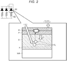
- FIG. 2 is a diagram illustrating a configuration and an operation principle of the SPAD.
- Each SPAD includes an APD 101 and a quench resistor 102.
- the quench resistor 102 is connected to a current output terminal of the APD 101.
- the APD 101 in the example in FIG. 2 includes a thick P-type semiconductor layer and a thin N-type semiconductor layer.
- the APD 101 includes a substrate SUB, a P-type semiconductor layer P, a P-plus-type semiconductor layer P + , and an N-plus-type semiconductor layer N + .
- the substrate SUB is a P-type semiconductor substrate.
- the P-type semiconductor layer P is stacked on the substrate SUB.
- the P-type semiconductor layer P is a thin P-type semiconductor layer having a lower impurity concentration than the P-plus-type semiconductor layer P + .
- the P-type semiconductor layer P may be thin epitaxial layer, for example.
- the P-plus-type semiconductor layer P + is a semiconductor layer in which a P-type impurity has a higher impurity concentration than the P-type semiconductor layer P.
- the N-plus-type semiconductor layer N + is a semiconductor layer of a high electron concentration in which an N-type impurity is introduced. Electrodes, not specifically illustrated, are formed in the N-plus-type semiconductor layer N + . A high reverse-bias voltage is applied to the APD 101 through the electrodes in a direction in which the substrate side is negative.
- a depletion layer D is formed near a junction region between the P-type semiconductor layer and the N-type semiconductor layer.
- an electron-positive hole pair as a carrier C L is generated in the depletion layer D.
- the carrier C L generated in the depletion layer D drifts due to an electric field E caused by the reverse-bias voltage.
- the electron is accelerated in the direction of the surface (N-plus-type semiconductor layer N + ), and the positive hole is accelerated in the direction of the substrate.
- the electron accelerated toward the N-plus-type semiconductor layer N + collides with an atom under a strong electric field near the PN junction.
- the electron colliding with the atom ionizes the atom and generates a new electron-positive hole pair.
- the reverse-bias voltage exceeds a breakdown voltage, the generation of the electron-positive hole pair is repeated.
- Such avalanche breakdown discharges the APD 101.
- Such discharge is called Geiger discharge. In such a manner, an electric signal related to the Geiger discharge and subsequent recovery is output from one SPAD.
- a current output from the APD 101 flows into the quench resistor 102.
- the bias voltage is decreased due to a decrease in voltage.
- the Geiger phenomenon stops.
- a flow of recovery current charging a capacitance such as a junction capacitance of the APD 101 ends, the current output stops.
- the Geiger phenomenon stops and the current output is reduced to a certain extent, the APD 101 returns to a state where subsequent light can be received.
- the APD 101 is not limited to the structure in FIG. 2 .
- the P-plus-type semiconductor layer P + may not be provided in all examples.
- the APD in FIG. 2 has a structure including a thick P-type semiconductor layer and a thin N-type semiconductor layer
- the APD may conversely have a structure including a thick N-type semiconductor layer and a thin P-type semiconductor layer.
- the PN junction may not be near the surface as depicted in FIG. 2 .
- the PN junction may be formed around a boundary between the substrate SUB and a layer formed thereon, such as P-type semiconductor layer P.
- FIG. 3A is a diagram illustrating a configuration example of one SPAD in the embodiment.
- one SPAD in the embodiment includes the APD, a first quench resistor Rq, a second resistor Rst, and a diode D as a rectification element.
- the APD is forwardly connected to a power supply, and a reverse-bias voltage Vsub is applied to the APD from the power supply, not illustrated, disposed in the substrate SUB.
- One end of the first quench resistor Rq is connected to a cathode of the APD.
- Another end of the first quench resistor Rq is connected to an output terminal Out1 of the sensor 33.
- the output terminal Out1 is connected to the second amplifier 35.
- the SPADs When SPADs are arranged in a multi-pixel form, the SPADs may form a group.
- the first quench resistor Rq of the SPAD belonging to a certain group is connected to the first quench resistor Rq of another SPAD belonging to the same group at a connection point A illustrated in FIG. 3A . Accordingly, an electric signal corresponding to the total of the outputs of the SPADs belonging to the group is output to the second amplifier 35 from the output terminal Out1.
- the second resistor Rst is connected in parallel with the first quench resistor Rq.
- a resistance value of the second resistor Rst is lower than a resistance value of the first quench resistor Rq.
- the resistance value of the first quench resistor Rq is 250 kQ
- the resistance value of the second resistor Rst is 2 kQ.
- the diode D is a rectification element forwardly connected to the second resistor Rst. That is, a cathode of the diode D as a current output terminal is connected to an output terminal Out2 of the sensor 33.
- the cathode of the diode D of the SPAD is connected to the cathode of another diode D at a connection point B illustrated in FIG. 3A . Accordingly, an electric signal corresponding to the total of the output of each diode D is output to the ground from the output terminal Out2.
- the diode D may be a Zener diode or an avalanche photodiode (which is different from the above-described APD) .
- the APD when light is incident on the APD, the APD causes avalanche breakdown and outputs a current signal.
- the current signal from the APD flows into the first quench resistor Rq. Since the second resistor and the diode D are connected in parallel with the first quench resistor, a voltage generated in the first quench resistor due to the current signal flowing into the first quench resistor Rq from the APD is applied to the second resistor and the diode D.
- a quantity of electricity I generated per unit time when light is incident on the APD is represented by Expression 1 below.
- I Np ⁇ PDE ⁇ G ⁇ e
- Np denotes the number of photons absorbed in the APD.
- the detection efficiency of the APD is denoted by PDE.
- the gain (amplification rate) of the APD is denoted by G.
- the elementary charge is denoted by e.
- the carrier generated in the APD is discharged in a case where I - Iq is equal to zero or is small enough to be regarded as zero. In this case, subsequent detection by the APD can be performed.
- I - Iq is equal to a significantly high large, the carrier generated in the APD remains for a long time before dissipation. While the carrier remains, the output of the APD continues. Thus, during such a period, a subsequent detection event cannot be performed by the APD.
- the second resistor Rst and the diode D are connected in parallel with the first quench resistor Rq. Accordingly, even when a high intensity of light is incident on the APD, the carrier generated in the APD is discharged in a relatively short time.
- the APD is forwardly connected to the power supply, and the reverse-bias voltage Vsub is applied to the APD from the power supply.
- the APD may be reversely connected to the power supply.
- the diode D may be reversely connected to the second resistor Rst. That is, the APD and the diode D may be connected in the same direction. Accordingly, when the APD is reversely connected to the power supply, the diode D is reversely connected to the second resistor Rst. In addition, when the APD is forwardly connected to the power supply, the diode D is forwardly connected to the second resistor Rst.
- FIG. 3A illustrates the diode D as a rectification element connected in parallel with the first quench resistor Rq.
- the rectification element is not limited to a diode.
- the diode D may be a Zener diode ZD.
- the breakdown voltage is 25 V (as typically represented as a positive number)
- the voltage of the output terminal Out1 is approximately 0 V
- an overvoltage operating the SPAD is 0 to -5 V (represented as 0 to 5 V without a minus sign)
- a Zener diode ZD having a breakdown voltage of 5 V or higher is used.
- the diode D may be an avalanche photodiode.
- the second resistor Rst restricts the current flowing into the Zener diode ZD (and the voltage applied between both ends of the Zener diode ZD) and prevents breakage of the Zener diode ZD.
- the second resistor Rst reduces the effect of a parasitic capacitance of the Zener diode ZD on the characteristics of the SPAD at the time of a typical operation.
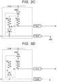
- FIG. 3D illustrates a circuit configuration in a case where the diode D is reversed.
- the power supply voltage Vsub is -30 V
- the breakdown voltage is 25 V (as typically represented as a positive number)
- the voltage of the output terminal Out1 is approximately 0 V
- the overvoltage operating the SPAD is 0 to -5 V (represented as 0 to 5 V without a minus sign)
- a specific voltage lower than or equal to - (5 V + threshold voltage of diode D) is applied to the output terminal Out2.
- a decrease in voltage caused by light exceeds the applied voltage, a current flows into the diode D, and the accumulated carrier is discharged.
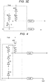
- the diode of FIG. 3D is replaced with a P-type MOS transistor Tr.
- the power supply voltage Vsub is -30 V
- the breakdown voltage is 25 V (as typically represented as a positive number)
- the voltage of the output terminal Out1 is approximately 0 V
- the overvoltage operating the SPAD is 0 to -5 V (represented as 0 to 5 V without a minus sign)
- a specific voltage lower than or equal to - (5 V + threshold voltage of transistor) is applied to the output terminal Out2.
- a decrease in voltage caused by light exceeds the applied voltage, a current flows into the transistor Tr, and the accumulated carrier is discharged.
- the carrier can be discharged in a small amount of time.
- the direction of the parasitic diode of the transistor Tr may be in reverse to the direction of the diode D. That is, in a case where the transistor Tr is a P-channel MOS transistor, a drain of the transistor Tr is connected to the second resistor Rst, and a source of the transistor Tr is connected to the output terminal Out2.
- FIG. 3C to FIG. 3E illustrate circuit configurations in a case where the APD has the structure in FIG. 2 and FIG. 3E illustrates a circuit configuration in a case where the APD is a P-channel MOS transistor
- the structure of the APD is not limited to those cases as described above.
- an N-channel MOS transistor may be used instead of the P-channel MOS transistor.
- Modification Example 3 will be described.
- the breakdown phenomenon of the rectification element is used for promoting the discharge of the carrier from the APD.
- the same effect can be achieved by forwardly connecting a plurality of diodes D1, D2 ... D3 to the second resistor Rst. That is, by forwardly connecting a plurality of diodes, a forward threshold voltage can be increased. By increasing the forward threshold voltage, a current does not flow at a low voltage, and a high current flows when a high voltage is applied as in the case of reversely connecting the diode. Accordingly, Modification Example 3 achieves the same effect as the above embodiment and Modification Example 1. Furthermore, when the APD is forwardly connected to the power supply, the plurality of diodes D1, D2 ... D3 may be reversely connected to the second resistor Rst.
- FIG. 5A is a diagram illustrating a structure of an SiPM of Modification Example 4.
- FIG. 5B illustrates an enlarged view of a region C in FIG. 5A .
- other SPADs also include the second resistor Rst having the same connection structure as FIG. 5B .
- the SiPM is formed by arranging the SPADs in a multi-pixel form.
- the SiPM includes a sensor region in which the SPAD including the APD and the first quench resistor Rq is 2-dimensionally arranged.
- the sensor region in the example in FIG. 5A is divided into two regions in the left-right direction of the page.
- the left-right direction is the horizontal direction when the sensor 33 is mounted in the distance measuring device 1.
- the first quench resistor Rq connected to the APD is arranged in a separation region that is the boundary of the SPAD in the left-right direction.
- the separation region is a region disposed between the SPADs in order not to propagate the carrier present in one of the adjacent SPADs to the other.
- the separation region may be light-shielded.
- the first quench resistor Rq in the SPAD of each row in the right half of the sensor region is connected to one horizontal wiring drawn out through a separation region that is the boundary of the SPAD in the up-down direction.
- the horizontal wiring of each row is connected to one vertical wiring at the right end of the sensor region.
- the vertical wiring is connected to the output terminal Out1.
- wiring of the SPAD is drawn out toward the left end of the sensor region.
- the first quench resistor Rq connected to the APD is arranged in a separation region that is the boundary of the SPAD in the left-right direction.
- the first quench resistor Rq in the SPAD of each row in the left half of the sensor region is connected to one horizontal wiring drawn out through a separation region that is the boundary of the SPAD in the up-down direction.
- the horizontal wiring of each row is connected to one vertical wiring at the left end of the sensor region.
- the vertical wiring is connected to another output terminal Out1.
- the second resistor Rst and the rectification element are connected to the first quench resistor Rq.
- the opening ratio of the SPAD that is, the light reception area of the APD, is decreased.
- the rectification element (for example, the diode D) is disposed at the end of the sensor region.
- the diode D of the SPAD in the right half region of the sensor region is collectively arranged at the right end of the sensor region.
- the diode D of the SPAD in the left half region of the sensor region is collectively arranged at the left end of the sensor region.
- Each diode D disposed at the right end of the sensor region is connected in common to the output terminal Out2 by wiring that is drawn out through the separation region.
- each diode D disposed at the left end of the sensor region is connected in common to another output terminal Out2 by wiring that is drawn out through the separation region.
- the sensor region is divided into two regions in the left-right direction in FIG. 5A
- the sensor region is not limited to FIG. 5A .
- the sensor region may be divided into two regions in the up-down direction.
- the diode D may be separately disposed at the upper end and the lower end of the sensor region.
- FIG. 6 is a diagram illustrating a structure of an SiPM of Modification Example 5.
- the diode D may be collectively arranged in a partial region of the sensor region in which the SPAD is to be disposed.
- the SPAD may be disposed in the sensor region excepting a region in which the diodes D are collectively arranged.
- the diodes D may be separately collected at two or more locations.
- FIG. 7 is a diagram illustrating an example of the second resistor Rst and the transistor Tr formed as the rectification element in a layer above the APD using a thin film transistor.
- a P-type semiconductor layer 202 is formed in a substrate 201.
- a P-plus-type semiconductor layer 203 and an N-plus-type semiconductor layer 204 are stacked in the P-type semiconductor layer 202.
- two electrodes 205a and 205b are formed in the N-plus-type semiconductor layer 204.
- the electrode 205a is connected to the power supply.
- the electrode 205b is connected to an electrode 210b of the transistor Tr constituting the second resistor Rst.
- the APD is formed by the P-type semiconductor layer 202, the P-plus-type semiconductor layer 203, the N-plus-type semiconductor layer 204, and the electrodes 205a and 205b.
- the surrounding area of the electrodes 205a and 205b is flattened by an insulating layer 206.
- An insulating layer 207 is stacked on the insulating layer 206.
- a semiconductor layer 208 formed of, for example, InGaZnO is formed in the insulating layer 207.
- the semiconductor layer 208 is connected to electrodes 210a and 210b of the transistor formed through an insulating layer 209.
- the electrode 210a is, for example, a source electrode of the transistor.
- the electrode 210b is, for example, a drain electrode.
- the second resistor is formed by the semiconductor layer 208 and the electrodes 210a and 210b.
- another semiconductor layer 211 formed of, for example, InGaZnO is formed in the insulating layer 207.
- the semiconductor layer 211 is connected to electrodes 212a and 212b of the transistor through the insulating layer 209.
- the electrode 212a is, for example, a source electrode of the transistor.
- the electrode 212b is, for example, a drain electrode.
- the electrode 210a and the electrode 212a are connected to each other.
- the transistor Tr as the rectification element is formed by the semiconductor layer 211 and the electrodes 212a and 212b.
- An insulating layer 213 as a protective layer is formed on the electrodes 210a, 210b, 212a, and 212b.
- the second resistor Rst and the transistor Tr may be formed in the same step.
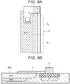
- FIG. 8A and FIG. 8B are diagrams illustrating an example of forming the diode D as the rectification element next to the APD using polysilicon.
- the diode D is connected to the APD through wiring W.
- the diode D includes a junction between a polysilicon layer Pp in which a P-type impurity is introduced and a polysilicon layer Pn in which an N-type impurity is introduced.
- the elements of the APD and the diode D are separated from each other by a local oxidation of silicon (LOCOS) layer.
- LOC local oxidation of silicon
- PDN denotes an N-plus-type semiconductor layer constituting the APD
- PDP denotes a P-plus-type semiconductor layer constituting the APD
- 1P - denotes a diffusion layer.
Landscapes
- Physics & Mathematics (AREA)
- Engineering & Computer Science (AREA)
- Electromagnetism (AREA)
- General Physics & Mathematics (AREA)
- Radar, Positioning & Navigation (AREA)
- Remote Sensing (AREA)
- Computer Networks & Wireless Communication (AREA)
- Light Receiving Elements (AREA)
- Optical Radar Systems And Details Thereof (AREA)
- Measurement Of Optical Distance (AREA)
Applications Claiming Priority (1)
| Application Number | Priority Date | Filing Date | Title |
|---|---|---|---|
| JP2019055105A JP7278821B2 (ja) | 2019-03-22 | 2019-03-22 | センサ及び距離計測装置 |
Publications (2)
| Publication Number | Publication Date |
|---|---|
| EP3712648A2 true EP3712648A2 (de) | 2020-09-23 |
| EP3712648A3 EP3712648A3 (de) | 2020-11-11 |
Family
ID=68847999
Family Applications (1)
| Application Number | Title | Priority Date | Filing Date |
|---|---|---|---|
| EP19214739.5A Pending EP3712648A3 (de) | 2019-03-22 | 2019-12-10 | Sensor und entfernungsmessvorrichtung |
Country Status (4)
| Country | Link |
|---|---|
| US (2) | US11662464B2 (de) |
| EP (1) | EP3712648A3 (de) |
| JP (1) | JP7278821B2 (de) |
| CN (1) | CN111796294B (de) |
Cited By (1)
| Publication number | Priority date | Publication date | Assignee | Title |
|---|---|---|---|---|
| EP4064350A1 (de) * | 2021-03-23 | 2022-09-28 | Kabushiki Kaisha Toshiba | Lichtdetektor |
Families Citing this family (6)
| Publication number | Priority date | Publication date | Assignee | Title |
|---|---|---|---|---|
| JP7337517B2 (ja) | 2019-03-14 | 2023-09-04 | 株式会社東芝 | 光検出器及び距離測定装置 |
| US11378663B2 (en) * | 2019-11-26 | 2022-07-05 | Waymo Llc | Systems and methods for biasing light detectors |
| US20240313022A1 (en) * | 2021-01-06 | 2024-09-19 | Sony Semiconductor Solutions Corporation | Light receiving element and ranging system |
| CN116106863A (zh) * | 2021-11-11 | 2023-05-12 | 上海禾赛科技有限公司 | 硅光电倍增管及其读出电路、读出方法和激光雷达 |
| CN118575286A (zh) | 2022-02-17 | 2024-08-30 | 索尼半导体解决方案公司 | 光电检测装置和光电检测装置的制造方法 |
| JP2024041597A (ja) * | 2022-09-14 | 2024-03-27 | 株式会社東芝 | 光検出器、光検出システム、ライダー装置、及び移動体 |
Family Cites Families (22)
| Publication number | Priority date | Publication date | Assignee | Title |
|---|---|---|---|---|
| IT1229945B (it) | 1988-10-20 | 1991-09-17 | Consiglio Nazionale Ricerche | Circuito di spegnimento attivo per fotodiodi a semiconduttore a valanga per singoli fotoni, adatto per il funzionamento con fotodiodo in posizione remota |
| GB8915245D0 (en) * | 1989-07-03 | 1989-08-23 | Secr Defence | Avalanche photodiode quenching circuit |
| US5532474A (en) * | 1993-12-17 | 1996-07-02 | Eg&G Limited | Active quench circuit and reset circuit for avalanche photodiode |
| US6525305B2 (en) | 2000-09-11 | 2003-02-25 | Perkinelmer Canada, Inc. | Large current watchdog circuit for a photodetector |
| US6522396B1 (en) * | 2002-01-08 | 2003-02-18 | Raytheon Company | Dual mode adaptive threshold architecture for 3-D ladar FPA |
| JP2006303524A (ja) * | 2006-06-08 | 2006-11-02 | Oki Comtec Ltd | アバランシェフォトダイオード用バイアス電圧制御回路およびその調整方法 |
| CN201497580U (zh) * | 2009-09-21 | 2010-06-02 | 安徽问天量子科技股份有限公司 | 吉赫兹脉冲门控低通滤波红外单光子探测器 |
| JP5739753B2 (ja) * | 2011-07-08 | 2015-06-24 | 株式会社 ニコンビジョン | 距離測定装置 |
| JP6017916B2 (ja) * | 2012-10-16 | 2016-11-02 | 株式会社豊田中央研究所 | 光検出器 |
| CA2931055C (en) | 2013-11-22 | 2022-07-12 | Ottomotto Llc | Lidar scanner calibration |
| JP6193171B2 (ja) | 2014-04-11 | 2017-09-06 | 株式会社東芝 | 光検出器 |
| US9720109B2 (en) * | 2014-12-24 | 2017-08-01 | General Electric Company | Systems and methods for minimizing silicon photomultiplier signal propagation delay dispersion and improve timing |
| CN105047517B (zh) * | 2015-07-08 | 2017-11-14 | 武汉京邦科技有限公司 | 一种数字光电倍增器件 |
| US9985071B2 (en) * | 2016-04-15 | 2018-05-29 | Qualcomm Incorporated | Active area selection for LIDAR receivers |
| CN106411299B (zh) * | 2016-09-27 | 2019-03-05 | 杭州电子科技大学 | 一种高速单光子雪崩二极管淬灭复位电路 |
| US10338224B2 (en) | 2017-03-27 | 2019-07-02 | Analog Devices Global Unlimited Company | High dynamic range analog front-end receiver for long range LIDAR |
| WO2018183715A1 (en) * | 2017-03-29 | 2018-10-04 | Luminar Technologies, Inc. | Method for controlling peak and average power through laser receiver |
| CN107063453B (zh) * | 2017-04-07 | 2018-08-10 | 电子科技大学 | 一种负载可变的单光子雪崩光电二极管淬灭电路 |
| EP3419168B1 (de) * | 2017-06-23 | 2020-12-02 | ams AG | Lawinendiodenanordnung und verfahren zur steuerung einer lawinendiodenanordnung |
| US11136215B2 (en) | 2017-08-21 | 2021-10-05 | Teltech Group Llc | Tether cable spooling apparatus |
| JP2020031180A (ja) * | 2018-08-24 | 2020-02-27 | パイオニア株式会社 | 検出装置及びセンサ装置 |
| CN109494278B (zh) * | 2019-01-10 | 2024-07-26 | 深圳技术大学(筹) | 主动式淬灭电路以及脉冲式tof传感器 |
-
2019
- 2019-03-22 JP JP2019055105A patent/JP7278821B2/ja active Active
- 2019-07-29 CN CN201910686095.XA patent/CN111796294B/zh active Active
- 2019-08-30 US US16/556,490 patent/US11662464B2/en active Active
- 2019-12-10 EP EP19214739.5A patent/EP3712648A3/de active Pending
-
2023
- 2023-04-10 US US18/297,875 patent/US12007481B2/en active Active
Cited By (2)
| Publication number | Priority date | Publication date | Assignee | Title |
|---|---|---|---|---|
| EP4064350A1 (de) * | 2021-03-23 | 2022-09-28 | Kabushiki Kaisha Toshiba | Lichtdetektor |
| US12159954B2 (en) | 2021-03-23 | 2024-12-03 | Kabushiki Kaisha Toshiba | Light detector |
Also Published As
| Publication number | Publication date |
|---|---|
| JP7278821B2 (ja) | 2023-05-22 |
| EP3712648A3 (de) | 2020-11-11 |
| CN111796294B (zh) | 2024-07-05 |
| US11662464B2 (en) | 2023-05-30 |
| US20230243969A1 (en) | 2023-08-03 |
| JP2020153929A (ja) | 2020-09-24 |
| CN111796294A (zh) | 2020-10-20 |
| US20200300621A1 (en) | 2020-09-24 |
| US12007481B2 (en) | 2024-06-11 |
Similar Documents
| Publication | Publication Date | Title |
|---|---|---|
| US12007481B2 (en) | Sensor and distance measuring device | |
| US11275156B2 (en) | Sensor and distance measuring device comprising first and second quenching devices respectively connected to current output terminals of fist and second avalanche photodiodes | |
| CN107665886B (zh) | 用于检测红外线辐射的盖革模式雪崩光电二极管阵列 | |
| EP3385987A1 (de) | Festkörperbildgebungselement und bildgebungsvorrichtung | |
| US20220082668A1 (en) | Light detector and distance measurement device | |
| US12159954B2 (en) | Light detector | |
| JP6663167B2 (ja) | 光検出装置 | |
| US11527670B2 (en) | Photon avalanche diode and methods of producing thereof | |
| US12328960B2 (en) | Photosensor and distance measurement system | |
| US20170263793A1 (en) | Photodetector and object detection system using the same | |
| US10782428B1 (en) | Light receiving device and distance measuring apparatus | |
| JP2019057567A (ja) | 光検出器、光検出装置、ライダー装置及び光検出器の製造方法 | |
| JP6862386B2 (ja) | 光検出器、ライダー装置、及び光検出器の製造方法 | |
| JP6847878B2 (ja) | 光検出器、光検出装置及びライダー装置 | |
| US11139326B2 (en) | Photodetector, photodetection device, laser imaging detection and ranging apparatus | |
| CN114551603B (zh) | 一种雪崩光电二极管 | |
| JP2024016609A (ja) | 光検出器及び距離計測装置 | |
| Isaak et al. | Design and characterisation of 16× 1 parallel outputs SPAD array in 0.18 um CMOS technology | |
| JP2024035593A (ja) | 光検出器及び距離計測装置 | |
| CN117374087A (zh) | 光电探测器及单光子探测系统 | |
| JP2022133698A (ja) | 半導体装置 |
Legal Events
| Date | Code | Title | Description |
|---|---|---|---|
| PUAI | Public reference made under article 153(3) epc to a published international application that has entered the european phase |
Free format text: ORIGINAL CODE: 0009012 |
|
| STAA | Information on the status of an ep patent application or granted ep patent |
Free format text: STATUS: THE APPLICATION HAS BEEN PUBLISHED |
|
| AK | Designated contracting states |
Kind code of ref document: A2 Designated state(s): AL AT BE BG CH CY CZ DE DK EE ES FI FR GB GR HR HU IE IS IT LI LT LU LV MC MK MT NL NO PL PT RO RS SE SI SK SM TR |
|
| AX | Request for extension of the european patent |
Extension state: BA ME |
|
| PUAL | Search report despatched |
Free format text: ORIGINAL CODE: 0009013 |
|
| AK | Designated contracting states |
Kind code of ref document: A3 Designated state(s): AL AT BE BG CH CY CZ DE DK EE ES FI FR GB GR HR HU IE IS IT LI LT LU LV MC MK MT NL NO PL PT RO RS SE SI SK SM TR |
|
| AX | Request for extension of the european patent |
Extension state: BA ME |
|
| RIC1 | Information provided on ipc code assigned before grant |
Ipc: G01S 17/14 20200101ALN20201007BHEP Ipc: G01S 7/4863 20200101AFI20201007BHEP Ipc: H01L 27/146 20060101ALI20201007BHEP Ipc: G01S 17/42 20060101ALN20201007BHEP |
|
| STAA | Information on the status of an ep patent application or granted ep patent |
Free format text: STATUS: REQUEST FOR EXAMINATION WAS MADE |
|
| 17P | Request for examination filed |
Effective date: 20210422 |
|
| RBV | Designated contracting states (corrected) |
Designated state(s): AL AT BE BG CH CY CZ DE DK EE ES FI FR GB GR HR HU IE IS IT LI LT LU LV MC MK MT NL NO PL PT RO RS SE SI SK SM TR |
|
| STAA | Information on the status of an ep patent application or granted ep patent |
Free format text: STATUS: EXAMINATION IS IN PROGRESS |
|
| 17Q | First examination report despatched |
Effective date: 20230313 |