EP3711079B1 - Rf-energieversorgung für vakuumplasmaverarbeitung - Google Patents
Rf-energieversorgung für vakuumplasmaverarbeitung Download PDFInfo
- Publication number
- EP3711079B1 EP3711079B1 EP18793418.7A EP18793418A EP3711079B1 EP 3711079 B1 EP3711079 B1 EP 3711079B1 EP 18793418 A EP18793418 A EP 18793418A EP 3711079 B1 EP3711079 B1 EP 3711079B1
- Authority
- EP
- European Patent Office
- Prior art keywords
- impedance
- plasma processing
- vacuum plasma
- processing module
- impedance transform
- Prior art date
- Legal status (The legal status is an assumption and is not a legal conclusion. Google has not performed a legal analysis and makes no representation as to the accuracy of the status listed.)
- Active
Links
Images




Classifications
-
- H—ELECTRICITY
- H01—ELECTRIC ELEMENTS
- H01J—ELECTRIC DISCHARGE TUBES OR DISCHARGE LAMPS
- H01J37/00—Discharge tubes with provision for introducing objects or material to be exposed to the discharge, e.g. for the purpose of examination or processing thereof
- H01J37/32—Gas-filled discharge tubes
- H01J37/32009—Arrangements for generation of plasma specially adapted for examination or treatment of objects, e.g. plasma sources
- H01J37/32082—Radio frequency generated discharge
- H01J37/32174—Circuits specially adapted for controlling the RF discharge
- H01J37/32183—Matching circuits
-
- H—ELECTRICITY
- H01—ELECTRIC ELEMENTS
- H01J—ELECTRIC DISCHARGE TUBES OR DISCHARGE LAMPS
- H01J37/00—Discharge tubes with provision for introducing objects or material to be exposed to the discharge, e.g. for the purpose of examination or processing thereof
- H01J37/02—Details
- H01J37/18—Vacuum locks ; Means for obtaining or maintaining the desired pressure within the vessel
-
- H—ELECTRICITY
- H01—ELECTRIC ELEMENTS
- H01J—ELECTRIC DISCHARGE TUBES OR DISCHARGE LAMPS
- H01J37/00—Discharge tubes with provision for introducing objects or material to be exposed to the discharge, e.g. for the purpose of examination or processing thereof
- H01J37/32—Gas-filled discharge tubes
-
- H—ELECTRICITY
- H01—ELECTRIC ELEMENTS
- H01J—ELECTRIC DISCHARGE TUBES OR DISCHARGE LAMPS
- H01J37/00—Discharge tubes with provision for introducing objects or material to be exposed to the discharge, e.g. for the purpose of examination or processing thereof
- H01J37/32—Gas-filled discharge tubes
- H01J37/32009—Arrangements for generation of plasma specially adapted for examination or treatment of objects, e.g. plasma sources
- H01J37/32082—Radio frequency generated discharge
-
- H—ELECTRICITY
- H01—ELECTRIC ELEMENTS
- H01J—ELECTRIC DISCHARGE TUBES OR DISCHARGE LAMPS
- H01J37/00—Discharge tubes with provision for introducing objects or material to be exposed to the discharge, e.g. for the purpose of examination or processing thereof
- H01J37/32—Gas-filled discharge tubes
- H01J37/32009—Arrangements for generation of plasma specially adapted for examination or treatment of objects, e.g. plasma sources
- H01J37/32082—Radio frequency generated discharge
- H01J37/32174—Circuits specially adapted for controlling the RF discharge
-
- H—ELECTRICITY
- H01—ELECTRIC ELEMENTS
- H01J—ELECTRIC DISCHARGE TUBES OR DISCHARGE LAMPS
- H01J37/00—Discharge tubes with provision for introducing objects or material to be exposed to the discharge, e.g. for the purpose of examination or processing thereof
- H01J37/32—Gas-filled discharge tubes
- H01J37/32431—Constructional details of the reactor
- H01J37/32532—Electrodes
- H01J37/32577—Electrical connecting means
-
- H—ELECTRICITY
- H01—ELECTRIC ELEMENTS
- H01J—ELECTRIC DISCHARGE TUBES OR DISCHARGE LAMPS
- H01J37/00—Discharge tubes with provision for introducing objects or material to be exposed to the discharge, e.g. for the purpose of examination or processing thereof
- H01J37/32—Gas-filled discharge tubes
- H01J37/32431—Constructional details of the reactor
- H01J37/32798—Further details of plasma apparatus not provided for in groups H01J37/3244 - H01J37/32788; special provisions for cleaning or maintenance of the apparatus
- H01J37/32899—Multiple chambers, e.g. cluster tools
-
- H—ELECTRICITY
- H01—ELECTRIC ELEMENTS
- H01J—ELECTRIC DISCHARGE TUBES OR DISCHARGE LAMPS
- H01J2237/00—Discharge tubes exposing object to beam, e.g. for analysis treatment, etching, imaging
- H01J2237/002—Cooling arrangements
Definitions
- Rf (radio frequency) power is customarily supplied to vacuum plasma processing modules- be it as power for supplying the plasma discharge and/or power for biasing an electrode e.g. a workpiece carrier electrode, separate from discharge electrodes- in that a matchbox is provided which matches the output impedance of a RF power supply generator to the input impedance of the vacuum processing module.
- a vacuum plasma processing module is e.g. a sputtering module, an etching module, an electron-beam deposition module, a PECVD module (Plasma Enhanced Chemical Deposition) or even a cathodic arc evaporation module.
- Rf power may be supplied for supplying the plasma discharge or for, more generically, just for biasing an electrode participating to the processing, as e.g. a substrate carrier electrode.
- the matchbox has costumery the ability of fast and automatic adapting matching to the momentarily prevailing input impedance of the vacuum plasma processing module.
- the input impedances of vacuum plasma processing modules are different and behave different even if such modules considered are of the same type, e.g. sputtering modules, but are differently operated, e.g. with different material target, in different gaseous atmospheres etc.
- vacuum plasma processing modules Throughout the present description we refer to vacuum plasma processing modules to be different, if their input impedances are different and/or behave differently over time.
- a frequency being a radio frequency (RF) if it is at least 1 MHz.
- a matchbox assigned to a respective vacuum plasma processing module is customarily mounted directly to the supplied vacuum plasma processing module, handles the high RF currents to be supplied to the respective vacuum plasma processing module and performs fast, automatic impedance matching.
- Different vacuum plasma processing modules are operated via the respective number of such match boxes specifically tailored for the respective vacuum plasma processing module.
- US 2006 0017386 discloses an apparatus for providing a fixed impedance transformation network for driving a plasma chamber includes a pre-match network adapted to couple between an Active RF match network and a plasma chamber load associated with the plasma chamber.
- the pre-match network includes a first capacitive element, an inductive element connected in parallel with the first capacitive element to form a parallel circuit, and a second capacitive element coupled to the parallel circuit.
- US 7 042 311 discloses a system for delivering radio frequency (RF) power to a plasma processing system includes an automatic impedance matching network configured to receive RF power from an RF generator, and a fixed impedance matching network coupled between the automatic impedance matching network and the plasma processing chamber.
- RF radio frequency
- WO 02 059933 discloses a plasma processing system with a plasma chamber in which a workpiece support member is arranged.
- the workpiece support is connected to a RF power supply by means of a first capacitive element and a first inductive element that are arranged on the workpiece support in the plasma chamber and are which are immersed within a coolant and by means of a second capacitive element and a second inductive element that are arranged outside of the plasma chamber, wherein the second inductive element can be a hollow copper tubing in which coolant is flowing.
- EP 0 597 497 discloses matching networks to a load which network comprise variable inductive elements, which are cooled by their core in a cooling jacket through which a coolant can be circulated.
- the windings may be cooled by passing coolant through hollow conductors forming the windings.
- a method of RF power delivering from a RF supply generator to at least one vacuum plasma processing module comprising time varying matching the output impedance of the RF supply generator to the input impedance of the vacuum plasma processing module by a) Providing in the vacuum plasma processing module an impedance transform network and performing by this impedance transform network a time invariant impedance transform of the input impedance of the vacuum plasma processing module to an input impedance to the impedance transform network; b) Performing time variable matching of the output impedance of the RF supply generator to the input impedance of the impedance transform network by a matchbox operationally connected to the impedance transform network.
- One variant of the method according to the invention comprises performing by the impedance transform network a current compensation so as to deliver to a vacuum plasma process operated in the vacuum plasma processing module a current which is larger than a supply current supplied to the input of the impedance transform network from the RF supply generator.
- One variant of the method according to the invention comprises interconnecting the output of the RF supply generator and the impedance transform network comprising interconnecting by a transmission line and, in a further embodiment, the addressed interconnecting comprises interconnecting by a coaxial cable.
- constructing the impedance transform network comprises providing inductive and capacitive elements which are all discrete and passive elements.
- At least some parts of the impedance transform network are cooled.
- One variant of the method according to the invention comprises providing at least a part of at least one inductive element of said impedance transform network by a hollow conductor and flowing a cooling medium through said hollow conductor.
- said cooling, medium is additionally flown through a cooling arrangement of a part of the vacuum plasma processing module which is not a part of the impedance transform network.
- One variant of the method according to the invention comprises RF power delivering from said RF supply generator to at least two of said vacuum plasma processing modules via a single, central matchbox.
- One variant of the method according to the invention comprises RF power delivering from the RF supply generator, consecutively, to at least two of the vacuum plasma processing modules and performing, consecutively, at least time variable matching of the output impedance of the RF supply generator to the input impedances of the at least two impedance transform networks by a single, central matchbox.
- matchbox which performs automatically the fast matching adaptation to the respective time varying part of the input impedances of the at least two impedance transform networks as provided in the at least two vacuum plasma processing modules.
- One variant of the just addressed variant of the method according to the invention comprises performing by at least one of the at least two impedance transform networks a current compensation, so as to deliver to a vacuum plasma process performed in the respective vacuum plasma processing module a current which is larger than a supply current supplied to the at least one respective impedance transform network from the RF supply generator.
- one variant of the method according to the invention comprises performing a respective one of the addressed current compensation at both of said at least two impedance transform networks.
- interconnecting the output of the RF supply generator and at least one of the at least two impedance transform networks comprises interconnecting by a transmission line, thereby, and in a further variant, interconnecting by the transmission line comprises interconnecting by a coaxial cable.
- interconnecting the output of the RF supply generator and each of the at least two impedance transform networks comprises interconnecting by a respective transmission line, whereby each of said transmission lines may comprise a coaxial cable.
- constructing the at least two impedance transform networks comprises providing inductive and capacitive elements which are all discrete and passive elements.
- One variant of the method according to the invention comprises performing by each of the respective at least two impedance transform networks a respective time invariant impedance transform of the respective input impedance of the respective vacuum plasma processing module to a respective desired input impedance to the respective impedance transform network, time invariant components of the absolute values of resulting, desired input impedances being in a desired or predetermined range or being mutually neglectably different or being equal.
- the method according to the invention comprises the at least two vacuum plasma processing modules are different in the sense as we have defined above.
- One variant of the method according to the invention comprises RF supplying by the impedance transform network of said at least one vacuum plasma processing module at least one of a plasma discharge current to the at least one vacuum plasma processing module and of providing RF biasing or workpiece RF biasing to the at least one vacuum plasma processing module.
- the at least one vacuum plasma processing module is one of a sputtering module, an etching module, a PECVD layer deposition module, a cathodic arc evaporation module, a plasma evaporation module, an electron beam evaporation module.
- One variant of the method according to the invention comprises performing by the impedance transform network a current compensation by means of a shunt impedance
- One variant of the method according to the invention comprises connecting an electrode for plasma processing to more than one output of the impedance transform network. Thereby and in one variant, distribution of RF currents at said more than one outputs is selected or selectable.
- the method according to the invention may also be considered under the aspect of being a method for manufacturing vacuum plasma treated workpieces.
- the method according to the invention may be realized by means of an apparatus or plant as addressed in the following.
- a RF vacuum plasma processing module comprising a time invariant impedance transform network between an RF supply input and at least one of a plasma discharge electrode and of a RF biased electrode for the vacuum plasma processing.
- the time invariant impedance transform network comprises inductive and capacitive elements, all being discrete and passive elements.
- the time invariant impedance transform network is constructed to supply a RF current to the addressed electrode which is larger than a RF supply current input to the time invariant impedance transform network.
- the time invariant impedance transform network thus performs current compensation.
- the time invariant impedance transform network comprises a cooling arrangement.
- the time invariant impedance transform network comprises at least one inductive element at least a part thereof being realized as a hollow conductor.
- the hollow conductor is flow-connectable, or flow connected to at least one of a flow-source and of a flow-drain for a cooling fluid.
- a flow-source a device where the flow originates
- a flow-drain a device where the flow goes to.
- the cooling arrangement at the time invariant impedance transform network comprises a hollow body, e.g. at least a part of an inductive element realized as a hollow conductor, flow connected to a source and/or a drain for a cooling fluid, the hollow body being in cooling fluid communication with a part of the vacuum plasma processing module which is not part of said time invariant impedance transform network.
- the time invariant impedance transform network is manually tunable.
- the time invariant impedance transform network has more than one RF current output.
- the more than one RF current outputs are connected to the electrode, i.e. to the same electrode.
- One embodiment of the RF vacuum plasma processing module according to the invention is one of a sputter module, an etching module, a PECVD module, a cathodic arc evaporation module, a plasma evaporation module, an electron-beam evaporation module.
- Two or more than two embodiments of the RF vacuum plasma processing module according to the invention may be combined, if not contradictory.
- a plasma treatment plant comprising at least two of the RF vacuum plasma processing modules according to the invention or according to one or more than one of its embodiments, and at least one RF supply generator operatively connected to a match box, the RF output of the matchbox being operatively connected to the RF inputs of both time invariant impedance transform networks of the at least two vacuum plasma processing modules.
- the match box is constructed to perform automatic, time variant matching to the input impedances of both of said time invariant impedance transform networks.
- One embodiment of the plasma treatment plant according to the invention comprises a switch unit and a timing control unit operationally connected to a control input of said switch unit, said switch unit being constructed to switch RF power supply consecutively to said at least two time invariant impedance transform networks.
- the at least two vacuum plasma processing modules are different modules, different being defined as addressed above.
- the Rf power supply connection from the RF power generator to the at least two time invariant impedance transform networks comprises at least one transmission line.
- the addressed transmission line comprises at least one coaxial cable.
- each of the time invariable impedance transform networks of the at least two vacuum plasma processing modules is constructed to provide its input impedance so as to comprise a time invariant impedance part, the absolute value of the time invariant impedance parts of the at least two time invariant impedance networks being in a desired range or being only neglectably different or being equal.
- the match box is remote from the at least two vacuum plasma processing modules.
- the invention is further directed to a method of manufacturing a substrate treated by a RF supplied vacuum plasma treatment by means of a method according to the invention or according to one or more than one variant thereof and /or by a module according to the invention or one or more than one embodiment thereof and/or by a plant according to the invention or one or more than one embodiments thereof.
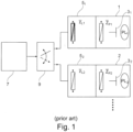
- Fig.1 shows, by means of a simplified signal-flow/ functional-block diagram, prior art RF power delivery to RF operated vacuum plasma process modules 1, 2,... , called VPPM.
- the VPPM 1,2,... are e.g. sputtering modules, etching modules, PECVD modules, cathodic arc evaporation modules, plasma evaporation modules electron beam evaporation modules, generically VPPM at which the plasma discharge-PL-electrode is RF supplied and/ or another electrode e.g. a workpiece carrier electrode is RF biased.
- Such electrodes are addressed in fig.1 by by 3 1,2,.. to which Rf power is applied.
- the VPPM or at least a part of the processing modules 1,2,.. are different in that, in operation, they present at the Rf power input different or over time differently behaving complex input impedances Z P1 , Z P2... .
- time invariant impedance part Z Pxo may be freely selected e.g. as that impedance value which is momentarily present when initiating the respective vacuum plasma process, or e.g. as an average impedance value of the time varying Z Px (t) over the processing timespan.
- the time invariant part Z Pxo may be regarded as an impedance working point and the time varying part ⁇ Z Px (t) as momentary deviation of Z Px (t) about the impedance working point. (Please note that the impedances Z are complex entities).
- a dedicated match box 5 1,2,. is narrowly coupled to each VPPM 1,2...
- Each match box 5 1,2, . transforms the respective input impedance Z Px (t) in an input impedance Z Lx to the match box 5 x from which the impedance seen from a RF supply power generator 7 is dependent.
- Customarily the Z Lx impedances are made as equal as possible and may be addressed by Z L . This necessitates that every match box 5 x is constructed to perform automatic fast impedance transform.
- the match boxes 5 x match a predetermined impedance Z L to the respective impedances Z Px (t).
- a switch 9 distributes, consecutively, the Rf power from the Rf supply power generator 7 to the respective match boxes 5 1,2.. , i.e. 5 x .
- a dedicated match box 5 x is hooked to every VPPM x ,matching the output impedance of the RF power generator e.g. of 50 ⁇ to the respective input impedances of the VPPM x .
- the match boxes do all include fast automatic matching ability so as to take time variations of the respective impedances Z Px (t) into account.
- At least a part of the time invariant matching is performed by including a time invariant impedance transform network 1 T , 2 T ..X T in the respective VPPM 1,2...X .
- VPPM 1 o , 2 o ...X o is obtained by including a time invariant impedance transform network 1 T , 2 T ..X T in the respective VPPM 1,2...X .
- the time invariant impedance transform networks consist of passive and discrete inductive elements L 1T , 2T , .. XT and of passive, discrete capacitive elements C 1T,2T,..XT , with spurious or discrete resistive elements R (not shown in Fig.2 ).
- the TITN 1 T ,2 T,... are constructed so, that the absolute values of the time invariant parts Z T ⁇ (complex entities) of all VPPM 1 o ,2 o... are in a predetermined impedance-range or are only neglectably different or are even equal.
- Consecutive RF power distribution from RF power supply generator 7 to the VPPM 1o,2o,... is realized c via a single, central matchbox 11 and a switch 9.
- the switch which may be incorporated in the match box 11and is controlled by a timer unit 10.
- the match box 11 performs matching of the generator output impedance to the input impedances Z 1T , 2T...XT and thus performs all the fast, automatic time variable matching. If necessary the match box 11 additionally performs remaining time invariant matching, if the Z To of the VPPM 1 o ,2 o... are still not tolerably different and/or the Z To does not accord with the output impedance of the Rf power supply generator 7.
- modules 1 o , 2 o... . which incorporate a passive TITN of inductive and capacitive discrete elements between the respective RF input and the respective process electrode 3 1 ,3 2 .. of the VPPM 1 o ,2 o... ..
- the concept according to the invention may be considered of splitting overall matching between a RF power supply generator and multiple, different VPPM, on one hand in decentralized, module- dedicated time invariant impedance transforming and, on the other hand, in a central matching at least performing time varying, module specific matching, possibly additionally some time invariant matching.
- the remaining central matchbox 11 may be provided remote from the VPPM 1 o , 2 o... , in opposition to prior art matchboxes 5 1,2... which are to be mounted directly to the respective VPPM 1,2...
- the Rf currents to be supplied to the VPPM 1,2,... may be quite large up to 100A rms and even more.
- Such high currents are to be considered along the supply connection of RF power to the VPPM 1 o , 2o, ... .
- Fig. 3 shows generically a current compensation network as may be exploited in one embodiment of the CTITN 1 T , 2 T , ... X T .
- Fig.4 shows an example of realizing such current compensation and impedance transform network, as addressed now called CTITN 1 T , 2 T , ... .
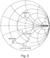
- Fig 5 shows the respective smith chart representation.
- a current compensation impedance Z cc which shunts the Rf input, via impedance Z ca , for the supply current i ca .
- the compensation current i cc is added to the current i ca to result in a current i PL .
- both impedances Z ca and Z cc are complex, proper tailoring of the compensation impedance Z cc in the CTITN leads to the fact that the real part of i PL becomes larger than the real part of i ca .
- the time invariant impedance transform networks perform impedance transform as desired as well as current compensation.
- the discrete inductive and capacitive elements of CTITN 1 T , 2 T , ... may therefore be dimensioned for standing high currents, higher than the current i ca from the Rf supply generator and the elements of the central matchbox 11 as well as the connection lines from the Rf generator 7 to the match box 11 and via switch 9 to the CTITN 1 T and/or 2 T and/ or ... . may be tailored for standing lower currents.
- the power connection lines from the RF power generator 7 up to at least one or to all of the CTITN 1 T , 2 T , ... or at least a part of these RF power connection lines 13a, 13b, 13c (see fig.2 ) may therefore be realized by transmission lines including coaxial cable.
- the discrete elements of the CTITN 1 T , 2 T , ... are tailored for the high currents there may occur on one hand the need of cooling such networks.
- a cooling fluid provided for cooling the respective VPPN is also flown through parts of the TITN or CTITN for cooling such parts. Possibly no additional cooling ability may be needed at the central match box 11.
- Inductors of the TITN or of the CTITN or parts thereof may be realized by hollow tube conductors, and are thus perfectly suited to flow a gaseous or liquid cooling medium therethrough, especially that medium which also flows through parts of the VPPM 1,2,...
- Most flexible interconnection of a remote central matchbox 11, via the switch 9, to the remote VPPM 1 o , 2 o ,.. is performed by means of coaxial cables, e.g. 50 ⁇ cables as transmission lines. These cables or similar transmission lines may not be conceived for currents as high as RF currents supplying the VPPM 1,2, for the respective vacuum plasma process therein.
- the cable should be loaded by 25 ⁇ minimum.
- the impedance Z P1 (see Fig.2 )
- the reactor load or input impedance is transformed by the addressed time invariant impedance transform network CTITN 1 T into the 2:1 VSWR-circle (Voltage Standing Wave Ratio).
- the cable becomes loaded with a negative real impedance of less than 25 ⁇ .
- the current through the current compensation and transform network CTITN 1 T of the VPPM 1 o will add to the current through the cable, resulting in a current to the process in processing module VPPN 1 of e.g. 30 A rms .
- tapping off the shunt capacitor C c2 along the inductance L cc may be manually shifted in the CTITN so as to perform fine tuning.
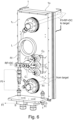
- Fig.6 shows a CTITN 1 T of a VPPM 1 o , namely of a square sputtering module
- the inductivity L is realized as a pipe to flow the liquid cooling fluid Fl which is also fed to the target mount of VPPM 1 o for cooling same.
- the flow path of the cooling fluid Fl from source S to drain D is schematically shown in fig.6 in dash line.
- the electric network of the CTITN 1 T is represented in fig 7 . Transformation tuning may e.g. be realized by simply exchanging the inductivity pipe for L.
- Fig. 8 shows the impedances Z Pxo of sputter modules 1,2,3 according to fig. 6 for Al2O3, ITO and Al targets.
- Fig. 9 shows the transformation performed in principle by the LC transform network 1 T of fig. 7 and fig. 10 shows the resulting practically identical Z To .
- Fig.11 shows, in analogy to the representation of fig.6 a realization example of CTITN 1 T at a circular sputtering module VPPM 1 o .
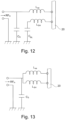
- Fig.12 shows the electrical network of the CTITN 1 T as realized at VPPM 1 o of fig.11 .
- the fluid Fl output from inductivity pipe L SE is linked to the fluid input to the inductivity pipe L SH by an electrically isolating tube schematically shown at IT in dash dotted line.
- the path of cooling fluid Fl is again shown in dashed line.
- the target 20 may be Rf supplied at more than one locus, and the Rf current distribution to these loci may be adjusted by respectively selecting the values of L Se and L SH .
- An equal Rf current to the supply loci at the target 20 may be achieved by electrically connecting the Fl-out end of the inductivity pipe L Se with the Fl -in end of the inductivity pipe L SH as represented in fig.13 .
Landscapes
- Chemical & Material Sciences (AREA)
- Analytical Chemistry (AREA)
- Physics & Mathematics (AREA)
- Engineering & Computer Science (AREA)
- Plasma & Fusion (AREA)
- Plasma Technology (AREA)
- Physical Vapour Deposition (AREA)
- Chemical Vapour Deposition (AREA)
- Drying Of Semiconductors (AREA)
Claims (25)
- Verfahren zur Abgabe von RF-Leistung von einem RF-Versorgungsgenerator (7) an mindestens ein Vakuumplasmaverarbeitungsmodul (1o,2o), umfassend eine zeitvariable Angleichung der Ausgangsimpedanz des RF-Versorgungsgenerators an die Eingangsimpedanz des Vakuumplasmaverarbeitungsmoduls durcha) Bereitstellen eines Impedanztransformationsnetzwerks (1T,2T) im Vakuumplasmaverarbeitungsmodul und Durchführen einer zeitinvarianten Impedanztransformation der Eingangsimpedanz des Vakuumplasmaverarbeitungsmoduls in eine Eingangsimpedanz des Impedanztransformationsnetzwerks durch das Impedanztransformationsnetzwerk;b) Durchführen einer zeitvariablen Angleichung der Ausgangsimpedanz des RF-Versorgungsgenerators an die Eingangsimpedanz des Impedanztransformationsnetzwerks (1T,2T) durch eine Angleichungsbox (11), die operativ mit dem Impedanztransformationsnetzwerk verbunden ist;c) Bereitstellen mindestens eines Teils mindestens eines induktiven Elements des Impedanztransformationsnetzwerks durch einen Hohlleiter und Durchströmen des Hohlleiters und einer Kühlanordnung eines Teils des Vakuumplasmabearbeitungsmoduls, der nicht Teil des Impedanztransformationsnetzwerks ist, mit einem Kühlmedium.
- Das Verfahren nach Anspruch 1 umfasst ferner die Durchführung einer Stromkompensation durch das Impedanztransformationsnetzwerk, um einen Vakuumplasmaprozess, der im Vakuumplasmaverarbeitungsmodul durchgeführt wird, mit einem Strom zu versorgen, der grösser ist als ein Versorgungsstrom, der dem Impedanztransformationsnetzwerk vom RF-Versorgungsgenerator zugeführt wird.
- Verfahren nach mindestens einem der Ansprüche 1 und 2, bei dem das Impedanztransformationsnetzwerk so aufgebaut wird, dass induktive und kapazitive Elemente bereitgestellt werden, die alle diskrete und passive Elemente sind.
- Das Verfahren nach mindestens einem der Ansprüche 1 bis 3 umfasst die Abgabe von RF-Leistung vom RF-Versorgungsgenerator an mindestens ein weiteres Vakuumplasmaverarbeitungsmodul, das ebenfalls das Impedanztransformationsnetzwerk aufweist, über eine gemeinsame zentrale Angleichungsbox.
- Verfahren nach mindestens einem der Ansprüche 1 bis 4, umfassend das Liefern von RF-Leistung vom RF-Versorgungsgenerator nacheinander an das eine VakuumplasmaBearbeitungsmodul und an ein weiteres VakuumplasmaBearbeitungsmodul, das ebenfalls das Impedanztransformationsnetzwerk umfasst, und Durchführen mindestens einer zeitvariable Angleichung der Ausgangsimpedanz des RF-Versorgungsgenerators an die jeweilige Eingangsimpedanz der mindestens zwei Impedanztransformationsnetzwerke der mindestens zwei Vakuumplasma-Bearbeitungsmodule durch eine einzige, zentrale Angleichungsbox.
- Verfahren nach mindestens einem der Ansprüche 4 oder 5, umfassend die Durchführung einer jeweiligen zeitinvarianten Impedanztransformation der jeweiligen Eingangsimpedanz des jeweiligen Vakuumplasmaverarbeitungsmoduls in eine jeweilige gewünschte Eingangsimpedanz in das jeweilige Impedanztransformationsnetzwerk durch jedes der mindestens zwei Impedanztransformationsnetzwerke, wobei die zeitinvarianten Komponenten der Absolutwerte der gewünschten Eingangsimpedanzen in einem gewünschten Bereich liegen oder vernachlässigbar unterschiedlich oder gleich sind.
- Verfahren nach mindestens einem der Ansprüche 4 bis 6, wobei die mindestens zwei Vakuumplasmabearbeitungsmodule unterschiedlich sind.
- Verfahren nach mindestens einem der Ansprüche 1 bis 7, wobei es sich bei dem mindestens einen Vakuumplasmabearbeitungsmodul um eines der folgenden Module handelt: ein Sputtermodul, ein Ätzmodul, ein PECVD-Schichtabscheidungsmodul, ein Kathodenbogenverdampfungsmodul, ein Plasmaverdampfungsmodul und ein Elektronenstrahlverdampfungsmodul.
- Verfahren nach mindestens einem der Ansprüche 1 bis 8, umfassend das Verbinden einer Elektrode zur Plasmabehandlung an mehr als einen Ausgang des Impedanztransformationsnetzwerks.
- Das Verfahren nach Anspruch 9, umfasst das Auswählen der Verteilung der RF-Ströme an den mehr als einen Ausgängen.
- Das Verfahren nach mindestens einem der Ansprüche 1 bis 10 zur Herstellung eines vakuumplasmabehandelten Werkstücks.
- Ein RF-Vakuumplasmaverarbeitungsmodul (1o,2o), umfassend ein zeitinvariantes Impedanztransformationsnetzwerk (1T,2T) zwischen einem RF-Versorgungseingang und einer Plasmaentladungselektrode und/oder einer RF-vorgespannten Elektrode für die Vakuumplasmaverarbeitung, wobei das zeitinvariante Impedanztransformationsnetzwerk mindestens ein induktives Element umfasst, von dem mindestens ein Teil als Hohlleiter ausgeführt ist, wobei der Hohlleiter mit einer Strömungsquelle und/oder einer Strömungsableitung für ein Kühlfluid strömungsverbindbar oder strömungsverbunden ist, wobei der Hohlleiter in Kühlfluidströmungsverbindung mit einer Kühlanordnung für einen Teil des Vakuumplasmabearbeitungsmoduls steht, der nicht Teil des zeitinvarianten Impedanztransformationsnetzwerks ist.
- Das RF-Vakuumplasmaverarbeitungsmodul nach Anspruch 12, wobei das zeitinvariante Impedanztransformationsnetzwerk aufgebaut ist, um der Elektrode einen RF-Strom zuzuführen, der grösser ist als ein RF-Versorgungsstrom, der dem zeitinvarianten Impedanztransformationsnetzwerk zugeführt wird.
- Das RF-Vakuumplasmaverarbeitungsmodul nach mindestens einem der Ansprüche 12 oder 13, wobei das zeitinvariante Impedanztransformationsnetzwerk manuell abstimmbar ist.
- Das RF-Vakuumplasmaverarbeitungsmodul nach mindestens einem der Ansprüche 12 bis 14, wobei das zeitinvariante Impedanztransformationsnetzwerk mehr als einen RF-Stromausgang aufweist.
- Das RF-Vakuumplasmabearbeitungsmodul nach Anspruch 15, wobei die mehr als einen HF-Stromausgänge mit der Elektrode verbunden sind.
- Das HF-Vakuumplasmabearbeitungsmodul nach mindestens einem der Ansprüche 12 bis 16 ist eines der folgenden Module: ein Sputtermodul, ein Ätzmodul, ein PECVD-Knötchen, ein Kathodenbogenverdampfungsmodul, ein Plasmaverdampfungsmodul, ein Elektronenstrahlverdampfungsmodul.
- Eine Plasmabehandlungsanlage umfassend mindestens zwei RF-Vakuumplasmaverarbeitungsmodulen, von denen mindestens eines einem der Ansprüche 12 bis 17 entspricht und das andere ebenfalls das zeitinvariante Impedanztransformationsnetzwerk umfasst, mindestens einen RF-Versorgungsgenerator, der operativ mit einer Angleichungsbox verbunden ist, wobei der RF-Ausgang der Angleichungsbox operativ mit den RF-Eingängen der beiden zeitinvarianten Impedanztransformationsnetzwerken der mindestens zwei Vakuumplasmaverarbeitungsmodule verbunden ist.
- Die Plasmabehandlungsanlage nach Anspruch 18, wobei die Angleichungsbox konstruiert ist, um eine automatische, zeitvariante Anpassung an die Eingangsimpedanzen der beiden zeitinvarianten Impedanztransformationsnetzwerke durchzuführen.
- Die Plasmabehandlungsanlage nach mindestens einem der Ansprüche 18 oder 19 ferner umfassend eine Schalteinheit und eine Zeitsteuerungseinheit, die operativ mit einem Steuereingang der Schalteinheit verbunden ist, wobei die Schalteinheit aufgebaut ist, um die RF-Stromversorgung nacheinander auf die mindestens zwei zeitinvarianten Impedanztransformationsnetzwerke zu schaltet.
- Die Plasmabehandlungsanlage nach mindestens einem der Ansprüche 18 bis 20, wobei die mindestens zwei Vakuumplasmabehandlungsmodule unterschiedliche Module sind.
- Die Plasmabehandlungsanlage nach mindestens einem der Ansprüche 18 bis 21, wobei jedes der zeitinvarianten Impedanztransformationsnetzwerke der mindestens zwei Vakuumplasmaverarbeitungsmodule aufgebaut ist, um seine Eingangsimpedanz mit einem zeitinvarianten Impedanzteil bereitzustellen, wobei der Absolutwert der zeitinvarianten Impedanzteile der mindestens zwei zeitinvarianten Impedanznetzwerke in einem gewünschten Bereich liegt oder nur vernachlässigbar unterschiedlich oder gleich ist.
- Die Plasmabehandlungsanlage nach mindestens einem der Ansprüche 18 bis 22, wobei die Angleichungsbox von den mindestens zwei Vakuumplasmabehandlungsmodulen entfernt ist.
- Das Verfahren nach mindestens einem der Ansprüche 1 bis 11, durchgeführt mit einem Gerät oder einer Anlage nach mindestens einem der Ansprüche 12 bis 23.
- Ein Verfahren zur Herstellung eines Substrats, das durch eine RF-gespeiste Vakuumplasmabehandlung mittels eines Verfahrens nach mindestens einem der Ansprüche 1 bis 11 oder 24 und/oder eines Moduls nach mindestens einem der Ansprüche 12 bis 17 und/oder einer Anlage nach mindestens einem der Ansprüche 18 bis 23 behandelt wurde.
Applications Claiming Priority (2)
| Application Number | Priority Date | Filing Date | Title |
|---|---|---|---|
| CH13932017 | 2017-11-17 | ||
| PCT/EP2018/079424 WO2019096564A1 (en) | 2017-11-17 | 2018-10-26 | Rf power delivery to vacuum plasma processing |
Publications (2)
| Publication Number | Publication Date |
|---|---|
| EP3711079A1 EP3711079A1 (de) | 2020-09-23 |
| EP3711079B1 true EP3711079B1 (de) | 2023-07-05 |
Family
ID=64017378
Family Applications (1)
| Application Number | Title | Priority Date | Filing Date |
|---|---|---|---|
| EP18793418.7A Active EP3711079B1 (de) | 2017-11-17 | 2018-10-26 | Rf-energieversorgung für vakuumplasmaverarbeitung |
Country Status (7)
| Country | Link |
|---|---|
| US (1) | US11380520B2 (de) |
| EP (1) | EP3711079B1 (de) |
| JP (1) | JP7330182B2 (de) |
| KR (1) | KR102424953B1 (de) |
| CN (1) | CN111316396B (de) |
| TW (1) | TWI783068B (de) |
| WO (1) | WO2019096564A1 (de) |
Families Citing this family (33)
| Publication number | Priority date | Publication date | Assignee | Title |
|---|---|---|---|---|
| WO2019096564A1 (en) * | 2017-11-17 | 2019-05-23 | Evatec Ag | Rf power delivery to vacuum plasma processing |
| US12288673B2 (en) | 2017-11-29 | 2025-04-29 | COMET Technologies USA, Inc. | Retuning for impedance matching network control |
| RU2020129100A (ru) * | 2018-02-20 | 2022-03-21 | ЭРЛИКОН МЕТКО (ЮЭс) ИНК. | Однодуговой каскадный плазмотрон низкого давления, использующий пакет нейтродов как способ контроля плазменной дуги |
| US10998209B2 (en) | 2019-05-31 | 2021-05-04 | Applied Materials, Inc. | Substrate processing platforms including multiple processing chambers |
| US11527385B2 (en) | 2021-04-29 | 2022-12-13 | COMET Technologies USA, Inc. | Systems and methods for calibrating capacitors of matching networks |
| US11114279B2 (en) | 2019-06-28 | 2021-09-07 | COMET Technologies USA, Inc. | Arc suppression device for plasma processing equipment |
| US11107661B2 (en) | 2019-07-09 | 2021-08-31 | COMET Technologies USA, Inc. | Hybrid matching network topology |
| US11596309B2 (en) | 2019-07-09 | 2023-03-07 | COMET Technologies USA, Inc. | Hybrid matching network topology |
| US12002611B2 (en) | 2019-08-28 | 2024-06-04 | COMET Technologies USA, Inc. | High power low frequency coils |
| US11670488B2 (en) | 2020-01-10 | 2023-06-06 | COMET Technologies USA, Inc. | Fast arc detecting match network |
| US11521832B2 (en) | 2020-01-10 | 2022-12-06 | COMET Technologies USA, Inc. | Uniformity control for radio frequency plasma processing systems |
| US12027351B2 (en) | 2020-01-10 | 2024-07-02 | COMET Technologies USA, Inc. | Plasma non-uniformity detection |
| US11887820B2 (en) | 2020-01-10 | 2024-01-30 | COMET Technologies USA, Inc. | Sector shunts for plasma-based wafer processing systems |
| US11830708B2 (en) | 2020-01-10 | 2023-11-28 | COMET Technologies USA, Inc. | Inductive broad-band sensors for electromagnetic waves |
| US11961711B2 (en) | 2020-01-20 | 2024-04-16 | COMET Technologies USA, Inc. | Radio frequency match network and generator |
| US11605527B2 (en) | 2020-01-20 | 2023-03-14 | COMET Technologies USA, Inc. | Pulsing control match network |
| US12080571B2 (en) | 2020-07-08 | 2024-09-03 | Applied Materials, Inc. | Substrate processing module and method of moving a workpiece |
| US11749542B2 (en) | 2020-07-27 | 2023-09-05 | Applied Materials, Inc. | Apparatus, system, and method for non-contact temperature monitoring of substrate supports |
| US11817331B2 (en) | 2020-07-27 | 2023-11-14 | Applied Materials, Inc. | Substrate holder replacement with protective disk during pasting process |
| US11600507B2 (en) | 2020-09-09 | 2023-03-07 | Applied Materials, Inc. | Pedestal assembly for a substrate processing chamber |
| US11610799B2 (en) | 2020-09-18 | 2023-03-21 | Applied Materials, Inc. | Electrostatic chuck having a heating and chucking capabilities |
| US11373844B2 (en) | 2020-09-28 | 2022-06-28 | COMET Technologies USA, Inc. | Systems and methods for repetitive tuning of matching networks |
| US12195314B2 (en) | 2021-02-02 | 2025-01-14 | Applied Materials, Inc. | Cathode exchange mechanism to improve preventative maintenance time for cluster system |
| US11674227B2 (en) | 2021-02-03 | 2023-06-13 | Applied Materials, Inc. | Symmetric pump down mini-volume with laminar flow cavity gas injection for high and low pressure |
| US12057296B2 (en) | 2021-02-22 | 2024-08-06 | COMET Technologies USA, Inc. | Electromagnetic field sensing device |
| US12002668B2 (en) | 2021-06-25 | 2024-06-04 | Applied Materials, Inc. | Thermal management hardware for uniform temperature control for enhanced bake-out for cluster tool |
| US11923175B2 (en) | 2021-07-28 | 2024-03-05 | COMET Technologies USA, Inc. | Systems and methods for variable gain tuning of matching networks |
| JP2025508466A (ja) * | 2022-02-24 | 2025-03-26 | ラム リサーチ コーポレーション | 基板処理システム用のrfアセンブリ |
| US12243717B2 (en) | 2022-04-04 | 2025-03-04 | COMET Technologies USA, Inc. | Variable reactance device having isolated gate drive power supplies |
| US12040139B2 (en) | 2022-05-09 | 2024-07-16 | COMET Technologies USA, Inc. | Variable capacitor with linear impedance and high voltage breakdown |
| US11657980B1 (en) | 2022-05-09 | 2023-05-23 | COMET Technologies USA, Inc. | Dielectric fluid variable capacitor |
| US12051549B2 (en) | 2022-08-02 | 2024-07-30 | COMET Technologies USA, Inc. | Coaxial variable capacitor |
| US12132435B2 (en) | 2022-10-27 | 2024-10-29 | COMET Technologies USA, Inc. | Method for repeatable stepper motor homing |
Family Cites Families (35)
| Publication number | Priority date | Publication date | Assignee | Title |
|---|---|---|---|---|
| CH568673A5 (de) * | 1974-03-15 | 1975-10-31 | Bbc Brown Boveri & Cie | |
| US4679007A (en) | 1985-05-20 | 1987-07-07 | Advanced Energy, Inc. | Matching circuit for delivering radio frequency electromagnetic energy to a variable impedance load |
| DE3632340C2 (de) * | 1986-09-24 | 1998-01-15 | Leybold Ag | Induktiv angeregte Ionenquelle |
| DE3927324A1 (de) | 1989-08-18 | 1991-02-21 | Leybold Ag | Kuehlvorrichtung fuer elektrische schaltungsanordnungen |
| JPH0720039B2 (ja) * | 1991-03-28 | 1995-03-06 | 株式会社芝浦製作所 | 高周波インピ−ダンス整合回路 |
| US5392018A (en) * | 1991-06-27 | 1995-02-21 | Applied Materials, Inc. | Electronically tuned matching networks using adjustable inductance elements and resonant tank circuits |
| US5572710A (en) * | 1992-09-11 | 1996-11-05 | Kabushiki Kaisha Toshiba | High speed logic simulation system using time division emulation suitable for large scale logic circuits |
| US6313587B1 (en) * | 1998-01-13 | 2001-11-06 | Fusion Lighting, Inc. | High frequency inductive lamp and power oscillator |
| US6211498B1 (en) * | 1999-03-01 | 2001-04-03 | Powell Power Electronics, Inc. | Induction heating apparatus and transformer |
| US6284110B1 (en) | 1999-04-14 | 2001-09-04 | Tokyo Electron Limited | Method and apparatus for radio frequency isolation of liquid heat transfer medium supply and discharge lines |
| US6376978B1 (en) * | 2000-03-06 | 2002-04-23 | The Regents Of The University Of California | Quartz antenna with hollow conductor |
| AU2002227418A1 (en) * | 2001-01-22 | 2002-08-06 | Tokyo Electron Limited | Vertically translatable chuck assembly and method for a plasma reactor system |
| US20040027209A1 (en) * | 2002-08-09 | 2004-02-12 | Applied Materials, Inc. | Fixed matching network with increased match range capabilities |
| JP3846881B2 (ja) * | 2003-04-04 | 2006-11-15 | 日本エー・エス・エム株式会社 | プラズマ処理装置及びシリコン酸化膜を形成する方法 |
| US7042311B1 (en) * | 2003-10-10 | 2006-05-09 | Novellus Systems, Inc. | RF delivery configuration in a plasma processing system |
| US7570130B2 (en) * | 2004-07-12 | 2009-08-04 | Applied Materials, Inc. | Apparatus and methods for a fixed impedance transformation network for use in connection with a plasma chamber |
| US8187416B2 (en) * | 2005-05-20 | 2012-05-29 | Applied Materials, Inc. | Interior antenna for substrate processing chamber |
| US7301343B1 (en) * | 2006-12-18 | 2007-11-27 | General Electric Co. | System, method and apparatus for controlling the temperature of a MRI magnet warm bore |
| FR2921538B1 (fr) * | 2007-09-20 | 2009-11-13 | Air Liquide | Dispositifs generateurs de plasma micro-ondes et torches a plasma |
| US8834969B2 (en) * | 2007-10-24 | 2014-09-16 | Oerlikon Advanced Technologies Ag | Method for manufacturing workpieces and apparatus |
| JP5554099B2 (ja) * | 2010-03-18 | 2014-07-23 | 東京エレクトロン株式会社 | プラズマ処理装置及びプラズマ処理方法 |
| US8920597B2 (en) * | 2010-08-20 | 2014-12-30 | Applied Materials, Inc. | Symmetric VHF source for a plasma reactor |
| US8416008B2 (en) | 2011-01-20 | 2013-04-09 | Advanced Energy Industries, Inc. | Impedance-matching network using BJT switches in variable-reactance circuits |
| JP2013105543A (ja) * | 2011-11-10 | 2013-05-30 | Tokyo Electron Ltd | 基板処理装置 |
| US10157729B2 (en) * | 2012-02-22 | 2018-12-18 | Lam Research Corporation | Soft pulsing |
| US9694990B2 (en) * | 2012-06-14 | 2017-07-04 | Evatec Ag | Transport and handing-over arrangement for disc-shaped substrates, vacuum treatment installation and method for manufacture treated substrates |
| US9082589B2 (en) * | 2012-10-09 | 2015-07-14 | Novellus Systems, Inc. | Hybrid impedance matching for inductively coupled plasma system |
| CN105102671B (zh) * | 2013-02-08 | 2020-08-07 | 瑞士艾发科技 | Hipims溅射的方法和hipims溅射系统 |
| US9460894B2 (en) * | 2013-06-28 | 2016-10-04 | Lam Research Corporation | Controlling ion energy within a plasma chamber |
| US9508529B2 (en) * | 2014-10-23 | 2016-11-29 | Lam Research Corporation | System, method and apparatus for RF power compensation in a plasma processing system |
| JP6424120B2 (ja) * | 2015-03-23 | 2018-11-14 | 東京エレクトロン株式会社 | 電源システム、プラズマ処理装置及び電源制御方法 |
| KR101777762B1 (ko) | 2015-09-03 | 2017-09-12 | 에이피시스템 주식회사 | 고주파 전원 공급장치 및 이를 포함하는 기판 처리장치 |
| JP2017098323A (ja) * | 2015-11-19 | 2017-06-01 | 東京エレクトロン株式会社 | プラズマエッチング方法 |
| JP6865128B2 (ja) * | 2017-07-19 | 2021-04-28 | 東京エレクトロン株式会社 | プラズマ処理装置 |
| WO2019096564A1 (en) * | 2017-11-17 | 2019-05-23 | Evatec Ag | Rf power delivery to vacuum plasma processing |
-
2018
- 2018-10-26 WO PCT/EP2018/079424 patent/WO2019096564A1/en not_active Ceased
- 2018-10-26 US US16/763,575 patent/US11380520B2/en active Active
- 2018-10-26 JP JP2020526940A patent/JP7330182B2/ja active Active
- 2018-10-26 CN CN201880074118.5A patent/CN111316396B/zh active Active
- 2018-10-26 KR KR1020207017565A patent/KR102424953B1/ko active Active
- 2018-10-26 TW TW107138031A patent/TWI783068B/zh active
- 2018-10-26 EP EP18793418.7A patent/EP3711079B1/de active Active
Also Published As
| Publication number | Publication date |
|---|---|
| TW201927079A (zh) | 2019-07-01 |
| JP2021503689A (ja) | 2021-02-12 |
| EP3711079A1 (de) | 2020-09-23 |
| TWI783068B (zh) | 2022-11-11 |
| US20210358718A1 (en) | 2021-11-18 |
| KR102424953B1 (ko) | 2022-07-25 |
| CN111316396B (zh) | 2023-02-17 |
| JP7330182B2 (ja) | 2023-08-21 |
| WO2019096564A1 (en) | 2019-05-23 |
| US11380520B2 (en) | 2022-07-05 |
| CN111316396A (zh) | 2020-06-19 |
| KR20200089711A (ko) | 2020-07-27 |
Similar Documents
| Publication | Publication Date | Title |
|---|---|---|
| US11380520B2 (en) | RF power delivery to vacuum plasma processing | |
| EP3817517B1 (de) | Plasmabehandlungsvorrichtung, plasmabehandlungsverfahren, programm und speichermedium | |
| US6888313B2 (en) | Impedance matching network with termination of secondary RF frequencies | |
| CN117612918A (zh) | 用于基座的rf接地配置 | |
| CN114521276A (zh) | 包含变压器和/或变压器耦合组合器的射频分配电路 | |
| JP2017050859A (ja) | 高周波電源供給装置及びこれを備える基板処理装置 | |
| JP2012529750A5 (de) | ||
| KR102432150B1 (ko) | 플라즈마 프로세싱 시스템들을 위한 소형의 구성 가능한 모듈형 무선 주파수 매칭 네트워크 조립체 | |
| CN111224626A (zh) | 宽带功率组合布置 | |
| CN100511357C (zh) | 与等离子体腔室连接的固定的阻抗变换网络的装置和方法 | |
| US11621147B2 (en) | Systems and methods for optimizing RF plasma power coupling | |
| CN109659217A (zh) | 用于多等离子处理腔的射频系统 | |
| US20030192475A1 (en) | Method and apparatus for routing harmonics in a plasma to ground within a plasma enhanced semiconductor wafer processing chamber | |
| US20050223990A1 (en) | Plasma processing system and its substrate processing process, plasma enhanced chemical vapor deposition system and its film deposition process | |
| JP3759519B2 (ja) | 高周波電力分配装置 | |
| KR20110134217A (ko) | 다중 분할 전극 세트를 위한 급전장치를 구비한 플라즈마 챔버 | |
| DE112005000627B4 (de) | Plasmabehandlung grossvolumiger Bauteile | |
| DE10015699B4 (de) | Schaltungsanordnung zur Impedanzkompensation | |
| CN109913854B (zh) | 等离子化学气相沉积装置 | |
| Lee et al. | Development of multiple inductively coupled plasma sources using coaxial transmission line for large-area processes | |
| TWI716831B (zh) | 可切換匹配網路及電感耦合電漿處理器 | |
| CN106486333B (zh) | 一种等离子体处理装置 | |
| JP2007107076A (ja) | 真空処理装置、真空処理装置による製膜方法 | |
| KR100994501B1 (ko) | 플라즈마 처리장치 | |
| WO2025172132A1 (de) | Hf-generator für ein plasmabearbeitungssystem und ein solches plasmabearbeitungssystem |
Legal Events
| Date | Code | Title | Description |
|---|---|---|---|
| STAA | Information on the status of an ep patent application or granted ep patent |
Free format text: STATUS: UNKNOWN |
|
| STAA | Information on the status of an ep patent application or granted ep patent |
Free format text: STATUS: THE INTERNATIONAL PUBLICATION HAS BEEN MADE |
|
| PUAI | Public reference made under article 153(3) epc to a published international application that has entered the european phase |
Free format text: ORIGINAL CODE: 0009012 |
|
| STAA | Information on the status of an ep patent application or granted ep patent |
Free format text: STATUS: REQUEST FOR EXAMINATION WAS MADE |
|
| 17P | Request for examination filed |
Effective date: 20200407 |
|
| AK | Designated contracting states |
Kind code of ref document: A1 Designated state(s): AL AT BE BG CH CY CZ DE DK EE ES FI FR GB GR HR HU IE IS IT LI LT LU LV MC MK MT NL NO PL PT RO RS SE SI SK SM TR |
|
| AX | Request for extension of the european patent |
Extension state: BA ME |
|
| DAV | Request for validation of the european patent (deleted) | ||
| DAX | Request for extension of the european patent (deleted) | ||
| STAA | Information on the status of an ep patent application or granted ep patent |
Free format text: STATUS: EXAMINATION IS IN PROGRESS |
|
| 17Q | First examination report despatched |
Effective date: 20211110 |
|
| GRAP | Despatch of communication of intention to grant a patent |
Free format text: ORIGINAL CODE: EPIDOSNIGR1 |
|
| STAA | Information on the status of an ep patent application or granted ep patent |
Free format text: STATUS: GRANT OF PATENT IS INTENDED |
|
| INTG | Intention to grant announced |
Effective date: 20230322 |
|
| GRAS | Grant fee paid |
Free format text: ORIGINAL CODE: EPIDOSNIGR3 |
|
| GRAA | (expected) grant |
Free format text: ORIGINAL CODE: 0009210 |
|
| STAA | Information on the status of an ep patent application or granted ep patent |
Free format text: STATUS: THE PATENT HAS BEEN GRANTED |
|
| AK | Designated contracting states |
Kind code of ref document: B1 Designated state(s): AL AT BE BG CH CY CZ DE DK EE ES FI FR GB GR HR HU IE IS IT LI LT LU LV MC MK MT NL NO PL PT RO RS SE SI SK SM TR |
|
| P01 | Opt-out of the competence of the unified patent court (upc) registered |
Effective date: 20230526 |
|
| REG | Reference to a national code |
Ref country code: CH Ref legal event code: EP |
|
| REG | Reference to a national code |
Ref country code: AT Ref legal event code: REF Ref document number: 1585625 Country of ref document: AT Kind code of ref document: T Effective date: 20230715 |
|
| REG | Reference to a national code |
Ref country code: DE Ref legal event code: R096 Ref document number: 602018052898 Country of ref document: DE |
|
| REG | Reference to a national code |
Ref country code: IE Ref legal event code: FG4D |
|
| REG | Reference to a national code |
Ref country code: LT Ref legal event code: MG9D |
|
| REG | Reference to a national code |
Ref country code: NL Ref legal event code: MP Effective date: 20230705 |
|
| REG | Reference to a national code |
Ref country code: AT Ref legal event code: MK05 Ref document number: 1585625 Country of ref document: AT Kind code of ref document: T Effective date: 20230705 |
|
| PG25 | Lapsed in a contracting state [announced via postgrant information from national office to epo] |
Ref country code: NL Free format text: LAPSE BECAUSE OF FAILURE TO SUBMIT A TRANSLATION OF THE DESCRIPTION OR TO PAY THE FEE WITHIN THE PRESCRIBED TIME-LIMIT Effective date: 20230705 |
|
| PG25 | Lapsed in a contracting state [announced via postgrant information from national office to epo] |
Ref country code: GR Free format text: LAPSE BECAUSE OF FAILURE TO SUBMIT A TRANSLATION OF THE DESCRIPTION OR TO PAY THE FEE WITHIN THE PRESCRIBED TIME-LIMIT Effective date: 20231006 |
|
| PG25 | Lapsed in a contracting state [announced via postgrant information from national office to epo] |
Ref country code: ES Free format text: LAPSE BECAUSE OF FAILURE TO SUBMIT A TRANSLATION OF THE DESCRIPTION OR TO PAY THE FEE WITHIN THE PRESCRIBED TIME-LIMIT Effective date: 20230705 |
|
| PG25 | Lapsed in a contracting state [announced via postgrant information from national office to epo] |
Ref country code: IS Free format text: LAPSE BECAUSE OF FAILURE TO SUBMIT A TRANSLATION OF THE DESCRIPTION OR TO PAY THE FEE WITHIN THE PRESCRIBED TIME-LIMIT Effective date: 20231105 |
|
| PG25 | Lapsed in a contracting state [announced via postgrant information from national office to epo] |
Ref country code: SE Free format text: LAPSE BECAUSE OF FAILURE TO SUBMIT A TRANSLATION OF THE DESCRIPTION OR TO PAY THE FEE WITHIN THE PRESCRIBED TIME-LIMIT Effective date: 20230705 Ref country code: RS Free format text: LAPSE BECAUSE OF FAILURE TO SUBMIT A TRANSLATION OF THE DESCRIPTION OR TO PAY THE FEE WITHIN THE PRESCRIBED TIME-LIMIT Effective date: 20230705 Ref country code: PT Free format text: LAPSE BECAUSE OF FAILURE TO SUBMIT A TRANSLATION OF THE DESCRIPTION OR TO PAY THE FEE WITHIN THE PRESCRIBED TIME-LIMIT Effective date: 20231106 Ref country code: NO Free format text: LAPSE BECAUSE OF FAILURE TO SUBMIT A TRANSLATION OF THE DESCRIPTION OR TO PAY THE FEE WITHIN THE PRESCRIBED TIME-LIMIT Effective date: 20231005 Ref country code: LV Free format text: LAPSE BECAUSE OF FAILURE TO SUBMIT A TRANSLATION OF THE DESCRIPTION OR TO PAY THE FEE WITHIN THE PRESCRIBED TIME-LIMIT Effective date: 20230705 Ref country code: LT Free format text: LAPSE BECAUSE OF FAILURE TO SUBMIT A TRANSLATION OF THE DESCRIPTION OR TO PAY THE FEE WITHIN THE PRESCRIBED TIME-LIMIT Effective date: 20230705 Ref country code: IS Free format text: LAPSE BECAUSE OF FAILURE TO SUBMIT A TRANSLATION OF THE DESCRIPTION OR TO PAY THE FEE WITHIN THE PRESCRIBED TIME-LIMIT Effective date: 20231105 Ref country code: HR Free format text: LAPSE BECAUSE OF FAILURE TO SUBMIT A TRANSLATION OF THE DESCRIPTION OR TO PAY THE FEE WITHIN THE PRESCRIBED TIME-LIMIT Effective date: 20230705 Ref country code: GR Free format text: LAPSE BECAUSE OF FAILURE TO SUBMIT A TRANSLATION OF THE DESCRIPTION OR TO PAY THE FEE WITHIN THE PRESCRIBED TIME-LIMIT Effective date: 20231006 Ref country code: FI Free format text: LAPSE BECAUSE OF FAILURE TO SUBMIT A TRANSLATION OF THE DESCRIPTION OR TO PAY THE FEE WITHIN THE PRESCRIBED TIME-LIMIT Effective date: 20230705 Ref country code: ES Free format text: LAPSE BECAUSE OF FAILURE TO SUBMIT A TRANSLATION OF THE DESCRIPTION OR TO PAY THE FEE WITHIN THE PRESCRIBED TIME-LIMIT Effective date: 20230705 Ref country code: AT Free format text: LAPSE BECAUSE OF FAILURE TO SUBMIT A TRANSLATION OF THE DESCRIPTION OR TO PAY THE FEE WITHIN THE PRESCRIBED TIME-LIMIT Effective date: 20230705 |
|
| PG25 | Lapsed in a contracting state [announced via postgrant information from national office to epo] |
Ref country code: PL Free format text: LAPSE BECAUSE OF FAILURE TO SUBMIT A TRANSLATION OF THE DESCRIPTION OR TO PAY THE FEE WITHIN THE PRESCRIBED TIME-LIMIT Effective date: 20230705 |
|
| REG | Reference to a national code |
Ref country code: DE Ref legal event code: R097 Ref document number: 602018052898 Country of ref document: DE |
|
| PG25 | Lapsed in a contracting state [announced via postgrant information from national office to epo] |
Ref country code: SM Free format text: LAPSE BECAUSE OF FAILURE TO SUBMIT A TRANSLATION OF THE DESCRIPTION OR TO PAY THE FEE WITHIN THE PRESCRIBED TIME-LIMIT Effective date: 20230705 Ref country code: RO Free format text: LAPSE BECAUSE OF FAILURE TO SUBMIT A TRANSLATION OF THE DESCRIPTION OR TO PAY THE FEE WITHIN THE PRESCRIBED TIME-LIMIT Effective date: 20230705 Ref country code: EE Free format text: LAPSE BECAUSE OF FAILURE TO SUBMIT A TRANSLATION OF THE DESCRIPTION OR TO PAY THE FEE WITHIN THE PRESCRIBED TIME-LIMIT Effective date: 20230705 Ref country code: DK Free format text: LAPSE BECAUSE OF FAILURE TO SUBMIT A TRANSLATION OF THE DESCRIPTION OR TO PAY THE FEE WITHIN THE PRESCRIBED TIME-LIMIT Effective date: 20230705 Ref country code: CZ Free format text: LAPSE BECAUSE OF FAILURE TO SUBMIT A TRANSLATION OF THE DESCRIPTION OR TO PAY THE FEE WITHIN THE PRESCRIBED TIME-LIMIT Effective date: 20230705 Ref country code: SK Free format text: LAPSE BECAUSE OF FAILURE TO SUBMIT A TRANSLATION OF THE DESCRIPTION OR TO PAY THE FEE WITHIN THE PRESCRIBED TIME-LIMIT Effective date: 20230705 |
|
| PLBE | No opposition filed within time limit |
Free format text: ORIGINAL CODE: 0009261 |
|
| STAA | Information on the status of an ep patent application or granted ep patent |
Free format text: STATUS: NO OPPOSITION FILED WITHIN TIME LIMIT |
|
| PG25 | Lapsed in a contracting state [announced via postgrant information from national office to epo] |
Ref country code: IT Free format text: LAPSE BECAUSE OF FAILURE TO SUBMIT A TRANSLATION OF THE DESCRIPTION OR TO PAY THE FEE WITHIN THE PRESCRIBED TIME-LIMIT Effective date: 20230705 Ref country code: MC Free format text: LAPSE BECAUSE OF FAILURE TO SUBMIT A TRANSLATION OF THE DESCRIPTION OR TO PAY THE FEE WITHIN THE PRESCRIBED TIME-LIMIT Effective date: 20230705 |
|
| REG | Reference to a national code |
Ref country code: CH Ref legal event code: PL |
|
| 26N | No opposition filed |
Effective date: 20240408 |
|
| REG | Reference to a national code |
Ref country code: BE Ref legal event code: MM Effective date: 20231031 |
|
| PG25 | Lapsed in a contracting state [announced via postgrant information from national office to epo] |
Ref country code: LU Free format text: LAPSE BECAUSE OF NON-PAYMENT OF DUE FEES Effective date: 20231026 |
|
| GBPC | Gb: european patent ceased through non-payment of renewal fee |
Effective date: 20231026 |
|
| PG25 | Lapsed in a contracting state [announced via postgrant information from national office to epo] |
Ref country code: LU Free format text: LAPSE BECAUSE OF NON-PAYMENT OF DUE FEES Effective date: 20231026 |
|
| PG25 | Lapsed in a contracting state [announced via postgrant information from national office to epo] |
Ref country code: GB Free format text: LAPSE BECAUSE OF NON-PAYMENT OF DUE FEES Effective date: 20231026 |
|
| PG25 | Lapsed in a contracting state [announced via postgrant information from national office to epo] |
Ref country code: CH Free format text: LAPSE BECAUSE OF NON-PAYMENT OF DUE FEES Effective date: 20231031 |
|
| PG25 | Lapsed in a contracting state [announced via postgrant information from national office to epo] |
Ref country code: GB Free format text: LAPSE BECAUSE OF NON-PAYMENT OF DUE FEES Effective date: 20231026 Ref country code: FR Free format text: LAPSE BECAUSE OF NON-PAYMENT OF DUE FEES Effective date: 20231031 Ref country code: CH Free format text: LAPSE BECAUSE OF NON-PAYMENT OF DUE FEES Effective date: 20231031 Ref country code: SI Free format text: LAPSE BECAUSE OF FAILURE TO SUBMIT A TRANSLATION OF THE DESCRIPTION OR TO PAY THE FEE WITHIN THE PRESCRIBED TIME-LIMIT Effective date: 20230705 |
|
| PG25 | Lapsed in a contracting state [announced via postgrant information from national office to epo] |
Ref country code: BE Free format text: LAPSE BECAUSE OF NON-PAYMENT OF DUE FEES Effective date: 20231031 |
|
| PG25 | Lapsed in a contracting state [announced via postgrant information from national office to epo] |
Ref country code: IE Free format text: LAPSE BECAUSE OF NON-PAYMENT OF DUE FEES Effective date: 20231026 |
|
| PG25 | Lapsed in a contracting state [announced via postgrant information from national office to epo] |
Ref country code: IE Free format text: LAPSE BECAUSE OF NON-PAYMENT OF DUE FEES Effective date: 20231026 |
|
| PG25 | Lapsed in a contracting state [announced via postgrant information from national office to epo] |
Ref country code: BG Free format text: LAPSE BECAUSE OF FAILURE TO SUBMIT A TRANSLATION OF THE DESCRIPTION OR TO PAY THE FEE WITHIN THE PRESCRIBED TIME-LIMIT Effective date: 20230705 |
|
| PG25 | Lapsed in a contracting state [announced via postgrant information from national office to epo] |
Ref country code: BG Free format text: LAPSE BECAUSE OF FAILURE TO SUBMIT A TRANSLATION OF THE DESCRIPTION OR TO PAY THE FEE WITHIN THE PRESCRIBED TIME-LIMIT Effective date: 20230705 |
|
| PG25 | Lapsed in a contracting state [announced via postgrant information from national office to epo] |
Ref country code: CY Free format text: LAPSE BECAUSE OF FAILURE TO SUBMIT A TRANSLATION OF THE DESCRIPTION OR TO PAY THE FEE WITHIN THE PRESCRIBED TIME-LIMIT; INVALID AB INITIO Effective date: 20181026 |
|
| PG25 | Lapsed in a contracting state [announced via postgrant information from national office to epo] |
Ref country code: HU Free format text: LAPSE BECAUSE OF FAILURE TO SUBMIT A TRANSLATION OF THE DESCRIPTION OR TO PAY THE FEE WITHIN THE PRESCRIBED TIME-LIMIT; INVALID AB INITIO Effective date: 20181026 |
|
| PG25 | Lapsed in a contracting state [announced via postgrant information from national office to epo] |
Ref country code: TR Free format text: LAPSE BECAUSE OF FAILURE TO SUBMIT A TRANSLATION OF THE DESCRIPTION OR TO PAY THE FEE WITHIN THE PRESCRIBED TIME-LIMIT Effective date: 20230705 |
|
| PGFP | Annual fee paid to national office [announced via postgrant information from national office to epo] |
Ref country code: DE Payment date: 20251020 Year of fee payment: 8 |