EP3707758B1 - Schattenmaskenbereichskorrektur für tunnelübergänge - Google Patents
Schattenmaskenbereichskorrektur für tunnelübergänge Download PDFInfo
- Publication number
- EP3707758B1 EP3707758B1 EP17829198.5A EP17829198A EP3707758B1 EP 3707758 B1 EP3707758 B1 EP 3707758B1 EP 17829198 A EP17829198 A EP 17829198A EP 3707758 B1 EP3707758 B1 EP 3707758B1
- Authority
- EP
- European Patent Office
- Prior art keywords
- evaporation
- film
- correction
- sidewall
- tilt
- Prior art date
- Legal status (The legal status is an assumption and is not a legal conclusion. Google has not performed a legal analysis and makes no representation as to the accuracy of the status listed.)
- Active
Links
Images


Classifications
-
- G—PHYSICS
- G03—PHOTOGRAPHY; CINEMATOGRAPHY; ANALOGOUS TECHNIQUES USING WAVES OTHER THAN OPTICAL WAVES; ELECTROGRAPHY; HOLOGRAPHY
- G03F—PHOTOMECHANICAL PRODUCTION OF TEXTURED OR PATTERNED SURFACES, e.g. FOR PRINTING, FOR PROCESSING OF SEMICONDUCTOR DEVICES; MATERIALS THEREFOR; ORIGINALS THEREFOR; APPARATUS SPECIALLY ADAPTED THEREFOR
- G03F7/00—Photomechanical, e.g. photolithographic, production of textured or patterned surfaces, e.g. printing surfaces; Materials therefor, e.g. comprising photoresists; Apparatus specially adapted therefor
- G03F7/70—Microphotolithographic exposure; Apparatus therefor
- G03F7/70483—Information management; Active and passive control; Testing; Wafer monitoring, e.g. pattern monitoring
- G03F7/70605—Workpiece metrology
- G03F7/70616—Monitoring the printed patterns
- G03F7/70633—Overlay, i.e. relative alignment between patterns printed by separate exposures in different layers, or in the same layer in multiple exposures or stitching
-
- G—PHYSICS
- G03—PHOTOGRAPHY; CINEMATOGRAPHY; ANALOGOUS TECHNIQUES USING WAVES OTHER THAN OPTICAL WAVES; ELECTROGRAPHY; HOLOGRAPHY
- G03F—PHOTOMECHANICAL PRODUCTION OF TEXTURED OR PATTERNED SURFACES, e.g. FOR PRINTING, FOR PROCESSING OF SEMICONDUCTOR DEVICES; MATERIALS THEREFOR; ORIGINALS THEREFOR; APPARATUS SPECIALLY ADAPTED THEREFOR
- G03F1/00—Originals for photomechanical production of textured or patterned surfaces, e.g., masks, photo-masks, reticles; Mask blanks or pellicles therefor; Containers specially adapted therefor; Preparation thereof
- G03F1/36—Masks having proximity correction features; Preparation thereof, e.g. optical proximity correction [OPC] design processes
-
- G—PHYSICS
- G03—PHOTOGRAPHY; CINEMATOGRAPHY; ANALOGOUS TECHNIQUES USING WAVES OTHER THAN OPTICAL WAVES; ELECTROGRAPHY; HOLOGRAPHY
- G03F—PHOTOMECHANICAL PRODUCTION OF TEXTURED OR PATTERNED SURFACES, e.g. FOR PRINTING, FOR PROCESSING OF SEMICONDUCTOR DEVICES; MATERIALS THEREFOR; ORIGINALS THEREFOR; APPARATUS SPECIALLY ADAPTED THEREFOR
- G03F7/00—Photomechanical, e.g. photolithographic, production of textured or patterned surfaces, e.g. printing surfaces; Materials therefor, e.g. comprising photoresists; Apparatus specially adapted therefor
- G03F7/70—Microphotolithographic exposure; Apparatus therefor
- G03F7/70425—Imaging strategies, e.g. for increasing throughput or resolution, printing product fields larger than the image field or compensating lithography- or non-lithography errors, e.g. proximity correction, mix-and-match, stitching or double patterning
- G03F7/70433—Layout for increasing efficiency or for compensating imaging errors, e.g. layout of exposure fields for reducing focus errors; Use of mask features for increasing efficiency or for compensating imaging errors
- G03F7/70441—Optical proximity correction [OPC]
-
- H—ELECTRICITY
- H10—SEMICONDUCTOR DEVICES; ELECTRIC SOLID-STATE DEVICES NOT OTHERWISE PROVIDED FOR
- H10N—ELECTRIC SOLID-STATE DEVICES NOT OTHERWISE PROVIDED FOR
- H10N50/00—Galvanomagnetic devices
- H10N50/01—Manufacture or treatment
-
- H—ELECTRICITY
- H10—SEMICONDUCTOR DEVICES; ELECTRIC SOLID-STATE DEVICES NOT OTHERWISE PROVIDED FOR
- H10N—ELECTRIC SOLID-STATE DEVICES NOT OTHERWISE PROVIDED FOR
- H10N60/00—Superconducting devices
- H10N60/01—Manufacture or treatment
- H10N60/0912—Manufacture or treatment of Josephson-effect devices
Definitions
- the present invention generally relates to superconducting devices. More specifically, the present invention relates to shadow mask area correction for tunnel junctions in quantum computing applications.
- Evaporation is used in microfabrication. Evaporation is a common method of thin-film deposition in which the deposition source material is evaporated in a vacuum. During evaporation, a hot source material evaporates and then condenses back to a solid state on the target object (sample). Because the evaporation takes place in a vacuum, vapors other than the source material are almost entirely removed before the process begins. In a high vacuum (with a long mean free path), evaporated particles can travel directly to the deposition target without colliding with the background gas. At a typical pressure of 10-4 Pascals (Pa), a 0.4 nanometer particle has a mean free path of 60 meters. Evaporated atoms that collide with foreign particles can react with them.
- JJs Josephson junctions
- the Niemeyer-Dolan technique also called the Dolan technique or the shadow evaporation technique, is a thin-film lithographic method to create nanometer-sized overlapping structures.
- This technique uses an evaporation mask that is suspended above the substrate.
- the evaporation mask can be formed from two layers of resist.
- the shadow image of the mask is projected onto different positions on the substrate.
- adjacent openings in the mask can be projected on the same spot, creating an overlay of two thin films with a well-defined geometry.
- Another technique for fabricating an overlay of two thin films during lithography is known as a Manhattan crossing, named as such because it has intersecting streets and avenues at right angles.
- an evaporation is first done along an avenue at a tilt angle that is typically steeper than that used for a Dolan. This results in deposition of material along the avenue but no deposition within the street because all the material evaporated into the street is intercepted by the evaporation mask such as a resist. The crossing is then formed by performing a similarly steep subsequent evaporation along the street. No material is evaporated within the avenue in the subsequent evaporation because all the material evaporated into the avenue is again intercepted by the evaporation mask. The only area not protected by the evaporation mask is the intercept between the street and the avenue, resulting in a Manhattan crossing overlay.
- New shadow mask evaporation techniques are needed to form tunnel junctions, such as Josephson junctions for superconducting quantum computing applications.
- new techniques are sought which can reduce variability of fabrication.
- An example of prior art may be found in patent document US2011151190 .
- the document discloses a method of high-vacuum oblique vapor deposition and a compensated shadow effect of a pre-patterned layer.
- An example of prior art according to Art. 54(3) EPC may be found in patent document EP 3 475 760 .
- the present invention is directed to a method for correcting an area of overlap between two films created by sequential shadow mask evaporations, as defined in claim 1.
- tunnel junctions for application in quantum computing are made with superconductors and have dimensions of about 100 nanometers on a side.
- the two main types of tunnel junctions utilized by researchers in the field of quantum computing are obtained by the Dolan Bridge or Manhattan techniques.
- a tunnel junction made by the Dolan Bridge technique is referred to as a Dolan junction
- a tunnel junction made by the Manhattan technique is referred to as a Manhattan junction.
- a Manhattan junction can be fabricated utilizing a pattern known as a Manhattan crossing during lithography, named as such because it has intersecting streets and avenues at right angles.
- one or more embodiments of the invention address the above-described shortcomings of the prior art by providing methods for shadow mask area correction for Josephson tunnel junctions (JJs) used in superconducting quantum computing applications.
- the Josephson junction area is dominated by the width of a layer such as the deposited film or a pre-existing fin.
- shadow mask or angle evaporation are fabrication techniques that can be utilized in making high quality superconducting qubits.
- a Josephson junction is a type of tunnel junction, which consists of superconducting metal on either side of a weak link, such as an oxide layer (known as a tunnel barrier), a short section of non-superconducting metal, or a physical constriction in a superconductor.
- the superconducting metal (instead of regular metal) makes a Josephson junction a special type of tunnel junction.
- a superconducting qubit is a special case of a qubit and is made using one or more Josephson junctions. Therefore, the Josephson junction is the required component of a superconducting qubit. Other qubits exist but are not made of Josephson junctions.
- the above-described aspects of the invention address the shortcomings of the prior art by techniques to correct shadow mask evaporation in superconducting quantum circuits, which corrects the high variability in the tunnel junction lithographic area thereby correcting the variability of the tunnel current I c .
- Josephson tunnel junctions utilized in superconducting quantum circuits are typically made with multiple shadow mask evaporations. These evaporation steps utilize a combination of multiple tilt and rotation angles, multiple shadow masking techniques (bridge or bridgeless), and an intermediary in-situ oxidation step without breaking vacuum.
- the resulting critical currents (I c ) exhibit high variability across a large sample/wafer.
- Variation in total tilt angle is often assumed to be negligible for fabrication purposes because the distance between the source and sample is 10 7 times larger than the typical junction lithographic dimensions (1 meter (m) distance versus a 100 nanometer (nm) feature size).
- this assumption has been found to be incorrect in multiple experiments.
- evaporation typically originates from a point source, while the sample must be considered as an extended target.
- the results of several experiments have also found the variation in total tilt angle to be predictable. Therefore, embodiments of the present invention have been designed and implemented as methods to correct the systematic variability in junction area from shadow evaporation across an extended sample.
- Critical current (I c ) of a Josephson junction is best predicted by the area of the tunnel junction (for a given oxidation condition).
- Embodiments of the present invention provide methods to correct the area variability induced by the shadow mask tilt angle. Correction of the shadow mask tilt angle can include a set of design (layout), lithographic, and/or process steps. For example, the undercut of the resist as implemented in design can be corrected for position on the wafer, type of shadow mask technique, and sample size (amount of repeated features on the wafer). The feature sizes implemented in design can also be corrected with the same considerations.
- the lithographic pattern can include an algorithm (in addition to others, such as optical proximity correction (OPC)) to correct the exposure of the undercut and the feature size under the same considerations along with accounting for the choice of resist thickness and layers.
- OPC optical proximity correction
- the tilt and rotation angles can be corrected to produce the greatest uniformity across the extended target during evaporation, taking into account evaporated film thicknesses as well, which constitutes a process correction.
- This methodology can be extended to other types of tunnel junctions with similar requirements and can be automated in design and/or lithography (for fixed process parameters), thereby providing a path for large-scale processing.
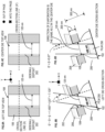
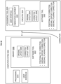
- FIG. 1 depicts a perspective view of fabricating Josephson junctions (JJs) according to embodiments of the present invention.
- JJs Josephson junctions
- FIG. 1 depicts a perspective view of fabricating Josephson junctions (JJs) according to embodiments of the present invention.
- three lithographic patterns/features 108 are shown in FIG. 1 , and each lithographic feature 108 results in a die 120 (e.g., left die 120, center die 120, and right die 120).
- a die 120 may also be referred to as a chip 120.
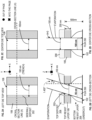
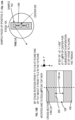
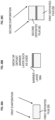
- FIG. 2A is a top view of the left die according to embodiments of the present invention.
- FIG. 2B is a cross-sectional view of the left die according to embodiments of the present invention.
- FIG. 2C is a top view of the center die according to embodiments of the present invention.
- FIG. 2D is a cross-sectional view of the center die according to embodiments of the present invention.
- a resist layer 106 is deposited on a substrate 102.
- the resist layer 106 can be a single or bilayer resist, can include one or more underlayers, such as an anti-reflective coating (ARC), a planarizing layer, or hardmask materials, or can be another stack including a resist, as understood by one skilled in the art.
- ARC anti-reflective coating
- a bottom resist layer 206 is deposited on the substrate 102, and the top resist layer 106 is formed on the bottom resist layer 206.
- the resist layer 106 is patterned in an exemplary shape of the lithographic feature 108, and for explanation purposes, the shape of 108 is a trench.
- the resist layer 106 can be patterned with a lithographic feature 108, for example, to have a Manhattan crossing of trenches that expose the substrate 102 as understood by one skilled in the art.
- the substrate 102 can be a wafer on a wafer stage 104, and the wafer stage holds and moves the wafer 102 substrate during the fabrication as understood by one skilled in the art.
- the terms sample and wafer are used interchangeably.
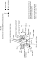
- An evaporation source 150 is used to deposit a film layer 250, such as a superconducting metal.
- the sample 102 and source 150 are tilted relative to each other. This is usually accomplished by tilting the sample stage 104 while keeping the source 150 fixed.
- the sample 102 is also aligned relative to the stage 104 so that the evaporation can occur along an opening in the resist 106 and 206, usually along the long direction of the trench.
- the typical distance L between the source 150 and sample 102 is (relatively) long, e.g., 1 meter (m) (called “throw”).
- the typical resist is a bilayer.
- the thickness of the bottom resist layer 206 used for undercut can be about 300 nm in the z-axes and the thickness of the top resist layer 106 can be about 200 nm.
- the total bilayer resist thickness can be about 500 nm.
- the 1.455° sideway evaporation will displace the pattern by 500 nm ⁇ Tan(1.455°) ⁇ 13 nm from the right resist edge of FIG. 2B , by 300 nm ⁇ Tan(1.455°) ⁇ 8 nm from the left resist edge of FIG.
- the shrinking of the trench opening in the left and right features 108 increases linearly with distance to the center for larger samples (as long as r «L).
- the feature width of film 250 is reduced from 100 nm in the center die 120 as shown in FIG.
- the superconducting material is deposited on top of the top resist layer 106 as a top deposit layer 208, deposited on the side of the top resist layer 106 as a sidewall deposit 202, and deposited in the opening of the top and bottom resist layers 106 and 206 as film layer 250 with width of 95 nm (as depicted in FIG. 2B ).
- the film layer 250 has a full width of 100 nm, as depicted in FIG. 2D .
- the downward arrows represent evaporation (i.e., deposition) of the superconducting material from the evaporation source 150.
- top deposit 208 is shown in top views of FIGS. 2A, 2C , 3A, 3C , 5A, 5C , 7A, 7C , 8A, 8C , 9A , 10A , 11A, 11B , 11C, 11D , 12A, 12B , 12C , 13A, 13B, 13C , 13D , 14A , 14B , 16A , 17A , and 18A .
- Non-limiting examples of suitable materials for the substrate 108 include Si (silicon), strained Si, high-resistivity Si, float-zone Si, SiC (silicon carbide), Ge (germanium), SiGe (silicon germanium), SiGeC (silicon-germanium-carbon), Si alloys, Ge alloys, III-V materials, Al 2 O 3 (sapphire, corundum), SiO 2 (quartz), etc.
- the pattern in the resist layers 106 and 206 can be achieved by lithographic patterning which is followed by development of the resist layers 106 and 206.
- the patterning of the trenches can be by photolithographic patterning which patterns the resist 106, 206 on the substrate 102, and the development process can be, for example, with a tetramethylammonium hydroxide (TMAH) or solvent developer. Additional developers are generally known in the art.
- the pattern of trenches in the resist layers 106 and 206 can alternatively be performed by lithographic patterning and followed by an etching.
- the patterning of the trenches can be by photolithographic patterning that exposes portions of the resist 106 and 206 on the substrate 102, and the etching process can be, for example, a wet or reactive ion etching process that removes exposed portions of the resist 106 and 206 in order to form desired patterns discussed herein.
- junctions in embodiments of the invention can be made with a single step of lithography. By not having multiple steps of lithography, embodiments of the present invention do not need to remove the resist or perform lift off in between evaporation steps, and then spin resist again and expose another lithographic pattern. Rather, embodiments of the present invention are specifically designed to be used with a single patterning step and multiple evaporations/oxidations done without breaking vacuum in the same evaporator. At least 2 types of corrections to be described further can be implemented for a single shadow mask lithographic step. Additionally, it should be understood that any material on top of the resist layers 106 and 206 will eventually be lifted off when the resist layer 106 and 206 are removed except where noted otherwise.
- lift off is a way to finish the device. Lift off can be performed by using a solvent, such as Dow ® Microposit TM Remover or acetone, to remove the resist layer at the end, along with any materials that are attached to the resist but nothing else.
- a solvent such as Dow ® Microposit TM Remover or acetone
- a photoresist is a light-sensitive material.
- a positive resist is a type of photoresist in which the portion of the photoresist that is exposed to light becomes soluble to the photoresist developer. The unexposed portion of the photoresist remains insoluble to the photoresist developer.
- a negative photoresist is a type of photoresist in which the portion of the photoresist that is exposed to light becomes insoluble to the photoresist developer. The unexposed portion of the photoresist is dissolved by the photoresist developer.
- embodiments of the present invention can utilize electron-beam lithography (often abbreviated as e-beam lithography) which is the practice of scanning a focused beam of electrons to draw custom shapes (i.e., exposing) on a surface covered with an electron-beam-sensitive film called an electron-beam (or e-beam) resist.
- the electron beam changes the solubility of the electron-beam resist, enabling selective removal of either the exposed or non-exposed regions of the resist by immersing it in a developer (e.g., a specific solvent).
- the purpose, as with photolithography is to create very small structures in the resist that can subsequently be transferred to the substrate material, often by etching or deposition.
- Non-limiting examples of suitable electron-beam resists include Poly(methyl methacrylate) (PMMA), which is a type of positive electron-beam resist, and Hydrogen silsesquioxane (HSQ), which is a type of negative electron-beam resist.
- PMMA Poly(methyl methacrylate)
- HSQ Hydrogen silsesquioxane
- a positive electron-beam resist is a type of resist in which the portion of the resist that is exposed to the electron beam (as opposed to light) becomes soluble to the electron-beam resist developer. The unexposed portion of the electron-beam resist remains insoluble to the electron-beam resist developer.
- a negative electron-beam resist is a type of resist in which the portion of the resist that is exposed to the electron beam (as opposed to light) becomes insoluble to the electron-beam resist developer.
- the unexposed portion of the electron-beam resist is dissolved by the electron-beam resist developer.
- Other methods for performing e-beam lithography for example but not limited to using lift off resist (LOR) or electron-beam resist bilayers, are understood by one skilled in the art.
- corrections are discussed herein. For combinations of multiple corrections, one can build a more specific model. There can be other corrections that are within the scope of the present invention, solely defined by the claims, but not explicitly discussed.
- Custom correction models can be built using the ideas presented.
- area correction methods for shadow evaporations and designers apply it specifically to Josephson junctions used in quantum computing, where the critical current (I c ) of the junction is sensitive to the area (and oxide or barrier thickness) of the junction.
- the discussed corrections specify the pattern/dose adjustments needed to achieve the desired feature size/area. This can be implemented in a way that does not necessarily preserve the exact (original) position/coordinates of the structure (within a die). Alternatively and additionally, it can also be implemented in a particular way that does preserve the feature coordinates (also within a die, optional).
- Automated corrections can be implemented at the post processing or fracture stage, either in house (e.g., at mask design shops) or in commercial packages, such as CATS or Beamer.
- the corrections are categorized into the following non-limiting categories:
- Positional tilt corrections discussed herein address corrections along the x or y axis, and any combination thereof can be a vector decomposed into these 2 component corrections (i.e., x and y axes).
- a single sidewall deposit correction requires 2 evaporation steps. Multiple sidewall deposit corrections (for 3 or more evaporation steps) in the same trench could require detailed considerations in accordance with embodiments of the present invention, by which a custom model can be generated.
- Flashing corrections could require a detailed quantitative understanding of the developed resist profile for the particular process. Possible solutions/corrections include: increasing the available undercut such that flashing does not (or only minimally) occur by undercut engineering, and/or locally correcting the pattern or dose (as discussed in positional corrections) to compensate for reduced feature size due to sidewall flashing.
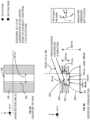
- Test case 1A is depicted as FIGS. 1 , 2A, 2B, 2C, and 2D , and can be corrected using pattern and dose corrections.
- the designers correct the pattern exposed on the left such that the developed channel becomes wider and the evaporation on this left die results in 100 nm film width as depicted in FIGS. 3A, 3B, 3C, and 3D .
- the positional tilt angle ⁇ Tan -1 (r/L), where r is the distance between the evaporation target on the sample and the stage center, and L is the distance between the stage center and the evaporation source.
- the positional tilt angle ⁇ 1.455°.
- ⁇ 0 at the center of the stage 104 (which is the center of the wafer 102).
- the left die 120 i.e., left lithographic feature
- the left die 120 has positional tilt because the left die 120 is not positioned at the center of the wafer 102/stage 104, and the evaporation source 150 is aligned directly to the center of the wafer 102/stage 104.
- the trench is 100 nm wide and a film is to be deposited on the substrate 102 with a 100 nm width just like the center die in FIG.
- shadow mask evaporation by the evaporation source 150 results in a sidewall deposit 202 which reduces the width of trench (in the x-axis) such that the depositing superconducting film 250 has a width of 95 nm in the left die in FIG. 2B instead of the desired 100 nm width (of film 250) in the center die in FIG. 2D .
- This type of problem is referred to as positional tilt, which is corrected with a positional tilt width correction w pos (to be added to the desired total width) in accordance with embodiments in the invention.
- Positional tilt can be corrected for by using pattern corrections and dose corrections.
- a software tool 2002 (having the logic and algorithms) in FIG. 20 is configured to make each of the corrections in integrated circuit mask layout, lithographic equipment, and shadow mask equipment, in accordance with embodiments of the invention.
- Integrated circuit layout also known IC layout, IC mask layout, or mask design, is the representation of an integrated circuit in terms of planar geometric shapes which correspond to the patterns of metal, oxide, semiconductor layers, superconducting layers, etc., that make up the components of the integrated circuit.
- First Solution 1A For pattern corrections, with respect to the pattern feature size of the lithographic feature 108 (i.e., the trench), the designers widen the resist opening (i.e., widen the trench) on the left die only to result in 100 nm width of the film 250 in FIG. 3B by local design modification in the layout (e.g., layout 2004) (which can be performed by software tool 2002).
- the software tool 2002 can be configured to implement a single unique solution for each die on the wafer 102, and smaller corrections can be introduced within a die. According to embodiments of the present invention, this solution can be implemented manually by the designer in the layout 2004 (which may or may not utilize software tools 2002) and/or the solution can be implemented by a software algorithm of the software tool 2002 after layout 2004 of the desired pattern has been designed. Additionally, the solution can be implemented instead by the lithographic patterning tool 2020 depicted in FIG. 20 .
- the lithographic patterning tool 2020 is lithographic equipment that forms a feature or pattern in one or more layers, as understood by one skilled in the art.
- the lithographic patterning tool 2020 could be integrated with, include, and/or be instructed by the software tool 2002.
- Second Solution 1A For pattern dose corrections, a larger exposure dose results in a wider feature for positive tone resists (while a smaller exposure dose results in a wider feature for negative tone resists).
- the pattern dose as can be done for e-beam lithography or a stepper/scanner
- the feature width of feature 108 can be changed to the corrected size (i.e., the trench is changed to be 105 nm wide for the left die (and right die)). This can be accomplished using the software tool 2002 which can be connected to and/or integrated with the fabrication equipment for e-beam lithography and/or a stepper/scanner.
- This solution can utilize the same pattern design (which is the original layout 2004 of the lithographic features 108 in the layers 106, 206, 102) and same mask for the original layout of the lithographic features, but requires a local dose adjustment.
- a local dose adjustment means that each die 120 (each feature 108) can receive a different amount of exposure based on the die's distance from the center in order to create a larger width for the trench (i.e., lithographic feature 108). Smaller corrections can be introduced within a die (for e-beam and other direct write lithography).
- the solution can be implemented by a software algorithm (in the software tool 2002) after layout (a representation of the design).
- the solution can be implemented instead by the lithographic patterning tool 2020, which can be instructed by, for example, the software tool 2002, and/or the software tool 2002 can be integrated with the lithographic patterning tool.
- the conversion factor from dose change (i.e., the amount of exposure) to feature size change needs to be calibrated for a specific tool (e.g., for e-beam lithography) and resist stack (the type of resist layers 106 and 206 and developer being utilized), which is understood by one skilled in the art without undue experimentation in light of the teachings of embodiments of the present invention.
- the feature 108 (such as the trench) is patterned in the resist layer 106 and 206 to have the desired width in the x-axis.
- This expression is a geometrical consequence of the top layer 106 being engineered to be wider than bottom resist layer 206, therefore defining the effective opening of resist (in the absence of previous sidewall deposits or flashing, as will be discussed).
- the total tilt on the left die will be the y tilt +/positional tilt, accordingly, though the exact value of the positional tilt angle may change (especially for large stage tilt angles), as detailed below; if stage 104 is tilted about the y-axis from x to z in the xz plane, the positional tilt ⁇ is to be added to the stage tilt ⁇ , as shown in FIG. 6 . However, if stage 104 is tilted in the y-axis from z to x in the xz plane instead, the positional tilt ⁇ is to be subtracted from the stage tilt ⁇ . It is noted that x and y directions are arbitrary in the figures.
- the evaporation direction can be along the x direction, for example (perpendicular to the feature).
- the axes shown represent a right-handed Cartesian coordinate system. The total tilt varies continuously across a wafer 102. Discretization of correction is arbitrary and only limited by software and error tolerances for a given application. Correction can vary along a same feature (street or avenue) if necessary (such as if the feature is very long, for example, and the error tolerance requires it).
- stage tilt or positional tilt only matters for the purpose of area correction of the overlap between two deposited films if the area of the overlap is modulated by either type of tilt.
- the generalized positional tilt becomes independent of the stage tilt for trenches 108 that are parallel to the yz plane. This statement is true as long as the tip of the trenches 108 do not determine the overlap area (i.e., the overlap area is determined by a crossing away from the tips of the features such as trenches 108).
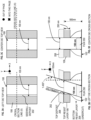
- Test case 1B is depicted in FIGS. 4 , 5A, 5B, 5C, and 5D , and can be corrected analogously using pattern and dose corrections as discussed above in test case 1A.
- the designers correct the pattern exposed on the top die such that the developed channel becomes wider in the y-axis and the evaporation on this top die results in a 100 nm film width (not shown but analogous to FIGS. 3A, 3B, 3C, and 3D ).
- the test case 1B in FIG. 4 is the same as test case 1A except the stage 104 is rotated 90° relative to test case 1A. This means that the parameters and layers are the same in both FIG. 1 and in FIG. 4.
- FIG. 4 depicts lithographic patterns/features 108, and each lithographic pattern 108 results in a die 120 (e.g., top die 120, center die 120, and bottom die 120).
- FIG. 5A is a top view of the top die according to embodiments of the present invention.
- FIG. 5B is a cross-sectional view of the top die according to embodiments of the present invention.
- FIG. 5C is a top view of the center die according to embodiments of the present invention.
- FIG. 5D is a cross-sectional view of the center die according to embodiments of the present invention.
- the width instead of the width increasing in the x-axis as depicted in FIGS. 3A and 3B , the width will increase in the y-axis with respect to FIGS. 4 , 5A, 5B because of the narrower projection of the deposited film through the opening of the top resist layer 106.
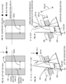
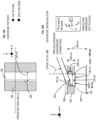
- Test case 1C is depicted as FIGS. 6 , 7A, 7B, 7C, and 7D , and can be corrected using pattern and dose corrections as discussed above.
- the designers correct the pattern exposed on both the left and center dies such that the developed channel becomes wider and the evaporation on the left and center dies each result in 100 nm film width as depicted in FIGS. 8A, 8B, 8C, and 8D .
- FIG. 6 depicts a perspective view of fabricating Josephson junctions according to embodiments of the present invention.
- FIG. 6 is similar to FIGS. 1 and 4 except for different angles.
- FIG. 7A depicts a top view of the left die in FIG. 6 according to embodiments of the present invention.
- FIG. 7B depicts a cross-sectional view of the left die in FIG. 7A according to embodiments of the present invention.
- FIG. 7C depicts a top view of the center die in FIG. 6 according to embodiments of the present invention.
- FIG. 7D depicts a cross-sectional view of the center die in FIG. 7C according to embodiments of the present invention.
- Test case 1C addresses stage tilt of the stage 104.
- stage tilt there are two sets of axes.
- the state tilt ⁇ is about the y-axis from the x-axis to the z-axis in the xz plane.
- the stage tilt ⁇ 5.67°.
- the generalized positional tilt may not vary significantly with stage tilt, such that ⁇ ⁇ ⁇ as long as the stage tilt ⁇ is reasonably small and the distance r on the wafer to its center is much smaller than the distance L to the evaporation source.
- FIGS. 8A, 8B, 8C, and 8D depict the lithographic pattern/feature 108 with a wider pattern.
- FIG. 8A is a top view of the left die according to embodiments of the present invention.
- FIG. 8B is a cross-sectional view of the left die according to embodiments of the present invention.
- FIG. 8C is a top view of the center die according to embodiments of the present invention.
- FIG. 8D is a cross-sectional view of the center die according to embodiments of the present invention.
- the designers can design a wider trench at each location of the die 120 (first solution 1A) and/or expose (the resist) with a larger dose at each location of the die 120 (second solution 1A).
- a larger dose can be with a greater beam intensity (i.e., increased magnitude) and/or longer exposure time (as compared to what is needed if the positional corrections were not being made), and this causes a wider trench pattern in the top resist 106.
- t top is the nominal thickness of the top resist layer
- ⁇ ' ⁇ + ⁇ ⁇ ⁇ + ⁇ is the total tilt.
- FIG. 7B shows the film 250 with a width of 75 nm in the x'-axis when a 100 nm width was originally designed and FIG. 7B shows the deposited film 250 with a width of 80 nm in the x'-axis when a 100 nm width was originally designed.
- the solutions implemented by the designers have corrected for both the positional tilt ⁇ and the stage tilt ⁇ .
- JJ Josephson junction
- Two trenches 108 made into resist are separated by a small resist gap along the y axis such as in FIG. 1 . Both trenches are aligned with each other in their long dimensions along the y axis.
- the resist gap may be 200 nm.
- the resist gap contains only top resist layer 106 and no bottom resist layer 206, and this resist gap is supported on two opposite sides in the x axis by top resist layer 106 which contains bottom resist layer 206 under it.
- the resist gap with suspended top resist is known as a Dolan bridge.
- Second film 250 will then deposit towards the bottom trench and under the Dolan bridge.
- the respective thicknesses of the top and bottom resist layers may be designed to allow the oxidized first film 250 to overlap with the second film 250, creating a tunnel junction.
- the sidewall deposit correction is to correct a channel (e.g., trench) that contains a sidewall deposit from a previous shadow evaporation in order to result in a desired 100 nm film width for the deposited film 250 in this example.
- a channel e.g., trench
- Manhattan junction fabrication by shadow evaporation is a non-limiting example where sidewall deposit correction is important.
- FIGS. 1 and 4 shows perspective views of the source evaporator 150 relative to the wafer 102/stage 104, and these views are not repeated but can be referenced herein.
- Test case 2A is depicted in FIGS. 9A and 9B
- the solution is depicted in FIGS. 10A and 10B .
- Solution 2A (to test case 2A) is to calculate how much street width (e.g., the width of the trench) was reduced by the expected width of sidewall deposit from previous evaporation(s) that generate the sidewall deposits.
- the sidewall width correction w side ⁇ i [t nom,i x Sin( ⁇ ' i )], where t nom,i is the nominal thickness of previous evaporation of index i which landed on the sidewall, ⁇ ' i is the total tilt angle relative to the vertical z direction of the evaporation of index i used to create the respective sidewall deposit of index i, and ⁇ i is the sign for summation over all indices i (in which an evaporation landed on the sidewall).
- the nominal thickness of an evaporation is a calibrated value which is tracked in real time by a device such as a crystal monitor mounted in the vacuum chamber within an evaporator. It corresponds to the thickness of a given material when deposited onto a flat surface without stage tilt.
- the designers increase the street width by the amount of sidewall width reduction, either by using pattern or dose corrections.
- This correction can be in addition to applicable tilt (both positional tilt and stage tilt) corrections (test case 1A, 1B, and 1C), but multiple such corrections are additive to first approximation.
- the geometry of each sidewall profile and how each deposit attaches to the sidewall must be taken into account in the model used to apply the corrections.
- the need for a sidewall correction depends on how the subsequent evaporation affects the overlap area between the two or more films.
- the total width correction w tot is the result of the addition of the sidewall width correction w side (resulting from previous evaporations) with other types of correction for the subsequent evaporation, such as the positional tilt width correction w pos (or flashing width correction w flash ), with minor modifications.
- the total width correction w tot w side + t eff x Tan( ⁇ '), where t eff is the effective thickness of the top layer (modified by the sidewall deposit(s)), and ⁇ ' is the total tilt angle relative to the vertical z direction.
- the effective thickness of the top layer is not equal the top resist layer.
- the effective thickness depends on the angle of the sidewall deposit evaporation(s), height(s), history of sidewall attachment, and direction of the new evaporation.
- FIG. 9A depicts a top view of the center die according to embodiments of the present invention.
- FIG. 9B depicts a cross-sectional view of the center die according to embodiments of the present invention.
- evaporation material is not shown on the top, so as not to obscure the figure. The parameters are changed from above.
- FIG. 9A evaporation material is not shown on the top, so as not to obscure the figure. The parameters are changed from above.
- the thickness of the top resist layer 106 in the z'-axis is 250 nm and the thickness of the bottom resist layer 206 in the z'-axis is 250 nm.
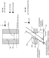
- a previous shadow evaporation (1 st shadow evaporation) resulted in the sidewall deposit 202 with a nominal thickness of 40 nm in the direction of evaporation as defined along the original z-axis. Because of the previous shadow evaporation, the width of the trench opening (i.e., feature 108) is reduced from 100 nm to 80 nm.
- the nominal thickness of the previous shadow evaporation (1 st evaporation) is 40 nm in the evaporation direction (z direction) and performed at a 30° evaporation angle relative to the vertical z direction as shown in FIGS. 9B and 10B .
- the previous shadow evaporation leaves no film 250 deposited on sample 102 inside trench 108.
- the previous shadow evaporation leaves film 250 deposited inside trenches 108 that are not shown and are at a right angle with the trenches 108 that are shown.
- the designers For building a Manhattan junction, the designers must rotate the stage 90° in the xy plane and next evaporate parallel to the trench (i.e., shadow evaporation is along the y-axis), resulting in an overlap of films 250 along trenches 108 that are shown and right angle trenches 108 that are now shown, at the intersections of the two types of trenches. Because there is no positional tilt in the center die, and the next evaporation is performed parallel to the trench 108, there is only a sidewall correction to be applied as a consequence of the sidewall deposit 202 shown in FIGS. 9A and 9B . The designers increase the width of the trench by 20 nm to get 100 nm deposited film 250 (not shown) into the trench in the center in the 2 nd evaporation. This can be achieved with design or dose correction as discussed above.
- the trench opening is 100 nm before the 1 st shadow evaporation but will result in an 80 nm deposited film after the 1 st shadow evaporation in FIG. 9B .
- FIG. 10A is a top view of the center die according to embodiments of the present invention.
- FIG. 10B is a cross-sectional view of the center die according to embodiments of the present invention.
- the trench (feature 108) is corrected to have a trench width of 120 nm in the x'-axis instead of 100 nm (in FIGS. 9A and 9B ), and this results in a deposited film (from a subsequent evaporation along the y axis, like layer 250 but not shown) with width 100 nm in FIG. 10B instead of 80 nm which as in FIG. 9B .
- Test case 2B is depicted in FIGS. 11A, 11B, 11C, 11D , 12A, 12B , and 12C .
- FIG. 11A is a simplified top view of the stage 104 holding the sample 102, without showing the evaporation source 150 although it is understood that the evaporation source is present.
- stage tilt ⁇ 1 30° of first evaporation
- stage tilt ⁇ 1 30° of first evaporation
- the thickness (which is 40 nm in the example scenario) utilized in the calculation is the nominal thickness of the sidewall deposit 202 at the angle of evaporation that created the sidewall deposit 202.
- Calculating 21 nm for the sidewall width correction w side means that the opening of the trench (feature 108) would need to be 121 nm (which is an additional 21 nm) in order to deposit a film 250 (not shown) with a width of 100 nm for an evaporation directly along the trench (otherwise there will be a new positional tilt as will be described next).
- a Manhattan crossing there will be another trench 108 (not shown) which intersects the trench 108 of FIG.
- FIG. 11C is a simplified top view of the stage 104 in FIG. 11A with a 90° rotation of the stage 104 about the z-axis from y to x in the xy plane.
- FIG. 11D is a top view of the top die shown in FIG. 11C . After the 90° rotation of the stage 104 about the z-axis from y to x in the xy plane, the left die of FIG. 11A becomes the top die of FIG. 11C .
- FIG. 12A is a simplified top view of the stage 104 holding the wafer 102 as in FIG. 11C .
- FIG. 12B is a top view of the rotated and tilted left die of FIG. 11A , as shown by the tilted axes (y'and z').
- FIG. 12C is a cross-sectional view of the rotated and tilted left die of FIG. 11A .
- the subsequent stage tilt of 35° for the subsequent evaporation has no effect on the generalized positional tilt because it is performed along the trench 108 of FIG. 12B .
- An overlay is created with the first film deposited during the first evaporation into the another trench 108 which intersects the trench 108 of FIG. 12B at a right angle (the another trench 108 is not shown).
- This overlay is a Manhattan crossing, the overlay area of which will require both a sidewall correction and a positional tilt correction.
- the effective opening of the trench (feature 108) at the top t eff for an evaporation of a film 250 landing on the sample 102 in the space under the sidewall deposit 202 depends on the lower edge (i.e., anchoring point) of the previous sidewall deposit 202 on the right and the top edge of the top resist layer 106 on the left.
- the widening of the trench in the left die of FIG. 11B (which was rotated by 90° after the first evaporation about the z-axis from y to x in the xy plane) for the purpose of correcting the width of the deposited film can be accomplished with pattern design or dose as discussed above.
- Test case 2C is depicted in FIGS. 13A, 13B, 13C, 13D , 14A, 14B , and 14C .
- FIG. 13A is a simplified top view of the stage 104 holding the wafer 102, without showing the evaporation source 150 although it is understood that the evaporation source is present.
- positional tilt ⁇ 1 1.455° of first evaporation
- stage tilt ⁇ 1 30° of first evaporation
- stage tilt ⁇ 1 30° of first evaporation
- the thickness (which is 40 nm in the example scenario) utilized in the calculation is the nominal thickness of the sidewall deposit 202 at the angle of evaporation that created the sidewall deposit 202.
- Calculating 19 nm for the sidewall width correction w side means that the opening of the trench (feature 108) would need to be 119 nm (which is an additional 19 nm) in order to deposit a film 250 (not shown) with a width of 100 nm for an evaporation directly along the trench (otherwise there will be a new positional tilt as will be described next).
- FIG. 13C is a simplified top view of the stage 104 in FIG. 13A with a 90° rotation of the stage 104 about the z-axis from y to x in the xy plane
- FIG. 13D is a top view of the bottom die shown in FIG. 13C .
- the right die of FIG. 13A becomes the bottom die of FIG. 13C .
- FIG. 14A is a simplified top view of the stage 104 holding the wafer 102 as in FIG. 13C .
- FIG. 14B is a top view of the rotated and tilted right die of FIG. 13A , as shown by the tilted axes (y'and z').
- FIG. 14C is a cross-sectional view of the rotated and tilted right die of FIG. 13A .
- the subsequent stage tilt of 35° for the subsequent evaporation has no effect on the generalized positional tilt because the evaporation is performed along the trench 108 of FIG. 14B .
- An overlay is created with the first film deposited during the first evaporation into the another trench 108 which intersects the trench 108 of FIG. 12B at a right angle (the another trench 108 is not shown).
- the difference between cases 2B and 2C relies on the position of the die relative to the center only, while all stage tilts, rotation angles, and evaporated thicknesses remain the same.
- the effective opening of the trench (feature 108) at the top t eff for an evaporation of a film 250 landing on the sample 102 in the space that is not under the sidewall deposit 202 now depends on the top edge of the previous sidewall deposit 202 on the right and the bottom edge of the top resist layer 106 on the left.
- the widening of the trench in the left die of FIG. 13B (which was rotated by 90° after the first evaporation about the z-axis from y to x in the xy plane) for the purpose of correcting the width of the deposited film can be accomplished with pattern design or dose as discussed above.
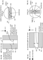
- Test case 3 is depicted in FIGS. 15 , 16A , and 16B .
- FIG. 15 depicts a view of the stage 104 and evaporation source 150 as discussed herein.
- FIG. 16A depicts a top view of the left die 120.
- FIG. 16B depicts a cross-sectional view of the left die in FIG. 16A .
- An evaporation is projected far enough to the side (due to small resist undercut, high tilt, and/or both) that the deposited film 250 partly (and unintentionally) ends upon the undercut sidewall of the bottom resist 206 instead of the substrate 102, which (further) reduces the width of the evaporated feature (i.e., film 250) on the substrate 102.
- First Solution 3 is undercut engineering.
- Undercut engineering is configured to add/extend sublithographic shapes or partial dose features next to the channel (i.e., trench opening) in order to increase the width of the undercut.
- the undercut is the curved sidewall of the bottom resist layer 206, which is cut/removed under the top resist layer 106. If the undercut (of bottom resist layer 206) increases sufficiently, the deposited features (i.e., film 250) no longer end up on the undercut sidewall. This can be done quantitatively for specific features and locations, but the undercut can also be increased preventively without quantitative analysis. There is a practical limit to the extent of increasing the undercut.
- Second Solution 3 is the following.
- the reduced feature width (film 250) due to sidewall flashing can also be corrected by increasing the channel width (i.e., the opening of the trench feature 108) by the correction amount w flash .
- a predictive calculation requires detailed quantitative knowledge of the resist profile, particularly the resist thicknesses and the amount of undercut. Additionally, the needed correction can also be determined empirically.
- the channel width increase can be achieved by pattern or dose correction.
- FIG. 16B the deposited film 250 abuts and lands (i.e., flashes) on the curved sidewall of the bottom resist layer 206. Flashing on the curved sidewall reduces the width of the film 250 in the x'-axis (axes are assumed to be tilted by some arbitrary value, in accordance to previous configurations of the correction to be performed).
- FIG. 17A depicts a top view of the left die
- FIG. 17B depicts a cross-sectional view of FIG. 17A .
- the left side of the undercut of resist 206 is increased, which prevents the film 250 from landing on the curved sidewall of the bottom resist 206 and allows the entire film 250 to be deposited on the substrate 102. This is the first solution 3.
- FIG. 18A depicts a top view of the left die
- FIG. 18B depicts a cross-sectional view of FIG. 18A
- the width of the trench feature 108 is increased to compensate for the sidewall deposit 202.
- the deposited film 250 can still hit or land on the curved sidewall of the bottom resist 206, but the film 250 has the correct width in the x'-axis because of the increased trench width (opening) in the x'-axis.
- FIG. 19 depicts a cross-sectional view as examples of 3 completed Josephson junctions 1902 using the one or a combination of any of the shadow evaporation corrections discussed herein according to embodiments of the present invention.
- 2 shadow evaporations are required.
- the first shadow evaporation deposits the first film 250 on the substrate 102. Corrections, such as positional tilt corrections and/or sidewall flashing corrections, have been applied to the first shadow evaporation. There is no need for sidewall corrections to be applied to the first shadow evaporation from the evaporation source 150 because no sidewall deposit 202 has occurred prior to the first shadow evaporation.
- an oxide layer 1904 is grown on top of first film 250.
- the superconducting metal of the first film 250 can be oxidized to form the oxide layer 1904.
- the oxide is typically grown by oxidizing the existing superconductor metal, such as Aluminum, without breaking vacuum. This is done by introducing oxygen gas into the evaporation chamber or an attached oxidation chamber that the sample can be transferred to and from without vacuum break at this step.
- an oxide can be deposited instead of grown.
- shadow evaporation was discussed to deposit a film only on the substrate 102 for explanation purposes. It is understood to form a Josephson junction that the second film is deposited on the previously deposited film (particularly on the oxide layer), thereby resulting in a Josephson junction.
- a second shadow evaporation from the evaporation source 150 is performed to deposit the second film 250 on top of the oxide layer 1904.
- the second shadow evaporation has been corrected for corrections, such as positional tilt corrections, sidewall flashing corrections, and/or sidewall deposit corrections. It is noted that sidewall deposit corrections are accounted for only after a previous shadow mask evaporation has occurred (e.g., the first shadow mask evaporation).
- the bottom resist layer 206, top resist layer 106, and any deposited material from shadow evaporations (such as the sidewall deposit 202 and top deposit 208) formed on the top resist layer 106 are removed. This leaves the 3 Josephson junctions 1902 on the substrate 102.
- FIG. 20 depicts example systems configured to perform the corrections discussed herein according to embodiments of the present invention.
- a computer system 2000 includes a software tool 2002 configured with one or more algorithms to perform positional tilt corrections, sidewall deposit corrections, and/or sidewall flashing corrections for design features 108 in an original layout 2004, in order to generate a corrected layout 2006.
- the software tool 2002 can include the functionality to allow for layout 2004 of a design that is to be fabricated and/or can receive loading of the original layout 2004 in order to perform the corrections discussed herein.
- the computer system 2000 includes one or more processors 2010 configured to execute instructions of the software tool 2002, thereby generating the corrected layout 2006 from the original layout 2004.
- the computer system 2000 can transmit the corrected layout 2006 to a lithographic tool 2020.
- the lithographic tool 2020 can include the software tool 2002 and/or functionality of the software tool 2002 such that the lithographic tool 2020 is configured to make the corrections to the original layout 2004 to generate the corrected layout 2004.
- the lithographic tool 2020 includes fabrication equipment 2022 for fabricating semiconductor circuits (including superconducting circuits) as understood by one skilled in the art.
- the fabrication equipment 2022 can represent a variety of fabrication devices which can be separate or integrated in a fabrication lab.
- the lithographic tool 2020 includes the circuitry 2024 (hardware along with software) to operate as discussed herein.
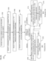
- the lithographic tool 2020 alone and/or in conjunction with the computer system 2000 is configured to perform a process in FIGS. 27A and 27B .
- FIGS. 27A and 27B depict a flow chart 2700 of a process for correcting and forming Josephson junctions for superconducting qubits when depositing the films 250 of the Josephson junction using sequential shadow mask evaporations.
- the software tool 2002 receives the choice of critical current Ic values for Josephson junctions in superconducting qubits to be fabricated.
- the software tool 2002 receives selection of the Josephson junction design/style (e.g., Dolan bridge Josephson junctions, Manhattan Josephson junctions, other shadow-masked Josephson junctions).
- the software tool 2002 receives selection of the fabrication process and parameters (e.g., tilt angles for shadow evaporations, oxidation conditions).
- the design/style for Dolan bridge Josephson junctions and Manhattan Josephson junctions have fabrication process and parameters for height/thickness/multilayer/undercuts, bridge dimensions, tilt angles, rotation angles, film thicknesses, sample size, etc., as understood by one skilled in the art.
- the software tool 2002 (which can include the features of a state-of-the-art layout tool) designs the Josephson junctions that nominally confirm with the style and fabrication parameters, thereby creating the original layout 2004.
- the originally layout 2004 is a file (i.e., computer file).
- original layout 2004 can be created by a state-of-the-art software program, and then loaded to the computer system 2000 for corrections.
- the corrections discussed herein can be manual or automatic corrections.
- the software tool 2002 is configured to apply software automated corrections at wafer and die level to the original layout (design) 2004 for the type of Josephson junctions and shadow mask recipe. This creates the corrected layout (design) 2006.
- Corrected layout 2006 can be a separate layout in one implementation, and the corrected layout 2006 can be an updated version of the original layout 2004.
- a layout is a representation of a design, and often used interchangeably.
- the software (or manual) correction will take each of the features 108 in the design and adjust these features 108 to achieve the desired effect (i.e., positional tilt correction, sidewall deposit correction, sidewall flashing correction) either at the individual die level (die is a unit of repetition of a mask design on a wafer), or wafer level (that is, corrects features on separate dies differently).
- the layout becomes a file that can be used for lithography.
- the software tool 2002 is configured to check if there are any further design corrections that the operator desires to manually make.
- the software tool 2002 is configured to display a message asking the operator if he wants to make further manual corrections addressing positional tilt correction, sidewall deposit correction, and/or sidewall flashing correction.
- the software tool 2002 is configured to apply any remaining lithographic corrections at the die and wafer level with automated software to the lithographic pattern of a sample, for the type of Josephson junctions and shadow mask recipe at block 2716.
- the mask design (i.e., corrected layout file 2006) of the previous block is entered as input to a lithographic tool 2020 such as an e-beam writer (which is a type of fabrication equipment).
- a lithographic tool 2020 such as an e-beam writer (which is a type of fabrication equipment).
- An e-beam writer or a direct write laser lithography system can be particularly utilized for embodiments of the present invention because of the feature size and versatility afforded.
- the fabrication equipment 2022 can also be representative of optical lithography equipment in which an optical mask is a physical object that is fixed in shape and used to pattern the features with light of a fixed wavelength (corresponding to a location in the optical spectrum, e.g., ultraviolet, visible, infrared).
- the operator and or software tool 2002 can additionally provide a job file as input to the lithographic tool 2020, which manages how to handle the design input which is the corrected layout 2006.
- the lithographic tool 2020 (for an e-beam writer, for example) can provide a mechanism (such as software tool 2002) to receive a mask design (original layout 2004) and modify it (to be the corrected layout 2006) for the purpose of area correction in the multiple-shadow-mask fabrication.
- a mechanism such as software tool 2002 to receive a mask design (original layout 2004) and modify it (to be the corrected layout 2006) for the purpose of area correction in the multiple-shadow-mask fabrication.
- the software tool 2002 integrated in the lithographic tool 2020 would post-process the original layout to correct it for that type of fabrication (i.e., e-beam), and the exposures of the pattern on the wafer (or sample) would come out corrected.
- the software can check (e.g., display a message) whether the operator wants to any manual lithographic patterning corrections.
- the lithographic tool 2020 makes the Josephson junctions according to the fabrication process and parameters. Fabricating the Josephson junctions can include depositing the resists 106, 206 on the wafer 102, exposing the resists 106, 206, etching substrate 102, developing the resists 106, 206, performing shadow mask evaporation (i.e., depositing first and second films 250) and oxidation or oxide deposition (for oxide layer 1904) according to the planned shadow mask recipe (i.e., design), and performing lift off of the resists 106, 206 leaving Josephson junctions 1902.
- shadow mask evaporation i.e., depositing first and second films 250
- oxidation or oxide deposition for oxide layer 1904
- a sample analysis can be performed to verify that the corrections occurred as desired. If yes, the sample is ready, the flow branches to block 2724.
- the operator can apply manual corrections at wafer and die level to the original layout (design) 2004 for the type of Josephson junctions and shadow mask recipe. This creates the corrected layout (design) 2006.
- the operator could use the software tool 2002.
- the operator can check if there are further automatic design corrections. If no automatic design corrections needed, the operator can apply any remaining lithographic corrections at the die and wafer level without automated software to the lithographic pattern of a sample, for the type of Josephson junctions and shadow mask recipe at block 2734. The operator can use the software tool 2002.
- the operator can check if further automatic lithographic patterning corrections are needed. If yes the flow branches to 2716, and if no the flow branches to block 2720.
- a wafer/sample 102 would have resist (spun over it) which is sensitive to the patterning tool exposure method (via the lithographic tool 2020). If e-beam is utilized as the fabrication method, the beam is deflected according to the specifications of the mask design and job file (and dose (for e-beam lithography, the dose may be defined as the electric charge per unit area) over areas of the wafer 102 to sensitize the e-beam resist (for example, PMMA or equivalent).
- optical lithography is utilized as the fabrication method, light of a fixed wavelength shines into the apertures of a physical optical mask, and where the mask is transparent, the resist is sensitized (photoresist). Because optical lithography uses a physical mask, it is not possible to make local dose modifications within a single die (for optical lithography, the dose may be defined as the intensity times the exposure time). A die is typically the result of a single exposure through the physical optical mask. But it is possible to modify the dose applied to different dies within the wafer using optical lithography.
- embodiments of the present invention have a bilayer of resist (top resist 106 and bottom resist 206), where an underlayer (bottom resist 206) is used to provide an undercut, as seen in some of the figures (this is a positive tone process).
- the fabrication involves making Josephson Junctions 1902 of a given area (given by the overlap of two evaporations) using shadow-masking, not breaking vacuum, and schemes such as Dolans or Manhattans (or other structures).
- Other methods of fabricating Josephson junctions (or other tunnel junctions) where a point evaporation source is involved may also correct for overlap area using the corrections described here.
- the fabrication of the Josephson junction may result in less variability across a wafer by applying positional or flashing corrections (sidewall corrections can only be applied if there are multiple evaporations prior to stripping the resist (i.e., prior to lift off)).
- the automated software tool 2002 can make the corrections such that the user does not have to make those calculations.
- FIG. 21 a flow chart 2100 is provided of a method for correcting an area of overlap between two films created by sequential shadow mask evaporations according to embodiments of the present invention. Reference can be made to the figures discussed herein.
- an operator performs at least one process selected from the group consisting of: correcting design features 108 in an original layout 2004 to generate a corrected layout 2006 using a software tool 2002, such that the corrected layout 2006 has modified shapes of the design features 108 at block 2104, and/or correcting the design features 108 in the original layout 2004 to generate the corrected layout 2006 using a lithographic tool 2020, such that the corrected layout 2006 has modified shapes of the design features 108 at block 2106.
- the lithography tool 2020 (which can be instructed by the software tool 2002 and/or operator) is configured to pattern the modified shapes of the design features 108 at locations on a wafer 102 according to the corrected layout 2006.
- the lithography tool 2020 is configured to deposit a first film 250 by an initial shadow mask evaporation (as depicted in FIG. 26A ) and a second film 250 (as depicted in FIG. 26C ) by a subsequent shadow mask evaporation to produce corrected junctions (e.g., junction 1902) at the locations on the wafer 102, such that the first and second films 250 have an overlap (as depicted in FIG. 19 ).
- the overlap between the first and second films 250 defines a tunnel junction.
- the overlap between the first and second films 250 defines a Josephson junction (JJ).
- the initial and subsequent shadow mask evaporations may utilize a suspended resist bridge.
- the suspended resist bridge can be formed by the bilayer resist of resist layers 106 and 206.
- the initial and subsequent shadow mask evaporations may utilize a crossing without a suspended resist bridge. The crossing relates to a Manhattan crossing. Corrections (such as positional tilt correction, sidewall deposit correction, and/or sidewall flashing correction) to the original layout 2004 account for (accommodate) narrowing of the design features 108 (e.g., the trench in example scenarios) from previous depositions (by shadow mask evaporation) prior to the subsequent shadow mask evaporation.
- An oxide layer 1904 is between the first film 250 and the second film 250.
- the corrected layout 2006 includes a positional tilt correction.
- the positional tilt correction is configured to modify the shapes (i.e., trench) of the design features 108 relative to a position of an evaporation source 150 and individual ones of the design features 108.
- the corrected layout 2006 includes a sidewall deposit correction.
- the sidewall deposit correction is configured to modify the shapes (e.g., trenches) of the design features 108 relative to a previous sidewall deposit 202 from a previous shadow mask evaporation.
- the corrected layout 2006 includes a sidewall flashing correction.
- the sidewall flashing correction is configured to modify the shapes of the design features 108 to prevent a width of the first film 250, the second film 250, or both the first and second films 250 from being reduced by flashing against a sidewall of a resist material (e.g., the bottom resist layer 206).
- Corrections in the corrected layout include at least two types of corrections selected from the group consisting of: a positional tilt correction, a sidewall deposit correction, and/or a sidewall flashing correction.
- FIG. 22 depicts a flow chart 2200 of a method of forming junctions according to embodiments of the present invention. Reference can be made to the figures discussed herein.
- the operator can utilize the software tool 2002 and/or the lithographic tool 2020 to correct the design features 108 in an original layout 2004 to generate a corrected layout 2006.
- the operator can utilize the lithographic tool 2020 to pattern the design features 108 of the corrected layout 2006 at locations on a wafer 102.
- the lithographic tool 2020 is configured to deposit a first film 250 (as depicted in FIG. 26A ) and a second film 250 (as depicted in FIG. 26C ) using shadow mask evaporation according to the corrected layout 2006, where the corrected layout 2006 corrects for deposition by the shadow mask evaporation.
- An overlap between the first and second films 250 defines a tunnel junction.
- An overlap between the first and second films 250 defines a Josephson junction.
- Correcting the design features in the original layout to generate the corrected layout comprises widening shapes (i.e., widening the trench) of the design features 108 relative (i.e., with respect to angles of evaporation) to an evaporation source.
- the oxide layer 1904 is between the first film and the second film.
- the corrected layout includes a positional tilt correction.
- the corrected layout includes a sidewall deposit correction.
- the corrected layout includes a sidewall flashing correction.
- FIG. 23 depicts a flow chart 2300 for correcting an area of overlap between two films created by sequential shadow mask evaporations according to embodiments of the present invention. Reference can be made to the figures discussed herein.
- software tool 2002 and/or the lithographic tool 2020 is configured to correct design features 108 in an original layout 2004 to generate a corrected layout 2006, where the design features 108 in the corrected layout 2006 have been modified to account in advance for being at different positions relative to an evaporation source 150.
- the lithographic tool 2020 (software tool 2002 can instruct the lithographic tool 2020) is configured to pattern the design features 108 of the corrected layout 2006 at locations on a wafer 102.
- the lithographic tool 2020 (software tool 2002 can instruct the lithographic tool 2020) is configured to deposit a first film 250 (as depicted in FIG. 26A ) and a second film 250 (as depicted in FIG. 26C ) using shadow mask evaporation according to the corrected layout 2006.
- FIG. 24 depicts a flow chart 2400 for correcting an area of overlap between two films created by sequential shadow mask evaporations according to embodiments of the present invention. Reference can be made to the figures discussed herein.
- the software tool 2002 and/or the lithographic tool 2020 is configured to correct design features 108 in an original layout 2004 to generate a corrected layout 2006, where the design features 108 in the corrected layout 2006 have been modified to account in advance for sidewall deposits of material (e.g., sidewall deposit 202) on the design features 108 from an evaporation source 150.
- sidewall deposits of material e.g., sidewall deposit 202
- the lithographic tool 2020 (software tool 2002 can instruct the lithographic tool 2020) is configured to pattern the design features 108 of the corrected layout 2006 at locations on a wafer 102.
- the lithographic tool 2020 (software tool 2002 can instruct the lithographic tool 2020) is configured to deposit a first film 250 (as depicted in FIG. 26A ) and a second film 250 (as depicted in FIG. 26C ) using shadow mask evaporation according to the corrected layout 2006.
- FIG. 25 depicts a flow chart 2500 for correcting an area of overlap between two films created by sequential shadow mask evaporations according to embodiments of the present invention. Reference can be made to the figures discussed herein.
- the software tool 2002 and/or the lithographic tool 2020 is configured to correct design features 108 in an original layout 2004 to generate a corrected layout 2006, where the design features 108 in the corrected layout 2006 have been modified to account in advance for flashing against a sidewall of a resist (e.g., bottom resist layer 206 having the curved undercut) during a shadow mask evaporation.
- a resist e.g., bottom resist layer 206 having the curved undercut
- the lithographic tool 2020 (software tool 2002 can instruct the lithographic tool 2020) is configured to pattern the design features 108 of the corrected layout 2006 at locations on a wafer 102.
- the lithographic tool 2020 (software tool 2002 can instruct the lithographic tool 2020) is configured to deposit a first film 250 (as depicted in FIG. 26A ) and a second film 250 (as depicted in FIG. 26C ) using shadow mask evaporation according to the corrected layout 2006.
- superconducting materials at low temperatures, such as about 10-100 millikelvin (mK), or about 4 K
- superconducting materials include niobium, aluminum, tantalum, etc.
- the Josephson junctions are made of superconducting material, and their tunnel junctions can be made of a thin tunnel barrier, such as an oxide.
- Any transmission lines (i.e., wires) connecting the various elements are made of a superconducting material.
- Deposition is any process that grows, coats, or otherwise transfers a material onto the wafer.
- Available technologies include physical vapor deposition (PVD), chemical vapor deposition (CVD), electrochemical deposition (ECD), molecular beam epitaxy (MBE) and more recently, atomic layer deposition (ALD) among others.
- Removal/etching is any process that removes material from the wafer. Examples include etch processes (either wet or dry), and chemical-mechanical planarization (CMP), and the like.
- Semiconductor doping is the modification of electrical properties by doping, for example, transistor sources and drains, generally by diffusion and/or by ion implantation. These doping processes are followed by furnace annealing or by rapid thermal annealing (RTA). Annealing serves to activate the implanted dopants. Films of both conductors (e.g., poly-silicon, aluminum, copper, etc.) and insulators (e.g., various forms of silicon dioxide, silicon nitride, etc.) are used to connect and isolate transistors and their components. Selective doping of various regions of the semiconductor substrate allows the conductivity of the substrate to be changed with the application of voltage.
- RTA rapid thermal annealing
- Semiconductor lithography is the formation of three-dimensional relief images or patterns on the semiconductor substrate for subsequent transfer of the pattern to the substrate.
- the patterns are formed by a light sensitive polymer called a photo-resist (and/or alternatively by e-beam resist in e-beam lithography).
- photo-resist and/or alternatively by e-beam resist in e-beam lithography.
- lithography and etch pattern transfer steps are repeated multiple times. Each pattern being printed on the wafer is aligned to the previously formed patterns and slowly the conductors, insulators and selectively doped regions are built up to form the final device.
Landscapes
- Physics & Mathematics (AREA)
- General Physics & Mathematics (AREA)
- Engineering & Computer Science (AREA)
- Manufacturing & Machinery (AREA)
- Exposure And Positioning Against Photoresist Photosensitive Materials (AREA)
- Hall/Mr Elements (AREA)
- Physical Vapour Deposition (AREA)
- Superconductor Devices And Manufacturing Methods Thereof (AREA)
- Exposure Of Semiconductors, Excluding Electron Or Ion Beam Exposure (AREA)
Claims (11)
- Verfahren zum Korrigieren eines Bereichs der Überlappung zwischen zwei (250) Filmen, die durch aufeinanderfolgende Schatten-Maskenverdampfungen kreiert sind, wobei das Verfahren Folgendes umfasst:Korrigieren (2104) von Auslegungsmerkmalen in einem ursprünglichen Layout, um ein korrigiertes Layout unter Verwendung eines Softwarewerkzeugs (2002) zu erzeugen, so dass das korrigierte Layout die Gestalten der Auslegungsmerkmale modifiziert;
oderKorrigieren (2106) von Auslegungsmerkmalen in einem ursprünglichen Layout, um ein korrigiertes Layout unter Verwendung eines lithografischen Werkzeugs (2020) zu erzeugen, so dass das korrigierte Layout die Gestalten der Auslegungsmerkmale modifiziert;Mustern (2108) der modifizierten Gestalten der Auslegungsmerkmale an Orten auf einem Wafer (102) gemäß dem korrigierten Layout unter Verwendung des lithografischen Werkzeugs, wobei das korrigierte Layout eine Seitenwand-Blitzkorrektur einschließt, wobei die Seitenwand-Blitzkorrektur konfiguriert ist, um die Gestalten der Auslegungsmerkmale zu modifizieren, um zu verhindern, dass eine Breite des ersten Films, des zweiten Films oder sowohl des ersten Films als auch des zweiten Films durch Blitzen gegen eine Seitenwand eines Resistmaterials reduziert wird; undAbscheiden (2110) eines ersten (250) Films durch eine anfängliche Schattenmaskenverdampfung und eines zweiten Films (250) durch eine nachfolgende Schattenmaskenverdampfung, um einen korrigierten Übergang an den Orten auf dem Wafer zu produzieren, so dass der erste Film und der zweite Film eine Überlappung aufweisen, wobei die Überlappung einen Tunnelübergang definiert. - Verfahren nach Anspruch 1, wobei der Tunnelübergang ein Josephson-Übergang (1902) ist.
- Verfahren nach Anspruch 1, wobei die anfänglichen und nachfolgenden Schattenmaskenverdampfungen eine hängende Resistbrücke nutzen.
- Verfahren nach Anspruch 1, wobei die anfängliche Schattenmaskenverdampfung und die nachfolgenden Schattenmaskenverdampfungen eine Kreuzung ohne eine hängende Resistbrücke nutzen.
- Verfahren nach Anspruch 1, wobei die Korrekturen des ursprünglichen Layouts die Verschmälerung der Auslegungsmerkmale aus früheren Abscheidungen vor der nachfolgenden Schattenmaskenverdampfung berücksichtigen.
- Verfahren nach Anspruch 1, weiter umfassend das Ausbilden einer Oxidschicht (1904) zwischen dem ersten Film und dem zweiten Film.
- Verfahren nach Anspruch 1, wobei das korrigierte Layout eine Positionsneigungskorrektur einschließt.
- Verfahren nach Anspruch 7, wobei die Positionsneigungskorrektur konfiguriert ist, um die Gestalten der Auslegungsmerkmale relativ zu einer Position einer Verdampfungsquelle und individuellen Auslegungsmerkmalen zu modifizieren.
- Verfahren nach Anspruch 1, wobei das korrigierte Layout eine Seitenwand-Abscheidungskorrektur einschließt.
- Verfahren nach Anspruch 9, wobei die Seitenwand-Abscheidungskorrektur konfiguriert ist, um die Gestalten der Auslegungsmerkmale relativ zu einer vorherigen Seitenwandabscheidung aus einer vorherigen Schattenmaskenverdampfung zu modifizieren.
- Verfahren nach Anspruch 1, wobei die Korrekturen in dem korrigierten Layout zusätzlich zu der Seitenwand-Blitzkorrektur mindestens einen Korrekturtyp einschließen, der aus der Gruppe ausgewählt ist, die aus einer Positionsneigungskorrektur und einer Seitenwand-Abscheidungskorrektur besteht.
Applications Claiming Priority (2)
| Application Number | Priority Date | Filing Date | Title |
|---|---|---|---|
| US15/805,306 US10503077B2 (en) | 2017-11-07 | 2017-11-07 | Shadow mask area correction for tunnel junctions |
| PCT/EP2017/084015 WO2019091592A1 (en) | 2017-11-07 | 2017-12-21 | Shadow mask area correction for tunnel junctions |
Publications (3)
| Publication Number | Publication Date |
|---|---|
| EP3707758A1 EP3707758A1 (de) | 2020-09-16 |
| EP3707758C0 EP3707758C0 (de) | 2025-01-22 |
| EP3707758B1 true EP3707758B1 (de) | 2025-01-22 |
Family
ID=60972210
Family Applications (1)
| Application Number | Title | Priority Date | Filing Date |
|---|---|---|---|
| EP17829198.5A Active EP3707758B1 (de) | 2017-11-07 | 2017-12-21 | Schattenmaskenbereichskorrektur für tunnelübergänge |
Country Status (5)
| Country | Link |
|---|---|
| US (2) | US10503077B2 (de) |
| EP (1) | EP3707758B1 (de) |
| JP (1) | JP7058019B2 (de) |
| CN (1) | CN111279497B (de) |
| WO (1) | WO2019091592A1 (de) |
Families Citing this family (16)
| Publication number | Priority date | Publication date | Assignee | Title |
|---|---|---|---|---|
| GB201718897D0 (en) * | 2017-11-15 | 2017-12-27 | Microsoft Technology Licensing Llc | Superconductor-semiconductor fabrication |
| US10503077B2 (en) * | 2017-11-07 | 2019-12-10 | International Business Machines Corporation | Shadow mask area correction for tunnel junctions |
| US10573685B1 (en) | 2018-08-03 | 2020-02-25 | International Business Machines Corporation | Symmetrical qubits with reduced far-field radiation |
| US11024792B2 (en) | 2019-01-25 | 2021-06-01 | Microsoft Technology Licensing, Llc | Fabrication methods |
| WO2020261667A1 (ja) * | 2019-06-28 | 2020-12-30 | 日本電気株式会社 | 回路製造方法及び超伝導回路 |
| US10978631B2 (en) * | 2019-09-11 | 2021-04-13 | International Business Machines Corporation | Combined dolan bridge and quantum dot josephson junction in series |
| US11121304B2 (en) | 2019-11-14 | 2021-09-14 | International Business Machines Corporation | Junction fabrication method for forming qubits |
| KR20220149555A (ko) * | 2020-02-23 | 2022-11-08 | 노바 엘티디. | 2차원 구조적 요소 어레이의 국부 임계 치수 균일성 측정장치 및 그 방법 |
| US11765985B2 (en) | 2020-06-22 | 2023-09-19 | International Business Machines Corporation | Spurious junction prevention via in-situ ion milling |
| CA3188407A1 (en) | 2020-09-30 | 2022-04-07 | Jonathan Boulanger | System and method for controlling film thickness, and film deposition system and method using same |
| US12527234B2 (en) * | 2021-06-04 | 2026-01-13 | Anyon Systems Inc. | Method for fabricating tunnel junctions |
| CN116156998B (zh) * | 2022-09-27 | 2024-08-13 | 本源量子计算科技(合肥)股份有限公司 | 超导约瑟夫森结及其制备方法 |
| WO2023203679A1 (ja) * | 2022-04-20 | 2023-10-26 | 富士通株式会社 | ジョセフソン接合素子の製造方法および量子ビットの製造方法 |
| WO2023243080A1 (ja) | 2022-06-17 | 2023-12-21 | 富士通株式会社 | ジョセフソン接合素子の製造方法および量子ビットの製造方法 |
| CN115410981A (zh) * | 2022-08-03 | 2022-11-29 | 北京量子信息科学研究院 | 用于制备约瑟夫森结的样品台和制备约瑟夫森结的方法 |
| US20240047277A1 (en) * | 2022-08-08 | 2024-02-08 | Google Llc | Feed-forward device fabrication |
Citations (1)
| Publication number | Priority date | Publication date | Assignee | Title |
|---|---|---|---|---|
| EP3475760A1 (de) * | 2016-12-30 | 2019-05-01 | Google LLC | Kompensieren von ablagerungsungleichförmigkeiten in schaltungselementen |
Family Cites Families (24)
| Publication number | Priority date | Publication date | Assignee | Title |
|---|---|---|---|---|
| JPS54157496A (en) * | 1978-06-02 | 1979-12-12 | Nippon Telegr & Teleph Corp <Ntt> | Manufacture of tunnel junction |
| JPS57204124A (en) * | 1981-06-10 | 1982-12-14 | Hitachi Ltd | Forming method for minute pattern |
| US4470190A (en) * | 1982-11-29 | 1984-09-11 | At&T Bell Laboratories | Josephson device fabrication method |
| JP2815004B2 (ja) * | 1996-10-30 | 1998-10-27 | 日本電気株式会社 | 表示装置およびその製造方法 |
| US6380558B1 (en) * | 1998-12-29 | 2002-04-30 | Semiconductor Energy Laboratory Co., Ltd. | Semiconductor device and method of fabricating the same |
| US6891236B1 (en) * | 1999-01-14 | 2005-05-10 | Semiconductor Energy Laboratory Co., Ltd. | Semiconductor device and method of fabricating the same |
| US6670081B2 (en) | 2000-06-13 | 2003-12-30 | Asml Masktools Netherlands B.V. | Optical proximity correction method utilizing serifs having variable dimensions |
| US6822248B2 (en) | 2001-03-15 | 2004-11-23 | International Business Machines Corporation | Spatial phase locking with shaped electron beam lithography |
| US6605822B1 (en) * | 2002-03-16 | 2003-08-12 | D-Wave Systems, Inc. | Quantum phase-charge coupled device |
| US20080149479A1 (en) | 2005-02-18 | 2008-06-26 | Midorion Ab | Sensor for Detection of Single Molecules |
| US7700444B2 (en) | 2006-10-26 | 2010-04-20 | Yijian Chen | Post-lithography misalignment correction with shadow effect for multiple patterning |
| WO2009029302A2 (en) | 2007-05-08 | 2009-03-05 | University Of Washington | Shadow edge lithography for nanoscale patterning and manufacturing |
| US8882917B1 (en) | 2009-12-31 | 2014-11-11 | Intermolecular, Inc. | Substrate processing including correction for deposition location |
| US8629423B1 (en) * | 2008-09-19 | 2014-01-14 | Nikolai Kislov | Non-planar metal-insulator-metal tunneling device for sensing and/or generation of electromagnetic radiation at terahertz, infrared, and optical frequencies and technology of its preparation |
| US9325007B2 (en) | 2009-10-27 | 2016-04-26 | Applied Materials, Inc. | Shadow mask alignment and management system |
| US8666208B1 (en) * | 2010-11-05 | 2014-03-04 | Google Inc. | Moldable waveguide with embedded micro structures |
| US8765583B2 (en) | 2011-02-17 | 2014-07-01 | Varian Semiconductor Equipment Associates, Inc. | Angled multi-step masking for patterned implantation |
| WO2013177576A1 (en) | 2012-05-25 | 2013-11-28 | The Regents Of The University Of California | Method for fabrication of high aspect ratio trenches and formation of nanoscale features therefrom |
| JP2014049467A (ja) * | 2012-08-29 | 2014-03-17 | Canon Inc | 描画装置、それを用いた物品の製造方法 |
| JP5980065B2 (ja) * | 2012-09-14 | 2016-08-31 | キヤノン株式会社 | マスクデータの作成方法、プログラム、情報処理装置、マスク製造方法、露光方法及びデバイス製造方法 |
| US9128384B2 (en) * | 2012-11-09 | 2015-09-08 | Taiwan Semiconductor Manufacturing Company, Ltd. | Method of forming a pattern |
| US10438841B2 (en) * | 2015-10-13 | 2019-10-08 | Amorphyx, Inc. | Amorphous metal thin film nonlinear resistor |
| US10367134B2 (en) * | 2017-06-07 | 2019-07-30 | International Business Machines Corporation | Shadow mask sidewall tunnel junction for quantum computing |
| US10503077B2 (en) * | 2017-11-07 | 2019-12-10 | International Business Machines Corporation | Shadow mask area correction for tunnel junctions |
-
2017
- 2017-11-07 US US15/805,306 patent/US10503077B2/en active Active
- 2017-12-21 WO PCT/EP2017/084015 patent/WO2019091592A1/en not_active Ceased
- 2017-12-21 JP JP2020523807A patent/JP7058019B2/ja active Active
- 2017-12-21 EP EP17829198.5A patent/EP3707758B1/de active Active
- 2017-12-21 CN CN201780096306.3A patent/CN111279497B/zh active Active
-
2019
- 2019-09-25 US US16/581,804 patent/US10976671B2/en active Active
Patent Citations (1)
| Publication number | Priority date | Publication date | Assignee | Title |
|---|---|---|---|---|
| EP3475760A1 (de) * | 2016-12-30 | 2019-05-01 | Google LLC | Kompensieren von ablagerungsungleichförmigkeiten in schaltungselementen |
Also Published As
| Publication number | Publication date |
|---|---|
| US10503077B2 (en) | 2019-12-10 |
| US20190137891A1 (en) | 2019-05-09 |
| CN111279497B (zh) | 2023-12-26 |
| US10976671B2 (en) | 2021-04-13 |
| JP7058019B2 (ja) | 2022-04-21 |
| WO2019091592A1 (en) | 2019-05-16 |
| EP3707758A1 (de) | 2020-09-16 |
| CN111279497A (zh) | 2020-06-12 |
| US20200019068A1 (en) | 2020-01-16 |
| EP3707758C0 (de) | 2025-01-22 |
| JP2021503171A (ja) | 2021-02-04 |
Similar Documents
| Publication | Publication Date | Title |
|---|---|---|
| US10976671B2 (en) | Shadow mask area correction for tunnel junctions | |
| US11069849B2 (en) | Shadow mask sidewall tunnel junction for quantum computing | |
| US9158209B2 (en) | Method of overlay prediction | |
| US5885735A (en) | Mask having a phase shifter and method of manufacturing same | |
| Brambley et al. | Microlithography: an overview | |
| CN109786221A (zh) | 于基板上制造结构的方法 | |
| CN117916672A (zh) | Euv抗蚀剂的混合显影 | |
| US11573494B2 (en) | Critical dimension (CD) uniformity of photoresist island patterns using alternating phase shifting mask | |
| US7501348B2 (en) | Method for forming a semiconductor structure having nanometer line-width | |
| TW201923838A (zh) | 半導體裝置的形成方法 | |
| JPH11344800A (ja) | マスクの形成方法 | |
| CN112394614B (zh) | 掩膜版、掩膜版缺陷修复方法、掩膜版的使用方法以及半导体结构 | |
| US6485870B1 (en) | Charged-particle-beam microlithography masks and methods for manufacturing same | |
| CN114424321A (zh) | 图案化基板 | |
| Bartolf et al. | Nanoscale fabrication by intrinsic suppression of proximity-electron exposures and general considerations for easy and effective top–down fabrication | |
| US6472123B1 (en) | Multiple pass write method and reticle | |
| JP2013149928A (ja) | リソグラフィー装置および物品を製造する方法 | |
| Grzeskowiak et al. | Sub-20-nm tip-to-tip enabled by anti-spacer patterning | |
| TWI851091B (zh) | 降低圖案化阻劑線的粗糙度的離子佈植方法 | |
| US20250085644A1 (en) | Methods and apparatuses for microfabrication and laser writing alignment | |
| CA1260627A (en) | Lithographic image size reduction photomask | |
| Bartolf | Thin-Film Structuring | |
| CN119170490A (zh) | 掩膜及其制造方法和约瑟夫森结的制造方法 | |
| Doherty et al. | Focused ion beams in microelectronic fabrication | |
| Gonzales et al. | Recent results in the application of electron beam direct-write lithography |
Legal Events
| Date | Code | Title | Description |
|---|---|---|---|
| STAA | Information on the status of an ep patent application or granted ep patent |
Free format text: STATUS: UNKNOWN |
|
| STAA | Information on the status of an ep patent application or granted ep patent |
Free format text: STATUS: THE INTERNATIONAL PUBLICATION HAS BEEN MADE |
|
| PUAI | Public reference made under article 153(3) epc to a published international application that has entered the european phase |
Free format text: ORIGINAL CODE: 0009012 |
|
| STAA | Information on the status of an ep patent application or granted ep patent |
Free format text: STATUS: REQUEST FOR EXAMINATION WAS MADE |
|
| 17P | Request for examination filed |
Effective date: 20200519 |
|
| AK | Designated contracting states |
Kind code of ref document: A1 Designated state(s): AL AT BE BG CH CY CZ DE DK EE ES FI FR GB GR HR HU IE IS IT LI LT LU LV MC MK MT NL NO PL PT RO RS SE SI SK SM TR |
|
| AX | Request for extension of the european patent |
Extension state: BA ME |
|
| STAA | Information on the status of an ep patent application or granted ep patent |
Free format text: STATUS: EXAMINATION IS IN PROGRESS |
|
| DAV | Request for validation of the european patent (deleted) | ||
| DAX | Request for extension of the european patent (deleted) | ||
| 17Q | First examination report despatched |
Effective date: 20210128 |
|
| REG | Reference to a national code |
Ref country code: DE Ref legal event code: R079 Free format text: PREVIOUS MAIN CLASS: H01L0039240000 Ipc: H10N0060010000 Ref country code: DE Ref legal event code: R079 Ref document number: 602017087465 Country of ref document: DE Free format text: PREVIOUS MAIN CLASS: H01L0039240000 Ipc: H10N0060010000 |
|
| RIC1 | Information provided on ipc code assigned before grant |
Ipc: H10N 60/01 20230101AFI20231005BHEP |
|
| GRAP | Despatch of communication of intention to grant a patent |
Free format text: ORIGINAL CODE: EPIDOSNIGR1 |
|
| STAA | Information on the status of an ep patent application or granted ep patent |
Free format text: STATUS: GRANT OF PATENT IS INTENDED |
|
| INTG | Intention to grant announced |
Effective date: 20241029 |
|
| GRAS | Grant fee paid |
Free format text: ORIGINAL CODE: EPIDOSNIGR3 |
|
| GRAA | (expected) grant |
Free format text: ORIGINAL CODE: 0009210 |
|
| STAA | Information on the status of an ep patent application or granted ep patent |
Free format text: STATUS: THE PATENT HAS BEEN GRANTED |
|
| AK | Designated contracting states |
Kind code of ref document: B1 Designated state(s): AL AT BE BG CH CY CZ DE DK EE ES FI FR GB GR HR HU IE IS IT LI LT LU LV MC MK MT NL NO PL PT RO RS SE SI SK SM TR |
|
| REG | Reference to a national code |
Ref country code: GB Ref legal event code: FG4D |
|
| REG | Reference to a national code |
Ref country code: CH Ref legal event code: EP |
|
| REG | Reference to a national code |
Ref country code: IE Ref legal event code: FG4D |
|
| REG | Reference to a national code |
Ref country code: DE Ref legal event code: R096 Ref document number: 602017087465 Country of ref document: DE |
|
| U01 | Request for unitary effect filed |
Effective date: 20250127 |
|
| U07 | Unitary effect registered |
Designated state(s): AT BE BG DE DK EE FI FR IT LT LU LV MT NL PT RO SE SI Effective date: 20250203 |
|
| PG25 | Lapsed in a contracting state [announced via postgrant information from national office to epo] |
Ref country code: RS Free format text: LAPSE BECAUSE OF FAILURE TO SUBMIT A TRANSLATION OF THE DESCRIPTION OR TO PAY THE FEE WITHIN THE PRESCRIBED TIME-LIMIT Effective date: 20250422 |
|
| PG25 | Lapsed in a contracting state [announced via postgrant information from national office to epo] |
Ref country code: PL Free format text: LAPSE BECAUSE OF FAILURE TO SUBMIT A TRANSLATION OF THE DESCRIPTION OR TO PAY THE FEE WITHIN THE PRESCRIBED TIME-LIMIT Effective date: 20250122 |
|
| PG25 | Lapsed in a contracting state [announced via postgrant information from national office to epo] |
Ref country code: ES Free format text: LAPSE BECAUSE OF FAILURE TO SUBMIT A TRANSLATION OF THE DESCRIPTION OR TO PAY THE FEE WITHIN THE PRESCRIBED TIME-LIMIT Effective date: 20250122 |
|
| PG25 | Lapsed in a contracting state [announced via postgrant information from national office to epo] |
Ref country code: IS Free format text: LAPSE BECAUSE OF FAILURE TO SUBMIT A TRANSLATION OF THE DESCRIPTION OR TO PAY THE FEE WITHIN THE PRESCRIBED TIME-LIMIT Effective date: 20250522 Ref country code: NO Free format text: LAPSE BECAUSE OF FAILURE TO SUBMIT A TRANSLATION OF THE DESCRIPTION OR TO PAY THE FEE WITHIN THE PRESCRIBED TIME-LIMIT Effective date: 20250422 |
|
| PG25 | Lapsed in a contracting state [announced via postgrant information from national office to epo] |
Ref country code: HR Free format text: LAPSE BECAUSE OF FAILURE TO SUBMIT A TRANSLATION OF THE DESCRIPTION OR TO PAY THE FEE WITHIN THE PRESCRIBED TIME-LIMIT Effective date: 20250122 |
|
| PG25 | Lapsed in a contracting state [announced via postgrant information from national office to epo] |
Ref country code: GR Free format text: LAPSE BECAUSE OF FAILURE TO SUBMIT A TRANSLATION OF THE DESCRIPTION OR TO PAY THE FEE WITHIN THE PRESCRIBED TIME-LIMIT Effective date: 20250423 |
|
| PG25 | Lapsed in a contracting state [announced via postgrant information from national office to epo] |
Ref country code: SM Free format text: LAPSE BECAUSE OF FAILURE TO SUBMIT A TRANSLATION OF THE DESCRIPTION OR TO PAY THE FEE WITHIN THE PRESCRIBED TIME-LIMIT Effective date: 20250122 |
|
| PG25 | Lapsed in a contracting state [announced via postgrant information from national office to epo] |
Ref country code: CZ Free format text: LAPSE BECAUSE OF FAILURE TO SUBMIT A TRANSLATION OF THE DESCRIPTION OR TO PAY THE FEE WITHIN THE PRESCRIBED TIME-LIMIT Effective date: 20250122 |
|
| PG25 | Lapsed in a contracting state [announced via postgrant information from national office to epo] |
Ref country code: SK Free format text: LAPSE BECAUSE OF FAILURE TO SUBMIT A TRANSLATION OF THE DESCRIPTION OR TO PAY THE FEE WITHIN THE PRESCRIBED TIME-LIMIT Effective date: 20250122 |
|
| PLBE | No opposition filed within time limit |
Free format text: ORIGINAL CODE: 0009261 |
|
| STAA | Information on the status of an ep patent application or granted ep patent |
Free format text: STATUS: NO OPPOSITION FILED WITHIN TIME LIMIT |
|
| REG | Reference to a national code |
Ref country code: CH Ref legal event code: L10 Free format text: ST27 STATUS EVENT CODE: U-0-0-L10-L00 (AS PROVIDED BY THE NATIONAL OFFICE) Effective date: 20251203 |
|
| 26N | No opposition filed |
Effective date: 20251023 |
|
| REG | Reference to a national code |
Ref country code: CH Ref legal event code: U11 Free format text: ST27 STATUS EVENT CODE: U-0-0-U10-U11 (AS PROVIDED BY THE NATIONAL OFFICE) Effective date: 20260101 |
|
| PGFP | Annual fee paid to national office [announced via postgrant information from national office to epo] |
Ref country code: GB Payment date: 20251201 Year of fee payment: 9 |
|
| U20 | Renewal fee for the european patent with unitary effect paid |
Year of fee payment: 9 Effective date: 20251216 |