EP3705980B1 - Niederstrommodusprüfung in einer integrierten schaltung - Google Patents
Niederstrommodusprüfung in einer integrierten schaltung Download PDFInfo
- Publication number
- EP3705980B1 EP3705980B1 EP20160492.3A EP20160492A EP3705980B1 EP 3705980 B1 EP3705980 B1 EP 3705980B1 EP 20160492 A EP20160492 A EP 20160492A EP 3705980 B1 EP3705980 B1 EP 3705980B1
- Authority
- EP
- European Patent Office
- Prior art keywords
- external terminal
- circuit
- voltage
- integrated circuit
- wakeup
- Prior art date
- Legal status (The legal status is an assumption and is not a legal conclusion. Google has not performed a legal analysis and makes no representation as to the accuracy of the status listed.)
- Active
Links
Images


Classifications
-
- G—PHYSICS
- G01—MEASURING; TESTING
- G01R—MEASURING ELECTRIC VARIABLES; MEASURING MAGNETIC VARIABLES
- G01R31/00—Arrangements for testing electric properties; Arrangements for locating electric faults; Arrangements for electrical testing characterised by what is being tested not provided for elsewhere
- G01R31/28—Testing of electronic circuits, e.g. by signal tracer
- G01R31/2851—Testing of integrated circuits [IC]
- G01R31/2855—Environmental, reliability or burn-in testing
- G01R31/286—External aspects, e.g. related to chambers, contacting devices or handlers
-
- G—PHYSICS
- G06—COMPUTING OR CALCULATING; COUNTING
- G06F—ELECTRIC DIGITAL DATA PROCESSING
- G06F1/00—Details not covered by groups G06F3/00 - G06F13/00 and G06F21/00
- G06F1/26—Power supply means, e.g. regulation thereof
- G06F1/32—Means for saving power
- G06F1/3203—Power management, i.e. event-based initiation of a power-saving mode
- G06F1/3206—Monitoring of events, devices or parameters that trigger a change in power modality
-
- G—PHYSICS
- G01—MEASURING; TESTING
- G01R—MEASURING ELECTRIC VARIABLES; MEASURING MAGNETIC VARIABLES
- G01R31/00—Arrangements for testing electric properties; Arrangements for locating electric faults; Arrangements for electrical testing characterised by what is being tested not provided for elsewhere
- G01R31/28—Testing of electronic circuits, e.g. by signal tracer
- G01R31/2851—Testing of integrated circuits [IC]
- G01R31/2855—Environmental, reliability or burn-in testing
- G01R31/2872—Environmental, reliability or burn-in testing related to electrical or environmental aspects, e.g. temperature, humidity, vibration, nuclear radiation
- G01R31/2879—Environmental, reliability or burn-in testing related to electrical or environmental aspects, e.g. temperature, humidity, vibration, nuclear radiation related to electrical aspects, e.g. to voltage or current supply or stimuli or to electrical loads
-
- G—PHYSICS
- G01—MEASURING; TESTING
- G01R—MEASURING ELECTRIC VARIABLES; MEASURING MAGNETIC VARIABLES
- G01R31/00—Arrangements for testing electric properties; Arrangements for locating electric faults; Arrangements for electrical testing characterised by what is being tested not provided for elsewhere
- G01R31/28—Testing of electronic circuits, e.g. by signal tracer
- G01R31/2851—Testing of integrated circuits [IC]
- G01R31/2882—Testing timing characteristics
Definitions
- This disclosure relates generally to integrated circuits, and more specifically, to low power mode testing of an integrated circuit.
- probe testing is commonly performed to ensure proper operation of various aspects of the integrated circuit (IC).
- the probes during probe testing contact the input/output pads of the integrated circuit in order for an external tester to apply test stimulus and receive test responses to determine proper operation of the IC.
- probe testing can be split into four categories, including digital logic testing (such as built-in self-testing (BIST)), AC testing, analog testing, and low power mode testing.
- BIST built-in self-testing
- probes may be used to verify such things as logic on the IC, memory and I/O functionality, etc. This may include, for example, boundary scan testing.
- probes may be used to perform, for example, timing and delay testing, and high-speed interface testing.
- probes may be used to determine the linearity/dynamic performance of analog-to-digital converters (ADCs) and perform analog reference checks.
- ADCs analog-to-digital converters
- probes may be used to determine if the low power architecture of the IC is functional, such as by performing current consumption measurements (also referred to as IDD measurements) and by determining if the IC correctly functions in low power mode and correctly enters into and exits out of low power mode. For example, probe testing should verify whether all pads of an IC (such as in a system on a chip (SoC)) that are capable of receiving a wakeup trigger signal to wake up the IC do in fact wake up the IC upon receipt of a wakeup trigger signal which is provided by a probe.
- SoC system on a chip
- US20130047016 discloses a semiconductor device having a low power mode including a buffer circuit associated with an interface pad, a power management controlled (PMC), and a wakeup unit for waking up a part of the device from the low power mode.
- the buffer circuit is disabled in the low power mode by asserting a power on reset (POR) signal associated with the PMC.
- POR power on reset
- test cost can be achieved with increased parallelism.
- Parallelism, or the ability to test more ICs during probe testing can be achieved by reducing the number of I/O pads (i.e. pins) needed to be contacted by a probe during probe testing. Therefore, on-chip resources (such as SoC debug features) may be re-used during probe testing, such as low power or analog testing, which results in a reduced number of I/O pads needing contact with a probe.
- a wakeup trigger generation circuit selectively provides trigger generation signals to the pad circuits to internally generate wakeup voltages on the I/O pads, as needed.
- a wakeup voltage is the voltage at the I/O pad that can be translated into a digital wakeup signal to the SoC. In this manner, low power mode testing to ensure that the SoC, or portions thereof, properly enter and exit a low power mode or satisfy proper current consumption limits during low power mode can be done in a more efficient manner.
- FIG. 1 illustrates, in block diagram form, IC 10, in accordance with one embodiment of the present invention.
- IC 10 may be a system on a chip (SoC) or a portion of an SoC and may therefore also be referred to as SoC 10.
- SoC 10 includes a pad expose register 14, a wakeup trigger generation circuit 16, a central processing unit (CPU) 12, a power control unit (PCU) 18, a wakeup detector circuit 20, multiplexors (MUXes) 36, 38, 40, and 42, N pad circuits (including pad circuits 22 and 24), and N pads (pad 1 - pad N).
- MUXes multiplexors
- Each of pads 1-N is coupled to a corresponding pad circuit of the N pad circuits, in which N is any integer greater than or equal to one.
- pad 1 is coupled to corresponding pad circuit 22, and pad N is coupled to corresponding pad circuit 24.
- pads 1-N can be referred to as a general purpose I/O pad (GPIO), in which each GPIO can be configured to be only an input pad, only an output pad, or both an input and an output pad.
- the pads 1-N can also be referred to as external terminals since they provide external access to or from IC 10.
- Pad circuits 1-N provide corresponding wakeup signals 1-N to wakeup detector circuit 20.
- Each pad circuit receives a first input from a first MUX and a second input from a second MUX.
- the first MUX receives one or more signals from CPU 12 and also receives a corresponding Trigger High signal from wakeup trigger generation circuit 16.
- the second MUX receives one or more signals from CPU 12 and also receives a corresponding Trigger Low signal from wakeup trigger generation circuit 16.
- Each of the first and second MUXes also receives a select signal from PCU 18 which allows each of the Trigger High and Trigger Low signals to be provided to the corresponding pad circuit.
- MUX 36 receives Trigger High 1 from wakeup trigger generation circuit 16 and one or more other signals from CPU 12.
- the select signal from PCU 18 can be provided to select the Trigger High 1 signal as the output of MUX 38 and provided to pad circuit 22.
- MUX 38 receives Trigger Low 1 from wakeup trigger generation circuit 16 and one or more other signals from CPU 12.
- the select signal from PCU 18 can be provided to select the Trigger Low 1 signal as the output of MUX 38 and provided to pad circuit 22.
- MUX 40 receives Trigger High N from wakeup trigger generation circuit 16 and one or more other signals from CPU 12.
- the select signal from PCU 18 can be provided to select the Trigger High N signal as the output of MUX 40 and provided to pad circuit 24.
- MUX 42 receives Trigger Low N from wakeup trigger generations circuit 16 and one or more other signals from CPU 12.
- the select signal from PCU 18 can be provided to select the Trigger Low N signal as the output of MUX 42 and provided to pad circuit 24.
- the trigger high signal can be referred to as a high voltage generation output of wakeup trigger generation circuit 16 and the trigger low signal can be referred to as a low voltage generation output of wakeup trigger generation circuit 16.
- Pad expose register 14 may be a debug register that is reused for low power mode testing during probe testing. Therefore, pad expose register 14 may also be referred to as debug pad expose register 14 (and may be implemented with any storage circuit).
- Wakeup trigger generation circuit 16 is coupled to pad expose register 14, receives the low power mode entry complete indicator from PCU 18, and receives a low power mode clock.
- Wakeup trigger generation circuit 16 also includes a pad select storage circuit 26, a high/low indicator storage circuit 28, and a timer 30.
- Wakeup detector circuit 20 has N channel inputs and receives each of wakeup signals 1-N at corresponding channel inputs, 1-N.
- Wakeup detector circuit 20 includes a channel select storage circuit 32 and a high/low indicator storage circuit 34 and provides an asynchronous (async) wakeup signal to PCU 18.
- PCU 18 provides a low power mode exit complete indicator to CPU 12 and receives a low power entry request signal from CPU 12.
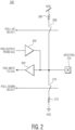
- FIG. 2 illustrates, in partial block diagram and partial schematic form, a GPIO pad circuit 200 coupled to a GPIO pad 214.
- GPIO pad 214 and pad circuit 200 can correspond to any of pad circuits and pads referred to in FIG. 1 and can be collectively referred to as an external terminal circuit.
- Pad circuit 200 includes resistors 206 and 212, switches 208 and 210, and buffers 202 and 204. A first terminal of resistor 206 is coupled to VDD, and a second terminal of resistor 206 is coupled to a first terminal of switch 208.
- a second terminal of switch 208 is coupled to GPIO pad 214, and a control input of switch 208 is coupled to receive a pull-up select signal which, when asserted, closes switch 208 such that switch 208 is in a conductive state, connecting its first and second terminals, and when negated, opens switch 208 such that switch 208 is in a non-conductive state, disconnecting its first and second terminals.
- a first terminal of switch 210 is coupled to GPIO pad 214, and a second terminal of switch 210 is coupled to a first terminal of resistor 212.
- a second terminal of resistor 212 is coupled to VSS.
- a control input of switch 210 is coupled to receive a pull-down select signal which, when asserted, closes switch 210 such that switch 210 is in a conductive state, connecting its first and second terminals, and when negated, opens switch 210 such that switch 210 is in a non-conductive state, disconnecting its first and second terminals.
- An input of buffer 202 is coupled to receive a pad output from IC 10, and an output of buffer 202 is coupled to GPIO pad 214.
- An input of buffer 204 is coupled to GPIO pad 214, and an output of buffer 204 is coupled to provide a pad input to IC 10. In the case that GPIO 214 is only an input pad, buffer 202 may not be present.
- GPIO pad 214 can receive inputs from pad 214 and provide outputs to pad 214, via buffers 204 and 202, respectively.
- the pull-up select and pull-down select signals are negated such that both switches 208 and 210 are open, or non-conductive.
- the pull-up select or pull-down select signal can be asserted such that pad 214 is not left floating.
- the input received by input buffer 204 and provided as inputs to IC 10 can be generated by asserting one of the pull-up select signal or the pull-down select signal to bias pad 214 appropriately, rather than receiving an external signal on pad 214 from a tester probe.
- the voltage on pad 214 obtained by asserting one of the pull-up or pull-down select signals may be referred to as the wakeup voltage which is translated to a digital high or low wakeup signal, respectively, at the output of buffer 204.
- pad circuit 200 operates at a first drive strength and a first current bias condition, but when IC 10 operates in low power mode, pad circuit 200 may operate at a second drive strength, lower than the first drive strength, and at a second current bias condition, lower than the first current bias condition.
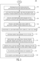
- IC 10 Operation of IC 10 will be described in reference to method 300 of FIG. 3 and the timing diagram of FIG. 4 .
- IC 10 For a low power mode test, IC 10, or portions thereof, are placed in a low power mode in which tests, such as current consumption tests, can be performed to ensure that IC 10 is correctly operating in low power mode (e.g. not surpassing current consumption limitations). It is also necessary to test that IC 10 properly exits low power mode when wakeup signals are received via those GPIO pads configured to receive wakeup signals, whether they are active-high or active-low wakeup signals. Therefore, prior to entering low power mode, appropriate control values are set up within IC 10, while IC 10 is still operating in normal mode and the resources are available. For example, this may include loading registers within IC 10 and latching values from those registers into storage circuits retain their contents during low power mode.
- pad expose register 14 is loaded with an appropriate pad select indicator and a corresponding high/low indicator.
- pad expose register 14 includes a pad select field which includes a pad select indicator for each of the N pads of IC 10 and a high/low indicator field.
- Each pad of IC 10 which is capable of receiving a wakeup signal, can be selected, in turn, for low power mode testing. Therefore, one of the N pads of IC 10 can be selected by storing a logic level one to the corresponding pad select indicator in register 14.
- a corresponding high/low indicator can be stored in the high/low indicator field of register 14, in which, in one embodiment, a logic level one indicates that the wakeup signal received on the selected pad is an active-high signal (indicating that a logic level high wakeup signal should trigger a wakeup of IC 10) and a logic level zero indicates that the wakeup signal received on the selected pad is an active-low signal (indicating that a logic level low wakeup signal should trigger a wakeup of IC 10).
- expose register 14 is part of debug circuitry of IC 10.
- the debug circuitry, including expose register 14, is not operational or accessible during low power mode. Therefore, as indicated in block 304 of method 300, prior to entering low power mode, the selected pad indicated by pad exposure register 14 along the high/low indicator of pad exposure register 14 are latched into pad select 26 and high/low indicator 28, respectively, of wakeup trigger generation circuit 16, and into channel select 36 and high/low indicator 34, respectively, of wakeup detector circuit 20. Note that, at this time, a timer value can also be stored in timer 30 in preparation for low power mode testing. During low power, both wakeup trigger generation circuit 16 and wakeup detector circuit 20 are operational, and therefore, the selected pad and corresponding high/low indicator are kept functional in these respective circuits even when in low power mode.
- a low power entry request is received by PCU 18 from CPU 12, requesting that IC 10 or portions of IC 10 enter the low power mode.
- PCU 18 initiates the low power entry sequence. That is, PCU 18 initiates the sequence required within IC 10 to enter the low power mode.
- PCU 18 Upon completing the sequence and entering the low power mode, PCU 18 asserts the low power mode entry complete signal which is received by wakeup trigger generation circuit 16 (as indicated in block 308).
- wakeup trigger generation circuit 16 starts test timer 30 (as indicated in block 310). While timer 30 is counting, prior to expiration, current measurement tests can be performed by an external tester in order to, for example, determine current consumption while IC 10 is operating in low power mode. Alternatively, other or additional tests may be performed.
- the appropriate trigger high and trigger low signals are provided to the selected pad, indicated by pad select 26, in order to generate the desired wakeup voltage on the selected pad.
- the selected pad indicated by pad select 26
- trigger high 1 and trigger low 1 are provided to MUXes 36 and 38, respectively.
- MUXes 36 and 38 may receive a control signal from PCU 18 (such as the low power mode entry complete signal itself) to select the trigger high 1 and trigger low 1 inputs, respectively, to be provided to the pull-up select input and pull-down select input, respectively, of pad circuit 22.
- trigger high/low indicator 28 indicates a trigger high, then trigger high 1 is asserted and trigger low 1 is negated such that the pull-up switch (corresponding to switch 208 within pad circuit 22) is closed and the appropriate logic level high voltage is provided by VDD via resistor 206 to input buffer 204. If, on the other hand, trigger high/low indicator 28 indicates a trigger low, then trigger low 1 is asserted and trigger high 1 is negated such that the pull-down switch (corresponding to switch 212 of pad circuit 22) is closed such that the appropriate logic level low voltage is provided by VSS via resistor 212 to input buffer 204. The appropriate wakeup voltage is provided via buffer 204 as the wakeup 1 signal to wakeup detector circuit 20.
- pad select 26 indicates a different pad, such as pad 3
- the appropriate trigger high 3 and trigger low 3 signals would be provided to the corresponding pad circuit for pad 3.
- the appropriate wakeup voltage is provided via the input buffer of the pad circuit for pad 3 as the wakeup 3 signal to wakeup detector circuit 20.
- Wakeup detector circuit 20 using channel select 36, monitors the appropriate channel to determine if the appropriate wakeup signal is received. For example, in the case of pad select 26 and channel select 36 indicating pad 1, wakeup detector circuit 20 monitors its ch1 input at which it expects to receive the wakeup 1 signal. Also, high/low indicator 34 indicates whether the wakeup 1 signal is expected to be a logic level high or logic level low. Assuming wakeup detector circuit 20 receives the expected wakeup signal on ch1, wakeup circuit 20, in block 316, asserts the async wakeup signal which is provided to PCU 18. In block 318, in response to the asserted async wakeup signal, PCU 18 initiates a low power exit sequence.
- PCU 18 asserts the low power mode exit complete signal which is provided to CPU 12. If CPU 12 properly exits the low power mode, then the wakeup signal was properly received from the pad circuit selected by pad expose register 14. If CPU 12 does not properly exit the low power mode, then an error occurred in the communication of a wakeup signal from the selected pad back to PCU 18. In this manner, each pad can be tested, in turn, via pad expose register 14 by repeating method 300 with a different selected pad. Furthermore, each pad can be tested without needing a probe contacting the corresponding GPIO pad itself since the appropriate wakeup signal is generated via the pull-up and pull-sown select switches rather than an input probe on the pad. This reduces the number of probes needed and thus enabled increased testing parallelism and improved testing efficiency.
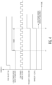
- FIG. 4 illustrates, in timing diagram form, various signals of IC 10, including pad select 26, the low power mode entry complete signal, the low power mode clock, trigger 1 high/low signal, and a wakeup signal (corresponding to wakeup 1 on channel 1, ch1, of wakeup detector circuit 20.
- the first signal from the top refers to pad select 26, whose assertion to a logic level one indicates when pad select 26 (and high/low indicator 28) are latched from debug pad expose register 14.
- the low power entry signal is asserted by PCU 18.
- timer 30 in wakeup trigger generation circuit 16 starts counting a predetermined window of time, which ends at time t2.
- low power mode testing can be performed by an external tester, such as current consumption tests.
- timer value of timer 30 can be set or adjusted as needed based on the low power mode testing needed during that time, but should end prior to entering the low power mode. This can be done, for example, by CPU 12.
- timer 30 counts down its timer value using the low power mode clock.
- the appropriate trigger high/low signals are provided to the appropriate pad circuit. For example, the assertion of the trigger 1 high/low signals in FIG. 4 indicates that the appropriate values of trigger 1 high and trigger 1 low are provided to pad circuit 22 based on high/low indicator 28.
- trigger 1 high is asserted and trigger 1 low is negated such that an active high wakeup signal is provided as wakeup 1 on channel 1 of wakeup detector circuit 20. Therefore, in FIG. 4 , at time t2, the appropriate wakeup voltage is provided at pad 214 based on trigger 1 high and trigger 1 low, and in response thereto, the wakeup 1 signal on channel 1 is asserted. This initiates the low power mode wakeup sequence (and results in assertion of the async wakeup signal).
- FIG. 5 illustrates, in block diagram form, an SoC 500, in accordance with one embodiment of the present invention.
- SoC 500 includes a plurality of GPIO pads 512, 514, 516, 518, 520, 522, 524, and 526, a logic/memory BIST circuit 504, an AC testing circuit 506, an analog test circuit 508, and a low power mode test circuit 510.
- SoC 500 is coupled to an external tester 502 via input and output probes which can each contact GPIO pads of SoC 500 as needed.
- BIST circuit 504 is coupled to GPIO pads 512 which are configured to receive test inputs via input probes of tester 502 and coupled to GPIO pads 520 which are configured to provide test outputs via output probes to tester 502.
- AC testing circuit 506 is coupled to GPIO pads 514 which are configured to receive test inputs via input probes of tester 502 and coupled to GPIO pads 522 which are configured to provide test outputs via output probes to tester 502.
- Analog test circuit 508 is coupled to GPIO pads 516 which are configured to receive test inputs via input probes of tester 502 and coupled to GPIO pads 524 which are configured to provide test outputs via output probes to tester 502. Any known circuitry can be used within test circuits 504, 506, and 508.
- Low power mode test circuit 510 is coupled to GPIO pads 518 which are configured to receive test inputs via input probes of tester 502 and coupled to GPIO pads 526 which are configured to provide test outputs via output probes to tester 502. Each of GPIO pads 518 and GPIO pads 526 can be implemented with the pad circuits as illustrated in FIGs. 1 and 2 .
- Low power mode test circuit 510 may include any low power mode test circuitry in which tester 502 can use input and output probes as needed to contact any of GPIO pads 518 and 526.
- Low power mode test circuit 510 may include a wakeup trigger generation circuit such as wakeup trigger generation circuit 16 and a wakeup detector circuit such as wakeup detector circuit 20 and may also include the test circuitry required to take current measurements during low power mode.
- SoC 500 like IC 10, may include any other circuitry, including a PCU, CPU, debug circuitry which may include the debug pad expose register, etc., or any other circuitry as needed.
- a wakeup trigger generation circuit to generate appropriate wakeup signals at selected GPIO pads during a low power test mode allows for the entry into and exit from low power mode to be tested without the need to contact probes themselves to those GPIO pads. This increases testing efficiency and allows for increased testing parallelism. Also, a timer mechanism in the wakeup trigger generation circuit allows for a window of time when other low power mode tests can be performed, in which current consumption measurements can be made.
- assert or “set” and “negate” (or “deassert” or “clear”) are used herein when referring to the rendering of a signal, status bit, or similar apparatus into its logically true or logically false state, respectively. If the logically true state is a logic level one, the logically false state is a logic level zero. And if the logically true state is a logic level zero, the logically false state is a logic level one.
- Each signal described herein may be designed as positive or negative logic, where negative logic can be indicated by a bar over the signal name or an asterix (*) following the name.
- negative logic the signal is active low where the logically true state corresponds to a logic level zero.
- positive logic the signal is active high where the logically true state corresponds to a logic level one.
- any of the signals described herein can be designed as either negative or positive logic signals. Therefore, in alternate embodiments, those signals described as positive logic signals may be implemented as negative logic signals, and those signals described as negative logic signals may be implemented as positive logic signals.
- the illustrated elements of IC 10 are circuitry located on a single integrated circuit or within a same device.
- system 10 may include any number of separate integrated circuits or separate devices interconnected with each other.
- Coupled is not intended to be limited to a direct coupling or a mechanical coupling.
- an integrated circuit includes a plurality of external terminal circuits, each external terminal circuit of the plurality including an external terminal; a wakeup detector including a plurality of inputs, each input of the plurality of inputs is coupled to an external terminal circuit of the plurality of external terminal circuits, wherein the wakeup detector generates an output signal indicative of an external terminal of the plurality of external terminal circuits being placed at a wakeup voltage; a trigger generation circuit, the trigger generation circuit including a plurality of outputs, each output of the plurality of outputs coupled to an external terminal circuit of the plurality to generate a wake up voltage at an external terminal of the external terminal circuit by coupling the external terminal to a power supply terminal of the integrated circuit to generate an indication of the external terminal being at the wakeup voltage at the wakeup detector when at least a portion of the integrated circuit is in a low power mode.
- the generation of the output signal indicative of an external terminal of the plurality of external terminal circuits being placed at a wakeup voltage causes the at least a portion of the integrated circuit to exit the low power mode.
- each external terminal circuit of the plurality when the at least a portion of the integrated circuit is in the low power, each external terminal circuit of the plurality operates at a first drive strength and at a first current bias condition, wherein when the at least a portion of the integrated circuit is in a normal operating mode, the each external terminal circuit operates at a second drive strength and at a second current bias condition, wherein the second drive strength is higher than the first drive strength and the second current bias condition is higher than the first current bias condition.
- the trigger generation circuit selectively asserts a signal on an output of the plurality of outputs to generate a wake-up voltage at an external terminal of a selected external terminal circuit of the plurality of external terminal circuits.
- the plurality of outputs of the trigger generation circuit includes a plurality of high voltage generation outputs and a plurality of low voltage generation outputs, wherein each high voltage generation output of the plurality of high voltage generation outputs is coupled to a corresponding external terminal circuit of the plurality of external terminal circuits to generate a high voltage wake up voltage at an external terminal of the corresponding external terminal circuit, wherein each low voltage generation output of the plurality of low voltage generation outputs is coupled to a corresponding external terminal circuit of the plurality of external terminal circuits to generate a low voltage wake up voltage at an external terminal of the corresponding external terminal circuit.
- the trigger generation circuit includes a timer, wherein the trigger generation circuit asserts a signal at an output of the plurality of outputs in response to a timed count of the timer to generate a wake-up voltage at an external terminal of an external terminal circuit of the plurality corresponding to the output.
- the timed count begins in response to an assertion of a low power indication received by the trigger generation circuit.
- the low power indication is provided by a power control circuit, wherein the output signal provided by the wake-up detector, indicative of an external terminal of the plurality of external terminal circuits being placed at a wakeup voltage is provided to the power control unit.
- the trigger generation circuit includes a register to receive an indication of a selected external terminal circuit of the plurality of external terminal circuits to generate a wake-up voltage at an external terminal of the selected external terminal circuit.
- each external terminal circuit of the plurality includes a switch for biasing an external terminal of the each external terminal circuit at a wake up voltage from the power supply terminal, wherein the each external terminal circuit includes a multiplexer including an output connected to a control terminal of the switch of the each external terminal circuit and including a plurality of inputs, wherein an output of the plurality of outputs of the trigger generation circuit is coupled to an input of the plurality of inputs of the multiplexer.
- each external terminal circuit of the plurality includes a switch for biasing an external terminal of each external terminal circuit at a wake-up voltage from the power supply terminal, wherein the assertion of a signal on an output of the plurality of outputs causes the switch to close to bias the external terminal at the wake-up voltage.
- the plurality of outputs of the trigger generation circuit includes a first plurality of outputs, each for generating a higher wakeup voltage at an external terminal of the plurality of external terminal circuits by coupling the external terminal to a first power supply voltage terminal, wherein the plurality of outputs of the trigger generation circuit includes a second plurality of outputs, each for generating a lower wakeup voltage at an external terminal of the plurality of external terminal circuits by coupling the external terminal to a second power supply voltage terminal, the second power supply voltage terminal is configured to supply a lower voltage than the first power supply terminal.
- a method of operating an integrated circuit includes asserting a signal on a selected output of a plurality of outputs of a trigger circuit of an integrated circuit; in response to the assertion of the signal, generating a voltage at an external terminal of a selected external terminal circuit of the integrated circuit corresponding to the selected output; wherein the generating a voltage causes a wake-up circuit of the integrated circuit to generate an indication that an external terminal of the integrated circuit is at a wake-up voltage.
- the asserting occurs when at least a portion of the integrated circuit is in a low power mode, wherein the indication that an external terminal of the integrated circuit is at a wake-up voltage causes the at least a portion of the integrated circuit to exit the low power mode.
- the selected external terminal circuit when the at least a portion of the integrated circuit is in the low power, operates at a first drive strength and at a first current bias condition, wherein when the at least a portion of the integrated circuit is in a normal operating mode, the selected external terminal circuit operates at a second drive strength and at a second current bias condition, wherein the second drive strength is higher than the first drive strength and the second current bias condition is higher than the first current bias condition.
- the method further includes receiving a signal by the trigger circuit indicative that at least a portion of the integrated circuit is in a low power mode, wherein the asserting is performed at a predetermined time after the receiving.
- the method further includes after receiving the signal and prior to the asserting, performing current measurement tests on the integrated circuit.
- the method further includes providing to the trigger circuit an indication of the selected external terminal circuit from the plurality of external terminal circuits for the asserting the signal on the selected output corresponding to the selected external terminal circuit.
- the trigger circuit includes two outputs of the plurality of outputs corresponding to the selected external terminal circuit, where a signal is asserted on a first output of the two outputs to provide a high wake up voltage at the external terminal and wherein a signal is asserted on the second output of the two outputs to provide a low wake up voltage at the external terminal, wherein prior to the asserting the signal on the selected output, the trigger circuit receives an indication of which of the two outputs is the selected output.
- an integrated circuit includes a plurality of external terminal circuits, each external terminal circuit of the plurality including an external terminal, each external terminal circuit of the plurality is coupled to two corresponding outputs of a plurality of outputs, wherein a first output of the two corresponding outputs is for generating a higher voltage at the external terminal of an external terminal circuit by coupling the external terminal to a first power supply voltage terminal of the integrated circuit and the second output of the two corresponding outputs is for generating a lower voltage at the external terminal of the external terminal circuit by coupling the external terminal to a second power supply voltage terminal that is configured to supply a lower voltage than the first power supply terminal; a wakeup detector, including a plurality of inputs, with each input of the plurality of inputs is coupled to an external terminal circuit of the plurality of external terminal circuits, wherein the wakeup detector provides an output signal indicative of an external terminal of the plurality of external terminal circuits being placed at a wakeup voltage; and a trigger generation circuit, the trigger generation circuit including the plurality of output
- An integrated circuit includes a plurality of external terminal circuits, each having an external terminal.
- the integrated circuit includes a wakeup detector including a plurality of inputs. Each input of the plurality of inputs is coupled to an external terminal circuit.
- the wakeup detector generates an output signal indicative of an external terminal of the plurality of external terminal circuits being placed at a wakeup voltage.
- the integrated circuit includes a trigger generation circuit having a plurality of outputs in which each output is coupled to an external terminal circuit to generate a wake-up voltage at an external terminal of the external terminal circuit by coupling the external terminal to a power supply terminal of the integrated circuit to generate an indication of the external terminal being at the wakeup voltage at the wakeup detector when at least a portion of the integrated circuit is in a low power mode.
Landscapes
- Engineering & Computer Science (AREA)
- Physics & Mathematics (AREA)
- General Engineering & Computer Science (AREA)
- General Physics & Mathematics (AREA)
- Computer Hardware Design (AREA)
- Microelectronics & Electronic Packaging (AREA)
- Environmental & Geological Engineering (AREA)
- Theoretical Computer Science (AREA)
- Health & Medical Sciences (AREA)
- Toxicology (AREA)
- Semiconductor Integrated Circuits (AREA)
Claims (15)
- Integrierte Schaltung (10), Folgendes umfassend:mehrere externe Anschlussschaltungen (22), wobei jede externe Anschlussschaltung der mehreren externen Anschlussschaltungen einen externen Anschluss (214) umfasst; undeinen Puffer (204), Folgendes umfassend:einen Eingangsanschluss des Puffers, der an den externen Anschluss angeschlossen ist, undeinen Ausgangsanschluss des Puffers, der angeschlossen ist, um einen Eingang in die integrierte Schaltung bereitzustellen, einen Reaktivierungsdetektor (20), der mehrere Eingänge umfasst, wobei jeder Eingang von den mehreren Eingängen an eine externe Anschlussschaltung der mehreren externen Anschlussschaltungen angeschlossen ist, wobei der Reaktivierungsdetektor ein Ausgangssignal erzeugt, das für einen externen Anschluss der mehreren externen Anschlussschaltungen bezeichnend ist, die unter eine Reaktivierungsspannung gesetzt werden;eine Trigger-Erzeugungsschaltung (16), wobei die Trigger-Erzeugungsschaltung mehrere Ausgänge umfasst, jeder Ausgang der mehreren Ausgänge an eine externe Anschlussschaltung der mehreren externen Anschlussschaltungen angeschlossen ist, um eine Reaktivierungsspannung an einem externen Anschluss der externen Anschlussschaltung durch Anschließen des externen Anschlusses an einen Stromversorgungsanschluss der integrierten Schaltung zu erzeugen, um eine Angabe, dass der externe Anschluss unter die Reaktivierungsspannung gesetzt wurde, über den Puffer (204) an dem Reaktivierungsdetektor zu erzeugen, wenn mindestens ein Abschnitt der integrierten Schaltung in einer Kleinleistungsbetriebsart ist.
- Integrierte Schaltung (10) nach Anspruch 1, wobei die Erzeugung des Ausgangssignals, das bezeichnend ist, dass ein externer Anschluss (214) der mehreren externen Anschlussschaltungen (22) unter eine Reaktivierungsspannung gesetzt wurde, bewirkt, dass der mindestens eine Abschnitt der integrierten Schaltung die Kleinleistungsbetriebsart verlässt.
- Integrierte Schaltung (10) nach Anspruch 1 oder 2, wobei, wenn der mindestens eine Abschnitt der integrierten Schaltung in der Kleinleistungsbetriebsart ist, jede externe Anschlussschaltung (22) der mehreren externen Anschlussschaltungen bei einer ersten Treiberstärke und bei einem ersten Vorspannungsstromzustand arbeitet, wobei, wenn der mindestens eine Abschnitt der integrierten Schaltung in einer normalen Betriebsart ist, jede externe Anschlussschaltung bei einer zweiten Treiberstärke und in einem zweiten Vorspannungsstromzustand arbeitet, wobei die zweite Treiberstärke größer ist als die erste Treiberstärke und der zweite Vorspannungsstromzustand größer ist als der erste Vorspannungsstromzustand.
- Integrierte Schaltung (10) nach einem vorhergehenden Anspruch, wobei die Trigger-Erzeugungsschaltung (16) ein Signal auf einem Ausgang der mehreren Ausgänge selektiv aktiviert, um eine Reaktivierungsspannung an einem externen Anschluss (214) einer ausgewählten externen Anschlussschaltung (22) der mehreren externen Anschlussschaltungen zu erzeugen.
- Integrierte Schaltung (10) nach einem vorhergehenden Anspruch, wobei die mehreren Ausgänge der Trigger-Erzeugungsschaltung (16) mehrere Hochspannungserzeugungausgänge und mehrere Niederspannungserzeugungsausgänge umfassen, wobei jeder Hochspannungserzeugungausgang der mehreren Hochspannungserzeugungausgänge an eine entsprechende externe Anschlussschaltung (22) der mehreren externen Anschlussschaltungen angeschlossen ist, um eine Reaktivierungshochspannung an einem externen Anschluss (214) der entsprechenden externen Anschlussschaltung zu erzeugen, wobei jeder Niederspannungserzeugungsausgang der mehreren Niederspannungserzeugungsausgänge an eine entsprechende externe Anschlussschaltung der mehreren externen Anschlussschaltungen angeschlossen ist, um eine Reaktivierungsniederspannung an einem externen Anschluss der entsprechenden externen Anschlussschaltung zu erzeugen.
- Integrierte Schaltung (10) nach einem vorhergehenden Anspruch, wobei die Trigger-Erzeugungsschaltung (16) einen Zeitgeber (30) umfasst, wobei die Trigger-Erzeugungsschaltung ein Signal an einem Ausgang der mehreren Ausgänge als Reaktion auf einen Zeitzähler des Zeitgebers aktiviert, um eine Reaktivierungsspannung an einem externen Anschluss (214) einer externen Anschlussschaltung (22) der mehreren externen Anschlussschaltungen entsprechend dem Ausgang zu erzeugen.
- Integrierte Schaltung (10) nach Anspruch 6, wobei der Zeitzähler als Reaktion auf ein Aktivieren einer Kleinleistungsangabe beginnt, die von der Trigger-Erzeugungsschaltung (16) empfangen wird.
- Integrierte Schaltung (10) nach Anspruch 7, wobei die Kleinleistungsangabe von einer Leistungssteuerungseinheit (18) bereitgestellt wird, wobei das Ausgangssignal, das von dem Reaktivierungsdetektor (20) bereitgestellt wird und bezeichnend ist, dass ein externer Anschluss (214) der mehreren externen Anschlussschaltungen (22) unter eine Reaktivierungsspannung gesetzt wird, der Leistungssteuerungseinheit bereitgestellt wird.
- Integrierte Schaltung (10) nach einem vorhergehenden Anspruch, wobei die Trigger-Erzeugungsschaltung (16) ein Register (14) umfasst, um eine Angabe einer ausgewählten externen Anschlussschaltung (214) der mehreren externen Anschlussschaltungen (22) zu empfangen, um eine Reaktivierungsspannung an einem externen Anschluss der ausgewählten externen Anschlussschaltung zu erzeugen.
- Integrierte Schaltung (10) nach einem vorhergehenden Anspruch, wobei jede externe Anschlussschaltung (22) der mehreren externen Anschlussschaltungen einen Schalter (208, 210) zum Vorspannen eines externen Anschlusses (214) jeder externen Anschlussschaltung mit einer Reaktivierungsspannung von dem Stromversorgungsanschluss umfasst, wobei jede externe Anschlussschaltung einen Multiplexer (36, 38, 40, 42) umfasst, der einen Ausgang umfasst, der mit einem Steuerungsanschluss des Schalters jeder externen Anschlussschaltung verbunden ist, und mehrere Eingänge umfasst, wobei ein Ausgang der mehreren Ausgänge der Trigger-Erzeugungsschaltung (16) an einen Eingang der mehreren Eingängen des Multiplexers angeschlossen ist.
- Integrierte Schaltung (10) nach einem vorhergehenden Anspruch, wobei jede externe Anschlussschaltung (22) der mehreren externen Anschlussschaltungen einen Schalter (208, 210) zum Vorspannen eines externen Anschlusses (214) jeder externen Anschlussschaltung mit einer Reaktivierungsspannung von dem Stromversorgungsanschluss umfasst, wobei das Aktivieren eines Signals auf einem Ausgang der mehreren Ausgänge bewirkt, dass der Schalter schließt, um den externen Anschluss mit der Reaktivierungsspannung vorzuspannen.
- Integrierte Schaltung (10) nach einem vorhergehenden Anspruch, wobei die mehreren Ausgänge der Trigger-Erzeugungsschaltung (16) eine erste Mehrzahl von Ausgängen umfassen, jeder zum Erzeugen einer höheren Reaktivierungsspannung an einem externen Anschluss der mehreren externen Anschlussschaltungen (22) durch Anschließen des externen Anschlusses (214) an einen ersten Stromversorgungsspannungsanschluss, wobei die mehreren Ausgänge der Trigger-Erzeugungsschaltung eine zweite Mehrzahl von Ausgängen umfassen, jeder zum Erzeugen einer niedrigeren Reaktivierungsspannung an einem externen Anschluss der mehreren externen Anschlussschaltungen durch Anschließen des externen Anschlusses an einen zweiten Stromversorgungsspannungsanschluss, wobei der zweite Stromversorgungsspannungsanschluss eingerichtet ist, um eine niedrigere Spannung als der erste Stromversorgungsanschluss zu liefern.
- Verfahren (300) zum Betreiben einer integrierten Schaltung nach einem der Ansprüche 1 bis 12, das Verfahren Folgendes umfassend:Aktivieren eines Signals auf einem ausgewählten Ausgang von mehreren Ausgängen einer Trigger-Erzeugungsschaltung einer integrierten Schaltung;als Reaktion auf das Aktivieren des Signals, Erzeugen (314) einer Spannung an einem externen Anschluss einer ausgewählten externen Anschlussschaltung der integrierten Schaltung entsprechend dem ausgewählten Ausgang;wobei das Erzeugen einer Spannung bewirkt, dass eine Reaktivierungsschaltung der integrierten Schaltung eine Angabe (316) erzeugt, dass ein externer Anschluss der integrierten Schaltung auf einer Reaktivierungsspannung ist.
- Verfahren nach Anspruch 13, wobei das Aktivieren auftritt, wenn mindestens ein Abschnitt der integrierten Schaltung in einer Kleinleistungsbetriebsart ist, wobei die Angabe, dass ein externer Anschluss der integrierten Schaltung auf einer Reaktivierungsspannung ist, bewirkt, dass der mindestens eine Abschnitt der integrierten Schaltung die Kleinleistungsbetriebsart (318) verlässt.
- Verfahren nach Anspruch 13 oder 14, wobei, wenn der mindestens eine Abschnitt der integrierten Schaltung in der Kleinleistungsbetriebsart ist, die ausgewählte externe Anschlussschaltung bei einer ersten Treiberstärke und bei einem ersten Vorspannungsstromzustand arbeitet, wobei, wenn der mindestens eine Abschnitt der integrierten Schaltung in einer normalen Betriebsart ist, die ausgewählte externe Anschlussschaltung bei einer zweiten Treiberstärke und in einem zweiten Vorspannungsstromzustand arbeitet, wobei die zweite Treiberstärke größer ist als die erste Treiberstärke und der zweite Vorspannungsstromzustand größer ist als der erste Vorspannungsstromzustand.
Applications Claiming Priority (1)
| Application Number | Priority Date | Filing Date | Title |
|---|---|---|---|
| US16/292,654 US11047904B2 (en) | 2019-03-05 | 2019-03-05 | Low power mode testing in an integrated circuit |
Publications (2)
| Publication Number | Publication Date |
|---|---|
| EP3705980A1 EP3705980A1 (de) | 2020-09-09 |
| EP3705980B1 true EP3705980B1 (de) | 2023-07-19 |
Family
ID=69743186
Family Applications (1)
| Application Number | Title | Priority Date | Filing Date |
|---|---|---|---|
| EP20160492.3A Active EP3705980B1 (de) | 2019-03-05 | 2020-03-02 | Niederstrommodusprüfung in einer integrierten schaltung |
Country Status (2)
| Country | Link |
|---|---|
| US (1) | US11047904B2 (de) |
| EP (1) | EP3705980B1 (de) |
Families Citing this family (2)
| Publication number | Priority date | Publication date | Assignee | Title |
|---|---|---|---|---|
| US11385982B2 (en) * | 2019-05-02 | 2022-07-12 | Apple Inc. | General purpose input/output with hysteresis |
| US12609695B2 (en) * | 2023-12-20 | 2026-04-21 | Nxp B.V. | Feedback based scalable method and system for avoiding failures during power mode transitions and subsequent wakeup |
Family Cites Families (13)
| Publication number | Priority date | Publication date | Assignee | Title |
|---|---|---|---|---|
| US6052746A (en) | 1998-04-14 | 2000-04-18 | Motorola, Inc. | Integrated circuit having programmable pull device configured to enable/disable first function in favor of second function according to predetermined scheme before/after reset |
| US6590225B2 (en) | 2001-01-19 | 2003-07-08 | Texas Instruments Incorporated | Die testing using top surface test pads |
| US7756197B1 (en) | 2003-11-26 | 2010-07-13 | Pmc-Sierra, Inc. | Built in self test (BIST) for high-speed serial transceivers |
| WO2007014053A2 (en) * | 2005-07-22 | 2007-02-01 | Nanopower Technologies, Inc. | High sensitivity rfid tag integrated circuits |
| US7274203B2 (en) * | 2005-10-25 | 2007-09-25 | Freescale Semiconductor, Inc. | Design-for-test circuit for low pin count devices |
| US8041973B2 (en) | 2007-05-03 | 2011-10-18 | Microchip Technology Incorporated | Interrupt/wake-up of an electronic device in a low power sleep mode when detecting a sensor or frequency source activated frequency change |
| US8040151B2 (en) * | 2008-12-19 | 2011-10-18 | Actel Corporation | Programmable logic device with programmable wakeup pins |
| JP2011007591A (ja) | 2009-06-25 | 2011-01-13 | Canon Inc | Asic及び基板の接続検査方法 |
| JP2011135150A (ja) * | 2009-12-22 | 2011-07-07 | Renesas Electronics Corp | D/aコンバータ回路及びその電圧供給制御方法 |
| US8543856B2 (en) * | 2011-08-20 | 2013-09-24 | Freescale Semiconductor Inc | Semiconductor device with wake-up unit |
| JP5902998B2 (ja) * | 2012-05-28 | 2016-04-13 | ルネサスエレクトロニクス株式会社 | 半導体集積回路およびその動作方法 |
| CN104751896B (zh) | 2015-04-17 | 2017-10-27 | 上海华虹宏力半导体制造有限公司 | 内建自测试电路 |
| CN118069218A (zh) * | 2017-09-12 | 2024-05-24 | 恩倍科微公司 | 极低功率微控制器系统 |
-
2019
- 2019-03-05 US US16/292,654 patent/US11047904B2/en active Active
-
2020
- 2020-03-02 EP EP20160492.3A patent/EP3705980B1/de active Active
Also Published As
| Publication number | Publication date |
|---|---|
| EP3705980A1 (de) | 2020-09-09 |
| US11047904B2 (en) | 2021-06-29 |
| US20200284830A1 (en) | 2020-09-10 |
Similar Documents
| Publication | Publication Date | Title |
|---|---|---|
| KR960005606B1 (ko) | 저 대역폭 검사 장비 및 프로브 스테이션을 사용하여 디지탈 마이크로회로의 단순 및 정확한 에이씨(ac) 검사를 제공하는 내장 검사 회로 및 속도 검사 방법 | |
| CN209231464U (zh) | 集成电路 | |
| US9459319B2 (en) | Device and method for generating input control signals of a serialized compressed scan circuit | |
| US9267989B2 (en) | Integrated circuit testing with power collapsed | |
| US20160091566A1 (en) | Integrated circuit wth low power scan flip-flop | |
| US9213063B2 (en) | Reset generation circuit for scan mode exit | |
| US8841952B1 (en) | Data retention flip-flop | |
| US5561614A (en) | Method and apparatus for testing pin isolation for an integrated circuit in a low power mode of operation | |
| EP3705980A1 (de) | Niederstrommodusprüfung in einer integrierten schaltung | |
| CN106680688B (zh) | 利用并行扫描测试数据输入和输出测试多核集成电路 | |
| US9599673B2 (en) | Structural testing of integrated circuits | |
| US7417450B2 (en) | Testing combinational logic die with bidirectional TDI-TMS/TDO chanel circuit | |
| CN211698063U (zh) | 电子设备 | |
| CN108872828B (zh) | 复位管理电路和用于复位管理电路的方法 | |
| US20240418776A1 (en) | Integrated-circuit chip for retention cell testing | |
| US7389452B2 (en) | Methods and apparatus for monitoring internal signals in an integrated circuit | |
| US8278960B2 (en) | Method and circuit for measuring quiescent current | |
| US11519960B2 (en) | Circuit configured to determine a test voltage suitable for very low voltage (VLV) testing in an integrated circuit | |
| US7228479B2 (en) | IEEE Std. 1149.4 compatible analog BIST methodology | |
| US9646717B2 (en) | Memory device with internal measurement of functional parameters | |
| US5548285A (en) | Circuit and method of indicating data hold-time | |
| US7281182B2 (en) | Method and circuit using boundary scan cells for design library analysis | |
| JP2008209201A (ja) | 電流測定方法及び半導体集積回路 | |
| TWI418821B (zh) | 測試系統 | |
| US11777483B1 (en) | On-die techniques for asynchnorously comparing voltages |
Legal Events
| Date | Code | Title | Description |
|---|---|---|---|
| PUAI | Public reference made under article 153(3) epc to a published international application that has entered the european phase |
Free format text: ORIGINAL CODE: 0009012 |
|
| STAA | Information on the status of an ep patent application or granted ep patent |
Free format text: STATUS: THE APPLICATION HAS BEEN PUBLISHED |
|
| AK | Designated contracting states |
Kind code of ref document: A1 Designated state(s): AL AT BE BG CH CY CZ DE DK EE ES FI FR GB GR HR HU IE IS IT LI LT LU LV MC MK MT NL NO PL PT RO RS SE SI SK SM TR |
|
| AX | Request for extension of the european patent |
Extension state: BA ME |
|
| STAA | Information on the status of an ep patent application or granted ep patent |
Free format text: STATUS: REQUEST FOR EXAMINATION WAS MADE |
|
| 17P | Request for examination filed |
Effective date: 20210309 |
|
| RBV | Designated contracting states (corrected) |
Designated state(s): AL AT BE BG CH CY CZ DE DK EE ES FI FR GB GR HR HU IE IS IT LI LT LU LV MC MK MT NL NO PL PT RO RS SE SI SK SM TR |
|
| GRAP | Despatch of communication of intention to grant a patent |
Free format text: ORIGINAL CODE: EPIDOSNIGR1 |
|
| STAA | Information on the status of an ep patent application or granted ep patent |
Free format text: STATUS: GRANT OF PATENT IS INTENDED |
|
| INTG | Intention to grant announced |
Effective date: 20230322 |
|
| GRAS | Grant fee paid |
Free format text: ORIGINAL CODE: EPIDOSNIGR3 |
|
| GRAA | (expected) grant |
Free format text: ORIGINAL CODE: 0009210 |
|
| STAA | Information on the status of an ep patent application or granted ep patent |
Free format text: STATUS: THE PATENT HAS BEEN GRANTED |
|
| AK | Designated contracting states |
Kind code of ref document: B1 Designated state(s): AL AT BE BG CH CY CZ DE DK EE ES FI FR GB GR HR HU IE IS IT LI LT LU LV MC MK MT NL NO PL PT RO RS SE SI SK SM TR |
|
| REG | Reference to a national code |
Ref country code: GB Ref legal event code: FG4D |
|
| REG | Reference to a national code |
Ref country code: CH Ref legal event code: EP |
|
| REG | Reference to a national code |
Ref country code: DE Ref legal event code: R096 Ref document number: 602020013913 Country of ref document: DE |
|
| REG | Reference to a national code |
Ref country code: IE Ref legal event code: FG4D |
|
| P01 | Opt-out of the competence of the unified patent court (upc) registered |
Effective date: 20230907 |
|
| REG | Reference to a national code |
Ref country code: LT Ref legal event code: MG9D |
|
| REG | Reference to a national code |
Ref country code: NL Ref legal event code: MP Effective date: 20230719 |
|
| REG | Reference to a national code |
Ref country code: AT Ref legal event code: MK05 Ref document number: 1590115 Country of ref document: AT Kind code of ref document: T Effective date: 20230719 |
|
| PG25 | Lapsed in a contracting state [announced via postgrant information from national office to epo] |
Ref country code: NL Free format text: LAPSE BECAUSE OF FAILURE TO SUBMIT A TRANSLATION OF THE DESCRIPTION OR TO PAY THE FEE WITHIN THE PRESCRIBED TIME-LIMIT Effective date: 20230719 |
|
| PG25 | Lapsed in a contracting state [announced via postgrant information from national office to epo] |
Ref country code: GR Free format text: LAPSE BECAUSE OF FAILURE TO SUBMIT A TRANSLATION OF THE DESCRIPTION OR TO PAY THE FEE WITHIN THE PRESCRIBED TIME-LIMIT Effective date: 20231020 |
|
| PG25 | Lapsed in a contracting state [announced via postgrant information from national office to epo] |
Ref country code: IS Free format text: LAPSE BECAUSE OF FAILURE TO SUBMIT A TRANSLATION OF THE DESCRIPTION OR TO PAY THE FEE WITHIN THE PRESCRIBED TIME-LIMIT Effective date: 20231119 |
|
| PG25 | Lapsed in a contracting state [announced via postgrant information from national office to epo] |
Ref country code: SE Free format text: LAPSE BECAUSE OF FAILURE TO SUBMIT A TRANSLATION OF THE DESCRIPTION OR TO PAY THE FEE WITHIN THE PRESCRIBED TIME-LIMIT Effective date: 20230719 Ref country code: RS Free format text: LAPSE BECAUSE OF FAILURE TO SUBMIT A TRANSLATION OF THE DESCRIPTION OR TO PAY THE FEE WITHIN THE PRESCRIBED TIME-LIMIT Effective date: 20230719 Ref country code: PT Free format text: LAPSE BECAUSE OF FAILURE TO SUBMIT A TRANSLATION OF THE DESCRIPTION OR TO PAY THE FEE WITHIN THE PRESCRIBED TIME-LIMIT Effective date: 20231120 Ref country code: NO Free format text: LAPSE BECAUSE OF FAILURE TO SUBMIT A TRANSLATION OF THE DESCRIPTION OR TO PAY THE FEE WITHIN THE PRESCRIBED TIME-LIMIT Effective date: 20231019 Ref country code: LV Free format text: LAPSE BECAUSE OF FAILURE TO SUBMIT A TRANSLATION OF THE DESCRIPTION OR TO PAY THE FEE WITHIN THE PRESCRIBED TIME-LIMIT Effective date: 20230719 Ref country code: LT Free format text: LAPSE BECAUSE OF FAILURE TO SUBMIT A TRANSLATION OF THE DESCRIPTION OR TO PAY THE FEE WITHIN THE PRESCRIBED TIME-LIMIT Effective date: 20230719 Ref country code: IS Free format text: LAPSE BECAUSE OF FAILURE TO SUBMIT A TRANSLATION OF THE DESCRIPTION OR TO PAY THE FEE WITHIN THE PRESCRIBED TIME-LIMIT Effective date: 20231119 Ref country code: HR Free format text: LAPSE BECAUSE OF FAILURE TO SUBMIT A TRANSLATION OF THE DESCRIPTION OR TO PAY THE FEE WITHIN THE PRESCRIBED TIME-LIMIT Effective date: 20230719 Ref country code: GR Free format text: LAPSE BECAUSE OF FAILURE TO SUBMIT A TRANSLATION OF THE DESCRIPTION OR TO PAY THE FEE WITHIN THE PRESCRIBED TIME-LIMIT Effective date: 20231020 Ref country code: FI Free format text: LAPSE BECAUSE OF FAILURE TO SUBMIT A TRANSLATION OF THE DESCRIPTION OR TO PAY THE FEE WITHIN THE PRESCRIBED TIME-LIMIT Effective date: 20230719 Ref country code: AT Free format text: LAPSE BECAUSE OF FAILURE TO SUBMIT A TRANSLATION OF THE DESCRIPTION OR TO PAY THE FEE WITHIN THE PRESCRIBED TIME-LIMIT Effective date: 20230719 |
|
| PG25 | Lapsed in a contracting state [announced via postgrant information from national office to epo] |
Ref country code: PL Free format text: LAPSE BECAUSE OF FAILURE TO SUBMIT A TRANSLATION OF THE DESCRIPTION OR TO PAY THE FEE WITHIN THE PRESCRIBED TIME-LIMIT Effective date: 20230719 |
|
| REG | Reference to a national code |
Ref country code: DE Ref legal event code: R097 Ref document number: 602020013913 Country of ref document: DE |
|
| PG25 | Lapsed in a contracting state [announced via postgrant information from national office to epo] |
Ref country code: ES Free format text: LAPSE BECAUSE OF FAILURE TO SUBMIT A TRANSLATION OF THE DESCRIPTION OR TO PAY THE FEE WITHIN THE PRESCRIBED TIME-LIMIT Effective date: 20230719 |
|
| PG25 | Lapsed in a contracting state [announced via postgrant information from national office to epo] |
Ref country code: SM Free format text: LAPSE BECAUSE OF FAILURE TO SUBMIT A TRANSLATION OF THE DESCRIPTION OR TO PAY THE FEE WITHIN THE PRESCRIBED TIME-LIMIT Effective date: 20230719 Ref country code: RO Free format text: LAPSE BECAUSE OF FAILURE TO SUBMIT A TRANSLATION OF THE DESCRIPTION OR TO PAY THE FEE WITHIN THE PRESCRIBED TIME-LIMIT Effective date: 20230719 Ref country code: ES Free format text: LAPSE BECAUSE OF FAILURE TO SUBMIT A TRANSLATION OF THE DESCRIPTION OR TO PAY THE FEE WITHIN THE PRESCRIBED TIME-LIMIT Effective date: 20230719 Ref country code: EE Free format text: LAPSE BECAUSE OF FAILURE TO SUBMIT A TRANSLATION OF THE DESCRIPTION OR TO PAY THE FEE WITHIN THE PRESCRIBED TIME-LIMIT Effective date: 20230719 Ref country code: DK Free format text: LAPSE BECAUSE OF FAILURE TO SUBMIT A TRANSLATION OF THE DESCRIPTION OR TO PAY THE FEE WITHIN THE PRESCRIBED TIME-LIMIT Effective date: 20230719 Ref country code: CZ Free format text: LAPSE BECAUSE OF FAILURE TO SUBMIT A TRANSLATION OF THE DESCRIPTION OR TO PAY THE FEE WITHIN THE PRESCRIBED TIME-LIMIT Effective date: 20230719 Ref country code: SK Free format text: LAPSE BECAUSE OF FAILURE TO SUBMIT A TRANSLATION OF THE DESCRIPTION OR TO PAY THE FEE WITHIN THE PRESCRIBED TIME-LIMIT Effective date: 20230719 |
|
| PLBE | No opposition filed within time limit |
Free format text: ORIGINAL CODE: 0009261 |
|
| STAA | Information on the status of an ep patent application or granted ep patent |
Free format text: STATUS: NO OPPOSITION FILED WITHIN TIME LIMIT |
|
| PG25 | Lapsed in a contracting state [announced via postgrant information from national office to epo] |
Ref country code: IT Free format text: LAPSE BECAUSE OF FAILURE TO SUBMIT A TRANSLATION OF THE DESCRIPTION OR TO PAY THE FEE WITHIN THE PRESCRIBED TIME-LIMIT Effective date: 20230719 |
|
| PGFP | Annual fee paid to national office [announced via postgrant information from national office to epo] |
Ref country code: FR Payment date: 20240220 Year of fee payment: 5 |
|
| 26N | No opposition filed |
Effective date: 20240422 |
|
| PG25 | Lapsed in a contracting state [announced via postgrant information from national office to epo] |
Ref country code: SI Free format text: LAPSE BECAUSE OF FAILURE TO SUBMIT A TRANSLATION OF THE DESCRIPTION OR TO PAY THE FEE WITHIN THE PRESCRIBED TIME-LIMIT Effective date: 20230719 |
|
| REG | Reference to a national code |
Ref country code: CH Ref legal event code: PL |
|
| PG25 | Lapsed in a contracting state [announced via postgrant information from national office to epo] |
Ref country code: BG Free format text: LAPSE BECAUSE OF FAILURE TO SUBMIT A TRANSLATION OF THE DESCRIPTION OR TO PAY THE FEE WITHIN THE PRESCRIBED TIME-LIMIT Effective date: 20230719 |
|
| PG25 | Lapsed in a contracting state [announced via postgrant information from national office to epo] |
Ref country code: LU Free format text: LAPSE BECAUSE OF NON-PAYMENT OF DUE FEES Effective date: 20240302 |
|
| PG25 | Lapsed in a contracting state [announced via postgrant information from national office to epo] |
Ref country code: MC Free format text: LAPSE BECAUSE OF FAILURE TO SUBMIT A TRANSLATION OF THE DESCRIPTION OR TO PAY THE FEE WITHIN THE PRESCRIBED TIME-LIMIT Effective date: 20230719 |
|
| GBPC | Gb: european patent ceased through non-payment of renewal fee |
Effective date: 20240302 |
|
| PG25 | Lapsed in a contracting state [announced via postgrant information from national office to epo] |
Ref country code: MC Free format text: LAPSE BECAUSE OF FAILURE TO SUBMIT A TRANSLATION OF THE DESCRIPTION OR TO PAY THE FEE WITHIN THE PRESCRIBED TIME-LIMIT Effective date: 20230719 Ref country code: LU Free format text: LAPSE BECAUSE OF NON-PAYMENT OF DUE FEES Effective date: 20240302 Ref country code: BG Free format text: LAPSE BECAUSE OF FAILURE TO SUBMIT A TRANSLATION OF THE DESCRIPTION OR TO PAY THE FEE WITHIN THE PRESCRIBED TIME-LIMIT Effective date: 20230719 |
|
| REG | Reference to a national code |
Ref country code: BE Ref legal event code: MM Effective date: 20240331 |
|
| PG25 | Lapsed in a contracting state [announced via postgrant information from national office to epo] |
Ref country code: BE Free format text: LAPSE BECAUSE OF NON-PAYMENT OF DUE FEES Effective date: 20240331 |
|
| PG25 | Lapsed in a contracting state [announced via postgrant information from national office to epo] |
Ref country code: GB Free format text: LAPSE BECAUSE OF NON-PAYMENT OF DUE FEES Effective date: 20240302 |
|
| PG25 | Lapsed in a contracting state [announced via postgrant information from national office to epo] |
Ref country code: IE Free format text: LAPSE BECAUSE OF NON-PAYMENT OF DUE FEES Effective date: 20240302 |
|
| PG25 | Lapsed in a contracting state [announced via postgrant information from national office to epo] |
Ref country code: IE Free format text: LAPSE BECAUSE OF NON-PAYMENT OF DUE FEES Effective date: 20240302 Ref country code: GB Free format text: LAPSE BECAUSE OF NON-PAYMENT OF DUE FEES Effective date: 20240302 Ref country code: BE Free format text: LAPSE BECAUSE OF NON-PAYMENT OF DUE FEES Effective date: 20240331 Ref country code: CH Free format text: LAPSE BECAUSE OF NON-PAYMENT OF DUE FEES Effective date: 20240331 |
|
| PG25 | Lapsed in a contracting state [announced via postgrant information from national office to epo] |
Ref country code: CY Free format text: LAPSE BECAUSE OF FAILURE TO SUBMIT A TRANSLATION OF THE DESCRIPTION OR TO PAY THE FEE WITHIN THE PRESCRIBED TIME-LIMIT; INVALID AB INITIO Effective date: 20200302 |
|
| PG25 | Lapsed in a contracting state [announced via postgrant information from national office to epo] |
Ref country code: HU Free format text: LAPSE BECAUSE OF FAILURE TO SUBMIT A TRANSLATION OF THE DESCRIPTION OR TO PAY THE FEE WITHIN THE PRESCRIBED TIME-LIMIT; INVALID AB INITIO Effective date: 20200302 |
|
| PG25 | Lapsed in a contracting state [announced via postgrant information from national office to epo] |
Ref country code: TR Free format text: LAPSE BECAUSE OF FAILURE TO SUBMIT A TRANSLATION OF THE DESCRIPTION OR TO PAY THE FEE WITHIN THE PRESCRIBED TIME-LIMIT Effective date: 20230719 |
|
| PG25 | Lapsed in a contracting state [announced via postgrant information from national office to epo] |
Ref country code: FR Free format text: LAPSE BECAUSE OF NON-PAYMENT OF DUE FEES Effective date: 20250331 |
|
| PGFP | Annual fee paid to national office [announced via postgrant information from national office to epo] |
Ref country code: DE Payment date: 20260219 Year of fee payment: 7 |