EP3703121A1 - Semiconductor device and method for manufacturing semiconductor device - Google Patents
Semiconductor device and method for manufacturing semiconductor device Download PDFInfo
- Publication number
- EP3703121A1 EP3703121A1 EP17930124.7A EP17930124A EP3703121A1 EP 3703121 A1 EP3703121 A1 EP 3703121A1 EP 17930124 A EP17930124 A EP 17930124A EP 3703121 A1 EP3703121 A1 EP 3703121A1
- Authority
- EP
- European Patent Office
- Prior art keywords
- terminal
- control
- connector
- substrate
- conductive layer
- Prior art date
- Legal status (The legal status is an assumption and is not a legal conclusion. Google has not performed a legal analysis and makes no representation as to the accuracy of the status listed.)
- Granted
Links
Images






Classifications
-
- H—ELECTRICITY
- H10—SEMICONDUCTOR DEVICES; ELECTRIC SOLID-STATE DEVICES NOT OTHERWISE PROVIDED FOR
- H10W—GENERIC PACKAGES, INTERCONNECTIONS, CONNECTORS OR OTHER CONSTRUCTIONAL DETAILS OF DEVICES COVERED BY CLASS H10
- H10W70/00—Package substrates; Interposers; Redistribution layers [RDL]
- H10W70/01—Manufacture or treatment
- H10W70/05—Manufacture or treatment of insulating or insulated package substrates, or of interposers, or of redistribution layers
- H10W70/093—Connecting or disconnecting other interconnections thereto or therefrom, e.g. connecting bond wires or bumps
-
- H—ELECTRICITY
- H10—SEMICONDUCTOR DEVICES; ELECTRIC SOLID-STATE DEVICES NOT OTHERWISE PROVIDED FOR
- H10W—GENERIC PACKAGES, INTERCONNECTIONS, CONNECTORS OR OTHER CONSTRUCTIONAL DETAILS OF DEVICES COVERED BY CLASS H10
- H10W90/00—Package configurations
- H10W90/701—Package configurations characterised by the relative positions of pads or connectors relative to package parts
-
- H—ELECTRICITY
- H10—SEMICONDUCTOR DEVICES; ELECTRIC SOLID-STATE DEVICES NOT OTHERWISE PROVIDED FOR
- H10D—INORGANIC ELECTRIC SEMICONDUCTOR DEVICES
- H10D84/00—Integrated devices formed in or on semiconductor substrates that comprise only semiconducting layers, e.g. on Si wafers or on GaAs-on-Si wafers
- H10D84/01—Manufacture or treatment
- H10D84/0123—Integrating together multiple components covered by H10D12/00 or H10D30/00, e.g. integrating multiple IGBTs
- H10D84/0126—Integrating together multiple components covered by H10D12/00 or H10D30/00, e.g. integrating multiple IGBTs the components including insulated gates, e.g. IGFETs
-
- H—ELECTRICITY
- H10—SEMICONDUCTOR DEVICES; ELECTRIC SOLID-STATE DEVICES NOT OTHERWISE PROVIDED FOR
- H10D—INORGANIC ELECTRIC SEMICONDUCTOR DEVICES
- H10D84/00—Integrated devices formed in or on semiconductor substrates that comprise only semiconducting layers, e.g. on Si wafers or on GaAs-on-Si wafers
- H10D84/01—Manufacture or treatment
- H10D84/02—Manufacture or treatment characterised by using material-based technologies
- H10D84/03—Manufacture or treatment characterised by using material-based technologies using Group IV technology, e.g. silicon technology or silicon-carbide [SiC] technology
- H10D84/038—Manufacture or treatment characterised by using material-based technologies using Group IV technology, e.g. silicon technology or silicon-carbide [SiC] technology using silicon technology, e.g. SiGe
-
- H—ELECTRICITY
- H10—SEMICONDUCTOR DEVICES; ELECTRIC SOLID-STATE DEVICES NOT OTHERWISE PROVIDED FOR
- H10W—GENERIC PACKAGES, INTERCONNECTIONS, CONNECTORS OR OTHER CONSTRUCTIONAL DETAILS OF DEVICES COVERED BY CLASS H10
- H10W70/00—Package substrates; Interposers; Redistribution layers [RDL]
- H10W70/01—Manufacture or treatment
- H10W70/05—Manufacture or treatment of insulating or insulated package substrates, or of interposers, or of redistribution layers
- H10W70/092—Adapting interconnections, e.g. making engineering charges, repairing
-
- H—ELECTRICITY
- H10—SEMICONDUCTOR DEVICES; ELECTRIC SOLID-STATE DEVICES NOT OTHERWISE PROVIDED FOR
- H10W—GENERIC PACKAGES, INTERCONNECTIONS, CONNECTORS OR OTHER CONSTRUCTIONAL DETAILS OF DEVICES COVERED BY CLASS H10
- H10W70/00—Package substrates; Interposers; Redistribution layers [RDL]
- H10W70/40—Leadframes
- H10W70/421—Shapes or dispositions
- H10W70/424—Cross-sectional shapes
- H10W70/427—Bent parts
-
- H—ELECTRICITY
- H10—SEMICONDUCTOR DEVICES; ELECTRIC SOLID-STATE DEVICES NOT OTHERWISE PROVIDED FOR
- H10W—GENERIC PACKAGES, INTERCONNECTIONS, CONNECTORS OR OTHER CONSTRUCTIONAL DETAILS OF DEVICES COVERED BY CLASS H10
- H10W70/00—Package substrates; Interposers; Redistribution layers [RDL]
- H10W70/40—Leadframes
- H10W70/421—Shapes or dispositions
- H10W70/438—Shapes or dispositions of side rails, e.g. having holes
-
- H—ELECTRICITY
- H10—SEMICONDUCTOR DEVICES; ELECTRIC SOLID-STATE DEVICES NOT OTHERWISE PROVIDED FOR
- H10W—GENERIC PACKAGES, INTERCONNECTIONS, CONNECTORS OR OTHER CONSTRUCTIONAL DETAILS OF DEVICES COVERED BY CLASS H10
- H10W70/00—Package substrates; Interposers; Redistribution layers [RDL]
- H10W70/40—Leadframes
- H10W70/464—Additional interconnections in combination with leadframes
- H10W70/468—Circuit boards
-
- H—ELECTRICITY
- H10—SEMICONDUCTOR DEVICES; ELECTRIC SOLID-STATE DEVICES NOT OTHERWISE PROVIDED FOR
- H10W—GENERIC PACKAGES, INTERCONNECTIONS, CONNECTORS OR OTHER CONSTRUCTIONAL DETAILS OF DEVICES COVERED BY CLASS H10
- H10W70/00—Package substrates; Interposers; Redistribution layers [RDL]
- H10W70/40—Leadframes
- H10W70/481—Leadframes for devices being provided for in groups H10D8/00 - H10D48/00
-
- H—ELECTRICITY
- H10—SEMICONDUCTOR DEVICES; ELECTRIC SOLID-STATE DEVICES NOT OTHERWISE PROVIDED FOR
- H10W—GENERIC PACKAGES, INTERCONNECTIONS, CONNECTORS OR OTHER CONSTRUCTIONAL DETAILS OF DEVICES COVERED BY CLASS H10
- H10W72/00—Interconnections or connectors in packages
-
- H—ELECTRICITY
- H10—SEMICONDUCTOR DEVICES; ELECTRIC SOLID-STATE DEVICES NOT OTHERWISE PROVIDED FOR
- H10W—GENERIC PACKAGES, INTERCONNECTIONS, CONNECTORS OR OTHER CONSTRUCTIONAL DETAILS OF DEVICES COVERED BY CLASS H10
- H10W74/00—Encapsulations, e.g. protective coatings
- H10W74/01—Manufacture or treatment
-
- H—ELECTRICITY
- H10—SEMICONDUCTOR DEVICES; ELECTRIC SOLID-STATE DEVICES NOT OTHERWISE PROVIDED FOR
- H10W—GENERIC PACKAGES, INTERCONNECTIONS, CONNECTORS OR OTHER CONSTRUCTIONAL DETAILS OF DEVICES COVERED BY CLASS H10
- H10W72/00—Interconnections or connectors in packages
- H10W72/01—Manufacture or treatment
- H10W72/016—Manufacture or treatment of strap connectors
- H10W72/01661—Chemical or physical modification, e.g. by sintering or anodisation
-
- H—ELECTRICITY
- H10—SEMICONDUCTOR DEVICES; ELECTRIC SOLID-STATE DEVICES NOT OTHERWISE PROVIDED FOR
- H10W—GENERIC PACKAGES, INTERCONNECTIONS, CONNECTORS OR OTHER CONSTRUCTIONAL DETAILS OF DEVICES COVERED BY CLASS H10
- H10W72/00—Interconnections or connectors in packages
- H10W72/071—Connecting or disconnecting
- H10W72/072—Connecting or disconnecting of bump connectors
- H10W72/07231—Techniques
- H10W72/07236—Soldering or alloying
-
- H—ELECTRICITY
- H10—SEMICONDUCTOR DEVICES; ELECTRIC SOLID-STATE DEVICES NOT OTHERWISE PROVIDED FOR
- H10W—GENERIC PACKAGES, INTERCONNECTIONS, CONNECTORS OR OTHER CONSTRUCTIONAL DETAILS OF DEVICES COVERED BY CLASS H10
- H10W72/00—Interconnections or connectors in packages
- H10W72/071—Connecting or disconnecting
- H10W72/073—Connecting or disconnecting of die-attach connectors
- H10W72/07351—Connecting or disconnecting of die-attach connectors characterised by changes in properties of the die-attach connectors during connecting
- H10W72/07354—Connecting or disconnecting of die-attach connectors characterised by changes in properties of the die-attach connectors during connecting changes in dispositions
-
- H—ELECTRICITY
- H10—SEMICONDUCTOR DEVICES; ELECTRIC SOLID-STATE DEVICES NOT OTHERWISE PROVIDED FOR
- H10W—GENERIC PACKAGES, INTERCONNECTIONS, CONNECTORS OR OTHER CONSTRUCTIONAL DETAILS OF DEVICES COVERED BY CLASS H10
- H10W72/00—Interconnections or connectors in packages
- H10W72/071—Connecting or disconnecting
- H10W72/076—Connecting or disconnecting of strap connectors
-
- H—ELECTRICITY
- H10—SEMICONDUCTOR DEVICES; ELECTRIC SOLID-STATE DEVICES NOT OTHERWISE PROVIDED FOR
- H10W—GENERIC PACKAGES, INTERCONNECTIONS, CONNECTORS OR OTHER CONSTRUCTIONAL DETAILS OF DEVICES COVERED BY CLASS H10
- H10W72/00—Interconnections or connectors in packages
- H10W72/071—Connecting or disconnecting
- H10W72/076—Connecting or disconnecting of strap connectors
- H10W72/07651—Connecting or disconnecting of strap connectors characterised by changes in properties of the strap connectors during connecting
-
- H—ELECTRICITY
- H10—SEMICONDUCTOR DEVICES; ELECTRIC SOLID-STATE DEVICES NOT OTHERWISE PROVIDED FOR
- H10W—GENERIC PACKAGES, INTERCONNECTIONS, CONNECTORS OR OTHER CONSTRUCTIONAL DETAILS OF DEVICES COVERED BY CLASS H10
- H10W72/00—Interconnections or connectors in packages
- H10W72/30—Die-attach connectors
- H10W72/341—Dispositions of die-attach connectors, e.g. layouts
- H10W72/347—Dispositions of multiple die-attach connectors
-
- H—ELECTRICITY
- H10—SEMICONDUCTOR DEVICES; ELECTRIC SOLID-STATE DEVICES NOT OTHERWISE PROVIDED FOR
- H10W—GENERIC PACKAGES, INTERCONNECTIONS, CONNECTORS OR OTHER CONSTRUCTIONAL DETAILS OF DEVICES COVERED BY CLASS H10
- H10W72/00—Interconnections or connectors in packages
- H10W72/30—Die-attach connectors
- H10W72/351—Materials of die-attach connectors
- H10W72/352—Materials of die-attach connectors comprising metals or metalloids, e.g. solders
-
- H—ELECTRICITY
- H10—SEMICONDUCTOR DEVICES; ELECTRIC SOLID-STATE DEVICES NOT OTHERWISE PROVIDED FOR
- H10W—GENERIC PACKAGES, INTERCONNECTIONS, CONNECTORS OR OTHER CONSTRUCTIONAL DETAILS OF DEVICES COVERED BY CLASS H10
- H10W72/00—Interconnections or connectors in packages
- H10W72/50—Bond wires
- H10W72/59—Bond pads specially adapted therefor
-
- H—ELECTRICITY
- H10—SEMICONDUCTOR DEVICES; ELECTRIC SOLID-STATE DEVICES NOT OTHERWISE PROVIDED FOR
- H10W—GENERIC PACKAGES, INTERCONNECTIONS, CONNECTORS OR OTHER CONSTRUCTIONAL DETAILS OF DEVICES COVERED BY CLASS H10
- H10W72/00—Interconnections or connectors in packages
- H10W72/60—Strap connectors, e.g. thick copper clips for grounding of power devices
-
- H—ELECTRICITY
- H10—SEMICONDUCTOR DEVICES; ELECTRIC SOLID-STATE DEVICES NOT OTHERWISE PROVIDED FOR
- H10W—GENERIC PACKAGES, INTERCONNECTIONS, CONNECTORS OR OTHER CONSTRUCTIONAL DETAILS OF DEVICES COVERED BY CLASS H10
- H10W72/00—Interconnections or connectors in packages
- H10W72/60—Strap connectors, e.g. thick copper clips for grounding of power devices
- H10W72/621—Structures or relative sizes of strap connectors
-
- H—ELECTRICITY
- H10—SEMICONDUCTOR DEVICES; ELECTRIC SOLID-STATE DEVICES NOT OTHERWISE PROVIDED FOR
- H10W—GENERIC PACKAGES, INTERCONNECTIONS, CONNECTORS OR OTHER CONSTRUCTIONAL DETAILS OF DEVICES COVERED BY CLASS H10
- H10W72/00—Interconnections or connectors in packages
- H10W72/60—Strap connectors, e.g. thick copper clips for grounding of power devices
- H10W72/631—Shapes of strap connectors
-
- H—ELECTRICITY
- H10—SEMICONDUCTOR DEVICES; ELECTRIC SOLID-STATE DEVICES NOT OTHERWISE PROVIDED FOR
- H10W—GENERIC PACKAGES, INTERCONNECTIONS, CONNECTORS OR OTHER CONSTRUCTIONAL DETAILS OF DEVICES COVERED BY CLASS H10
- H10W72/00—Interconnections or connectors in packages
- H10W72/60—Strap connectors, e.g. thick copper clips for grounding of power devices
- H10W72/631—Shapes of strap connectors
- H10W72/634—Cross-sectional shape
-
- H—ELECTRICITY
- H10—SEMICONDUCTOR DEVICES; ELECTRIC SOLID-STATE DEVICES NOT OTHERWISE PROVIDED FOR
- H10W—GENERIC PACKAGES, INTERCONNECTIONS, CONNECTORS OR OTHER CONSTRUCTIONAL DETAILS OF DEVICES COVERED BY CLASS H10
- H10W72/00—Interconnections or connectors in packages
- H10W72/60—Strap connectors, e.g. thick copper clips for grounding of power devices
- H10W72/641—Dispositions of strap connectors
- H10W72/642—Dispositions of strap connectors being orthogonal to a side surface of the chip, e.g. in parallel arrangements
-
- H—ELECTRICITY
- H10—SEMICONDUCTOR DEVICES; ELECTRIC SOLID-STATE DEVICES NOT OTHERWISE PROVIDED FOR
- H10W—GENERIC PACKAGES, INTERCONNECTIONS, CONNECTORS OR OTHER CONSTRUCTIONAL DETAILS OF DEVICES COVERED BY CLASS H10
- H10W72/00—Interconnections or connectors in packages
- H10W72/60—Strap connectors, e.g. thick copper clips for grounding of power devices
- H10W72/641—Dispositions of strap connectors
- H10W72/646—Dispositions of strap connectors the connected ends being on auxiliary connecting means on bond pads, e.g. on a bump connector
-
- H—ELECTRICITY
- H10—SEMICONDUCTOR DEVICES; ELECTRIC SOLID-STATE DEVICES NOT OTHERWISE PROVIDED FOR
- H10W—GENERIC PACKAGES, INTERCONNECTIONS, CONNECTORS OR OTHER CONSTRUCTIONAL DETAILS OF DEVICES COVERED BY CLASS H10
- H10W72/00—Interconnections or connectors in packages
- H10W72/60—Strap connectors, e.g. thick copper clips for grounding of power devices
- H10W72/691—Bond pads specially adapted therefor
-
- H—ELECTRICITY
- H10—SEMICONDUCTOR DEVICES; ELECTRIC SOLID-STATE DEVICES NOT OTHERWISE PROVIDED FOR
- H10W—GENERIC PACKAGES, INTERCONNECTIONS, CONNECTORS OR OTHER CONSTRUCTIONAL DETAILS OF DEVICES COVERED BY CLASS H10
- H10W72/00—Interconnections or connectors in packages
- H10W72/851—Dispositions of multiple connectors or interconnections
- H10W72/853—On the same surface
- H10W72/868—Die-attach connectors and strap connectors
-
- H—ELECTRICITY
- H10—SEMICONDUCTOR DEVICES; ELECTRIC SOLID-STATE DEVICES NOT OTHERWISE PROVIDED FOR
- H10W—GENERIC PACKAGES, INTERCONNECTIONS, CONNECTORS OR OTHER CONSTRUCTIONAL DETAILS OF DEVICES COVERED BY CLASS H10
- H10W72/00—Interconnections or connectors in packages
- H10W72/851—Dispositions of multiple connectors or interconnections
- H10W72/874—On different surfaces
- H10W72/886—Die-attach connectors and strap connectors
-
- H—ELECTRICITY
- H10—SEMICONDUCTOR DEVICES; ELECTRIC SOLID-STATE DEVICES NOT OTHERWISE PROVIDED FOR
- H10W—GENERIC PACKAGES, INTERCONNECTIONS, CONNECTORS OR OTHER CONSTRUCTIONAL DETAILS OF DEVICES COVERED BY CLASS H10
- H10W72/00—Interconnections or connectors in packages
- H10W72/90—Bond pads, in general
- H10W72/921—Structures or relative sizes of bond pads
- H10W72/926—Multiple bond pads having different sizes
-
- H—ELECTRICITY
- H10—SEMICONDUCTOR DEVICES; ELECTRIC SOLID-STATE DEVICES NOT OTHERWISE PROVIDED FOR
- H10W—GENERIC PACKAGES, INTERCONNECTIONS, CONNECTORS OR OTHER CONSTRUCTIONAL DETAILS OF DEVICES COVERED BY CLASS H10
- H10W90/00—Package configurations
- H10W90/701—Package configurations characterised by the relative positions of pads or connectors relative to package parts
- H10W90/731—Package configurations characterised by the relative positions of pads or connectors relative to package parts of die-attach connectors
- H10W90/736—Package configurations characterised by the relative positions of pads or connectors relative to package parts of die-attach connectors between a chip and a stacked lead frame, conducting package substrate or heat sink
-
- H—ELECTRICITY
- H10—SEMICONDUCTOR DEVICES; ELECTRIC SOLID-STATE DEVICES NOT OTHERWISE PROVIDED FOR
- H10W—GENERIC PACKAGES, INTERCONNECTIONS, CONNECTORS OR OTHER CONSTRUCTIONAL DETAILS OF DEVICES COVERED BY CLASS H10
- H10W90/00—Package configurations
- H10W90/701—Package configurations characterised by the relative positions of pads or connectors relative to package parts
- H10W90/761—Package configurations characterised by the relative positions of pads or connectors relative to package parts of strap connectors
- H10W90/766—Package configurations characterised by the relative positions of pads or connectors relative to package parts of strap connectors between a chip and a stacked lead frame, conducting package substrate or heat sink
Definitions
- the present invention relates to a semiconductor device and a method of manufacturing the semiconductor device.
- Patent Document 1 a semiconductor device in which a semiconductor element is placed on a conductor layer of a substrate is known (see Patent Document 1).
- the semiconductor element and the lead frame are joined with a connector via a conductive joining material such as solder, and the semiconductor element and the substrate are sealed with a sealing resin.
- a conductive bonding material such as a solder material may be applied.
- solder material there is a limit to reducing the amount of solder while maintaining the solder particle size, and the cost increases as the solder particle size decreases.
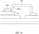
- the conventional semiconductor device has a launch portion GC1 in which one end of a gate clip GC connected to the gate pad TG of the semiconductor element is launched downward, and a bent portion GC2.
- solder material is pressed by the punched portion GC1 and the bent portion GC2. For this reason, when the clearance is not sufficient, the solder material may protrude from the upper surface of the gate pad TG.
- the punched portion GC1 and the bent portion GC2 require at least two steps of a stamping step and a bending step, and the manufacturing cost is increased.
- the conductive joining material cannot be prevented from protruding from the upper surface of the terminal, at the time of joining the terminal and the connector, corresponding to the shape of the terminal (the gate pad) to which the control signal is input, the connection portion of the connector (the gate pad) connected to the terminal is easily processed.
- an object of the present invention is to provide a semiconductor device capable of suppressing the conductive bonding material from protruding from the upper surface of the terminal when the terminal and the connector are bonded, and the joint portion of the connector connected to the terminal is easily processed, corresponding to the shape of the terminal to which the control signal is input.
- a semiconductor device includes: a substrate provided with a first conductive layer and a second conductive layer on an upper surface of the substrate; a semiconductor element disposed on the upper surface of the substrate, the semiconductor element having: a first terminal provided on a lower surface of the semiconductor element and electrically connected to the first conductive layer, and a second terminal provided on an upper surface of the semiconductor element and the second terminal receiving a control signal; a sealing portion that seals the substrate and the semiconductor element; a lead frame that has one end in contact with a upper surface of the second conductive layer provided at an end of the upper surface of the substrate in the sealing portion, and that has the other end exposed from the sealing portion; a first control conductive bonding material bonds between the second conductive layer and the one end of the lead frame at the end of the substrate, and has electrical conductivity; a connector has a one end portion contacting the upper surface of the second terminal of the semiconductor element in the sealing portion, and the other end in contact with the second conductive layer, the connector electrically connecting the second conductive layer
- a thickness of the connector is thinner than a thickness of the lead frame.
- the connector further includes a reference portion connected to the horizontal portion on the side opposite to the first inclined portion, and the reference portion having a width larger than the width of a horizontal portion.
- a height of the lower surface of the control bending portion of the connector from the substrate is higher than a height of the lower surface of the tip portion from the substrate.
- the second control conductive bonding material is arranged along the bending axis direction in which the control bending portion of the connector is in line contact with the upper surface of the second terminal, and the second control conductive bonding material joins between the upper surface of the second terminal and the lower surface side of the control bending portion.
- the upper surface of the second terminal has a rectangular shape
- the second control conductive bonding material is positioned so as to surround the center of the upper surface of the second terminal, and the second control conductive bonding material joins between the lower surface of the control bending portion of the connector and the upper surface of the second terminal.
- the lower surface side of the control bending portion is in line contact with and the upper surface of the second terminal in the bending axis direction passing through the center of the upper surface of the second terminal, and wherein the bending axis direction is parallel to one side of the rectangle of the second terminal.
- a width of the control bending portion in the bending axis direction is the same as a width of the first inclined portion in the bending axis direction.
- a width of the control bending portion in the bending axis direction is smaller than a width of the reference portion in the bending axis direction.
- the semiconductor element is a MOSFET having the first terminal that is a drain terminal, the second terminal that is a gate terminal, and a source terminal which is a third terminal on the upper surface of the MOSFET, the third terminal having an area larger than an area of the second terminal, and wherein the lead frame is a control lead frame for transmitting the gate signal of the MOSFET.
- the semiconductor further comprising:
- a method of manufacturing a semiconductor device according to an aspect of the present invention includes:
- a semiconductor device includes: a substrate provided with a first conductive layer and a second conductive layer on an upper surface of the substrate; a semiconductor element disposed on the upper surface of the substrate, the semiconductor element having: a first terminal provided on a lower surface of the semiconductor element and electrically connected to the first conductive layer, and a second terminal provided on an upper surface of the semiconductor element and the second terminal receiving a control signal; a sealing portion that seals the substrate and the semiconductor element; a lead frame that has one end in contact with a upper surface of the second conductive layer provided at an end of the upper surface of the substrate in the sealing portion, and that has the other end exposed from the sealing portion; a first control conductive bonding material bonds between the second conductive layer and the one end of the lead frame at the end of the substrate, and has electrical conductivity; a connector has a one end portion contacting the upper surface of the second terminal of the semiconductor element in the sealing portion, and the other end in contact with the second conductive layer, the connector electrically connecting the second conductive layer
- the one end portion of the connector comprising: a horizontal portion; a first inclined portion that is connected to the horizontal portion and is located closer to the tip end side of the one end than the horizontal portion, and the first inclined portion having a shape inclined downward from the horizontal portion; and a control bending portion that is connected to the first inclined portion and positioned at the tip of the one end portion, and the control bending portion bent downwardly along the bending axis direction. Furthermore, a lower surface of the control bending portion is in contact with an upper surface of the second terminal.
- control bending portion and the first inclined portion of the connector joined to the second terminal can be formed only by bending.
- the lower surface side of the control bending portion is brought into line contact with the center of the upper surface of the second terminal. Accordingly, a space, for preventing the second control conductive bonding material from protruding from the second terminal when the connector is mounted, can be provided between the first inclined portion and the first inclined portion. Thus, the area of the second terminal can be reduced.
- the semiconductor device of the present invention it is possible to easily process the joint portion of the connector connected to the terminal corresponding to the shape of the terminal to which the control signal is input. Furthermore, it is possible to suppress the conductive bonding material from protruding from the upper surface of the terminal when the terminal and the connector are bonded.
- FIG. 1 is a perspective view showing an example of a configuration of a semiconductor device 100 before sealing.
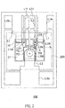
- FIG. 2 is a top view showing an example of the configuration of the semiconductor device 100 after sealing and before cutting the lead frame.
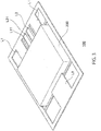
- FIG. 3 is a perspective view showing an example of the configuration of the semiconductor device 100 after sealing and before cutting the lead frame.
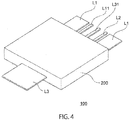
- FIG. 4 is a perspective view showing an example of the configuration of the semiconductor device 100 after the lead frame is cut.
- a case where there are two first lead frames L1 is shown.
- the example of FIG. 2 is illustrated as if the sealing member was transmitted.
- FIG. 5A is an enlarged perspective view of a region in the vicinity of the first and second lead frames L1, L2 and the connector X of the semiconductor device 100 shown in FIG. 1 .
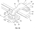
- FIG. 5B is a perspective view further enlarging a region in the vicinity of the connector X shown in FIG. 5A .
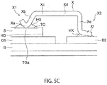
- FIG. 5C is a side view showing an example of a side surface of a region in the vicinity of the connector X shown in FIG. 5B .
- the semiconductor device 100 includes a substrate B, a semiconductor element S, a sealing portion 200, a first lead frame (a drain lead frame) L1, a detection lead frame. L11, a first conductive bonding material H1, a drain conductive bonding material HD, a second lead frame (control lead frame) L2, a second conductive bonding material (a first control conductive bonding material) H2, a second control conductive bonding material HG, a third control conductive bonding material HX, a connector X, a third lead frame (a source lead frame) L3, a source conductive bonding material HS, and a detection lead frame L31 .
- the substrate B is provided with a plurality of conductive layers (a first conductive layer D1 and a second conductive layer D2) on the upper surface of the substrate B.
- the semiconductor element S is arranged on the upper surface of the substrate B.
- the first terminal TD on the lower surface side of the semiconductor element S is electrically connected to the first conductive layer D1 provided on the upper surface of the substrate B.
- the semiconductor element S includes a first terminal (a drain terminal) TD, a second terminal (a gate terminal) TG, and a third terminal (a source terminal) TS.
- the first terminal TD is provided on the lower surface of the semiconductor element S, and is electrically connected to the first conductive layer D1.
- the second terminal TG is provided on the upper surface of the semiconductor element S, and a control signal (a gate signal) is input to the second terminal TG.
- the semiconductor element S is, for example, a MOSFET.
- the semiconductor element S is a MOSFET having a first terminal TD which is a drain terminal is provided on a lower surface of the MOSFET, a second terminal TG which is a gate terminal is provided on the upper surface of the MOSFET, and a third terminal TS which is a source terminal on the upper surface of the MOSFET.
- the semiconductor element S may be other semiconductor elements such as IGBT other than MOSFET.
- the first lead frame L1 has one end L1M electrically connected to the first terminal TD which is a drain terminal in the sealing portion 200, and has the other end L1N exposed from the sealing portion 200.
- the one end portion L1M of the first lead frame L1 is in contact with the upper surface of the first conductive layer D1 at the end extending in the side direction A1 of the upper surface of the substrate B in the sealing portion 200. And, the other end portion L1N of the first lead frame L1 is exposed from the sealing portion 200.
- the one end portion L1M of the first lead frame L1 includes a first arch portion L1b and a first bent portion L1a.
- the first arch portion L1b is provided so as to protrude upward along the reference direction A2.
- first bending portion L1a is connected with the first arch portion L1b, and is located in the tip end side rather than the first arch portion L1b. Furthermore, the first bent portion L1a is bent so as to protrude downward along the reference direction A2.
- the lower surface side of the first bent portion L1a is in line contact with the upper surface of the first conductive layer D12 along the reference direction A2.
- first conductive bonding material H1 bonds between the upper surface of the first conductive layer D1 and the lower surface side of the one end L1M of the first lead frame L1 at the end of the substrate B. Furthermore, the first conductive bonding material H1 has electrical conductivity.
- the first conductive bonding material H1 is, for example, a solder material.
- one end of the detection lead frame L11 is electrically connected to the first terminal TD which is a drain terminal in the sealing unit 200. Furthermore, the other end portion of the detection lead frame L11 is exposed from the sealing portion 200.
- the detection lead frame L11 is for detecting the drain voltage of the semiconductor element S, for example.
- the detection conductive bonding material H11 bonds the first conductive layer D1 and one end portion of the detection lead frame L11. Further, the detection conductive bonding material H11 has electrical conductivity.
- the conductive bonding material for detection H11 is, for example, a solder material.
- one end portion L2M of the second lead frame L2 is in contact with the upper surface of the second conductive layer provided at the end of the upper surface of the substrate B in the sealing portion 200. Further, the other end portion L2N of the second lead frame L2 is exposed from the sealing portion 200.
- the second lead frame L2 is a control lead frame for transmitting the gate signal of the MOSFET (the semiconductor element S) described above.
- the second conductive bonding material (the first control conductive bonding material) H2 bonds between the first conductive layer D1 and the one end L2M of the second lead frame L2 at the end of the substrate B. Further, the second conductive bonding material (the first control conductive bonding material) H2 has electrical conductivity.
- the second conductive bonding material H2 is, for example, a solder material.
- the one end portion L2M of the second lead frame L2 includes a second arch portion L2b and a second bent portion L2a.
- the second arch portion L2b is provided so as to protrude upward along the reference direction A2.
- the second bent portion L2a is connected to the second arch portion L2b and is located on the tip side with respect to the second arch portion L2b.
- the second bent portion L2a is bent so as to protrude downward along the reference direction A2.
- the lower side of the second bent portion L2a is in line contact with the upper surface of the second conductive layer D2 along the reference direction A2.
- the width in the reference direction A2 of the one end portion L1M of the first lead frame L1 is set to be larger than the width in the reference direction A2 of the one end portion L2M of the second lead frame L2.
- one end L3M of the third lead frame L3 is electrically connected to the third terminal TS which is the source terminal on the upper surface of the semiconductor element S. Furthermore, the other end L3N of the third lead frame L3 is exposed from the sealing portion 200.
- the source conductive bonding material HS bonds between the third terminal TS and the one end L3M of the third lead frame L3. Further, the source conductive bonding material HS has electrical conductivity.
- the source conductive bonding material HS is, for example, a solder material.
- the one end of the detection lead frame L31 is electrically connected to the third terminal TS that is the source terminal on the upper surface of the semiconductor element S (that is, the one end of the detection lead frame L31 extends from the third lead frame L3). Further, the other end portion of the detection lead frame L31 is exposed from the sealing portion 200.
- the detection lead frame L31 is for detecting the voltage of the source of the semiconductor element S, for example.
- the sealing portion 200 is configured to seal the substrate B and the semiconductor element S.
- the area of the source terminal, that is the third terminal TS on the upper surface of the semiconductor element S, is larger than the area of the second terminal TG that is the gate terminal.
- the connector X is electrically connected between the second conductive layer D2 and the second terminal (gate terminal) TG on the upper surface side of the semiconductor element S, as shown in FIGS. 5A , 5B and 5C , for example.
- the connector X has one end X1 in contact with the upper surface of the second terminal TG of the semiconductor element S in the sealing portion 200, and has the other end X2 in contact with the second conductive layer D2.
- the second control conductive bonding material HG bonds between the upper surface of the second terminal TG of the semiconductor element S and the one end portion X1 of the connector X. Further, the second control conductive bonding material HG has electrical conductivity.
- the second control conductive bonding material HG is, for example, a solder material.
- the third control conductive bonding material HX bonds between the second conductive layer D2 of the substrate B and the other end X2 of the connector X. Furthermore, the third control conductive bonding material HX has conductivity.
- the third control conductive bonding material HX is, for example, a solder material.
- the connector X is configured to electrically connect the second conductive layer D2 and the second terminal (gate terminal) TG on the upper surface side of the semiconductor element S, by the second and third control conductive bonding materials HG and HX,
- the one end X1 of the connector X includes, for example, a horizontal portion Xc, a first inclined portion Xb, a control bending portion Xa, and a reference portion Xd, as shown in FIGS. 5B and 5C .
- the horizontal portion Xc is arranged in parallel with the upper surface of the substrate B, for example, as shown in FIGS. 5A , 5B , and 5C .
- the first inclined portion Xb is connected to the horizontal portion Xc, and is located closer to the tip end side of the one end portion X1 than the horizontal portion Xc. Furthermore, the first inclined portion Xb has a shape inclined downward from the horizontal portion Xc.
- control bending portion Xa is connected to the first inclined portion Xb and located at the tip of the one end portion X1. Further, the control bending portion Xa is bent so as to protrude downward along the bending axis direction A3.
- the lower surface of the control bending portion Xa is in contact with the upper surface of the second terminal TG.
- the lower surface side of the control bending portion Xa is in contact with the center TGa of the upper surface of the second terminal TG.
- control bending portion Xa is in line contact with the upper surface of the second terminal TG in the bending axis direction A3, for example, as shown in FIG. 5C .
- the width of the control bending portion Xa in the bending axis direction A3 is the same as the width of the first inclined portion Xb in the bending axis direction A3.
- the reference portion Xd is connected to the horizontal portion Xc on the side opposite to the first inclined portion Xb, and has a width larger than the width of the horizontal portion Xc.
- the width of the bending portion for control Xa in the bending axis direction A3 is set to be narrower than the width of the bending portion in the bending axis direction A3 of the reference portion Xd.
- the second control conductive bonding material HG is arranged, along the bending axis direction A3 where the control bending portion Xa of the connector X makes line contact with the upper surface of the second terminal TG, for example, as shown in FIGS. 5A , 5B , and 5C . Furthermore, the second control conductive bonding material HG bonds the upper surface of the second terminal TG and the lower surface side of the control bent portion Xa.
- the upper surface of the second terminal TG has a rectangular shape, for example, as shown in FIGS. 5A , 5B , and 5C .
- the second control conductive bonding material HG is positioned so as to surround the center TGa on the upper surface of the second terminal TG, as shown in FIG. 5B .
- the second control conductive bonding material HG bonds the lower surface of the control bending portion Xa of the connector X and the upper surface of the second terminal TG.
- the lower surface side of the control bending portion Xa of the connector X and the upper surface of the second terminal TG are in line contact with the bending axis direction A3 passing through the center TGa on the upper surface of the second terminal TG.
- the bending axis direction A3 is parallel to one side of the rectangle of the second terminal TG as shown in FIGS. 5A , 5B , and 5C , for example.
- the other end portion X2 of the connector X includes a second inclined portion Xe and a tip end portion Xf.
- the second inclined portion Xe is connected to the reference portion Xd on the side opposite to the horizontal portion Xc, and is located closer to the tip end side of the other end portion X2 than the reference portion Xd. Furthermore, the second inclined portion Xe has a shape inclined downward from the reference portion Xd.
- the tip end portion Xf is connected to the second inclined portion Xe, and the tip end portion Xf is located at the tip of the other end X2, as shown in FIGS. 5A , 5B , and 5C , for example.
- the tip portion Xf is bonded to the upper surface of the second conductive layer D2 of the substrate B, by the third control conductive bonding material HX.
- the height of the lower surface of the control bending portion Xa of the connector X from the upper surface of the substrate B is set to be higher than the height of the lower surface of the tip end portion Xf from the upper surface of the substrate B.
- the thickness in the vertical direction of the connector X is set to be thinner than the thickness in the vertical direction of the second lead frame L2.
- FIG. 6 is an enlarged perspective view of a region in the vicinity of the first lead frame L1 and the detection lead frame L11 of the semiconductor device 100 shown in FIG. 1 .
- FIG. 7 is a perspective view showing an example of the configuration of the first lead frame L1 and the first conductive bonding material H1 shown in FIG. 6 .
- FIG. 8A is a top view showing an example of the configuration of the first lead frame L1 and the first conductive bonding material H1 shown in FIG. 7 .
- FIG. 8B is a cross sectional view showing an example of the configuration of the first lead frame L1 shown in FIG. 8A .
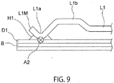
- FIG. 9 is a cross sectional view showing an example of a configuration in the vicinity of one end L1M of the first lead frame L1 shown in FIG. 6 .
- one end portion L1M of the first lead frame L1 includes a first arch portion L1b and a first bent portion L1a.
- the first arch portion L1b is provided so as to protrude upward along the reference direction A2.
- the lower surface side of the first bent portion L1a of the first lead frame L1 is in line contact with the upper surface of the first conductive layer D1 along the reference direction A2.
- the first conductive bonding material H1 is arranged along the reference direction A2 in which the first bent portion L1a of the first lead frame L1 is in line contact with the upper surface of the first conductive layer D1.
- the first conductive bonding material H1 bonds between the upper surface of the first conductive layer D1 and the lower surface side of the first bent portion L1a at the end of the substrate B.
- notch potions L1k are formed on the side surfaces on both sides in the reference direction A2 of the portion, in line contact with the first conductive layer D1, of the first bent portion L1a of the first lead frame L1.
- the notch portions L1k are recessed in the reference direction A2.
- first conductive bonding material H1 is embedded in the notch L1k.
- the part of first electroconductive joining material H1 has joined between the upper surface of the first conductive layer D1 and the notch portions L1k of the first bending portion L1a.
- the first lead frame L1 is arranged, so that the side direction A1, in which the end of the substrate B extends, and the reference direction A2, in which the line contact region of the first bent portion L1a extends, are parallel to each other, for example, as shown in FIGS. 6 to 9 .
- the first lead frame L1 has a main body portion that is located between the one end portion L1M and the other end portion L1N, and the main body portion is sealed in the sealing portion 200. And, the position of the upper surface of the first arch portion L1b is higher than the position of the upper surface of the said main body portion.
- the width in the side direction A1 of the first arch portion L1b is the same as the width in the side direction A1 other than the cutout portion L1k of the first bent portion L1a. That is, the width in the side direction A1 of the first arch portion L1b is larger than the width in the side direction A1 of the cutout portion L1k of the first bent portion L1a.
- the one end L1M and the other end L1N of the first lead frame L1 have the same thickness (that is, the first lead frame L1 is not coined).
- the position of the lower surface of the first bent portion L1a is set to be lower than the position of the lower surface of the main body portion.
- the first arch portion L1b releases the stress applied to the first lead frame L1 to the sealing portion 200 in the periphery.
- application of stress to the first bent portion L1a of the first lead frame L1 is suppressed.
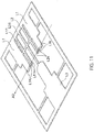
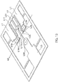
- FIGS. 10 to 13 are diagrams illustrating an example of a process of a method of manufacturing the semiconductor device 100.
- a metal plate 300 made of a metal such as copper is prepared.
- the first to third lead frames L1 to L3 are simultaneously formed.
- notches L1k are formed on both side surfaces in the reference direction A2 of the portion, where the first bent portion L1a of the first lead frame L1 is formed, that is in line contact with the first conductive layer D1.
- the notches L1k are recessed in the reference direction A2.
- notch portions L2k are formed on both side surfaces in the reference direction A2 of the portion, where the second bent portion L2a of the second lead frame L2 is formed, that is in line contact with the second conductive layer D2.
- the notch portions L2k are recessed in the reference direction A2.
- the one end of the first and second lead frame L1, L2 are bent so as to protrude downward along the reference direction A2. Thereby, the first and second bending portion L1a, L2a are formed.
- the third lead frame L3 is subjected to predetermined processing to form a predetermined shape L3X.
- the first to third lead frames L1 to L3 shown in FIG. 1 are formed.
- a substrate B having a first conductive layer D1 and a second conductive layer D2 provided on the upper surface is prepared.
- the semiconductor element S is arranged on the upper surface of the substrate B.
- the semiconductor element S has a first terminal TD provided on the lower surface and electrically connected to the first conductive layer D1, and has a second terminal TG provided on the upper surface and to which a control signal is input. Then, by joining the first terminal TD to the first conductive layer D1, the first conductive layer D1 and the first terminal TD are electrically connected.
- one end of the first lead frame L1 is brought into contact with the upper surface of the first conductive layer D1 provided at the end of the upper surface of the substrate B. Then, the upper surface of the first conductive layer and the lower surface side of the first bent portion of the first lead frame L1 are joined at the end of the substrate B, with the first conductive bonding material H1. Further, a part of the first conductive bonding material H1 is embedded in the notch portions L1k. Thereby, the upper surface of the first conductive layer D1 and the notch portions L1k of the first bent portion L1a are joined.
- one end of the second lead frame L2 is brought into contact with the upper surface of the second conductive layer D2 provided at the end of the upper surface of the substrate B. Then, at the end of the substrate B, the second conductive layer D2 and one end of the second lead frame L2 are joined by the first control conductive bonding material H2 having electrical conductivity ( FIG. 1 ). At this time, a part of the second conductive bonding material H2 is embedded in the notch L2k. Thereby, the upper surface of the second conductive layer D2 and the cutout portion L2k of the second bent portion L2a are joined.
- the one end portion of the third lead frame L3 is brought into contact with the upper surface of the third terminal TS on the upper surface of the semiconductor element S. Then, the third terminal TS and the one end portion of the third lead frame L3 are joined by the source conductive joint material HS having electrical conductivity ( FIG. 1 ).
- one end X1 of the connector X is brought into contact with the upper surface of the second terminal TG of the semiconductor element S. Further, the other end X2 of the connector X is brought into contact with the second conductive layer D2. Further, the upper surface of the second terminal of the semiconductor element S and the one end portion X1 of the connector X are bonded by the second control conductive bonding material HG having electrical conductivity. Furthermore, the second conductive layer D2 of the substrate B and the other end portion X2 of the connector X are joined by the third conductive control material HX having electrical conductivity.
- the substrate B, the semiconductor element S, the connector X, the first to third lead frames L1 to L3, and the one end of detection lead frames L11 and L31 are sealed by the sealing portion 200.
- the semiconductor device 100 shown in FIG. 4 is manufactured.
- the first and second lead frames L1 and L2 can be formed by two steps of bending the one end of the first and second lead frames L1 and L2. For this reason, the processing cost is reduced, and the thickness of the solder is ensured at the outer peripheral portion of the joint portion, so that stress relaxation is possible.
- the first and second bent portions L1a and L2a can be easily bent. Furthermore, since the solder flows into the notch portions L1k and I2k, the fixing by the solder can be ensured.
- the tip of the first and second lead frames L1 and L2 are bent by bending.
- the bent first and second bent portions L1a and L2a are connected to the first and second conductive layers D1 and D2 by the line contact. For this reason, it is possible to reduce the amount of solder material dispensed.
- the semiconductor device includes: a substrate B provided with a first conductive layer D1 and a second conductive layer D2 on an upper surface of the substrate; a semiconductor element S disposed on the upper surface of the substrate, the semiconductor element having: a first terminal provided on a lower surface of the semiconductor element and electrically connected to the first conductive layer, and a second terminal provided on an upper surface of the semiconductor element and the second terminal receiving a control signal; a sealing portion that seals the substrate and the semiconductor element; a control lead frame that has one end in contact with a upper surface of the second conductive layer D2 provided at an end of the upper surface of the substrate in the sealing portion, and that has the other end exposed from the sealing portion; a first control conductive bonding material H2 bonds between the second conductive layer and the one end of the control lead frame at the end of the substrate, and has electrical conductivity; a connector X has a one end portion contacting the upper surface of the second terminal of the semiconductor element in the sealing portion, and the other end in contact with
- the one end portion of the connector includes: a horizontal portion Xc; a first inclined portion Xb that is connected to the horizontal portion and is located closer to the tip end side of the one end than the horizontal portion, and the first inclined portion having a shape inclined downward from the horizontal portion; and a control bending portion Xa that is connected to the first inclined portion and positioned at the tip of the one end portion, and the control bending portion bent downwardly along the bending axis direction, and wherein a lower surface of the control bending portion Xa is in contact with an upper surface of the second terminal.
- control bent portion Xa and the first inclined portion Xb of the connector X joined to the second terminal (gate pad) T2 can be formed only by bending.
- the lower surface side of the control bent portion Xa is brought into line contact with the center of the upper surface of the second terminal.
- a space for preventing the second control conductive bonding material (solder material) H2 from protruding from the second terminal can be provided between the first inclined portion Xb.
- the area of the second terminal can be reduced.
- the semiconductor device of the present invention it is possible to easily process the joint portion of the connector connected to the terminal corresponding to the shape of the terminal to which the control signal is input. Furthermore, it is possible to suppress the conductive bonding material from protruding from the upper surface of the terminal, when the terminal and the connector are bonded.
Landscapes
- Lead Frames For Integrated Circuits (AREA)
Abstract
Description
- The present invention relates to a semiconductor device and a method of manufacturing the semiconductor device.
- Conventionally, for example, a semiconductor device in which a semiconductor element is placed on a conductor layer of a substrate is known (see Patent Document 1). In this semiconductor device, the semiconductor element and the lead frame are joined with a connector via a conductive joining material such as solder, and the semiconductor element and the substrate are sealed with a sealing resin.
- In such a conventional semiconductor device, for example, in order to connect a connector such as a gate clip and a semiconductor element (such as a MOSFET or 1GBT), a conductive bonding material such as a solder material may be applied. In this case, there is a limit to reducing the amount of solder while maintaining the solder particle size, and the cost increases as the solder particle size decreases.
- And, in order to suppress the solder bridge between different electrodes without reducing the amount of solder, it is necessary to prevent the solder material that contacts the connector from protruding from the upper surface of the gate pad (the terminal) to which the control signal of the semiconductor element is input.
- In consideration of electrical characteristics, it is necessary to reduce the area of the gate pad and increase the area of the source pad. For this reason, it is necessary to make the junction between the gate clip and the gate pad as small as possible.
- Here, for example, as shown in
FIG. 14 , the conventional semiconductor device has a launch portion GC1 in which one end of a gate clip GC connected to the gate pad TG of the semiconductor element is launched downward, and a bent portion GC2. - The solder material is pressed by the punched portion GC1 and the bent portion GC2. For this reason, when the clearance is not sufficient, the solder material may protrude from the upper surface of the gate pad TG.
- Therefore, it is necessary to expand the area of the gate pad TG (
FIG. 14 ). In addition, the punched portion GC1 and the bent portion GC2 require at least two steps of a stamping step and a bending step, and the manufacturing cost is increased. - Thus, in the conventional semiconductor device, there is a problem that the conductive joining material cannot be prevented from protruding from the upper surface of the terminal, at the time of joining the terminal and the connector, corresponding to the shape of the terminal (the gate pad) to which the control signal is input, the connection portion of the connector (the gate pad) connected to the terminal is easily processed.
- [Patent Document 1]
JP2015-12065 - Therefore, an object of the present invention is to provide a semiconductor device capable of suppressing the conductive bonding material from protruding from the upper surface of the terminal when the terminal and the connector are bonded, and the joint portion of the connector connected to the terminal is easily processed, corresponding to the shape of the terminal to which the control signal is input.
- A semiconductor device according to an aspect of the present invention includes: a substrate provided with a first conductive layer and a second conductive layer on an upper surface of the substrate;
a semiconductor element disposed on the upper surface of the substrate, the semiconductor element having: a first terminal provided on a lower surface of the semiconductor element and electrically connected to the first conductive layer, and a second terminal provided on an upper surface of the semiconductor element and the second terminal receiving a control signal;
a sealing portion that seals the substrate and the semiconductor element;
a lead frame that has one end in contact with a upper surface of the second conductive layer provided at an end of the upper surface of the substrate in the sealing portion, and that has the other end exposed from the sealing portion;
a first control conductive bonding material bonds between the second conductive layer and the one end of the lead frame at the end of the substrate, and has electrical conductivity;
a connector has a one end portion contacting the upper surface of the second terminal of the semiconductor element in the sealing portion, and the other end in contact with the second conductive layer, the connector electrically connecting the second conductive layer and the second terminal on the upper surface of the semiconductor element;
a second control conductive bonding material bonds between the upper surface of the second terminal of the semiconductor element and the one end of the connector, and has electrical conductivity; and
a third control conductive bonding material bonds the second conductive layer of the substrate and the other end of the connector, and has electrical conductivity,
wherein the one end portion of the connector comprising: - a horizontal portion;
- a first inclined portion that is connected to the horizontal portion and is located closer to the tip end side of the one end than the horizontal portion, and the first inclined portion having a shape inclined downward from the horizontal portion; and
- a control bending portion that is connected to the first inclined portion and positioned at the tip of the one end portion, and the control bending portion bent downwardly along the bending axis direction, and wherein a lower surface of the control bending portion is in contact with an upper surface of the second terminal.
- In the semiconductor device,
wherein a lower surface side of the control bending portion is in contact with a center of an upper surface of the second terminal. - In the semiconductor device,
wherein the lower surface side of the control bending portion is in line contact with the upper surface of the second terminal in the bending axis direction. - In the semiconductor device,
wherein a thickness of the connector is thinner than a thickness of the lead frame. - In the semiconductor device,
wherein the connector further includes a reference portion connected to the horizontal portion on the side opposite to the first inclined portion, and the reference portion having a width larger than the width of a horizontal portion. - In the semiconductor device,
wherein the other end of the connector has: - a second inclined portion that is connected to the reference portion on the side opposite to the horizontal portion, and that is located closer to the tip end side of the other end portion than the reference portion, the second inclined portion having a shape inclined downward from the reference portion, and
- a tip portion that is connected to the second inclined portion, and is located at a tip of the other end portion of the connector,
- In the semiconductor device,
wherein a height of the lower surface of the control bending portion of the connector from the substrate is higher than a height of the lower surface of the tip portion from the substrate. - In the semiconductor device,
wherein the second control conductive bonding material is arranged along the bending axis direction in which the control bending portion of the connector is in line contact with the upper surface of the second terminal, and the second control conductive bonding material joins between the upper surface of the second terminal and the lower surface side of the control bending portion. - In the semiconductor device,
wherein the upper surface of the second terminal has a rectangular shape, and
wherein the second control conductive bonding material is positioned so as to surround the center of the upper surface of the second terminal, and the second control conductive bonding material joins between the lower surface of the control bending portion of the connector and the upper surface of the second terminal. - In the semiconductor device,
wherein the lower surface side of the control bending portion is in line contact with and the upper surface of the second terminal in the bending axis direction passing through the center of the upper surface of the second terminal, and
wherein the bending axis direction is parallel to one side of the rectangle of the second terminal. - In the semiconductor device,
wherein a width of the control bending portion in the bending axis direction is the same as a width of the first inclined portion in the bending axis direction. - In the semiconductor device,
wherein a width of the control bending portion in the bending axis direction is smaller than a width of the reference portion in the bending axis direction. - In the semiconductor device,
wherein the semiconductor element is a MOSFET having the first terminal that is a drain terminal, the second terminal that is a gate terminal, and a source terminal which is a third terminal on the upper surface of the MOSFET, the third terminal having an area larger than an area of the second terminal, and
wherein the lead frame is a control lead frame for transmitting the gate signal of the MOSFET. - In the semiconductor device,
the semiconductor further comprising: - a drain lead frame having one end electrically connected to the first terminal, which is a drain terminal in the sealing portion, and having the other end exposed from the sealing portion; and
- a source lead frame having one end electrically connected to the third terminal, which is a source terminal in the sealing portion, and having the other end exposed from the sealing portion.
- A method of manufacturing a semiconductor device according to an aspect of the present invention includes:
- preparing a substrate provided with a first conductive layer and a second conductive layer on an upper surface of the substrate;
- arranging a semiconductor element on the upper surface of the substrate, the semiconductor element having: a first terminal provided on a lower surface of the semiconductor element and electrically connected to the first conductive layer, and a second terminal provided on an upper surface of the semiconductor element and the second terminal receiving a control signal;
- bringing one end of a lead frame into contact with a upper surface of the second conductive layer provided at an end of the upper surface of the substrate;
- bonding between the second conductive layer and the one end of the lead frame at the end of the substrate by a first control conductive bonding material, and the first control conductive bonding material has electrical conductivity;
- bringing a one end portion of a connector into contact with the upper surface of the second terminal of the semiconductor element, and the other end of a connector into contact with the second conductive layer;
- bonding between the upper surface of the second terminal of the semiconductor element and the one end of the connector by a second control conductive bonding material, and the second control conductive bonding material has electrical conductivity;
- bonding the second conductive layer of the substrate and the other end of the connector by a third control conductive bonding material, and the third control conductive bonding material has electrical conductivity; and
- sealing the substrate, the semiconductor element, and the one end of the lead frame by a sealing portion,
- a horizontal portion;
- a first inclined portion that is connected to the horizontal portion and is located closer to the tip end side of the one end than the horizontal portion, and the first inclined portion having a shape inclined downward from the horizontal portion; and
- a control bending portion that is connected to the first inclined portion and positioned at the tip of the one end portion, and the control bending portion bent downwardly along the bending axis direction, and
- A semiconductor device according to an aspect of the present invention includes: a substrate provided with a first conductive layer and a second conductive layer on an upper surface of the substrate; a semiconductor element disposed on the upper surface of the substrate, the semiconductor element having: a first terminal provided on a lower surface of the semiconductor element and electrically connected to the first conductive layer, and a second terminal provided on an upper surface of the semiconductor element and the second terminal receiving a control signal; a sealing portion that seals the substrate and the semiconductor element; a lead frame that has one end in contact with a upper surface of the second conductive layer provided at an end of the upper surface of the substrate in the sealing portion, and that has the other end exposed from the sealing portion; a first control conductive bonding material bonds between the second conductive layer and the one end of the lead frame at the end of the substrate, and has electrical conductivity; a connector has a one end portion contacting the upper surface of the second terminal of the semiconductor element in the sealing portion, and the other end in contact with the second conductive layer, the connector electrically connecting the second conductive layer and the second terminal on the upper surface of the semiconductor element; a second control conductive bonding material bonds between the upper surface of the second terminal of the semiconductor element and the one end of the connector, and has electrical conductivity; and a third control conductive bonding material bonds the second conductive layer of the substrate and the other end of the connector, and has electrical conductivity.
- Furthermore, the one end portion of the connector comprising: a horizontal portion; a first inclined portion that is connected to the horizontal portion and is located closer to the tip end side of the one end than the horizontal portion, and the first inclined portion having a shape inclined downward from the horizontal portion; and a control bending portion that is connected to the first inclined portion and positioned at the tip of the one end portion, and the control bending portion bent downwardly along the bending axis direction. Furthermore, a lower surface of the control bending portion is in contact with an upper surface of the second terminal.
- In the semiconductor device of the present invention, for example, the control bending portion and the first inclined portion of the connector joined to the second terminal can be formed only by bending.
- Especially, the lower surface side of the control bending portion is brought into line contact with the center of the upper surface of the second terminal. Accordingly, a space, for preventing the second control conductive bonding material from protruding from the second terminal when the connector is mounted, can be provided between the first inclined portion and the first inclined portion. Thus, the area of the second terminal can be reduced.
- That is, in the semiconductor device of the present invention, it is possible to easily process the joint portion of the connector connected to the terminal corresponding to the shape of the terminal to which the control signal is input. Furthermore, it is possible to suppress the conductive bonding material from protruding from the upper surface of the terminal when the terminal and the connector are bonded.
-
- [
FIG.1] FIG. 1 is a perspective view showing an example of a configuration of asemiconductor device 100 before sealing. - [
FIG.2] FIG. 2 is a top view showing an example of the configuration of thesemiconductor device 100 after sealing and before cutting the lead frame. - [
FIG.3] FIG. 3 is a perspective view showing an example of the configuration of thesemiconductor device 100 after sealing and before cutting the lead frame. - [
FIG.4] FIG. 4 is a perspective view showing an example of the configuration of thesemiconductor device 100 after the lead frame is cut. - [
FIG.5A] FIG. 5A is an enlarged perspective view of a region in the vicinity of the first and second lead frames L1, L2 and the connector X of thesemiconductor device 100 shown inFIG. 1 . - [
FIG.5B] FIG. 5B is a perspective view further enlarging a region in the vicinity of the connector X shown inFIG. 5A . - [
FIG.5C] FIG. 5C is a side view showing an example of a side surface of a region in the vicinity of the connector X shown inFIG. 5B . - [
FIG.6] FIG. 6 is an enlarged perspective view of a region in the vicinity of the first lead frame L1 and the detection lead frame L11 of thesemiconductor device 100 shown inFIG. 1 . - [
FIG.7] FIG. 7 is a perspective view showing an example of the configuration of the first lead frame L1 and the first conductive bonding material H1 shown inFIG. 6 . - [
FIG.8A] FIG. 8A is a top view showing an example of the configuration of the first lead frame L1 and the first conductive bonding material H1 shown inFIG. 7 . - [FIG.8B] FIG. 8B is a cross-sectional view showing an example of the configuration of the first lead frame L1 shown in
FIG. 8A . - [
FIG.9] FIG. 9 is a cross-sectional view showing an example of the configuration in the vicinity of one end L1M of the first lead frame L1 shown inFIG. 9 . - [
FIG.10] FIG. 10 is a diagram illustrating an example of a process of a method of manufacturing thesemiconductor device 100. - [
FIG.11] FIG. 11 is a diagram illustrating an example of a process of the method of manufacturing thesemiconductor device 100 subsequent toFIG. 10 . - [
FIG.12] FIG. 12 is a diagram illustrating an example of a process of the method of manufacturing thesemiconductor device 100 subsequent toFIG. 11 . - [
FIG.13] FIG. 13 is a diagram illustrating an example of a process of the method of manufacturing thesemiconductor device 100 subsequent toFIG. 12 . - [
FIG.14] FIG. 14 is a cross sectional view showing an example of a configuration of a connector of a conventional semiconductor device. - Embodiments of the present invention will now be described with reference to the accompanying drawings.
-
FIG. 1 is a perspective view showing an example of a configuration of asemiconductor device 100 before sealing.FIG. 2 is a top view showing an example of the configuration of thesemiconductor device 100 after sealing and before cutting the lead frame.FIG. 3 is a perspective view showing an example of the configuration of thesemiconductor device 100 after sealing and before cutting the lead frame.FIG. 4 is a perspective view showing an example of the configuration of thesemiconductor device 100 after the lead frame is cut. In the example ofFIG. 1 , a case where there are two first lead frames L1 is shown. Moreover, the example ofFIG. 2 is illustrated as if the sealing member was transmitted. -
FIG. 5A is an enlarged perspective view of a region in the vicinity of the first and second lead frames L1, L2 and the connector X of thesemiconductor device 100 shown inFIG. 1 .FIG. 5B is a perspective view further enlarging a region in the vicinity of the connector X shown inFIG. 5A .FIG. 5C is a side view showing an example of a side surface of a region in the vicinity of the connector X shown inFIG. 5B . - For example, as shown in
FIGS. 1 to 4 , thesemiconductor device 100 includes a substrate B, a semiconductor element S, a sealingportion 200, a first lead frame (a drain lead frame) L1, a detection lead frame. L11, a first conductive bonding material H1, a drain conductive bonding material HD, a second lead frame (control lead frame) L2, a second conductive bonding material (a first control conductive bonding material) H2, a second control conductive bonding material HG, a third control conductive bonding material HX, a connector X, a third lead frame (a source lead frame) L3, a source conductive bonding material HS, and a detection lead frame L31 . - As shown in
FIGS. 1 and2 , the substrate B is provided with a plurality of conductive layers (a first conductive layer D1 and a second conductive layer D2) on the upper surface of the substrate B. - Also, as shown in
FIGS. 1 and2 , the semiconductor element S is arranged on the upper surface of the substrate B. In the semiconductor element S, the first terminal TD on the lower surface side of the semiconductor element S is electrically connected to the first conductive layer D1 provided on the upper surface of the substrate B. - For example, as shown in
FIGS. 1 and2 , the semiconductor element S includes a first terminal (a drain terminal) TD, a second terminal (a gate terminal) TG, and a third terminal (a source terminal) TS. - The first terminal TD is provided on the lower surface of the semiconductor element S, and is electrically connected to the first conductive layer D1.
- The second terminal TG is provided on the upper surface of the semiconductor element S, and a control signal (a gate signal) is input to the second terminal TG.
- Note that the semiconductor element S is, for example, a MOSFET. In this case, the semiconductor element S is a MOSFET having a first terminal TD which is a drain terminal is provided on a lower surface of the MOSFET, a second terminal TG which is a gate terminal is provided on the upper surface of the MOSFET, and a third terminal TS which is a source terminal on the upper surface of the MOSFET.
- The semiconductor element S may be other semiconductor elements such as IGBT other than MOSFET.
- As shown in
FIGS. 1 and2 , the first lead frame L1 has one end L1M electrically connected to the first terminal TD which is a drain terminal in the sealingportion 200, and has the other end L1N exposed from the sealingportion 200. - In particular, the one end portion L1M of the first lead frame L1 is in contact with the upper surface of the first conductive layer D1 at the end extending in the side direction A1 of the upper surface of the substrate B in the sealing
portion 200. And, the other end portion L1N of the first lead frame L1 is exposed from the sealingportion 200. - The one end portion L1M of the first lead frame L1 includes a first arch portion L1b and a first bent portion L1a.
- The first arch portion L1b is provided so as to protrude upward along the reference direction A2.
- And, the first bending portion L1a is connected with the first arch portion L1b, and is located in the tip end side rather than the first arch portion L1b. Furthermore, the first bent portion L1a is bent so as to protrude downward along the reference direction A2.
- The lower surface side of the first bent portion L1a is in line contact with the upper surface of the first conductive layer D12 along the reference direction A2.
- Further, the first conductive bonding material H1 bonds between the upper surface of the first conductive layer D1 and the lower surface side of the one end L1M of the first lead frame L1 at the end of the substrate B. Furthermore, the first conductive bonding material H1 has electrical conductivity.
- Note that the first conductive bonding material H1 is, for example, a solder material.
- Further, one end of the detection lead frame L11 is electrically connected to the first terminal TD which is a drain terminal in the
sealing unit 200. Furthermore, the other end portion of the detection lead frame L11 is exposed from the sealingportion 200. - The detection lead frame L11 is for detecting the drain voltage of the semiconductor element S, for example.
- Then, the detection conductive bonding material H11 bonds the first conductive layer D1 and one end portion of the detection lead frame L11. Further, the detection conductive bonding material H11 has electrical conductivity.
- Note that the conductive bonding material for detection H11 is, for example, a solder material.
- For example, as shown in
FIGS. 1 and2 , one end portion L2M of the second lead frame L2 is in contact with the upper surface of the second conductive layer provided at the end of the upper surface of the substrate B in the sealingportion 200. Further, the other end portion L2N of the second lead frame L2 is exposed from the sealingportion 200. - The second lead frame L2 is a control lead frame for transmitting the gate signal of the MOSFET (the semiconductor element S) described above.
- Then, the second conductive bonding material (the first control conductive bonding material) H2 bonds between the first conductive layer D1 and the one end L2M of the second lead frame L2 at the end of the substrate B. Further, the second conductive bonding material (the first control conductive bonding material) H2 has electrical conductivity.
- Note that the second conductive bonding material H2 is, for example, a solder material.
- Also, the one end portion L2M of the second lead frame L2 includes a second arch portion L2b and a second bent portion L2a.
- The second arch portion L2b is provided so as to protrude upward along the reference direction A2.
- The second bent portion L2a is connected to the second arch portion L2b and is located on the tip side with respect to the second arch portion L2b. The second bent portion L2a is bent so as to protrude downward along the reference direction A2.
- The lower side of the second bent portion L2a is in line contact with the upper surface of the second conductive layer D2 along the reference direction A2.
- Further, the width in the reference direction A2 of the one end portion L1M of the first lead frame L1 is set to be larger than the width in the reference direction A2 of the one end portion L2M of the second lead frame L2.
- Also, one end L3M of the third lead frame L3 is electrically connected to the third terminal TS which is the source terminal on the upper surface of the semiconductor element S. Furthermore, the other end L3N of the third lead frame L3 is exposed from the sealing
portion 200. - Then, the source conductive bonding material HS bonds between the third terminal TS and the one end L3M of the third lead frame L3. Further, the source conductive bonding material HS has electrical conductivity.
- The source conductive bonding material HS is, for example, a solder material.
- The one end of the detection lead frame L31 is electrically connected to the third terminal TS that is the source terminal on the upper surface of the semiconductor element S (that is, the one end of the detection lead frame L31 extends from the third lead frame L3). Further, the other end portion of the detection lead frame L31 is exposed from the sealing
portion 200. - The detection lead frame L31 is for detecting the voltage of the source of the semiconductor element S, for example.
- Further, as shown in
FIGS. 1 to 4 , the sealingportion 200 is configured to seal the substrate B and the semiconductor element S. - Here, in the example shown in
FIGS. 5A ,5B , and5C , the area of the source terminal, that is the third terminal TS on the upper surface of the semiconductor element S, is larger than the area of the second terminal TG that is the gate terminal. - The connector X is electrically connected between the second conductive layer D2 and the second terminal (gate terminal) TG on the upper surface side of the semiconductor element S, as shown in
FIGS. 5A ,5B and5C , for example. - For example, as shown in
FIGS. 5A ,5B , and5C , the connector X has one end X1 in contact with the upper surface of the second terminal TG of the semiconductor element S in the sealingportion 200, and has the other end X2 in contact with the second conductive layer D2. - Here, the second control conductive bonding material HG bonds between the upper surface of the second terminal TG of the semiconductor element S and the one end portion X1 of the connector X. Further, the second control conductive bonding material HG has electrical conductivity.
- Note that the second control conductive bonding material HG is, for example, a solder material.
- Further, the third control conductive bonding material HX bonds between the second conductive layer D2 of the substrate B and the other end X2 of the connector X. Furthermore, the third control conductive bonding material HX has conductivity.
- Note that the third control conductive bonding material HX is, for example, a solder material.
- That is, the connector X is configured to electrically connect the second conductive layer D2 and the second terminal (gate terminal) TG on the upper surface side of the semiconductor element S, by the second and third control conductive bonding materials HG and HX,
- The one end X1 of the connector X includes, for example, a horizontal portion Xc, a first inclined portion Xb, a control bending portion Xa, and a reference portion Xd, as shown in
FIGS. 5B and5C . - And, the horizontal portion Xc is arranged in parallel with the upper surface of the substrate B, for example, as shown in
FIGS. 5A ,5B , and5C . - Further, for example, as shown in
FIGS. 5A ,5B , and5C , the first inclined portion Xb is connected to the horizontal portion Xc, and is located closer to the tip end side of the one end portion X1 than the horizontal portion Xc. Furthermore, the first inclined portion Xb has a shape inclined downward from the horizontal portion Xc. - Further, for example, as shown in
FIG. 5B , the control bending portion Xa is connected to the first inclined portion Xb and located at the tip of the one end portion X1. Further, the control bending portion Xa is bent so as to protrude downward along the bending axis direction A3. - The lower surface of the control bending portion Xa is in contact with the upper surface of the second terminal TG. In particular, the lower surface side of the control bending portion Xa is in contact with the center TGa of the upper surface of the second terminal TG.
- Further, the lower surface side of the control bending portion Xa is in line contact with the upper surface of the second terminal TG in the bending axis direction A3, for example, as shown in
FIG. 5C . - The width of the control bending portion Xa in the bending axis direction A3 is the same as the width of the first inclined portion Xb in the bending axis direction A3.
- In addition, the reference portion Xd is connected to the horizontal portion Xc on the side opposite to the first inclined portion Xb, and has a width larger than the width of the horizontal portion Xc.
- The width of the bending portion for control Xa in the bending axis direction A3 is set to be narrower than the width of the bending portion in the bending axis direction A3 of the reference portion Xd.
- Here, the second control conductive bonding material HG is arranged, along the bending axis direction A3 where the control bending portion Xa of the connector X makes line contact with the upper surface of the second terminal TG, for example, as shown in
FIGS. 5A ,5B , and5C . Furthermore, the second control conductive bonding material HG bonds the upper surface of the second terminal TG and the lower surface side of the control bent portion Xa. - The upper surface of the second terminal TG has a rectangular shape, for example, as shown in
FIGS. 5A ,5B , and5C . - The second control conductive bonding material HG is positioned so as to surround the center TGa on the upper surface of the second terminal TG, as shown in
FIG. 5B . Thus, the second control conductive bonding material HG bonds the lower surface of the control bending portion Xa of the connector X and the upper surface of the second terminal TG. - For example, as shown in
FIG. 5C , the lower surface side of the control bending portion Xa of the connector X and the upper surface of the second terminal TG are in line contact with the bending axis direction A3 passing through the center TGa on the upper surface of the second terminal TG. - The bending axis direction A3 is parallel to one side of the rectangle of the second terminal TG as shown in
FIGS. 5A ,5B , and5C , for example. - Meanwhile, the other end portion X2 of the connector X includes a second inclined portion Xe and a tip end portion Xf.
- The second inclined portion Xe is connected to the reference portion Xd on the side opposite to the horizontal portion Xc, and is located closer to the tip end side of the other end portion X2 than the reference portion Xd. Furthermore, the second inclined portion Xe has a shape inclined downward from the reference portion Xd.
- And, the tip end portion Xf is connected to the second inclined portion Xe, and the tip end portion Xf is located at the tip of the other end X2, as shown in
FIGS. 5A ,5B , and5C , for example. - The tip portion Xf is bonded to the upper surface of the second conductive layer D2 of the substrate B, by the third control conductive bonding material HX.
- The height of the lower surface of the control bending portion Xa of the connector X from the upper surface of the substrate B is set to be higher than the height of the lower surface of the tip end portion Xf from the upper surface of the substrate B.
- Note that the thickness in the vertical direction of the connector X is set to be thinner than the thickness in the vertical direction of the second lead frame L2.
- Thereby, the bending process of the miniaturized connector X can be facilitated.
-
FIG. 6 is an enlarged perspective view of a region in the vicinity of the first lead frame L1 and the detection lead frame L11 of thesemiconductor device 100 shown inFIG. 1 .FIG. 7 is a perspective view showing an example of the configuration of the first lead frame L1 and the first conductive bonding material H1 shown inFIG. 6 .FIG. 8A is a top view showing an example of the configuration of the first lead frame L1 and the first conductive bonding material H1 shown inFIG. 7 . FIG. 8B is a cross sectional view showing an example of the configuration of the first lead frame L1 shown inFIG. 8A .FIG. 9 is a cross sectional view showing an example of a configuration in the vicinity of one end L1M of the first lead frame L1 shown inFIG. 6 . - For example, as shown in
FIGS. 6 to 9 , one end portion L1M of the first lead frame L1 includes a first arch portion L1b and a first bent portion L1a. - The first arch portion L1b is provided so as to protrude upward along the reference direction A2.
- The lower surface side of the first bent portion L1a of the first lead frame L1 is in line contact with the upper surface of the first conductive layer D1 along the reference direction A2.
- The first conductive bonding material H1 is arranged along the reference direction A2 in which the first bent portion L1a of the first lead frame L1 is in line contact with the upper surface of the first conductive layer D1. The first conductive bonding material H1 bonds between the upper surface of the first conductive layer D1 and the lower surface side of the first bent portion L1a at the end of the substrate B.
- Here, as shown in
FIGS. 6 to 9 , notch potions L1k are formed on the side surfaces on both sides in the reference direction A2 of the portion, in line contact with the first conductive layer D1, of the first bent portion L1a of the first lead frame L1. The notch portions L1k are recessed in the reference direction A2. - And, a part of the first conductive bonding material H1 is embedded in the notch L1k. Thereby, the part of first electroconductive joining material H1 has joined between the upper surface of the first conductive layer D1 and the notch portions L1k of the first bending portion L1a.
- The first lead frame L1 is arranged, so that the side direction A1, in which the end of the substrate B extends, and the reference direction A2, in which the line contact region of the first bent portion L1a extends, are parallel to each other, for example, as shown in
FIGS. 6 to 9 . - The first lead frame L1 has a main body portion that is located between the one end portion L1M and the other end portion L1N, and the main body portion is sealed in the sealing
portion 200. And, the position of the upper surface of the first arch portion L1b is higher than the position of the upper surface of the said main body portion. - The width in the side direction A1 of the first arch portion L1b is the same as the width in the side direction A1 other than the cutout portion L1k of the first bent portion L1a. That is, the width in the side direction A1 of the first arch portion L1b is larger than the width in the side direction A1 of the cutout portion L1k of the first bent portion L1a.
- Further, for example, the one end L1M and the other end L1N of the first lead frame L1 have the same thickness (that is, the first lead frame L1 is not coined).
- Note that the position of the lower surface of the first bent portion L1a is set to be lower than the position of the lower surface of the main body portion.
- Then, the first arch portion L1b releases the stress applied to the first lead frame L1 to the sealing
portion 200 in the periphery. As a result, application of stress to the first bent portion L1a of the first lead frame L1 is suppressed. - In the third example, an example of a method of manufacturing the
semiconductor device 100 having the configuration as described above will be described. -
FIGS. 10 to 13 are diagrams illustrating an example of a process of a method of manufacturing thesemiconductor device 100. - First, as shown in
FIG. 10 , for example, ametal plate 300 made of a metal such as copper is prepared. - Then, as shown in
FIG. 11 , by selectively punching out themetal plate 300, the first to third lead frames L1 to L3 are simultaneously formed. - In particular, when the first lead frame L1 is formed, notches L1k are formed on both side surfaces in the reference direction A2 of the portion, where the first bent portion L1a of the first lead frame L1 is formed, that is in line contact with the first conductive layer D1. The notches L1k are recessed in the reference direction A2.
- In the same way, when the second lead frame L2 is formed, notch portions L2k are formed on both side surfaces in the reference direction A2 of the portion, where the second bent portion L2a of the second lead frame L2 is formed, that is in line contact with the second conductive layer D2. The notch portions L2k are recessed in the reference direction A2.
- Then, as shown in
FIG. 12 , the one end of the first and second lead frame L1, L2 are bent so as to protrude downward along the reference direction A2. Thereby, the first and second bending portion L1a, L2a are formed. - Then, as shown in
FIG. 13 , the third lead frame L3 is subjected to predetermined processing to form a predetermined shape L3X. - Through these steps, for example, the first to third lead frames L1 to L3 shown in
FIG. 1 are formed. - Meanwhile, a substrate B having a first conductive layer D1 and a second conductive layer D2 provided on the upper surface is prepared.
- Then, the semiconductor element S is arranged on the upper surface of the substrate B. The semiconductor element S has a first terminal TD provided on the lower surface and electrically connected to the first conductive layer D1, and has a second terminal TG provided on the upper surface and to which a control signal is input. Then, by joining the first terminal TD to the first conductive layer D1, the first conductive layer D1 and the first terminal TD are electrically connected.
- Thereafter, as shown in
FIGS. 5A to 5C , one end of the first lead frame L1 is brought into contact with the upper surface of the first conductive layer D1 provided at the end of the upper surface of the substrate B. Then, the upper surface of the first conductive layer and the lower surface side of the first bent portion of the first lead frame L1 are joined at the end of the substrate B, with the first conductive bonding material H1. Further, a part of the first conductive bonding material H1 is embedded in the notch portions L1k. Thereby, the upper surface of the first conductive layer D1 and the notch portions L1k of the first bent portion L1a are joined. - Similarly, one end of the second lead frame L2 is brought into contact with the upper surface of the second conductive layer D2 provided at the end of the upper surface of the substrate B. Then, at the end of the substrate B, the second conductive layer D2 and one end of the second lead frame L2 are joined by the first control conductive bonding material H2 having electrical conductivity (
FIG. 1 ). At this time, a part of the second conductive bonding material H2 is embedded in the notch L2k. Thereby, the upper surface of the second conductive layer D2 and the cutout portion L2k of the second bent portion L2a are joined. - Further, the one end portion of the third lead frame L3 is brought into contact with the upper surface of the third terminal TS on the upper surface of the semiconductor element S. Then, the third terminal TS and the one end portion of the third lead frame L3 are joined by the source conductive joint material HS having electrical conductivity (
FIG. 1 ). - Then, one end X1 of the connector X is brought into contact with the upper surface of the second terminal TG of the semiconductor element S. Further, the other end X2 of the connector X is brought into contact with the second conductive layer D2. Further, the upper surface of the second terminal of the semiconductor element S and the one end portion X1 of the connector X are bonded by the second control conductive bonding material HG having electrical conductivity. Furthermore, the second conductive layer D2 of the substrate B and the other end portion X2 of the connector X are joined by the third conductive control material HX having electrical conductivity.
- Then, as shown in
FIGS. 2 and3 , the substrate B, the semiconductor element S, the connector X, the first to third lead frames L1 to L3, and the one end of detection lead frames L11 and L31 are sealed by the sealingportion 200. - Thereafter, by cutting the first to third lead frames L1 to L3 and the detection lead frames L11 and L31, the
semiconductor device 100 shown inFIG. 4 is manufactured. - Thus, in this embodiment, after the outer shape of the
metal plate 300 is punched, the first and second lead frames L1 and L2 can be formed by two steps of bending the one end of the first and second lead frames L1 and L2. For this reason, the processing cost is reduced, and the thickness of the solder is ensured at the outer peripheral portion of the joint portion, so that stress relaxation is possible. - Further, by forming notch portions (the recessed portions) L1k and L2k on both sides of the first and second bent portions L1a and L2a at the tip (the one end portion) of the first and second lead frames L1 and L2, the first and second bent portions L1a and L2a can be easily bent. Furthermore, since the solder flows into the notch portions L1k and I2k, the fixing by the solder can be ensured.
- As described above, the tip of the first and second lead frames L1 and L2 are bent by bending. Thus, the bent first and second bent portions L1a and L2a are connected to the first and second conductive layers D1 and D2 by the line contact. For this reason, it is possible to reduce the amount of solder material dispensed.
- The semiconductor device according to one embodiment of the present invention includes: a substrate B provided with a first conductive layer D1 and a second conductive layer D2 on an upper surface of the substrate; a semiconductor element S disposed on the upper surface of the substrate, the semiconductor element having: a first terminal provided on a lower surface of the semiconductor element and electrically connected to the first conductive layer, and a second terminal provided on an upper surface of the semiconductor element and the second terminal receiving a control signal; a sealing portion that seals the substrate and the semiconductor element; a control lead frame that has one end in contact with a upper surface of the second conductive layer D2 provided at an end of the upper surface of the substrate in the sealing portion, and that has the other end exposed from the sealing portion; a first control conductive bonding material H2 bonds between the second conductive layer and the one end of the control lead frame at the end of the substrate, and has electrical conductivity; a connector X has a one end portion contacting the upper surface of the second terminal of the semiconductor element in the sealing portion, and the other end in contact with the second conductive layer, the connector electrically connecting the second conductive layer and the second terminal on the upper surface of the semiconductor element; a second control conductive bonding material HG bonds between the upper surface of the second terminal of the semiconductor element and the one end of the connector, and has electrical conductivity; and a third control conductive bonding material HX bonds the second conductive layer of the substrate and the other end of the connector, and has electrical conductivity.
- Furthermore, the one end portion of the connector includes: a horizontal portion Xc; a first inclined portion Xb that is connected to the horizontal portion and is located closer to the tip end side of the one end than the horizontal portion, and the first inclined portion having a shape inclined downward from the horizontal portion; and a control bending portion Xa that is connected to the first inclined portion and positioned at the tip of the one end portion, and the control bending portion bent downwardly along the bending axis direction, and wherein a lower surface of the control bending portion Xa is in contact with an upper surface of the second terminal.
- In the semiconductor device of the present invention, for example, the control bent portion Xa and the first inclined portion Xb of the connector X joined to the second terminal (gate pad) T2 can be formed only by bending.
- Particularly, the lower surface side of the control bent portion Xa is brought into line contact with the center of the upper surface of the second terminal. As a result, when the connector is mounted, a space for preventing the second control conductive bonding material (solder material) H2 from protruding from the second terminal can be provided between the first inclined portion Xb. Thus, the area of the second terminal can be reduced.
- That is, in the semiconductor device of the present invention, it is possible to easily process the joint portion of the connector connected to the terminal corresponding to the shape of the terminal to which the control signal is input. Furthermore, it is possible to suppress the conductive bonding material from protruding from the upper surface of the terminal, when the terminal and the connector are bonded.
- While certain embodiments have been described, these embodiments have been presented by way of example only, and are not intended to limit the scope of the inventions. The embodiments may be embodied in a variety of other forms. Furthermore, various omissions, substitutions and changes in the form of the methods and systems described herein may be made without departing from the spirit of the inventions. The embodiments and their modifications are included in the scope and the subject matter of the invention, and at the same time included in the scope of the claimed inventions and their equivalents.
-
- 100: semiconductor device
- B: substrate
- S: semiconductor element
- 200: sealing
portion 200 - L1: first lead frame
- L11: detection lead frame
- H1: first conductive bonding material
- L2: second lead frame (control lead frame)
- H2: second conductive bonding material (a first control conductive bonding material)
- HG: second control conductive bonding material
- HX: third control conductive bonding material
- X: connector
- L3: third lead frame (a source lead frame)
- L31: detection lead frame
Claims (15)
- A semiconductor device comprising:a substrate provided with a first conductive layer and a second conductive layer on an upper surface of the substrate;a semiconductor element disposed on the upper surface of the substrate, the semiconductor element having: a first terminal provided on a lower surface of the semiconductor element and electrically connected to the first conductive layer, and a second terminal provided on an upper surface of the semiconductor element and the second terminal receiving a control signal;a sealing portion that seals the substrate and the semiconductor element;a lead frame that has one end in contact with a upper surface of the second conductive layer provided at an end of the upper surface of the substrate in the sealing portion, and that has the other end exposed from the sealing portion;a first control conductive bonding material bonds between the second conductive layer and the one end of the lead frame at the end of the substrate, and has electrical conductivity;a connector has a one end portion contacting the upper surface of the second terminal of the semiconductor element in the sealing portion, and the other end in contact with the second conductive layer, the connector electrically connecting the second conductive layer and the second terminal on the upper surface of the semiconductor element;a second control conductive bonding material bonds between the upper surface of the second terminal of the semiconductor element and the one end of the connector, and has electrical conductivity; anda third control conductive bonding material bonds the second conductive layer of the substrate and the other end of the connector, and has electrical conductivity,wherein the one end portion of the connector comprising:a horizontal portion;a first inclined portion that is connected to the horizontal portion and is located closer to the tip end side of the one end than the horizontal portion, and the first inclined portion having a shape inclined downward from the horizontal portion; anda control bending portion that is connected to the first inclined portion and positioned at the tip of the one end portion, and the control bending portion bent downwardly along the bending axis direction, andwherein a lower surface of the control bending portion is in contact with an upper surface of the second terminal.
- The semiconductor device according to claim 1,
wherein a lower surface side of the control bending portion is in contact with a center of an upper surface of the second terminal. - The semiconductor device according to claim 2,
wherein the lower surface side of the control bending portion is in line contact with the upper surface of the second terminal in the bending axis direction. - The semiconductor device according to claim 3,
wherein a thickness of the connector is thinner than a thickness of the lead frame. - The semiconductor device according to claim 4,
wherein the connector further includes a reference portion connected to the horizontal portion on the side opposite to the first inclined portion, and the reference portion having a width larger than the width of a horizontal portion. - The semiconductor device according to claim 5,
wherein the other end of the connector has:a second inclined portion that is connected to the reference portion on the side opposite to the horizontal portion, and that is located closer to the tip end side of the other end portion than the reference portion, the second inclined portion having a shape inclined downward from the reference portion, anda tip portion that is connected to the second inclined portion, and is located at a tip of the other end portion of the connector,wherein the tip portion is bonded to the upper surface of the second conductive layer of the substrate by a third control conductive bonding material. - The semiconductor device according to claim 6,
wherein a height of the lower surface of the control bending portion of the connector from the substrate is higher than a height of the lower surface of the tip portion from the substrate. - The semiconductor device according to claim 4,
wherein the second control conductive bonding material is arranged along the bending axis direction in which the control bending portion of the connector is in line contact with the upper surface of the second terminal, and the second control conductive bonding material joins between the upper surface of the second terminal and the lower surface side of the control bending portion. - The semiconductor device according to claim 8,
wherein the upper surface of the second terminal has a rectangular shape, and
wherein the second control conductive bonding material is positioned so as to surround the center of the upper surface of the second terminal, and the second control conductive bonding material joins between the lower surface of the control bending portion of the connector and the upper surface of the second terminal. - The semiconductor device according to claim 9.
wherein the lower surface side of the control bending portion is in line contact with and the upper surface of the second terminal in the bending axis direction passing through the center of the upper surface of the second terminal, and
wherein the bending axis direction is parallel to one side of the rectangle of the second terminal. - The semiconductor device according to claim 5,
wherein a width of the control bending portion in the bending axis direction is the same as a width of the first inclined portion in the bending axis direction. - The semiconductor device according to claim 5,
wherein a width of the control bending portion in the bending axis direction is smaller than a width of the reference portion in the bending axis direction. - The semiconductor device according to claim 4,
wherein the semiconductor element is a MOSFET having the first terminal that is a drain terminal, the second terminal that is a gate terminal, and a source terminal which is a third terminal on the upper surface of the MOSFET, the third terminal having an area larger than an area of the second terminal, and
wherein the lead frame is a control lead frame for transmitting the gate signal of the MOSFET. - The semiconductor device according to claim 13, further comprising:a drain lead frame having one end electrically connected to the first terminal, which is a drain terminal in the sealing portion, and having the other end exposed from the sealing portion; anda source lead frame having one end electrically connected to the third terminal, which is a source terminal in the sealing portion, and having the other end exposed from the sealing portion.
- A method of manufacturing a semiconductor device comprising:preparing a substrate provided with a first conductive layer and a second conductive layer on an upper surface of the substrate;arranging a semiconductor element on the upper surface of the substrate, the semiconductor element having: a first terminal provided on a lower surface of the semiconductor element and electrically connected to the first conductive layer, and a second terminal provided on an upper surface of the semiconductor element and the second terminal receiving a control signal;bringing one end of a lead frame into contact with a upper surface of the second conductive layer provided at an end of the upper surface of the substrate;bonding between the second conductive layer and the one end of the lead frame at the end of the substrate by a first control conductive bonding material, and the first control conductive bonding material has electrical conductivity;bringing a one end portion of a connector into contact with the upper surface of the second terminal of the semiconductor element, and the other end of a connector into contact with the second conductive layer;bonding between the upper surface of the second terminal of the semiconductor element and the one end of the connector by a second control conductive bonding material, and the second control conductive bonding material has electrical conductivity;bonding the second conductive layer of the substrate and the other end of the connector by a third control conductive bonding material, and the third control conductive bonding material has electrical conductivity; andsealing the substrate, the semiconductor element, and the one end of the lead frame by a sealing portion,wherein the one end portion of the connector comprising:a horizontal portion;a first inclined portion that is connected to the horizontal portion and is located closer to the tip end side of the one end than the horizontal portion, and the first inclined portion having a shape inclined downward from the horizontal portion; anda control bending portion that is connected to the first inclined portion and positioned at the tip of the one end portion, and the control bending portion bent downwardly along the bending axis direction, andwherein a lower surface of the control bending portion is in contact with an upper surface of the second terminal.
Applications Claiming Priority (1)
| Application Number | Priority Date | Filing Date | Title |
|---|---|---|---|
| PCT/JP2017/038759 WO2019082346A1 (en) | 2017-10-26 | 2017-10-26 | Semiconductor device and method for manufacturing semiconductor device |
Publications (3)
| Publication Number | Publication Date |
|---|---|
| EP3703121A4 EP3703121A4 (en) | 2020-09-02 |
| EP3703121A1 true EP3703121A1 (en) | 2020-09-02 |
| EP3703121B1 EP3703121B1 (en) | 2022-08-10 |
Family
ID=66246307
Family Applications (1)
| Application Number | Title | Priority Date | Filing Date |
|---|---|---|---|
| EP17930124.7A Active EP3703121B1 (en) | 2017-10-26 | 2017-10-26 | Semiconductor device and method for manufacturing semiconductor device |
Country Status (5)
| Country | Link |
|---|---|
| US (1) | US11069538B2 (en) |
| EP (1) | EP3703121B1 (en) |
| JP (1) | JP6752982B2 (en) |
| CN (1) | CN110892527B (en) |
| WO (1) | WO2019082346A1 (en) |
Family Cites Families (22)
| Publication number | Priority date | Publication date | Assignee | Title |
|---|---|---|---|---|
| JP3384762B2 (en) * | 1998-12-24 | 2003-03-10 | 三洋電機株式会社 | Method for manufacturing semiconductor device |
| JP2000277677A (en) * | 1999-01-19 | 2000-10-06 | Shinko Electric Ind Co Ltd | Lead frame, semiconductor package and manufacturing method thereof |
| JP4050199B2 (en) * | 2003-07-31 | 2008-02-20 | セイコーインスツル株式会社 | Lead frame, resin-encapsulated semiconductor device using the same, and manufacturing method thereof |
| CN101752278A (en) * | 2008-12-19 | 2010-06-23 | 日月光封装测试(上海)有限公司 | Lead joint method in packaging of semiconductor and packaging structure |
| JP2011049244A (en) * | 2009-08-25 | 2011-03-10 | Shindengen Electric Mfg Co Ltd | Resin-sealed semiconductor device |
| JP2012059782A (en) * | 2010-09-06 | 2012-03-22 | Seiko Instruments Inc | Resin sealing type semiconductor device, and method of manufacturing the same |
| JP5542627B2 (en) * | 2010-11-11 | 2014-07-09 | 新電元工業株式会社 | Connection plate, junction structure, and semiconductor device |
| JP2012212713A (en) * | 2011-03-30 | 2012-11-01 | Toshiba Corp | Mounting structure of semiconductor device |
| EP2916353B1 (en) * | 2012-11-05 | 2017-07-26 | NSK Ltd. | Semiconductor module |
| US20140210062A1 (en) * | 2013-01-28 | 2014-07-31 | Texas Instruments Incorporated | Leadframe-Based Semiconductor Package Having Terminals on Top and Bottom Surfaces |
| JP2015012065A (en) | 2013-06-27 | 2015-01-19 | 株式会社デンソー | Manufacturing method of semiconductor device |
| JP6080305B2 (en) * | 2013-08-21 | 2017-02-15 | 新電元工業株式会社 | Semiconductor device manufacturing method, semiconductor device, and lead frame |
| JP6331294B2 (en) * | 2013-09-02 | 2018-05-30 | 株式会社ジェイテクト | Semiconductor device |
| JP2015095474A (en) * | 2013-11-08 | 2015-05-18 | アイシン精機株式会社 | Electronic component package |
| JP2015144217A (en) * | 2014-01-31 | 2015-08-06 | 株式会社東芝 | Connector frame and semiconductor device |
| JP5714157B1 (en) * | 2014-04-22 | 2015-05-07 | 三菱電機株式会社 | Power semiconductor device |
| KR20160033870A (en) * | 2014-09-18 | 2016-03-29 | 제엠제코(주) | Semiconductor package with clip structure |
| WO2016084483A1 (en) * | 2014-11-27 | 2016-06-02 | 新電元工業株式会社 | Lead frame, semiconductor device, method for manufacturing lead frame, and method for manufacturing semiconductor device |
| JP2017054842A (en) * | 2015-09-07 | 2017-03-16 | 株式会社東芝 | Wiring board, semiconductor device, and semiconductor package |
| JP6627600B2 (en) * | 2016-03-23 | 2020-01-08 | 三菱マテリアル株式会社 | Power module manufacturing method |
| JP7043225B2 (en) * | 2017-11-08 | 2022-03-29 | 株式会社東芝 | Semiconductor device |
| US11270969B2 (en) * | 2019-06-04 | 2022-03-08 | Jmj Korea Co., Ltd. | Semiconductor package |
-
2017
- 2017-10-26 US US16/631,003 patent/US11069538B2/en active Active
- 2017-10-26 JP JP2019549782A patent/JP6752982B2/en active Active
- 2017-10-26 EP EP17930124.7A patent/EP3703121B1/en active Active
- 2017-10-26 WO PCT/JP2017/038759 patent/WO2019082346A1/en not_active Ceased
- 2017-10-26 CN CN201780093210.1A patent/CN110892527B/en active Active
Also Published As
| Publication number | Publication date |
|---|---|
| CN110892527A (en) | 2020-03-17 |
| EP3703121B1 (en) | 2022-08-10 |
| EP3703121A4 (en) | 2020-09-02 |
| JPWO2019082346A1 (en) | 2020-04-09 |
| US11069538B2 (en) | 2021-07-20 |
| JP6752982B2 (en) | 2020-09-09 |
| WO2019082346A1 (en) | 2019-05-02 |
| US20200227280A1 (en) | 2020-07-16 |
| CN110892527B (en) | 2023-10-27 |
Similar Documents
| Publication | Publication Date | Title |
|---|---|---|
| US9418918B2 (en) | Lead for connection to a semiconductor device | |
| KR101631232B1 (en) | Stack package with clips | |
| EP3226292A1 (en) | Lead frame, semiconductor device, method for manufacturing lead frame, and method for manufacturing semiconductor device | |
| KR20160033870A (en) | Semiconductor package with clip structure | |
| US10229884B2 (en) | Semiconductor device | |
| EP3703120B1 (en) | Method for manufacturing semiconductor device | |
| US10251268B2 (en) | Circuit structure | |
| EP3703118B1 (en) | Semiconductor device | |
| KR101644913B1 (en) | Semiconductor package by using ultrasonic welding and methods of fabricating the same | |
| EP3703121B1 (en) | Semiconductor device and method for manufacturing semiconductor device | |
| EP3703119B1 (en) | Semiconductor device and method for manufacturing semiconductor device | |
| KR20160033869A (en) | Methods of manufacturing clip structure and semiconductor package using the same | |
| JP2024027893A (en) | semiconductor equipment | |
| JP2012054320A (en) | Lead frame, fixing structure of heat sink, semiconductor device and method of manufacturing the same | |
| JPWO2019049213A1 (en) | Semiconductor device |
Legal Events
| Date | Code | Title | Description |
|---|---|---|---|
| STAA | Information on the status of an ep patent application or granted ep patent |
Free format text: STATUS: THE INTERNATIONAL PUBLICATION HAS BEEN MADE |
|
| PUAI | Public reference made under article 153(3) epc to a published international application that has entered the european phase |
Free format text: ORIGINAL CODE: 0009012 |
|
| STAA | Information on the status of an ep patent application or granted ep patent |
Free format text: STATUS: REQUEST FOR EXAMINATION WAS MADE |
|
| 17P | Request for examination filed |
Effective date: 20200115 |
|
| A4 | Supplementary search report drawn up and despatched |
Effective date: 20200728 |
|
| AK | Designated contracting states |
Kind code of ref document: A1 Designated state(s): AL AT BE BG CH CY CZ DE DK EE ES FI FR GB GR HR HU IE IS IT LI LT LU LV MC MK MT NL NO PL PT RO RS SE SI SK SM TR |
|
| AX | Request for extension of the european patent |
Extension state: BA ME |
|
| DAV | Request for validation of the european patent (deleted) | ||
| DAX | Request for extension of the european patent (deleted) | ||
| GRAP | Despatch of communication of intention to grant a patent |
Free format text: ORIGINAL CODE: EPIDOSNIGR1 |
|
| STAA | Information on the status of an ep patent application or granted ep patent |
Free format text: STATUS: GRANT OF PATENT IS INTENDED |
|
| RIC1 | Information provided on ipc code assigned before grant |
Ipc: H01L 23/00 20060101ALI20220211BHEP Ipc: H01L 23/498 20060101ALI20220211BHEP Ipc: H01L 23/495 20060101ALI20220211BHEP Ipc: H01L 23/48 20060101AFI20220211BHEP |
|
| INTG | Intention to grant announced |
Effective date: 20220303 |
|
| GRAS | Grant fee paid |
Free format text: ORIGINAL CODE: EPIDOSNIGR3 |
|
| GRAA | (expected) grant |
Free format text: ORIGINAL CODE: 0009210 |
|
| STAA | Information on the status of an ep patent application or granted ep patent |
Free format text: STATUS: THE PATENT HAS BEEN GRANTED |
|
| AK | Designated contracting states |
Kind code of ref document: B1 Designated state(s): AL AT BE BG CH CY CZ DE DK EE ES FI FR GB GR HR HU IE IS IT LI LT LU LV MC MK MT NL NO PL PT RO RS SE SI SK SM TR |
|
| REG | Reference to a national code |
Ref country code: AT Ref legal event code: REF Ref document number: 1511180 Country of ref document: AT Kind code of ref document: T Effective date: 20220815 Ref country code: CH Ref legal event code: EP |
|
| REG | Reference to a national code |
Ref country code: DE Ref legal event code: R096 Ref document number: 602017060647 Country of ref document: DE |
|
| REG | Reference to a national code |
Ref country code: IE Ref legal event code: FG4D |
|
| REG | Reference to a national code |
Ref country code: NL Ref legal event code: MP Effective date: 20220810 |
|
| REG | Reference to a national code |
Ref country code: LT Ref legal event code: MG9D |
|
| PG25 | Lapsed in a contracting state [announced via postgrant information from national office to epo] |
Ref country code: SE Free format text: LAPSE BECAUSE OF FAILURE TO SUBMIT A TRANSLATION OF THE DESCRIPTION OR TO PAY THE FEE WITHIN THE PRESCRIBED TIME-LIMIT Effective date: 20220810 Ref country code: RS Free format text: LAPSE BECAUSE OF FAILURE TO SUBMIT A TRANSLATION OF THE DESCRIPTION OR TO PAY THE FEE WITHIN THE PRESCRIBED TIME-LIMIT Effective date: 20220810 Ref country code: PT Free format text: LAPSE BECAUSE OF FAILURE TO SUBMIT A TRANSLATION OF THE DESCRIPTION OR TO PAY THE FEE WITHIN THE PRESCRIBED TIME-LIMIT Effective date: 20221212 Ref country code: NO Free format text: LAPSE BECAUSE OF FAILURE TO SUBMIT A TRANSLATION OF THE DESCRIPTION OR TO PAY THE FEE WITHIN THE PRESCRIBED TIME-LIMIT Effective date: 20221110 Ref country code: NL Free format text: LAPSE BECAUSE OF FAILURE TO SUBMIT A TRANSLATION OF THE DESCRIPTION OR TO PAY THE FEE WITHIN THE PRESCRIBED TIME-LIMIT Effective date: 20220810 Ref country code: LV Free format text: LAPSE BECAUSE OF FAILURE TO SUBMIT A TRANSLATION OF THE DESCRIPTION OR TO PAY THE FEE WITHIN THE PRESCRIBED TIME-LIMIT Effective date: 20220810 Ref country code: LT Free format text: LAPSE BECAUSE OF FAILURE TO SUBMIT A TRANSLATION OF THE DESCRIPTION OR TO PAY THE FEE WITHIN THE PRESCRIBED TIME-LIMIT Effective date: 20220810 Ref country code: FI Free format text: LAPSE BECAUSE OF FAILURE TO SUBMIT A TRANSLATION OF THE DESCRIPTION OR TO PAY THE FEE WITHIN THE PRESCRIBED TIME-LIMIT Effective date: 20220810 |
|
| REG | Reference to a national code |
Ref country code: AT Ref legal event code: MK05 Ref document number: 1511180 Country of ref document: AT Kind code of ref document: T Effective date: 20220810 |
|
| PG25 | Lapsed in a contracting state [announced via postgrant information from national office to epo] |
Ref country code: PL Free format text: LAPSE BECAUSE OF FAILURE TO SUBMIT A TRANSLATION OF THE DESCRIPTION OR TO PAY THE FEE WITHIN THE PRESCRIBED TIME-LIMIT Effective date: 20220810 Ref country code: IS Free format text: LAPSE BECAUSE OF FAILURE TO SUBMIT A TRANSLATION OF THE DESCRIPTION OR TO PAY THE FEE WITHIN THE PRESCRIBED TIME-LIMIT Effective date: 20221210 Ref country code: HR Free format text: LAPSE BECAUSE OF FAILURE TO SUBMIT A TRANSLATION OF THE DESCRIPTION OR TO PAY THE FEE WITHIN THE PRESCRIBED TIME-LIMIT Effective date: 20220810 Ref country code: GR Free format text: LAPSE BECAUSE OF FAILURE TO SUBMIT A TRANSLATION OF THE DESCRIPTION OR TO PAY THE FEE WITHIN THE PRESCRIBED TIME-LIMIT Effective date: 20221111 |
|
| PG25 | Lapsed in a contracting state [announced via postgrant information from national office to epo] |
Ref country code: SM Free format text: LAPSE BECAUSE OF FAILURE TO SUBMIT A TRANSLATION OF THE DESCRIPTION OR TO PAY THE FEE WITHIN THE PRESCRIBED TIME-LIMIT Effective date: 20220810 Ref country code: RO Free format text: LAPSE BECAUSE OF FAILURE TO SUBMIT A TRANSLATION OF THE DESCRIPTION OR TO PAY THE FEE WITHIN THE PRESCRIBED TIME-LIMIT Effective date: 20220810 Ref country code: ES Free format text: LAPSE BECAUSE OF FAILURE TO SUBMIT A TRANSLATION OF THE DESCRIPTION OR TO PAY THE FEE WITHIN THE PRESCRIBED TIME-LIMIT Effective date: 20220810 Ref country code: DK Free format text: LAPSE BECAUSE OF FAILURE TO SUBMIT A TRANSLATION OF THE DESCRIPTION OR TO PAY THE FEE WITHIN THE PRESCRIBED TIME-LIMIT Effective date: 20220810 Ref country code: CZ Free format text: LAPSE BECAUSE OF FAILURE TO SUBMIT A TRANSLATION OF THE DESCRIPTION OR TO PAY THE FEE WITHIN THE PRESCRIBED TIME-LIMIT Effective date: 20220810 Ref country code: AT Free format text: LAPSE BECAUSE OF FAILURE TO SUBMIT A TRANSLATION OF THE DESCRIPTION OR TO PAY THE FEE WITHIN THE PRESCRIBED TIME-LIMIT Effective date: 20220810 |
|
| REG | Reference to a national code |
Ref country code: DE Ref legal event code: R097 Ref document number: 602017060647 Country of ref document: DE |
|
| PG25 | Lapsed in a contracting state [announced via postgrant information from national office to epo] |
Ref country code: SK Free format text: LAPSE BECAUSE OF FAILURE TO SUBMIT A TRANSLATION OF THE DESCRIPTION OR TO PAY THE FEE WITHIN THE PRESCRIBED TIME-LIMIT Effective date: 20220810 Ref country code: MC Free format text: LAPSE BECAUSE OF FAILURE TO SUBMIT A TRANSLATION OF THE DESCRIPTION OR TO PAY THE FEE WITHIN THE PRESCRIBED TIME-LIMIT Effective date: 20220810 Ref country code: EE Free format text: LAPSE BECAUSE OF FAILURE TO SUBMIT A TRANSLATION OF THE DESCRIPTION OR TO PAY THE FEE WITHIN THE PRESCRIBED TIME-LIMIT Effective date: 20220810 |
|
| REG | Reference to a national code |
Ref country code: CH Ref legal event code: PL |
|
| PLBE | No opposition filed within time limit |
Free format text: ORIGINAL CODE: 0009261 |
|
| STAA | Information on the status of an ep patent application or granted ep patent |
Free format text: STATUS: NO OPPOSITION FILED WITHIN TIME LIMIT |
|
| REG | Reference to a national code |
Ref country code: BE Ref legal event code: MM Effective date: 20221031 |
|
| PG25 | Lapsed in a contracting state [announced via postgrant information from national office to epo] |
Ref country code: LU Free format text: LAPSE BECAUSE OF NON-PAYMENT OF DUE FEES Effective date: 20221026 Ref country code: AL Free format text: LAPSE BECAUSE OF FAILURE TO SUBMIT A TRANSLATION OF THE DESCRIPTION OR TO PAY THE FEE WITHIN THE PRESCRIBED TIME-LIMIT Effective date: 20220810 |
|
| 26N | No opposition filed |
Effective date: 20230511 |
|
| GBPC | Gb: european patent ceased through non-payment of renewal fee |
Effective date: 20221110 |
|
| PG25 | Lapsed in a contracting state [announced via postgrant information from national office to epo] |
Ref country code: LI Free format text: LAPSE BECAUSE OF NON-PAYMENT OF DUE FEES Effective date: 20221031 Ref country code: FR Free format text: LAPSE BECAUSE OF NON-PAYMENT OF DUE FEES Effective date: 20221031 Ref country code: CH Free format text: LAPSE BECAUSE OF NON-PAYMENT OF DUE FEES Effective date: 20221031 |
|
| PG25 | Lapsed in a contracting state [announced via postgrant information from national office to epo] |
Ref country code: SI Free format text: LAPSE BECAUSE OF FAILURE TO SUBMIT A TRANSLATION OF THE DESCRIPTION OR TO PAY THE FEE WITHIN THE PRESCRIBED TIME-LIMIT Effective date: 20220810 |
|
| PG25 | Lapsed in a contracting state [announced via postgrant information from national office to epo] |
Ref country code: BE Free format text: LAPSE BECAUSE OF NON-PAYMENT OF DUE FEES Effective date: 20221031 |
|
| PG25 | Lapsed in a contracting state [announced via postgrant information from national office to epo] |
Ref country code: IE Free format text: LAPSE BECAUSE OF NON-PAYMENT OF DUE FEES Effective date: 20221026 Ref country code: GB Free format text: LAPSE BECAUSE OF NON-PAYMENT OF DUE FEES Effective date: 20221110 |
|
| PG25 | Lapsed in a contracting state [announced via postgrant information from national office to epo] |
Ref country code: CY Free format text: LAPSE BECAUSE OF FAILURE TO SUBMIT A TRANSLATION OF THE DESCRIPTION OR TO PAY THE FEE WITHIN THE PRESCRIBED TIME-LIMIT Effective date: 20220810 |
|
| PG25 | Lapsed in a contracting state [announced via postgrant information from national office to epo] |
Ref country code: MK Free format text: LAPSE BECAUSE OF FAILURE TO SUBMIT A TRANSLATION OF THE DESCRIPTION OR TO PAY THE FEE WITHIN THE PRESCRIBED TIME-LIMIT Effective date: 20220810 Ref country code: IT Free format text: LAPSE BECAUSE OF FAILURE TO SUBMIT A TRANSLATION OF THE DESCRIPTION OR TO PAY THE FEE WITHIN THE PRESCRIBED TIME-LIMIT Effective date: 20220810 Ref country code: HU Free format text: LAPSE BECAUSE OF FAILURE TO SUBMIT A TRANSLATION OF THE DESCRIPTION OR TO PAY THE FEE WITHIN THE PRESCRIBED TIME-LIMIT; INVALID AB INITIO Effective date: 20171026 |
|
| PG25 | Lapsed in a contracting state [announced via postgrant information from national office to epo] |
Ref country code: TR Free format text: LAPSE BECAUSE OF FAILURE TO SUBMIT A TRANSLATION OF THE DESCRIPTION OR TO PAY THE FEE WITHIN THE PRESCRIBED TIME-LIMIT Effective date: 20220810 |
|
| PG25 | Lapsed in a contracting state [announced via postgrant information from national office to epo] |
Ref country code: BG Free format text: LAPSE BECAUSE OF FAILURE TO SUBMIT A TRANSLATION OF THE DESCRIPTION OR TO PAY THE FEE WITHIN THE PRESCRIBED TIME-LIMIT Effective date: 20220810 |
|
| PG25 | Lapsed in a contracting state [announced via postgrant information from national office to epo] |
Ref country code: MT Free format text: LAPSE BECAUSE OF FAILURE TO SUBMIT A TRANSLATION OF THE DESCRIPTION OR TO PAY THE FEE WITHIN THE PRESCRIBED TIME-LIMIT Effective date: 20220810 |
|
| REG | Reference to a national code |
Ref country code: DE Ref legal event code: R079 Ref document number: 602017060647 Country of ref document: DE Free format text: PREVIOUS MAIN CLASS: H01L0023480000 Ipc: H10W0072000000 |
|
| PGFP | Annual fee paid to national office [announced via postgrant information from national office to epo] |
Ref country code: DE Payment date: 20251021 Year of fee payment: 9 |