EP3693993B1 - Halbleiterbauelement mit schutzstruktur und herstellungsverfahren dafür - Google Patents
Halbleiterbauelement mit schutzstruktur und herstellungsverfahren dafür Download PDFInfo
- Publication number
- EP3693993B1 EP3693993B1 EP19156506.8A EP19156506A EP3693993B1 EP 3693993 B1 EP3693993 B1 EP 3693993B1 EP 19156506 A EP19156506 A EP 19156506A EP 3693993 B1 EP3693993 B1 EP 3693993B1
- Authority
- EP
- European Patent Office
- Prior art keywords
- protection
- isolation structure
- area
- active area
- semiconductor device
- Prior art date
- Legal status (The legal status is an assumption and is not a legal conclusion. Google has not performed a legal analysis and makes no representation as to the accuracy of the status listed.)
- Active
Links
Images


Classifications
-
- H—ELECTRICITY
- H10—SEMICONDUCTOR DEVICES; ELECTRIC SOLID-STATE DEVICES NOT OTHERWISE PROVIDED FOR
- H10D—INORGANIC ELECTRIC SEMICONDUCTOR DEVICES
- H10D89/00—Aspects of integrated devices not covered by groups H10D84/00 - H10D88/00
- H10D89/60—Integrated devices comprising arrangements for electrical or thermal protection, e.g. protection circuits against electrostatic discharge [ESD]
- H10D89/601—Integrated devices comprising arrangements for electrical or thermal protection, e.g. protection circuits against electrostatic discharge [ESD] for devices having insulated gate electrodes, e.g. for IGFETs or IGBTs
- H10D89/931—Integrated devices comprising arrangements for electrical or thermal protection, e.g. protection circuits against electrostatic discharge [ESD] for devices having insulated gate electrodes, e.g. for IGFETs or IGBTs characterised by the dispositions of the protective arrangements
-
- H—ELECTRICITY
- H10—SEMICONDUCTOR DEVICES; ELECTRIC SOLID-STATE DEVICES NOT OTHERWISE PROVIDED FOR
- H10D—INORGANIC ELECTRIC SEMICONDUCTOR DEVICES
- H10D86/00—Integrated devices formed in or on insulating or conducting substrates, e.g. formed in silicon-on-insulator [SOI] substrates or on stainless steel or glass substrates
- H10D86/201—Integrated devices formed in or on insulating or conducting substrates, e.g. formed in silicon-on-insulator [SOI] substrates or on stainless steel or glass substrates the substrates comprising an insulating layer on a semiconductor body, e.g. SOI
-
- H—ELECTRICITY
- H10—SEMICONDUCTOR DEVICES; ELECTRIC SOLID-STATE DEVICES NOT OTHERWISE PROVIDED FOR
- H10D—INORGANIC ELECTRIC SEMICONDUCTOR DEVICES
- H10D89/00—Aspects of integrated devices not covered by groups H10D84/00 - H10D88/00
- H10D89/60—Integrated devices comprising arrangements for electrical or thermal protection, e.g. protection circuits against electrostatic discharge [ESD]
-
- H—ELECTRICITY
- H10—SEMICONDUCTOR DEVICES; ELECTRIC SOLID-STATE DEVICES NOT OTHERWISE PROVIDED FOR
- H10P—GENERIC PROCESSES OR APPARATUS FOR THE MANUFACTURE OR TREATMENT OF DEVICES COVERED BY CLASS H10
- H10P90/00—Preparation of wafers not covered by a single main group of this subclass, e.g. wafer reinforcement
- H10P90/19—Preparing inhomogeneous wafers
- H10P90/1904—Preparing vertically inhomogeneous wafers
- H10P90/1906—Preparing SOI wafers
-
- H—ELECTRICITY
- H10—SEMICONDUCTOR DEVICES; ELECTRIC SOLID-STATE DEVICES NOT OTHERWISE PROVIDED FOR
- H10W—GENERIC PACKAGES, INTERCONNECTIONS, CONNECTORS OR OTHER CONSTRUCTIONAL DETAILS OF DEVICES COVERED BY CLASS H10
- H10W10/00—Isolation regions in semiconductor bodies between components of integrated devices
- H10W10/01—Manufacture or treatment
- H10W10/011—Manufacture or treatment of isolation regions comprising dielectric materials
- H10W10/014—Manufacture or treatment of isolation regions comprising dielectric materials using trench refilling with dielectric materials, e.g. shallow trench isolations
-
- H—ELECTRICITY
- H10—SEMICONDUCTOR DEVICES; ELECTRIC SOLID-STATE DEVICES NOT OTHERWISE PROVIDED FOR
- H10W—GENERIC PACKAGES, INTERCONNECTIONS, CONNECTORS OR OTHER CONSTRUCTIONAL DETAILS OF DEVICES COVERED BY CLASS H10
- H10W10/00—Isolation regions in semiconductor bodies between components of integrated devices
- H10W10/01—Manufacture or treatment
- H10W10/061—Manufacture or treatment using SOI processes together with lateral isolation, e.g. combinations of SOI and shallow trench isolations
-
- H—ELECTRICITY
- H10—SEMICONDUCTOR DEVICES; ELECTRIC SOLID-STATE DEVICES NOT OTHERWISE PROVIDED FOR
- H10W—GENERIC PACKAGES, INTERCONNECTIONS, CONNECTORS OR OTHER CONSTRUCTIONAL DETAILS OF DEVICES COVERED BY CLASS H10
- H10W10/00—Isolation regions in semiconductor bodies between components of integrated devices
- H10W10/10—Isolation regions comprising dielectric materials
- H10W10/17—Isolation regions comprising dielectric materials formed using trench refilling with dielectric materials, e.g. shallow trench isolations
-
- H—ELECTRICITY
- H10—SEMICONDUCTOR DEVICES; ELECTRIC SOLID-STATE DEVICES NOT OTHERWISE PROVIDED FOR
- H10W—GENERIC PACKAGES, INTERCONNECTIONS, CONNECTORS OR OTHER CONSTRUCTIONAL DETAILS OF DEVICES COVERED BY CLASS H10
- H10W10/00—Isolation regions in semiconductor bodies between components of integrated devices
- H10W10/10—Isolation regions comprising dielectric materials
- H10W10/181—Semiconductor-on-insulator [SOI] isolation regions, e.g. buried oxide regions of SOI wafers
Definitions
- the present disclosure is related to semiconductor devices, in particular to semiconductor devices including a protection structure and manufacturing methods therefor.
- level shifter structures are used. Power switches may be controlled by an electronic circuit located in an active area (area of the device that contains active electronic components, e.g. transistors). If one active area does not refer to the same reference potential as another active area, level shifters transfer information between the two active areas.
- an integrated level shifter is implemented using at least a part of the semiconductor area surrounding an active area, wherein the level shifter is arranged parallel to a voltage drop (potential difference between two active areas). In order to support the required potential drop, the level shifter thus may require a large semiconductor area.
- Pulses can be caused by events such as electrostatic discharges (ESD) from occupants, turn-on/off of subsystems such as motor drives or climate control, or overvoltage may occur due to load dumps when a significant load such as the battery or starter motor is suddenly disconnected. Pulses may also be caused by mounting techniques of single electronic components (such as integrated circuits) to build an ECU (electronic control unit) during the manufacturing process. For avoiding damage to integrated circuits or electronic devices by pulses during assembly or operation, ESD protection devices, e.g. SCRs are connected between pins of an integrated circuit in order to prevent a malfunction or electric breakdown of circuits connected between the pins by pulses.
- ESD electrostatic discharges
- Document JP 2007 287883 A relates to a semiconductor device in which each insulating isolation trench between respective field regions is hardly broken down, even if a high-voltage dV/dt surge is applied.
- the semiconductor device is configured in such a way that multilayer field regions are formed of multilayer first insulating isolation trenches.
- a power source potential field region is insulated and separated from a transistor element arrangement field region adjacent thereto by first insulating isolation trenches.
- a GND potential field region is insulated and separated from a transistor element arrangement field region adjacent thereto by first insulating isolation trenches.
- Document US 2003 / 0 137 009 A1 discloses a protection structure against electrostatic discharges for a semiconductor electronic device that is integrated inside a well, wherein the well is formed on a SOI substrate and isolated dielectrically by a buried oxide layer and an isolation structure, which isolation structure includes in turn at least a dielectric trench filled with a filler material.
- the protection structure is formed at the isolation structure.
- the semiconductor device comprises an isolation structure, a first active area formed on the isolation structure, and a second active area formed on the isolation structure.
- the semiconductor device further comprises a trench isolation structure electrically separating the first active area and the second active area.
- the semiconductor device further comprises two or more device elements in the second active area, wherein the two or more device elements are connected in series.
- the two or more device elements are arranged substantially along a sidewall of the trench isolation structure, in particular parallel to an extension direction of the sidewall.
- the direction parallel to the sidewall the trench isolation structure may be the direction of equal electrical potential surrounding the trench isolation structure.
- the method includes providing a semiconductor body comprising an isolation structure, a first active area formed on the isolation structure, a protection area formed on the isolation structure and laterally surrounding the first active area, and a second active area formed on the isolation structure and laterally surrounding the protection area.
- the method further comprises forming a first trench isolation structure.
- the first trench isolation structure electrically separates the first active area and the protection area.
- the method further comprises forming a second trench isolation structure.
- the second trench isolation structure electrically separates the protection area and the second active area.
- the method further comprises forming a protection structure in the protection area.
- the method further comprises electrically connecting a first pin of the protection structure to the first active area.
- the method further comprises electrically connecting a second pin of the protection structure to a second active area.
- the method includes providing a semiconductor body comprising an isolation structure, a first active area formed on the isolation structure and a second active area formed on the isolation structure.
- the method further includes forming a trench isolation structure.
- the trench isolation structure electrically separates the first active area and the second active area.
- the method further includes forming two or more device elements in the second active area and electrically connecting the device elements in series. The two or more device elements are arranged substantially along a sidewall of the trench isolation structure.
- electrically connected describes a permanent low-resistive connection between electrically connected elements, for example a direct contact between the concerned elements or a low-resistive connection via a metal and/or heavily doped semiconductor material.
- electrically coupled includes that one or more intervening element(s) adapted for signal and/or power transmission may be between the electrically coupled elements, for example, elements that are controllable to temporarily provide a low-resistive connection in a first state and a high-resistive electric decoupling in a second state.
- Ranges given for physical dimensions include the boundary values. For example, a range for a parameter y from a to b reads as a ⁇ y ⁇ b. A parameter y with a value of at least c reads as c ⁇ y and a parameter y with a value of at most d reads as y ⁇ d.
- a safe operating area defines voltage and current conditions over which a semiconductor device can be expected to operate without self-damage.
- the SOA is given by published maximum values for device parameters like maximum continuous load current, maximum gate voltage and others.
- the semiconductor device may include an isolation structure.
- the semiconductor device may further include a first active area formed on the isolation structure, a protection area formed on the isolation structure and laterally surrounding the first active area, a second active area formed on the isolation structure and laterally surrounding the protection area.
- the semiconductor device may further include a first trench isolation structure electrically separating the first active area and the protection area.
- the semiconductor device may further include a second trench isolation structure electrically separating the protection area and the second active area.
- the semiconductor device may further include a protection structure in the protection area, wherein a first pin of the protection structure may be electrically connected to the first active area and a second pin of the protection structure may be electrically connected to the second active area.
- the isolation structure may be formed on a substrate.
- Each one or a combination of the substrate, the first active area, the protection area and the second active area may include or consist of a semiconductor material from the group IV elemental semiconductors, IV-IV compound semiconductor material, III-V compound semiconductor material, or II-VI compound semiconductor material.
- semiconductor materials from the group IV elemental semiconductors include, inter alia, silicon (Si) and germanium (Ge).
- Examples of IV-IV compound semiconductor materials include, inter alia, silicon carbide (SiC) and silicon germanium (SiGe).
- III-V compound semiconductor material examples include, inter alia, gallium arsenide (GaAs), gallium nitride (GaN), gallium phosphide (GaP), indium phosphide (InP), indium gallium nitride (InGaN) and indium gallium arsenide (InGaAs).
- II-VI compound semiconductor materials include, inter alia, cadmium telluride (CdTe), mercury-cadmium-telluride (CdHgTe), and cadmium magnesium telluride (CdMgTe).
- the substrate may also be formed by a material different from a semiconductor material, for example. In some other embodiments, the substrate may be removed during a manufacturing process of the semiconductor device. Hence, the isolation structure may be formed at a bottom side of the semiconductor device that may be mounted on a carrier, for example.
- the first active area, the second active area and the protection area may be parts of a semiconductor layer or a semiconductor layer stack that is formed over the isolation structure, for example.
- the protection area laterally surrounding the first active area may be formed as a first closed loop, wherein the first active area may be arranged within the first closed loop with respect to a top view of the semiconductor device.
- the second active area may be arranged outside of the first closed loop with respect to a top view of the semiconductor device.
- the second active area may be formed as a second closed loop, wherein the first active area and the protection area may be arranged within second the closed loop with respect to a top view of the semiconductor device.
- the first trench isolation structure may also be formed as a closed loop laterally arranged between the first active area and the protection area.
- the second trench isolation structure may also be formed as a closed loop laterally arranged between the protection area and the second active area.
- the isolation structure may be formed of one or a combination of materials configured to electrically separate the substrate and semiconductor regions, e.g. active areas or protection areas formed on the isolation structure.
- the isolation structure may be a pn-junction isolation structure, for example.
- the isolation structure may be a p-doped region arranged between an n-doped substrate and n-doped active areas, or an n-doped region arranged between p-doped substrate and p-doped active areas.
- the isolation structure may also be a dielectric structure including one or more dielectric materials. Examples of dielectric materials comprise oxides, e.g. silicon oxide, nitrides, e.g. silicon nitride, high-k and low-k dielectrics.
- the substrate, the isolation structure and the active areas formed on the isolation structure may be part of a silicon on insulator (SOI) substrate, for example.
- SOI silicon on insulator
- Each of the first and second trench isolation structures may include a trench that extends from a surface of the active areas at least to the isolation structure.
- the trench may be completely filled with one or more dielectric materials, e.g. oxides, e.g. silicon oxide, nitrides, e.g. silicon nitride, high-k dielectrics, and low-k dielectrics.
- the one or more dielectric materials may also line sidewalls of the trench, wherein the trench may further include one or more conductive fillings, e.g. metals, metal alloys, silicides, doped semiconductor materials, or any combination thereof.
- the one or more dielectric materials lining the sidewalls of the trench may electrically insulate the one or more conductive fillings and surrounding active areas/protection areas, for example.
- the trench may extend through the isolation structure up to or into the substrate.
- the one or more conductive fillings may be electrically connected to the substrate.
- the trench isolation structures may not only electrically separate the protection area from neighboring active areas, but may also allow for electrically connecting the substrate via a first main surface, e.g. a front side of the semiconductor device, for example.
- the protection structure may include one or more protection elements configured to protect circuit elements in the first and second active areas from ESD pulses between a first circuit pin electrically connected to circuit elements in the first active area and a second circuit pin electrically connected to circuit elements in the second active area.
- the semiconductor devices described herein allow for the technical advantage of operating the circuit elements in the first and second active areas at voltage differences that may be larger than a breakdown voltage of each of the first and second trench isolation structures while providing on-chip ESD protection between the first and second active areas.
- the protection device and the circuit elements formed in the first and second active areas may be formed by a CMOS (Complementary Metal Oxide Semiconductor) technology or by a family of processes, each of which combines the strengths of different process technologies onto a single chip: Bipolar for precise analog functions, CMOS (Complementary Metal Oxide Semiconductor) for digital design and DMOS (Double Diffused Metal Oxide Semiconductor) for power and high-voltage elements. These mixed processes are also known as BCD (Bipolar CMOS DMOS) technology or Smart Power Technology (SPT).
- BCD Bipolar CMOS DMOS
- SPT Smart Power Technology
- the protection structure comprises a plurality of protection elements electrically connected in series.
- the protection elements may be uni- or bi-directional protection elements.
- the protection structure may also include a combination of uni- and bi-directional protection elements.
- Examples of protection elements include diodes, e.g. Zener breakdown diodes or avalanche breakdown diodes, silicon controlled rectifiers, bipolar transistors, active clamped transistor devices, for example.
- Each protection element may be operated up to maximum voltage ratings.
- the protection structure may include protection elements having different maximum voltage ratings.
- the protection elements may be connected in series in an appropriate way to i) withstand voltage differences occurring between the first and second pins during operation of the circuits in the first and second active areas, and to ii) provide a discharge path for ESD pulse currents between the first and second circuit pins before an ESD current leads to damage of the circuit elements electrically connected to the first and second circuit pins.
- each of or groups of the plurality of protection elements is laterally surrounded by a device isolation structure.
- the device isolation structure may be a pn-junction isolation structure, for example.
- the device isolation structure may be a p-doped region arranged between n-doped active area parts, or an n-doped region arranged between p-doped active area parts.
- the device isolation structure is a dielectric structure including one or more dielectric materials. Examples of dielectric materials comprise oxides, e.g. silicon oxide, nitrides, e.g. silicon nitride, high-k and low-k dielectrics.
- the device isolation structure may be concurrently formed with the first and second trench isolation structures. Breakdown voltages and widths of the first and second trench isolation structures may correspond to one another.
- a part of the device isolation structure of at least one of the plurality of protection elements may correspond to a part of the first trench isolation structure.
- the plurality of protection elements are consecutively arranged along a first lateral direction and serially connected to one another along the first lateral direction. This may allow for a compact and area-saving arrangement of the protection elements in the protection area. Thereby, a total area of the protection area surrounding the first active area may be reduced or minimized.
- the plurality of protection elements may be arranged in a meandering configuration and serially connected to one another along the meandering configuration.
- the device isolation structure may comprise a third trench isolation structure, and a width of the third trench isolation structure may correspond to a width of each of the first and second trench isolation structures.
- the first to third trench isolation structures may be concurrently formed and may have a same breakdown voltage or blocking voltage capability, for example.
- the protection area may comprise at least one pair of protection sub-areas.
- a first protection sub-area of each pair of the at least one pair laterally may surround a second protection sub-area of the respective pair.
- the semiconductor device may further comprise a fourth trench isolation structure arranged between the first protection sub-area and the second protection sub-area.
- the protection structure may comprise a first number of serially connected protection elements in the first protection sub-area and a second number of serially connected protection elements in the second protection sub-area.
- the first number of serially connected protection elements may be adjusted depending on a breakdown voltage or blocking voltage capability of the trench isolation structures and the maximum voltage ratings of each of the serially connected protection elements.
- the second number of serially connected protection elements may be adjusted depending on a breakdown voltage or blocking voltage capability of the trench isolation structures and the maximum voltage ratings of each of the serially connected protection elements.
- Total maximum voltage ratings of the first and second number of serially connected protection elements may be adjusted smaller, e.g. slightly smaller than the breakdown voltage or blocking voltage capability of the trench isolation structures, for example.
- the first number may be equal to the second number.
- the protection structure may be formed by a serial connection of only one type of protection elements, for example.
- the first number of protection elements may be consecutively arranged along the first lateral direction
- the second number of protection elements may be consecutively arranged along the first lateral direction having a lateral offset to the first number of protection elements.
- the lateral offset may be an offset along a second lateral direction perpendicular to the first lateral direction.
- the semiconductor device may further comprise a level shifter structure in the protection area.
- the level shifter structure may comprise cascaded level shifter elements.
- the number of level shifter elements may correspond to the number of protection elements in all or some of the protection sub-areas, for example.
- Level shifter elements may be arranged together with protection elements in a common part of the protection area that is surrounded by a common trench isolation structure, for example. When using cascaded level shifter elements, the voltage capability of each single switch is much less than the overall voltage requirements for the complete level shifter structure.
- the semiconductor device may further comprise a high side gate driver circuit in the first active area and a low side gate driver circuit in the second active area.
- the semiconductor device may be part of an electronic circuit, e.g. a high power DC/DC converter, high voltage (VH) motor drives, circuits connected to grid, for example.
- the electronic circuits may be used in automotive applications, e.g. hybrid or full-electric vehicles, for example.
- the semiconductor device may include an isolation structure.
- the semiconductor device may further include a first active area formed on the isolation structure and a second active area formed on the isolation structure.
- the semiconductor device may further include a trench isolation structure electrically separating the first active area and the second active area.
- the semiconductor device may further include two or more device elements in the second active area, wherein the two or more device elements may be connected in series.
- the two or more device elements may be substantially arranged along a sidewall of the trench isolation structure, e.g. parallel to an extension direction of the sidewall.
- a breakdown voltage or voltage blocking capability of the two or more device elements, i.e. a sum of breakdown voltages or voltage blocking capabilities of the device elements connected in series may be smaller than a breakdown voltage or voltage blocking capability of the trench isolation structure.
- the device elements may be level shifter elements.
- Stacking of level shifter elements parallel to the extension direction of the sidewall of the trench isolation structure may allow for a compact layout compared with a layout where a level shifter is required to be arranged along a direction of voltage drop. This technical benefit may be achieved by electrically separating the first and second active areas by the trench isolation structure. Stacking of multiple low voltage level shifter elements may further allow for a faster circuit operation, for example.
- the device elements may be protection elements.
- a method of manufacturing a semiconductor device may comprise providing a semiconductor body comprising an isolation structure, a first active area formed on the isolation structure, a protection area formed on the isolation structure and laterally surrounding the first active area, and a second active area formed on the isolation structure and laterally surrounding the protection area.
- the method may further comprise forming a first trench isolation structure, wherein the first trench isolation structure electrically separates the first active area and the protection area.
- the method may further comprise forming a second trench isolation structure, wherein the second trench isolation structure electrically separates the protection area and the second active area.
- the method may further comprise forming a protection structure in the protection area.
- the method may further comprise electrically connecting a first pin of the protection structure to the first active area, and electrically connecting a second pin of the protection structure to the second active area.
- the method further comprises a plurality of protection elements electrically connected in series, and forming a device isolation structure laterally surrounding each of or groups of the plurality of protection elements.
- the device isolation structure is a third trench isolation structure.
- the method may further comprise subdividing the protection area into at least one pair of protection sub-areas by forming a fourth trench isolation structure arranged between a first protection sub-area and a second protection sub-area of each pair of the at least one pair.
- a method of manufacturing a semiconductor device may include providing a semiconductor body comprising an isolation structure, a first active area formed on the isolation structure and a second active area formed on the isolation structure.
- the method may further include forming a trench isolation structure.
- the trench isolation structure may electrically separate the first active area and the second active area.
- the method may further include forming two or more device elements in the second active area and electrically connecting the two or more device elements in series.
- the two or more device elements may be substantially arranged along a sidewall of the trench isolation structure, e.g. parallel to an extension direction of the sidewall.
- first and second trench isolation structures may be formed concurrently.
- FIG. 1A illustrates an embodiment of a semiconductor device 100.
- the schematic cross-sectional view of FIG. 1B refers to the intersection line AA' of FIG. 1A .
- the semiconductor device 100 further includes a protection structure 118 in the protection area 112.
- a first pin 120 of the protection structure 118 is electrically connected to the first active area 108 and a second pin 122 of the protection structure 118 is electrically connected to the second active area 116, e.g. by contact plugs and wiring lines.
- a breakdown voltage or blocking voltage capability of the isolation structure 104 may be larger than a breakdown voltage or blocking voltage capability of each of the first and second trench isolation structures 110, 114, e.g. larger than a factor of 2, or larger than a factor of 3, or even larger than a factor of four.
- the breakdown or blocking voltage capability of the isolation structure 104 may be equal to or larger than a sum of the blocking voltages of the first and second trench isolation structures 110, 114 between the first and second active area 108, 116.
- FIG. 2 illustrates another embodiment of semiconductor device not falling within the scope of the claimed invention.
- a fourth (trench isolation structure 124 is arranged between the first protection sub-area 1121 and the second protection sub-area 1122 and electrically separates the first protection sub-area 1121 and the second protection sub-area 1122.
- the semiconductor device 100 further includes a first connection area 126, e.g. a bond pad area electrically connected to the first active area 108, and a second connection area 128, e.g. a bond pad area electrically connected to the second active area 126.
- the first connection area 126 is electrically connected to a first external connection area 130 by a first connector 132, e.g. a bond wire.
- the first external connection area 130 may be a bond pad area of another semiconductor chip, e.g. a High Side (HS) pin of a high power DC/DC converter or a high voltage (HV) motor drive.
- the second connection area 128 is electrically connected to a second external connection area 134 by a second connector 136, e.g. a bond wire.
- the second external connection area 134 may be a bond pad area of the other semiconductor chip, for example.
- the connection areas 126 and 128 may also be used as connection points for flip-chip mounting technology.
- the protection structure 118 comprises a plurality of protection elements 119 electrically connected in series.
- Each of the plurality of protection elements is laterally surrounded by a third trench isolation structure 138.
- a plurality of protection elements 119 may be surrounded by a same closed loop formed of the third trench isolation structure 138, for example.
- FIGS. 4 to 8 illustrate plan views of embodiments of the semiconductor device 100.
- a plurality of the protection elements 119 are consecutively arranged along a first lateral direction x1 and serially connected to one another along the first lateral direction x1. Protection elements 119 are not only arranged in the protection area 112, but also in the second active area 116.
- FIGS. 5 and 6 illustrate embodiments of semiconductor devices 100 having a plurality of protection elements 119 in each of the second active area 116, the first protection sub-area 1121 and the second protection sub-area 1122.
- Protection elements 119 in the second active area 116 form a first group of protection elements 119.
- Protection elements 119 in the first protection sub-area 1121 form a second group of protection elements 119.
- Protection elements 119 in the second protection sub-area 1122 form a third group of protection elements 119.
- protection elements 119 of each group are consecutively arranged along the first lateral direction x1 but protection elements 119 of different groups are offset to each other along a second lateral direction x2 and electrically isolated by a trench isolation structure.
- the first lateral direction x1 may be parallel to equipotential lines associated with a potential difference between the first and second active areas during operation of the semiconductor device, for example.
- a wiring 140 for electrically connecting protection elements 119 of different groups to one another is wrapped around the first and second protection sub-areas 1121, 1122, respectively.
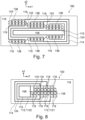
- the embodiment illustrated in the schematic plan view of FIG. 7 is similar to the embodiment of FIG. 6 with respect to the geometric arrangement of the protection devices 119.
- the semiconductor device 100 of FIG. 7 includes not only a serial connection of protection elements 119, but also a parallel connection of two protection structures. In some other embodiments, more than two protection structures may be electrically connected in parallel, for example.
- the semiconductor device 100 illustrated in the FIG. 7 includes cascaded level shifter elements 142.
- One level shifter element 142 and one protection element 119 are surrounded by a common third trench isolation structure 138.
- the protection element 119 may limit the voltage over the level shifter element 142.
- the level shifter elements may also be electrically separated from the protection elements by a trench isolation structure, for example.
- a level shifter element may also be connected in parallel with a voltage limiting element, e.g. a Zener diode.
- FIG. 8 illustrates an embodiment of the semiconductor devices 100 having a plurality of protection elements 119 arranged in a meandering configuration and serially connected to one another along the meandering configuration.
- the protection elements 119 and level shifter elements 142 may be arranged in a variety of ways. A specific arrangement may be chosen depending on the breakdown voltage or blocking voltage capability of the trench isolation structures and the maximum voltage ratings of the protection elements 119 and level shifter elements 142, for example.
- a stack or chain of protection elements 190 or level shifter elements 142 may be laterally surrounded by trench isolation structures or other isolation structures and may be arranged in or around the area to be protected.
- the chain of stacked elements may be arranged in a way that a maximum isolation capability of a single separation/trench isolation structure is ensured in case that the voltage protection capability of a single protection element is lower than the isolation capability of the single separation/trench isolation structure.
- a geometric arrangement of the stacked protection elements may include handling of voltage differences in two orientations, for example. Along a first orientation, e.g. the second lateral direction x2 in the embodiment illustrated in FIG. 5 , voltage differences between different areas, e.g.
- the first protection sub-area 1121 and the second protection sub-area 1122 are absorbed.
- the protection elements 119 are stacked to achieve protection for voltage differences that depend on the maximum voltage ratings of the manufacturing process technology.
- the wiring 140 may be placed over a separation/trench isolation structure to achieve a chain structure for the stacked protection elements. Thus, unprotected areas may be avoided and cascaded level shifter elements may be supported for data exchange between different active areas.
- a semiconductor device 200 includes a substrate 202.
- An isolation structure 204 is formed on the substrate 202.
- a first active area 208 and a second active area 216 are formed on the isolation structure 204.
- a trench isolation structure 210 electrically separates the first active area 208 and the second active area 216.
- At least two device elements 218, e.g. level shifter elements or protection elements are formed in the second active area 216 and are connected in series.
- the at least two device elements 218 are arranged along a sidewall 250 of the trench isolation structure 210 parallel to an extension direction of the sidewall 250.
- a longitudinal direction of some or all of the device elements 218 may be arranged at a tilt angle with respect to an extension direction of the sidewall 250, for example.
- the device elements 218 may also adjoin one another.
- all or some of the device elements may also directly adjoin the sidewall 250.
- the substrate 202 may be removed, e.g. by grinding, etching or any other suitable process, during the production process to achieve a very thin semiconductor device with the isolation structure 204 as a lowermost layer for achieving a better thermal behavior of the semiconductor device.
- Circuit elements may be formed in each of the first and second active areas 208, 216, for example.
Landscapes
- Semiconductor Integrated Circuits (AREA)
- Element Separation (AREA)
Claims (9)
- Halbleiterelement (100), umfassend:eine Isolationsstruktur (104);eine erste aktive Fläche (108), die auf der Isolationsstruktur (104) ausgebildet ist;eine Schutzfläche (112), die auf der Isolationsstruktur (104) ausgebildet ist und die erste aktive Fläche (108) seitlich umgibt;eine zweite aktive Fläche (116), die auf der Isolationsstruktur (104) ausgebildet ist und die Schutzfläche (112) seitlich umgibt;eine erste Grabenisolationsstruktur (110), die die erste aktive Fläche (108) und die Schutzfläche (112) elektrisch trennt;eine zweite Grabenisolationsstruktur (114), die die Schutzfläche (112) und die zweite aktive Fläche (116) elektrisch trennt; undeine Schutzstruktur (118) in der Schutzfläche (112), wobei ein erster Kontakt (120) der Schutzstruktur (118) elektrisch mit der ersten aktiven Fläche (108) verbunden ist und ein zweiter Kontakt (122) der Schutzstruktur (118) elektrisch mit der zweiten aktiven Fläche (116) verbunden ist,dadurch gekennzeichnet, dassdie Schutzstruktur (118) eine Mehrzahl von Schutzelementen (119) umfasst, die fortlaufend im Wesentlichen entlang einer Seitenwand der ersten Grabenisolationsstruktur (110) angeordnet und seriell miteinander im Wesentlichen entlang der Seitenwand der ersten Grabenisolationsstruktur (110) verbunden sind, und jedes oder Gruppen der Mehrzahl von Schutzelementen (119) seitlich von einer geschlossenen Graben-Vorrichtungsisolationsstruktur umgeben sind, die die erste aktive Fläche (108) nicht umgibt.
- Halbleiterelement (100) nach Anspruch 1, wobei die Vorrichtungsisolationsstruktur eine dritte Grabenisolationsstruktur (138) umfasst, und eine Breite der dritten Grabenisolationsstruktur (138) einer Breite jeder der ersten und zweiten Grabenisolationsstrukturen (110, 114) entspricht.
- Halbleiterelement (100) nach einem der vorhergehenden Ansprüche, wobeidie Schutzfläche (112) mindestens ein Paar Schutzteilflächen umfasst,eine erste Schutzteilfläche (1121) jedes Paars des mindestens einen Paars seitlich eine zweite Schutzteilfläche (1122) des jeweiligen Paars umgibt; und das Halbleiterelement (100) ferner umfasst eine vierte Grabenisolationsstruktur (124), die zwischen der ersten Schutzteilfläche (1121) und der zweiten Schutzteilfläche (1122) angeordnet ist.
- Halbleiterelement (100) nach Anspruch 3, wobei die Schutzstruktur (118) eine erste Anzahl von seriell verbundenen Schutzelementen (119) in der ersten Schutzteilfläche (1121) und eine zweite Anzahl von seriell verbundenen Schutzelementen (119) in der zweiten Schutzteilfläche (1122) umfasst.
- Halbleiterelement (100) nach Anspruch 4, wobei die erste Anzahl von Schutzelementen (119) fortlaufend entlang der ersten lateralen Richtung (x1) angeordnet ist, und die zweite Anzahl von Schutzelementen (119) fortlaufend entlang der ersten lateralen Richtung (x1) mit einem lateralen Versatz zu der ersten Anzahl von Schutzelementen (119) angeordnet ist, und wobei der laterale Versatz ein Versatz entlang einer zweiten lateralen Richtung (x2) rechtwinklig zu der ersten lateralen Richtung (x1) ist.
- Halbleiterelement nach einem der vorhergehenden Ansprüche, ferner umfassend:
eine Pegelwandlerstruktur in der Schutzfläche (112). - Halbleiterelement nach einem der vorhergehenden Ansprüche, ferner umfassend:eine High-Side-Gate-Treiberschaltung in der ersten aktiven Fläche (108); undeine Low-Side-Gate-Treiberschaltung in der zweiten aktiven Fläche (116).
- Halbleiterelement nach Anspruch 1, wobei ein Teil der geschlossenen Graben-Elementisolationsstruktur von mindestens einem der Mehrzahl von Schutzelementen (119) einem Teil der ersten Grabenisolationsstruktur (110) entspricht.
- Verfahren zum Herstellen eines Halbleiterelements (100), wobei das Verfahren umfasst:Bereitstellen eines Halbleiterkörpers, umfassend eine Isolationsstruktur (104), eine erste aktive Fläche (108), die auf der Isolationsstruktur (104) ausgebildet ist, eine Schutzfläche (112), die auf der Isolationsstruktur (104) ausgebildet ist und die erste aktive Fläche (108) seitlich umgibt, und eine zweite aktive Fläche (116), die auf der Isolationsstruktur (104) ausgebildet ist und die Schutzfläche (112) seitlich umgibt;Ausbilden einer ersten Grabenisolationsstruktur (110), wobei die erste Grabenisolationsstruktur (110) die erste aktive Fläche (108) und die Schutzfläche (112) elektrisch trennt;Ausbilden einer zweiten Grabenisolationsstruktur (114), wobei die zweite Grabenisolationsstruktur (110) die Schutzfläche (112) und die zweite aktive Fläche (116) elektrisch trennt;Ausbilden einer Schutzstruktur (118) in der Schutzfläche (112), wobei die Schutzstruktur (118) eine Mehrzahl von Schutzelementen (119) umfasst, die fortlaufend im Wesentlichen entlang einer Seitenwand der ersten Grabenisolationsstruktur (110) angeordnet und seriell miteinander im Wesentlichen entlang der Seitenwand der ersten Grabenisolationsstruktur (110) verbunden sind;elektrisches Verbinden eines ersten Kontakts (120) der Schutzstruktur (118) mit der ersten aktiven Fläche (108); undelektrisches Verbinden eines zweiten Kontakts (122) der Schutzstruktur (118) mit der zweiten aktiven Fläche (116), wobei das Verfahren ferner das Ausbilden einer geschlossenen Graben-Elementisolationsstruktur umfasst, die seitlich jedes oder Gruppen der Mehrzahl von Schutzelementen (119) umgibt und die erste aktive Fläche (108) nicht umgibt.
Priority Applications (2)
| Application Number | Priority Date | Filing Date | Title |
|---|---|---|---|
| EP19156506.8A EP3693993B1 (de) | 2019-02-11 | 2019-02-11 | Halbleiterbauelement mit schutzstruktur und herstellungsverfahren dafür |
| US16/784,483 US20200258775A1 (en) | 2019-02-11 | 2020-02-07 | Semiconductor Device Including Protection Structure and Manufacturing Method Therefor |
Applications Claiming Priority (1)
| Application Number | Priority Date | Filing Date | Title |
|---|---|---|---|
| EP19156506.8A EP3693993B1 (de) | 2019-02-11 | 2019-02-11 | Halbleiterbauelement mit schutzstruktur und herstellungsverfahren dafür |
Publications (3)
| Publication Number | Publication Date |
|---|---|
| EP3693993A1 EP3693993A1 (de) | 2020-08-12 |
| EP3693993A8 EP3693993A8 (de) | 2020-09-02 |
| EP3693993B1 true EP3693993B1 (de) | 2025-07-09 |
Family
ID=65408995
Family Applications (1)
| Application Number | Title | Priority Date | Filing Date |
|---|---|---|---|
| EP19156506.8A Active EP3693993B1 (de) | 2019-02-11 | 2019-02-11 | Halbleiterbauelement mit schutzstruktur und herstellungsverfahren dafür |
Country Status (2)
| Country | Link |
|---|---|
| US (1) | US20200258775A1 (de) |
| EP (1) | EP3693993B1 (de) |
Families Citing this family (2)
| Publication number | Priority date | Publication date | Assignee | Title |
|---|---|---|---|---|
| US11817403B2 (en) | 2021-03-11 | 2023-11-14 | Taiwan Semiconductor Manufacturing Co., Ltd. | Electrostatic discharge (ESD) array with circuit controlled switches |
| CN120417488A (zh) * | 2024-01-30 | 2025-08-01 | 达尔科技股份有限公司 | 静电放电保护结构、半导体功率器件与半导体功率器件的制造方法 |
Family Cites Families (4)
| Publication number | Priority date | Publication date | Assignee | Title |
|---|---|---|---|---|
| FR2803099B1 (fr) * | 1999-12-22 | 2002-08-16 | St Microelectronics Sa | Dispositif de protection d'une structure soi |
| EP1302984A1 (de) * | 2001-10-09 | 2003-04-16 | STMicroelectronics S.r.l. | Schutzstruktur gegen elektrostatische Entladungen (ESD) für ein auf einem SOI-Substrat integriertes elektronisches Bauelement und entsprechendes Integrationsverfahren |
| JP4935164B2 (ja) * | 2006-04-14 | 2012-05-23 | 株式会社デンソー | 半導体装置 |
| JP4993092B2 (ja) * | 2007-05-31 | 2012-08-08 | 富士電機株式会社 | レベルシフト回路および半導体装置 |
-
2019
- 2019-02-11 EP EP19156506.8A patent/EP3693993B1/de active Active
-
2020
- 2020-02-07 US US16/784,483 patent/US20200258775A1/en not_active Abandoned
Also Published As
| Publication number | Publication date |
|---|---|
| EP3693993A1 (de) | 2020-08-12 |
| EP3693993A8 (de) | 2020-09-02 |
| US20200258775A1 (en) | 2020-08-13 |
Similar Documents
| Publication | Publication Date | Title |
|---|---|---|
| US11456596B2 (en) | USB type-C load switch ESD protection | |
| US8222698B2 (en) | Bond pad with integrated transient over-voltage protection | |
| US8749018B2 (en) | Integrated semiconductor device having an insulating structure and a manufacturing method | |
| US12159815B2 (en) | Connection arrangements for integrated lateral diffusion field effect transistors having a backside contact | |
| EP0011443B1 (de) | Integrierte Halbleiterschaltung | |
| US12183730B2 (en) | Silicon controlled rectifier | |
| EP4187603B1 (de) | Esd-schutzvorrichtung mit isolationsstrukturanordnung zur minimierung der harmonischen verzerrung | |
| EP3693993B1 (de) | Halbleiterbauelement mit schutzstruktur und herstellungsverfahren dafür | |
| US12394759B2 (en) | Semiconductor device and circuit device | |
| US20080006847A1 (en) | Semiconductor protective structure for electrostatic discharge | |
| US11121126B2 (en) | Silicon controlled rectifier and manufacturing method therefor | |
| US6392276B1 (en) | Device for protecting an SOI structure | |
| KR102463902B1 (ko) | 다이오드를 내장한 mos 구조의 사이리스터 소자 | |
| CN112185955A (zh) | 垂直式双极性晶体管装置 | |
| US20230215862A1 (en) | Semiconductor device and bidirectional esd protection device comprising the same | |
| US20260068304A1 (en) | Latch-up prevention and increased decoupling capacitor density | |
| CN112185954B (zh) | 垂直式双极性晶体管装置 | |
| CN117616572A (zh) | 半导体装置及其制造方法 | |
| CN121078804A (zh) | 一种半导体器件及其制造方法 | |
| KR20230036859A (ko) | 정전기 방전 보호 소자 및 이를 포함하는 반도체 장치 |
Legal Events
| Date | Code | Title | Description |
|---|---|---|---|
| PUAI | Public reference made under article 153(3) epc to a published international application that has entered the european phase |
Free format text: ORIGINAL CODE: 0009012 |
|
| STAA | Information on the status of an ep patent application or granted ep patent |
Free format text: STATUS: THE APPLICATION HAS BEEN PUBLISHED |
|
| AK | Designated contracting states |
Kind code of ref document: A1 Designated state(s): AL AT BE BG CH CY CZ DE DK EE ES FI FR GB GR HR HU IE IS IT LI LT LU LV MC MK MT NL NO PL PT RO RS SE SI SK SM TR |
|
| AX | Request for extension of the european patent |
Extension state: BA ME |
|
| STAA | Information on the status of an ep patent application or granted ep patent |
Free format text: STATUS: REQUEST FOR EXAMINATION WAS MADE |
|
| 17P | Request for examination filed |
Effective date: 20210211 |
|
| RBV | Designated contracting states (corrected) |
Designated state(s): AL AT BE BG CH CY CZ DE DK EE ES FI FR GB GR HR HU IE IS IT LI LT LU LV MC MK MT NL NO PL PT RO RS SE SI SK SM TR |
|
| STAA | Information on the status of an ep patent application or granted ep patent |
Free format text: STATUS: EXAMINATION IS IN PROGRESS |
|
| 17Q | First examination report despatched |
Effective date: 20230329 |
|
| REG | Reference to a national code |
Ref country code: DE Ref legal event code: R079 Free format text: PREVIOUS MAIN CLASS: H01L0027020000 Ipc: H10D0086000000 Ref document number: 602019072206 Country of ref document: DE |
|
| GRAP | Despatch of communication of intention to grant a patent |
Free format text: ORIGINAL CODE: EPIDOSNIGR1 |
|
| STAA | Information on the status of an ep patent application or granted ep patent |
Free format text: STATUS: GRANT OF PATENT IS INTENDED |
|
| RIC1 | Information provided on ipc code assigned before grant |
Ipc: H01L 21/762 20060101ALI20250116BHEP Ipc: H10D 89/60 20250101ALI20250116BHEP Ipc: H10D 86/00 20250101AFI20250116BHEP |
|
| INTG | Intention to grant announced |
Effective date: 20250207 |
|
| P01 | Opt-out of the competence of the unified patent court (upc) registered |
Free format text: CASE NUMBER: APP_10081/2025 Effective date: 20250227 |
|
| GRAS | Grant fee paid |
Free format text: ORIGINAL CODE: EPIDOSNIGR3 |
|
| GRAA | (expected) grant |
Free format text: ORIGINAL CODE: 0009210 |
|
| STAA | Information on the status of an ep patent application or granted ep patent |
Free format text: STATUS: THE PATENT HAS BEEN GRANTED |
|
| AK | Designated contracting states |
Kind code of ref document: B1 Designated state(s): AL AT BE BG CH CY CZ DE DK EE ES FI FR GB GR HR HU IE IS IT LI LT LU LV MC MK MT NL NO PL PT RO RS SE SI SK SM TR |
|
| REG | Reference to a national code |
Ref country code: GB Ref legal event code: FG4D |
|
| REG | Reference to a national code |
Ref country code: CH Ref legal event code: EP |
|
| REG | Reference to a national code |
Ref country code: IE Ref legal event code: FG4D |
|
| REG | Reference to a national code |
Ref country code: DE Ref legal event code: R096 Ref document number: 602019072206 Country of ref document: DE |
|
| REG | Reference to a national code |
Ref country code: NL Ref legal event code: MP Effective date: 20250709 |
|
| PG25 | Lapsed in a contracting state [announced via postgrant information from national office to epo] |
Ref country code: PT Free format text: LAPSE BECAUSE OF FAILURE TO SUBMIT A TRANSLATION OF THE DESCRIPTION OR TO PAY THE FEE WITHIN THE PRESCRIBED TIME-LIMIT Effective date: 20251110 |
|
| PG25 | Lapsed in a contracting state [announced via postgrant information from national office to epo] |
Ref country code: NL Free format text: LAPSE BECAUSE OF FAILURE TO SUBMIT A TRANSLATION OF THE DESCRIPTION OR TO PAY THE FEE WITHIN THE PRESCRIBED TIME-LIMIT Effective date: 20250709 |
|
| REG | Reference to a national code |
Ref country code: AT Ref legal event code: MK05 Ref document number: 1813118 Country of ref document: AT Kind code of ref document: T Effective date: 20250709 |
|
| PG25 | Lapsed in a contracting state [announced via postgrant information from national office to epo] |
Ref country code: IS Free format text: LAPSE BECAUSE OF FAILURE TO SUBMIT A TRANSLATION OF THE DESCRIPTION OR TO PAY THE FEE WITHIN THE PRESCRIBED TIME-LIMIT Effective date: 20251109 |
|
| PG25 | Lapsed in a contracting state [announced via postgrant information from national office to epo] |
Ref country code: NO Free format text: LAPSE BECAUSE OF FAILURE TO SUBMIT A TRANSLATION OF THE DESCRIPTION OR TO PAY THE FEE WITHIN THE PRESCRIBED TIME-LIMIT Effective date: 20251009 |
|
| REG | Reference to a national code |
Ref country code: LT Ref legal event code: MG9D |
|
| PG25 | Lapsed in a contracting state [announced via postgrant information from national office to epo] |
Ref country code: AT Free format text: LAPSE BECAUSE OF FAILURE TO SUBMIT A TRANSLATION OF THE DESCRIPTION OR TO PAY THE FEE WITHIN THE PRESCRIBED TIME-LIMIT Effective date: 20250709 |
|
| PG25 | Lapsed in a contracting state [announced via postgrant information from national office to epo] |
Ref country code: FI Free format text: LAPSE BECAUSE OF FAILURE TO SUBMIT A TRANSLATION OF THE DESCRIPTION OR TO PAY THE FEE WITHIN THE PRESCRIBED TIME-LIMIT Effective date: 20250709 |
|
| PG25 | Lapsed in a contracting state [announced via postgrant information from national office to epo] |
Ref country code: HR Free format text: LAPSE BECAUSE OF FAILURE TO SUBMIT A TRANSLATION OF THE DESCRIPTION OR TO PAY THE FEE WITHIN THE PRESCRIBED TIME-LIMIT Effective date: 20250709 |
|
| PG25 | Lapsed in a contracting state [announced via postgrant information from national office to epo] |
Ref country code: GR Free format text: LAPSE BECAUSE OF FAILURE TO SUBMIT A TRANSLATION OF THE DESCRIPTION OR TO PAY THE FEE WITHIN THE PRESCRIBED TIME-LIMIT Effective date: 20251010 |
|
| PG25 | Lapsed in a contracting state [announced via postgrant information from national office to epo] |
Ref country code: SE Free format text: LAPSE BECAUSE OF FAILURE TO SUBMIT A TRANSLATION OF THE DESCRIPTION OR TO PAY THE FEE WITHIN THE PRESCRIBED TIME-LIMIT Effective date: 20250709 |
|
| PG25 | Lapsed in a contracting state [announced via postgrant information from national office to epo] |
Ref country code: LV Free format text: LAPSE BECAUSE OF FAILURE TO SUBMIT A TRANSLATION OF THE DESCRIPTION OR TO PAY THE FEE WITHIN THE PRESCRIBED TIME-LIMIT Effective date: 20250709 |
|
| PG25 | Lapsed in a contracting state [announced via postgrant information from national office to epo] |
Ref country code: BG Free format text: LAPSE BECAUSE OF FAILURE TO SUBMIT A TRANSLATION OF THE DESCRIPTION OR TO PAY THE FEE WITHIN THE PRESCRIBED TIME-LIMIT Effective date: 20250709 Ref country code: PL Free format text: LAPSE BECAUSE OF FAILURE TO SUBMIT A TRANSLATION OF THE DESCRIPTION OR TO PAY THE FEE WITHIN THE PRESCRIBED TIME-LIMIT Effective date: 20250709 |
|
| PG25 | Lapsed in a contracting state [announced via postgrant information from national office to epo] |
Ref country code: RS Free format text: LAPSE BECAUSE OF FAILURE TO SUBMIT A TRANSLATION OF THE DESCRIPTION OR TO PAY THE FEE WITHIN THE PRESCRIBED TIME-LIMIT Effective date: 20251009 |
|
| PG25 | Lapsed in a contracting state [announced via postgrant information from national office to epo] |
Ref country code: ES Free format text: LAPSE BECAUSE OF FAILURE TO SUBMIT A TRANSLATION OF THE DESCRIPTION OR TO PAY THE FEE WITHIN THE PRESCRIBED TIME-LIMIT Effective date: 20250709 |
|
| PG25 | Lapsed in a contracting state [announced via postgrant information from national office to epo] |
Ref country code: SM Free format text: LAPSE BECAUSE OF FAILURE TO SUBMIT A TRANSLATION OF THE DESCRIPTION OR TO PAY THE FEE WITHIN THE PRESCRIBED TIME-LIMIT Effective date: 20250709 |
|
| PG25 | Lapsed in a contracting state [announced via postgrant information from national office to epo] |
Ref country code: DK Free format text: LAPSE BECAUSE OF FAILURE TO SUBMIT A TRANSLATION OF THE DESCRIPTION OR TO PAY THE FEE WITHIN THE PRESCRIBED TIME-LIMIT Effective date: 20250709 |
|
| PG25 | Lapsed in a contracting state [announced via postgrant information from national office to epo] |
Ref country code: IT Free format text: LAPSE BECAUSE OF FAILURE TO SUBMIT A TRANSLATION OF THE DESCRIPTION OR TO PAY THE FEE WITHIN THE PRESCRIBED TIME-LIMIT Effective date: 20250709 |