EP3690952A1 - Dispositif semiconducteur à grille à tranchée et son procédé de fabrication - Google Patents
Dispositif semiconducteur à grille à tranchée et son procédé de fabrication Download PDFInfo
- Publication number
- EP3690952A1 EP3690952A1 EP19154245.5A EP19154245A EP3690952A1 EP 3690952 A1 EP3690952 A1 EP 3690952A1 EP 19154245 A EP19154245 A EP 19154245A EP 3690952 A1 EP3690952 A1 EP 3690952A1
- Authority
- EP
- European Patent Office
- Prior art keywords
- trench
- region
- source
- gate
- semiconductor layer
- Prior art date
- Legal status (The legal status is an assumption and is not a legal conclusion. Google has not performed a legal analysis and makes no representation as to the accuracy of the status listed.)
- Pending
Links
- 239000004065 semiconductor Substances 0.000 title claims abstract description 107
- 238000004519 manufacturing process Methods 0.000 title claims abstract description 8
- 238000000034 method Methods 0.000 title claims description 24
- 210000000746 body region Anatomy 0.000 claims description 46
- 239000000758 substrate Substances 0.000 claims description 13
- 239000007943 implant Substances 0.000 description 26
- 230000015572 biosynthetic process Effects 0.000 description 15
- 238000001465 metallisation Methods 0.000 description 11
- XUIMIQQOPSSXEZ-UHFFFAOYSA-N Silicon Chemical compound [Si] XUIMIQQOPSSXEZ-UHFFFAOYSA-N 0.000 description 8
- 238000005530 etching Methods 0.000 description 8
- 229910052710 silicon Inorganic materials 0.000 description 8
- 239000010703 silicon Substances 0.000 description 8
- 230000001419 dependent effect Effects 0.000 description 5
- BOTDANWDWHJENH-UHFFFAOYSA-N Tetraethyl orthosilicate Chemical compound CCO[Si](OCC)(OCC)OCC BOTDANWDWHJENH-UHFFFAOYSA-N 0.000 description 3
- 238000000151 deposition Methods 0.000 description 3
- ZOXJGFHDIHLPTG-UHFFFAOYSA-N Boron Chemical compound [B] ZOXJGFHDIHLPTG-UHFFFAOYSA-N 0.000 description 2
- 229910052796 boron Inorganic materials 0.000 description 2
- 239000000969 carrier Substances 0.000 description 2
- 230000015556 catabolic process Effects 0.000 description 2
- 230000008021 deposition Effects 0.000 description 2
- 238000002513 implantation Methods 0.000 description 2
- 229910052751 metal Inorganic materials 0.000 description 2
- 239000002184 metal Substances 0.000 description 2
- 229910021420 polycrystalline silicon Inorganic materials 0.000 description 2
- PXGOKWXKJXAPGV-UHFFFAOYSA-N Fluorine Chemical compound FF PXGOKWXKJXAPGV-UHFFFAOYSA-N 0.000 description 1
- 239000004411 aluminium Substances 0.000 description 1
- 229910052782 aluminium Inorganic materials 0.000 description 1
- XAGFODPZIPBFFR-UHFFFAOYSA-N aluminium Chemical compound [Al] XAGFODPZIPBFFR-UHFFFAOYSA-N 0.000 description 1
- 229910052785 arsenic Inorganic materials 0.000 description 1
- RQNWIZPPADIBDY-UHFFFAOYSA-N arsenic atom Chemical compound [As] RQNWIZPPADIBDY-UHFFFAOYSA-N 0.000 description 1
- 230000000694 effects Effects 0.000 description 1
- 230000005684 electric field Effects 0.000 description 1
- 229910052731 fluorine Inorganic materials 0.000 description 1
- 239000011737 fluorine Substances 0.000 description 1
- 239000011810 insulating material Substances 0.000 description 1
- 230000003647 oxidation Effects 0.000 description 1
- 238000007254 oxidation reaction Methods 0.000 description 1
- 230000000149 penetrating effect Effects 0.000 description 1
- 238000000206 photolithography Methods 0.000 description 1
- 238000005498 polishing Methods 0.000 description 1
- 229920005591 polysilicon Polymers 0.000 description 1
- 229910021332 silicide Inorganic materials 0.000 description 1
- FVBUAEGBCNSCDD-UHFFFAOYSA-N silicide(4-) Chemical compound [Si-4] FVBUAEGBCNSCDD-UHFFFAOYSA-N 0.000 description 1
- 239000000126 substance Substances 0.000 description 1
- WQJQOUPTWCFRMM-UHFFFAOYSA-N tungsten disilicide Chemical compound [Si]#[W]#[Si] WQJQOUPTWCFRMM-UHFFFAOYSA-N 0.000 description 1
- 229910021342 tungsten silicide Inorganic materials 0.000 description 1
Images


Classifications
-
- H—ELECTRICITY
- H01—ELECTRIC ELEMENTS
- H01L—SEMICONDUCTOR DEVICES NOT COVERED BY CLASS H10
- H01L29/00—Semiconductor devices adapted for rectifying, amplifying, oscillating or switching, or capacitors or resistors with at least one potential-jump barrier or surface barrier, e.g. PN junction depletion layer or carrier concentration layer; Details of semiconductor bodies or of electrodes thereof ; Multistep manufacturing processes therefor
- H01L29/66—Types of semiconductor device ; Multistep manufacturing processes therefor
- H01L29/68—Types of semiconductor device ; Multistep manufacturing processes therefor controllable by only the electric current supplied, or only the electric potential applied, to an electrode which does not carry the current to be rectified, amplified or switched
- H01L29/76—Unipolar devices, e.g. field effect transistors
- H01L29/772—Field effect transistors
- H01L29/78—Field effect transistors with field effect produced by an insulated gate
- H01L29/7827—Vertical transistors
-
- H—ELECTRICITY
- H01—ELECTRIC ELEMENTS
- H01L—SEMICONDUCTOR DEVICES NOT COVERED BY CLASS H10
- H01L29/00—Semiconductor devices adapted for rectifying, amplifying, oscillating or switching, or capacitors or resistors with at least one potential-jump barrier or surface barrier, e.g. PN junction depletion layer or carrier concentration layer; Details of semiconductor bodies or of electrodes thereof ; Multistep manufacturing processes therefor
- H01L29/02—Semiconductor bodies ; Multistep manufacturing processes therefor
- H01L29/06—Semiconductor bodies ; Multistep manufacturing processes therefor characterised by their shape; characterised by the shapes, relative sizes, or dispositions of the semiconductor regions ; characterised by the concentration or distribution of impurities within semiconductor regions
- H01L29/08—Semiconductor bodies ; Multistep manufacturing processes therefor characterised by their shape; characterised by the shapes, relative sizes, or dispositions of the semiconductor regions ; characterised by the concentration or distribution of impurities within semiconductor regions with semiconductor regions connected to an electrode carrying current to be rectified, amplified or switched and such electrode being part of a semiconductor device which comprises three or more electrodes
- H01L29/0843—Source or drain regions of field-effect devices
- H01L29/0847—Source or drain regions of field-effect devices of field-effect transistors with insulated gate
- H01L29/0852—Source or drain regions of field-effect devices of field-effect transistors with insulated gate of DMOS transistors
- H01L29/0856—Source regions
- H01L29/0869—Shape
-
- H—ELECTRICITY
- H01—ELECTRIC ELEMENTS
- H01L—SEMICONDUCTOR DEVICES NOT COVERED BY CLASS H10
- H01L29/00—Semiconductor devices adapted for rectifying, amplifying, oscillating or switching, or capacitors or resistors with at least one potential-jump barrier or surface barrier, e.g. PN junction depletion layer or carrier concentration layer; Details of semiconductor bodies or of electrodes thereof ; Multistep manufacturing processes therefor
- H01L29/02—Semiconductor bodies ; Multistep manufacturing processes therefor
- H01L29/06—Semiconductor bodies ; Multistep manufacturing processes therefor characterised by their shape; characterised by the shapes, relative sizes, or dispositions of the semiconductor regions ; characterised by the concentration or distribution of impurities within semiconductor regions
- H01L29/0684—Semiconductor bodies ; Multistep manufacturing processes therefor characterised by their shape; characterised by the shapes, relative sizes, or dispositions of the semiconductor regions ; characterised by the concentration or distribution of impurities within semiconductor regions characterised by the shape, relative sizes or dispositions of the semiconductor regions or junctions between the regions
-
- H—ELECTRICITY
- H01—ELECTRIC ELEMENTS
- H01L—SEMICONDUCTOR DEVICES NOT COVERED BY CLASS H10
- H01L29/00—Semiconductor devices adapted for rectifying, amplifying, oscillating or switching, or capacitors or resistors with at least one potential-jump barrier or surface barrier, e.g. PN junction depletion layer or carrier concentration layer; Details of semiconductor bodies or of electrodes thereof ; Multistep manufacturing processes therefor
- H01L29/02—Semiconductor bodies ; Multistep manufacturing processes therefor
- H01L29/06—Semiconductor bodies ; Multistep manufacturing processes therefor characterised by their shape; characterised by the shapes, relative sizes, or dispositions of the semiconductor regions ; characterised by the concentration or distribution of impurities within semiconductor regions
- H01L29/08—Semiconductor bodies ; Multistep manufacturing processes therefor characterised by their shape; characterised by the shapes, relative sizes, or dispositions of the semiconductor regions ; characterised by the concentration or distribution of impurities within semiconductor regions with semiconductor regions connected to an electrode carrying current to be rectified, amplified or switched and such electrode being part of a semiconductor device which comprises three or more electrodes
- H01L29/0843—Source or drain regions of field-effect devices
- H01L29/0847—Source or drain regions of field-effect devices of field-effect transistors with insulated gate
-
- H—ELECTRICITY
- H01—ELECTRIC ELEMENTS
- H01L—SEMICONDUCTOR DEVICES NOT COVERED BY CLASS H10
- H01L29/00—Semiconductor devices adapted for rectifying, amplifying, oscillating or switching, or capacitors or resistors with at least one potential-jump barrier or surface barrier, e.g. PN junction depletion layer or carrier concentration layer; Details of semiconductor bodies or of electrodes thereof ; Multistep manufacturing processes therefor
- H01L29/40—Electrodes ; Multistep manufacturing processes therefor
- H01L29/41—Electrodes ; Multistep manufacturing processes therefor characterised by their shape, relative sizes or dispositions
- H01L29/417—Electrodes ; Multistep manufacturing processes therefor characterised by their shape, relative sizes or dispositions carrying the current to be rectified, amplified or switched
- H01L29/41725—Source or drain electrodes for field effect devices
- H01L29/41741—Source or drain electrodes for field effect devices for vertical or pseudo-vertical devices
-
- H—ELECTRICITY
- H01—ELECTRIC ELEMENTS
- H01L—SEMICONDUCTOR DEVICES NOT COVERED BY CLASS H10
- H01L29/00—Semiconductor devices adapted for rectifying, amplifying, oscillating or switching, or capacitors or resistors with at least one potential-jump barrier or surface barrier, e.g. PN junction depletion layer or carrier concentration layer; Details of semiconductor bodies or of electrodes thereof ; Multistep manufacturing processes therefor
- H01L29/40—Electrodes ; Multistep manufacturing processes therefor
- H01L29/41—Electrodes ; Multistep manufacturing processes therefor characterised by their shape, relative sizes or dispositions
- H01L29/417—Electrodes ; Multistep manufacturing processes therefor characterised by their shape, relative sizes or dispositions carrying the current to be rectified, amplified or switched
- H01L29/41725—Source or drain electrodes for field effect devices
- H01L29/41766—Source or drain electrodes for field effect devices with at least part of the source or drain electrode having contact below the semiconductor surface, e.g. the source or drain electrode formed at least partially in a groove or with inclusions of conductor inside the semiconductor
-
- H—ELECTRICITY
- H01—ELECTRIC ELEMENTS
- H01L—SEMICONDUCTOR DEVICES NOT COVERED BY CLASS H10
- H01L29/00—Semiconductor devices adapted for rectifying, amplifying, oscillating or switching, or capacitors or resistors with at least one potential-jump barrier or surface barrier, e.g. PN junction depletion layer or carrier concentration layer; Details of semiconductor bodies or of electrodes thereof ; Multistep manufacturing processes therefor
- H01L29/40—Electrodes ; Multistep manufacturing processes therefor
- H01L29/41—Electrodes ; Multistep manufacturing processes therefor characterised by their shape, relative sizes or dispositions
- H01L29/417—Electrodes ; Multistep manufacturing processes therefor characterised by their shape, relative sizes or dispositions carrying the current to be rectified, amplified or switched
- H01L29/41725—Source or drain electrodes for field effect devices
- H01L29/41775—Source or drain electrodes for field effect devices characterised by the proximity or the relative position of the source or drain electrode and the gate electrode, e.g. the source or drain electrode separated from the gate electrode by side-walls or spreading around or above the gate electrode
-
- H—ELECTRICITY
- H01—ELECTRIC ELEMENTS
- H01L—SEMICONDUCTOR DEVICES NOT COVERED BY CLASS H10
- H01L29/00—Semiconductor devices adapted for rectifying, amplifying, oscillating or switching, or capacitors or resistors with at least one potential-jump barrier or surface barrier, e.g. PN junction depletion layer or carrier concentration layer; Details of semiconductor bodies or of electrodes thereof ; Multistep manufacturing processes therefor
- H01L29/40—Electrodes ; Multistep manufacturing processes therefor
- H01L29/41—Electrodes ; Multistep manufacturing processes therefor characterised by their shape, relative sizes or dispositions
- H01L29/423—Electrodes ; Multistep manufacturing processes therefor characterised by their shape, relative sizes or dispositions not carrying the current to be rectified, amplified or switched
- H01L29/42312—Gate electrodes for field effect devices
- H01L29/42316—Gate electrodes for field effect devices for field-effect transistors
- H01L29/4232—Gate electrodes for field effect devices for field-effect transistors with insulated gate
- H01L29/42356—Disposition, e.g. buried gate electrode
- H01L29/4236—Disposition, e.g. buried gate electrode within a trench, e.g. trench gate electrode, groove gate electrode
-
- H—ELECTRICITY
- H01—ELECTRIC ELEMENTS
- H01L—SEMICONDUCTOR DEVICES NOT COVERED BY CLASS H10
- H01L29/00—Semiconductor devices adapted for rectifying, amplifying, oscillating or switching, or capacitors or resistors with at least one potential-jump barrier or surface barrier, e.g. PN junction depletion layer or carrier concentration layer; Details of semiconductor bodies or of electrodes thereof ; Multistep manufacturing processes therefor
- H01L29/66—Types of semiconductor device ; Multistep manufacturing processes therefor
- H01L29/66007—Multistep manufacturing processes
- H01L29/66075—Multistep manufacturing processes of devices having semiconductor bodies comprising group 14 or group 13/15 materials
- H01L29/66227—Multistep manufacturing processes of devices having semiconductor bodies comprising group 14 or group 13/15 materials the devices being controllable only by the electric current supplied or the electric potential applied, to an electrode which does not carry the current to be rectified, amplified or switched, e.g. three-terminal devices
- H01L29/66409—Unipolar field-effect transistors
- H01L29/66477—Unipolar field-effect transistors with an insulated gate, i.e. MISFET
- H01L29/66666—Vertical transistors
-
- H—ELECTRICITY
- H01—ELECTRIC ELEMENTS
- H01L—SEMICONDUCTOR DEVICES NOT COVERED BY CLASS H10
- H01L29/00—Semiconductor devices adapted for rectifying, amplifying, oscillating or switching, or capacitors or resistors with at least one potential-jump barrier or surface barrier, e.g. PN junction depletion layer or carrier concentration layer; Details of semiconductor bodies or of electrodes thereof ; Multistep manufacturing processes therefor
- H01L29/66—Types of semiconductor device ; Multistep manufacturing processes therefor
- H01L29/66007—Multistep manufacturing processes
- H01L29/66075—Multistep manufacturing processes of devices having semiconductor bodies comprising group 14 or group 13/15 materials
- H01L29/66227—Multistep manufacturing processes of devices having semiconductor bodies comprising group 14 or group 13/15 materials the devices being controllable only by the electric current supplied or the electric potential applied, to an electrode which does not carry the current to be rectified, amplified or switched, e.g. three-terminal devices
- H01L29/66409—Unipolar field-effect transistors
- H01L29/66477—Unipolar field-effect transistors with an insulated gate, i.e. MISFET
- H01L29/66674—DMOS transistors, i.e. MISFETs with a channel accommodating body or base region adjoining a drain drift region
- H01L29/66712—Vertical DMOS transistors, i.e. VDMOS transistors
- H01L29/66727—Vertical DMOS transistors, i.e. VDMOS transistors with a step of recessing the source electrode
-
- H—ELECTRICITY
- H01—ELECTRIC ELEMENTS
- H01L—SEMICONDUCTOR DEVICES NOT COVERED BY CLASS H10
- H01L29/00—Semiconductor devices adapted for rectifying, amplifying, oscillating or switching, or capacitors or resistors with at least one potential-jump barrier or surface barrier, e.g. PN junction depletion layer or carrier concentration layer; Details of semiconductor bodies or of electrodes thereof ; Multistep manufacturing processes therefor
- H01L29/66—Types of semiconductor device ; Multistep manufacturing processes therefor
- H01L29/66007—Multistep manufacturing processes
- H01L29/66075—Multistep manufacturing processes of devices having semiconductor bodies comprising group 14 or group 13/15 materials
- H01L29/66227—Multistep manufacturing processes of devices having semiconductor bodies comprising group 14 or group 13/15 materials the devices being controllable only by the electric current supplied or the electric potential applied, to an electrode which does not carry the current to be rectified, amplified or switched, e.g. three-terminal devices
- H01L29/66409—Unipolar field-effect transistors
- H01L29/66477—Unipolar field-effect transistors with an insulated gate, i.e. MISFET
- H01L29/66674—DMOS transistors, i.e. MISFETs with a channel accommodating body or base region adjoining a drain drift region
- H01L29/66712—Vertical DMOS transistors, i.e. VDMOS transistors
- H01L29/66734—Vertical DMOS transistors, i.e. VDMOS transistors with a step of recessing the gate electrode, e.g. to form a trench gate electrode
-
- H—ELECTRICITY
- H01—ELECTRIC ELEMENTS
- H01L—SEMICONDUCTOR DEVICES NOT COVERED BY CLASS H10
- H01L29/00—Semiconductor devices adapted for rectifying, amplifying, oscillating or switching, or capacitors or resistors with at least one potential-jump barrier or surface barrier, e.g. PN junction depletion layer or carrier concentration layer; Details of semiconductor bodies or of electrodes thereof ; Multistep manufacturing processes therefor
- H01L29/66—Types of semiconductor device ; Multistep manufacturing processes therefor
- H01L29/68—Types of semiconductor device ; Multistep manufacturing processes therefor controllable by only the electric current supplied, or only the electric potential applied, to an electrode which does not carry the current to be rectified, amplified or switched
- H01L29/76—Unipolar devices, e.g. field effect transistors
- H01L29/772—Field effect transistors
- H01L29/78—Field effect transistors with field effect produced by an insulated gate
- H01L29/7801—DMOS transistors, i.e. MISFETs with a channel accommodating body or base region adjoining a drain drift region
- H01L29/7802—Vertical DMOS transistors, i.e. VDMOS transistors
- H01L29/7813—Vertical DMOS transistors, i.e. VDMOS transistors with trench gate electrode, e.g. UMOS transistors
-
- H—ELECTRICITY
- H01—ELECTRIC ELEMENTS
- H01L—SEMICONDUCTOR DEVICES NOT COVERED BY CLASS H10
- H01L29/00—Semiconductor devices adapted for rectifying, amplifying, oscillating or switching, or capacitors or resistors with at least one potential-jump barrier or surface barrier, e.g. PN junction depletion layer or carrier concentration layer; Details of semiconductor bodies or of electrodes thereof ; Multistep manufacturing processes therefor
- H01L29/40—Electrodes ; Multistep manufacturing processes therefor
- H01L29/41—Electrodes ; Multistep manufacturing processes therefor characterised by their shape, relative sizes or dispositions
- H01L29/423—Electrodes ; Multistep manufacturing processes therefor characterised by their shape, relative sizes or dispositions not carrying the current to be rectified, amplified or switched
- H01L29/42312—Gate electrodes for field effect devices
- H01L29/42316—Gate electrodes for field effect devices for field-effect transistors
- H01L29/4232—Gate electrodes for field effect devices for field-effect transistors with insulated gate
- H01L29/42364—Gate electrodes for field effect devices for field-effect transistors with insulated gate characterised by the insulating layer, e.g. thickness or uniformity
- H01L29/42368—Gate electrodes for field effect devices for field-effect transistors with insulated gate characterised by the insulating layer, e.g. thickness or uniformity the thickness being non-uniform
Definitions
- the present disclosure relates to a semiconductor device.
- this disclosure relates to a discrete trench-gate MOSFET semiconductor device and associated method of manufacture.
- Trench-gate semiconductor devices typically comprise a source region towards a first major surface of the device and a drain region formed on a second major surface, opposite to the first major surface.
- the source and drain region have the same conductivity type.
- a body region is arranged between the source and drain, which has an opposite conductivity type to that of the source and drain region.
- a channel must be created through the body region.
- a trench gate electrode is provided close to, but not in contact with, the body region in trench within the device.
- the trench is typically lined with an oxide, to electrically isolate the gate electrode from the body region.
- Providing a bias at the gate produces an electrical field which extends into and locally depletes, and inverts, the body region.
- Trench-gate semiconductor devices are capable of high voltage operation, that is in the region of 100V. In addition, such devices are also capable of high reverse bias up to 250V. between the source and drain without the device breaking down or passing any significant reverse current. This can be achieved, by including a drift region between the drain region and the body region, where the drift region has the same conductivity type as the source region and the drain region, albeit at a lower doping concentration. This drain region forms a p-n junction at the interface with the body region which blocks high reverse bias currents. For n-channel devices the drain is positive relative to the source. If the source is positive relative to the drain, then the body-drain junction becomes biased and current is conducted via drain and source. Conversely, for p-channel devices the drain is negative relative to the source. If the source is negative relative to the drain, then the body-drain junction again conducts current. The breakdown voltage is dependent upon the thickness of the drift region; where, the greater the thickness, the higher the breakdown voltage.
- the trench-gate semiconductor device comprises the source region 1 at first major surface 11 thereof, and a substrate forming the drain region 2 of the device.
- the body region 3, and drift region 6 is arranged between the source region 1 and drain region 2.
- a trench 4 extends downward from the first major surface 11, through the source region 1 and body region 3 and terminates in the drift region 6.
- Sidewalls and the bottom of the trench 4 are lined with an insulating material 5 to physically and electrically isolate the gate 8 which lies within trench 4 from the surrounding regions.
- a moat 9 is formed through the source region 10, terminating in the body region 3 so as to allow a low resistance Ohmic electrical contact to be made between the source region 10 and body region 3.
- the channel regions are designed along the vertical walls of the trenches, rather than laterally, which therefore allows for a high density of channels (two for each trench) per unit area of the device.
- a limiting factor on increasing of the density of trenches is the width of the moat 9 regions, which takes up device area, and ensuring that the distance from moat 9 to trench gate 8 is above the tolerance of the alignment process between moat 9 and trench gate 8. The width of the moat regions and the tolerance of the alignment thus limit the maximum number of trench cell per device unit area.
- Various example embodiments are directed to issues such as those addressed above and/or others which may become apparent from the following disclosure concerning for example improving the density of channels per unit area of a trench gate semiconductor device.
- aspects of the present disclosure involve a source contact is formed above the gate thus allowing for removal of conventional moat region configurations for contacting the source and body regions.
- the source contact arranged on a top surface the gate dielectric and which is electrically connected the source region and the body region allows the source region to be aligned with the gate electrode.
- a discrete power semiconductor device comprising: a semiconductor layer defining a first major surface and comprising a drift region; a trench extending from the first major surface into the semiconductor layer, wherein the trench comprises a gate electrode surrounded by a gate dielectric configured and arranged to electrically isolate the gate electrode from the semiconductor layer; and a source region extending from the first major surface and abutting a top side-wall portion of the trench, wherein the source region extends to a depth corresponding to a top surface of the gate electrode.
- the semiconductor device may further comprise a body region extending from the first major surface into the semiconductor layer; wherein the body region abuts the source region at an upper portion thereof and abuts the trench at a lower portion thereof.
- the source contact may be electrically connected to the source region and the body region and/or the source contact may be configured and arranged on a upper portion of the gate dielectric.
- the body region may abut the source region on a side opposite to the side of the source region which abuts the trench.
- the semiconductor device may further comprise a semiconductor substrate wherein the semiconductor layer is configured and arranged on the semiconductor substrate and the trench may extends into and terminate in a drift region of the semiconductor layer.
- a method of manufacturing a power semiconductor device comprising: forming a semiconductor layer defining a first major surface and comprising a drift layer; forming a trench extending from the first major surface into the semiconductor layer; forming a gate electrode surrounded by a gate dielectric configured and arranged to electrically isolate the gate electrode from the semiconductor layer; and forming a source region extending from the first major surface and abutting a top side-wall portion of the trench, wherein the source region extends to a depth corresponding to a top surface of the gate electrode.
- the method of manufacturing the semiconductor device may also comprise forming a body region extending from the first major surface into the semiconductor layer; wherein the body region is formed to abut the source region at an upper portion thereof and abut the trench at a lower portion thereof.
- the method may also comprise forming a source contact electrically connected to the source region and the body region and forming the source contact is on a upper portion of the gate dielectric.
- the body region may be formed to abut the source region on a side opposite to the side of the source region which abuts the trench.
- the semiconductor layer may be formed on the semiconductor substrate and the trench may be formed to extend into and terminate in a drift region of the semiconductor layer.
- a trench-gate semiconductor device is manufactured according to the process steps as illustrated in Figures 2a to 2l .
- a semiconductor layer may be formed on a semiconductor substrate (not illustrated) using known techniques such as epitaxial growth or deposition.
- the semiconductor layer is formed of silicon and is formed of the same conductivity type as the semiconductor substrate, for example n-type.
- a gate trench 204 is formed through the top major surface of the semiconductor layer forming the drift region 202, as illustrated in Figure 2a .
- the gate trench 204 which will later define the gate of the device may be formed by any appropriate etching technique such that it terminates in the drift region 202, that is, it does not extend into the semiconductor substrate.
- the gate trench 204 comprises opposing side walls and a bottom.
- an oxide layer 206 is formed bottom of the gate trench 204.
- the TBO 206 may be formed for example by local oxidation of silicon (LOCOS).
- LOC local oxidation of silicon
- the side walls of the gate trench 204 is lined with a sidewall oxide 208.
- the sidewall oxide 208 may extend to cover the top major surface of the semiconductor layer forming the drift region 202.
- a gate electrode 210 is formed in the gate trench 204.
- the gate electrode 210 may be formed by appropriate process such as deposition of poly-silicon.
- the thick bottom oxide 206 and the sidewall oxide 208 collectively form a gate oxide (first oxide layer) configured and arranged to electrically insulate the gate electrode 210 from the surrounding drift regions 202 and any subsequent semiconductor regions formed, as discussed in more detail below.
- a gate dielectric oxide layer 212 (second oxide layer), which may be a Tetraethyl Orthosilicate (TEOS) layer for example, however the skilled person will appreciate that any suitable oxide dielectric may be used.
- the gate dielectric oxide layer 212 is then planarised so that a top surface thereof is substantially level with the top major surface of the semiconductor layer forming the drift region 202. This step of planarisation may also remove any sidewall oxide 208 formed on the top major surface of the drift region 202. Planarisation may be achieved by any appropriate process such as chemical mechanical polishing (CMP). Planarisation of the gate dielectric oxide layer 212 provides a flat surface to achieve top planarity of the gate dielectric.
- CMP chemical mechanical polishing
- a screen oxide layer 214 (third oxide layer) is formed on the oxide layer 212 and the top major surface of the semiconductor layer.
- the screen oxide layer 214 may be a thermally grown layer, TEOS, or any other suitable oxide dielectric.
- the screen oxide layer 214 acts as an implant pad oxide, in that it is arranged to minimise high energy implant damage during formation of the body, as discussed below. Such implant damage can result in unwanted dislocations at the top major surface of the semiconductor layer.
- screen oxide layer 214 in the gate trench is etched back prior to the source implant part of the screen oxide will be removed.
- an additional screen oxide layer (not illustrated) may be formed prior to the source implant.
- a body region 211 of the trench-gate semiconductor device is then formed in the semiconductor layer as illustrated in Figure 2d .
- the formation of the body region 211 may be achieved implanting by a p-type species into the (n-type) drift region 202 using, for example, a boron implant.
- the body region 211 extends to a depth corresponding to the side walls of the gate trench 204.
- the body region 211 is formed such that during operation a channel region is created through the body region adjacent to the gate electrode 210.
- the screen oxide layer 214 prevents implant damage during formation of the body region 211.
- the screen oxide layer 214 is removed by etching from the top surface of the semiconductor layer and the gate trench 204.
- the gate dielectric oxide layer 212 is partially removed, by for example etching, from the gate trench 204.
- the sidewall oxide 208 is partially removed from the side walls of the gate trench 204, leaving a layer of the gate oxide dielectric layer 212 covering the gate electrode 210. In this way, the side walls of the gate trench 204 are exposed for later formation of the source region 213, as discussed below.
- the thickness of the remaining gate dielectric oxide layer 212 above the gate electrode 210 may be approximately 200nm, but this is dependent on the required depth of the source implant.
- the source region 213 is aligned to the gate and is implanted in semiconductor layer corresponding to the side walls of the gate trench to be at least as deep as the level of the top gate electrode 210.
- the gate dielectric oxide layer 212 is arranged to define the extent of the source implant depth. If gate dielectric oxide layer 212 is too thick the source will not be correctly defined and the source implant will not reach the level of the top gate electrode 210. If the gate dielectric oxide layer 212 is too thin, the source may go too deep resulting in a shorter channel region depth. In this regard, the skilled person will see that thickness of the remaining gate dielectric oxide layer 212 is a design variable and is dependent on the energy of the implant and the required device architecture.
- the source region 213 of the trench-gate semiconductor device is then formed in the semiconductor layer region corresponding to an upper portion of the body region 211 abutting the gate trench 204.
- the formation of the source region 213 may be achieved by implanting an n-type species into an upper portion of the gate trench 204 side wall of the previously formed body region 211.
- Implantation of the n-type species may be achieved by an angled implantation, that is not vertical with respect to the top surface of the semiconductor layer.
- the implant may be any appropriate n-type species such as arsenic.
- the angled implant allows the n-type species to reach the exposed sidewalls of the gate trench 204, thus forming the source region 213.
- an oxide plug 216 (fourth oxide) is formed in the gate trench 204 and planarised by for example CMP.
- the oxide plug 216 is configured to define the source metallisation contact region (discussed in more detail below) and to align the later formed source implant to the oxide plug 216 after later etching of the oxide plug 216. In this way there is no requirement for a photolithography step for the source implant because the extent of the source is defined by the oxide plug 216.
- the oxide plug 216 is deposited and then planarised so that the top major surface of the semiconductor layer, in which the source region 213 is formed, is exposed.
- the oxide plug 216 is then partially removed, by for example etching, from the gate trench 204, that is it is removed from the side walls of the gate trench 204, leaving layers of the oxide layers 212 and 216 formed over the gate electrode 210 as illustrated in Figure 2h .
- the oxide plug 216 is etched to a level below the top major surface of the silicon layer. This allows for the later removal (as discussed below with respect to Figure 2i ) of a top portion of the top major surface of the silicon layer such that it is ultimately level with the oxide plug 216 and to remove a surface of the silicon and replace it with the source contact implant (discussed below).
- the source contact implant is of lower dose than the source region implant, so to effectively short the body region and source region of the device.
- the source region implant on the surface of the silicon has to be removed so there is a short.
- the top major surface of the semiconductor layer is then etched back in order to remove any high dose n-type species.
- the oxide plug 216 may act as a mask and provides a surface to prevent reflection of the implant during formation of the source contact area 215 from the plug onto the sidewall of the silicon.
- the oxide plug 216 also acts to prevent over-doping of the source contact area by reducing the dose of the implanted species.
- the mask prevents the implanted species from penetrating deeply in to the channel region, which can result in deviation of the device threshold voltage due to increasing doping of the channel region.
- source contact area 215 implant will not over-dope the source region 213 implant but it will have the net effect of reducing the doping of the source region which will increase the contact resistance.
- the source contact area 215 is formed at the top major surface of the semiconductor layer corresponding to the source region 213 and body region 211 at the top major surface, as illustrated in Figure 2j .
- the formation of the source contact area 215 may be achieved by implanting an p-type species directly into the semiconductor layer. This implant may be achieved, for example, by an implant of boron/fluorine (BF 2 ).
- BF 2 boron/fluorine
- the source region 213 and source contact area 215 are electrically connected via a top-side source contact metallisation. This connection is only effective if there is low contact resistance and that low contact resistance is achieved via the high dose of the p-type species of the contact area 215 implant and the source region 213 implant.
- the oxide plug 216 is then etched to allow for formation of the source contact metallisation (discussed below), as illustrated in Figure 2k . This results that the source contact metallisation area to the source region 213 is large enough to ensure electrical connection thereto.
- the source metallisation 217 is then formed on the top major surface of the semiconductor layer corresponding to the source region 213 and on the oxide plug 216.
- the source metallisation 217 may be aluminium or other appropriate metal and may be formed by any appropriate process.
- the source metallization 217 contacts the entire top surface of the top surface of the semiconductor layer and fills the area between the oxide plug 216 and the silicon surface in the gate trench.
- a metal silicide 218, such as tungsten silicide, may be formed on the top major surface of the semiconductor layer to form a contact area to the source metallization 218. This allows for a reduction of the contact resistance for a given contact area.
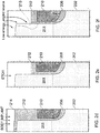
- the trench gate semiconductor device 300 may comprise a semiconductor layer 301 arranged on a semiconductor substrate 303.
- the semiconductor layer comprises an n-type drift region 302 formed on an n-type semiconductor substrate 303 which collectively form a drain region of the semiconductor device 300.
- a drain contact may be formed on the semiconductor substrate 303 by any appropriate means.
- a gate trench 305 is arranged to extend from a top portion of the semiconductor device 300 into the semiconductor layer 301, and terminating, in the drift region 302.
- a TBO 304 is formed in the bottom (or base) of the gate trench 305, a side wall oxide 318 is formed on the side walls of the gate trench 305, and gate dielectric 308 is formed at the top of the gate trench 305.
- the side wall oxide 318, trench bottom oxide (TBO) 304 and gate dielectric 308 collectively form a dielectric to electrically isolate a gate electrode 306.
- the gate electrode 306 is arranged in the gate trench 305 and is surrounded by the respective oxides 304, 308, 318.
- the semiconductor device 300 also comprises a p-type body region 311 which, excluding a source region 313 discussed below, extends from a top major surface of the device to a depth corresponding to the side walls of the gate trench 305.
- the body region 311 extends into the semiconductor device and terminates at or before the bottom of the gate trench 305.
- the body region 311 abuts the gate trench 305 along a length of the gate trench 305 starting at a point corresponding to the top of the gate electrode 306 and ending, as mentioned above, at or before the bottom of the gate trench 305.
- the body region 311 abuts a source region 313 at an upper portion thereof and abuts the gate trench 305 at a lower portion thereof. This allows for formation, by inversion, of the source to drain conduction channel of semiconductor device 300 during operation.
- the n-type source region 313 extends from the top surface of the semiconductor device 300, adjacent to the source contact area 312, and abuts the gate trench 305 along a length of the gate trench 305 from a point corresponding to a top surface of the gate dielectric 308 to a point corresponding a top surface of the gate electrode 306.
- the depth of the source region 313 into the semiconductor device 300 therefore corresponds to the thickness of a source metallisation 316 (discussed below) and the gate dielectric 308.
- the source region 313 thus extends to a depth of the gate trench 305 corresponding to a top surface of the gate electrode 306 .
- This arrangement results in a source region 313 which is aligned to the top surface of the gate electrode 306, which results in reduced dynamic gate charge (Qgs) and improves the switching performance of the devices leading, in turn to the trench-gate semiconductor device operating at lower temperature and higher efficiencies.
- Qgs dynamic gate charge
- the source metallisation 316 is thus arranged on the top surface of the gate dielectric 308 and is electrically connected the source region 313 and the body region 311 such that the source region 313 is aligned with the gate electrode 306.
- source contact is formed above the gate trench 305 of the semiconductor device 300.
- This allows for removal of conventional moat region configurations for contacting the source and body regions 311, 313.
- the skilled person will see that the arrangement of trench semiconductor device 300 according to the above described embodiments can achieve a higher density of active cells per unit area.
- contact to the gate polysilicon may be achieved by any appropriate means.
- the gate contact may be made by etching through the gate oxide into the gate electrode and forming appropriate metallisation therein.
Priority Applications (3)
| Application Number | Priority Date | Filing Date | Title |
|---|---|---|---|
| EP19154245.5A EP3690952A1 (fr) | 2019-01-29 | 2019-01-29 | Dispositif semiconducteur à grille à tranchée et son procédé de fabrication |
| CN202010070548.9A CN111490102A (zh) | 2019-01-29 | 2020-01-21 | 沟槽栅极半导体装置及其制造方法 |
| US16/774,436 US11222974B2 (en) | 2019-01-29 | 2020-01-28 | Trench gate semiconductor device and method of manufacture |
Applications Claiming Priority (1)
| Application Number | Priority Date | Filing Date | Title |
|---|---|---|---|
| EP19154245.5A EP3690952A1 (fr) | 2019-01-29 | 2019-01-29 | Dispositif semiconducteur à grille à tranchée et son procédé de fabrication |
Publications (1)
| Publication Number | Publication Date |
|---|---|
| EP3690952A1 true EP3690952A1 (fr) | 2020-08-05 |
Family
ID=65243418
Family Applications (1)
| Application Number | Title | Priority Date | Filing Date |
|---|---|---|---|
| EP19154245.5A Pending EP3690952A1 (fr) | 2019-01-29 | 2019-01-29 | Dispositif semiconducteur à grille à tranchée et son procédé de fabrication |
Country Status (3)
| Country | Link |
|---|---|
| US (1) | US11222974B2 (fr) |
| EP (1) | EP3690952A1 (fr) |
| CN (1) | CN111490102A (fr) |
Citations (3)
| Publication number | Priority date | Publication date | Assignee | Title |
|---|---|---|---|---|
| US20040209425A1 (en) * | 2003-04-03 | 2004-10-21 | Hirofumi Harada | Method of manufacturing a vertical MOS transistor |
| US20110133258A1 (en) * | 2009-08-14 | 2011-06-09 | Alpha And Omega Semiconductor Incorporated | Shielded gate trench mosfet with increased source-metal contact |
| US20130299898A1 (en) * | 2012-05-14 | 2013-11-14 | Freescale Semiconductor, Inc | Power mosfet structure and method |
Family Cites Families (15)
| Publication number | Priority date | Publication date | Assignee | Title |
|---|---|---|---|---|
| AT504289A2 (de) * | 2005-05-26 | 2008-04-15 | Fairchild Semiconductor | Trench-gate-feldeffekttransistoren und verfahren zum bilden derselben |
| US20080199995A1 (en) * | 2007-02-15 | 2008-08-21 | Debra Susan Woolsey | Integrated Hydrogen Anneal and Gate Oxidation for Improved Gate Oxide Integrity |
| US7956411B2 (en) * | 2008-01-15 | 2011-06-07 | Fairchild Semiconductor Corporation | High aspect ratio trench structures with void-free fill material |
| JP2009302510A (ja) * | 2008-03-03 | 2009-12-24 | Fuji Electric Device Technology Co Ltd | トレンチゲート型半導体装置およびその製造方法 |
| WO2011087994A2 (fr) * | 2010-01-12 | 2011-07-21 | Maxpower Semiconductor Inc. | Dispositifs, composants et procédés combinant des plaques de champ de tranchée avec charge électrostatique immobile |
| US8581341B2 (en) * | 2010-04-20 | 2013-11-12 | Maxpower Semiconductor, Inc. | Power MOSFET with embedded recessed field plate and methods of fabrication |
| JP6179409B2 (ja) * | 2014-01-24 | 2017-08-16 | 株式会社デンソー | 炭化珪素半導体装置の製造方法 |
| US20180366569A1 (en) * | 2016-06-10 | 2018-12-20 | Maxpower Semiconductor Inc. | Trench-Gated Heterostructure and Double-Heterostructure Active Devices |
| JP2018117070A (ja) * | 2017-01-19 | 2018-07-26 | エイブリック株式会社 | 半導体装置及びその製造方法 |
| JP6967352B2 (ja) * | 2017-02-07 | 2021-11-17 | ローム株式会社 | 半導体装置および半導体装置の製造方法、ならびに、半導体ウエハ構造物 |
| JP6817116B2 (ja) * | 2017-03-14 | 2021-01-20 | エイブリック株式会社 | 半導体装置 |
| JP2019114643A (ja) * | 2017-12-22 | 2019-07-11 | ルネサスエレクトロニクス株式会社 | 半導体装置およびその製造方法 |
| CN108172622A (zh) * | 2018-01-30 | 2018-06-15 | 电子科技大学 | 功率半导体器件 |
| DE102018130385A1 (de) * | 2018-11-29 | 2020-06-04 | Infineon Technologies Ag | Siliziumcarbid-Bauelemente, Halbleiterbauelemente und Verfahren zum Bilden von Siliziumcarbid-Bauelementen und Halbleiterbauelementen |
| US11658241B2 (en) * | 2018-12-31 | 2023-05-23 | Texas Instruments Incorporated | Vertical trench gate MOSFET with integrated Schottky diode |
-
2019
- 2019-01-29 EP EP19154245.5A patent/EP3690952A1/fr active Pending
-
2020
- 2020-01-21 CN CN202010070548.9A patent/CN111490102A/zh active Pending
- 2020-01-28 US US16/774,436 patent/US11222974B2/en active Active
Patent Citations (3)
| Publication number | Priority date | Publication date | Assignee | Title |
|---|---|---|---|---|
| US20040209425A1 (en) * | 2003-04-03 | 2004-10-21 | Hirofumi Harada | Method of manufacturing a vertical MOS transistor |
| US20110133258A1 (en) * | 2009-08-14 | 2011-06-09 | Alpha And Omega Semiconductor Incorporated | Shielded gate trench mosfet with increased source-metal contact |
| US20130299898A1 (en) * | 2012-05-14 | 2013-11-14 | Freescale Semiconductor, Inc | Power mosfet structure and method |
Also Published As
| Publication number | Publication date |
|---|---|
| CN111490102A (zh) | 2020-08-04 |
| US11222974B2 (en) | 2022-01-11 |
| US20200243679A1 (en) | 2020-07-30 |
Similar Documents
| Publication | Publication Date | Title |
|---|---|---|
| US10355125B2 (en) | Electrode contact structure for semiconductor device | |
| US9530883B2 (en) | Insulated gate semiconductor device having a shield electrode structure and method | |
| US9214545B2 (en) | Dual gate oxide trench MOSFET with channel stop trench | |
| US7361555B2 (en) | Trench-gate transistors and their manufacture | |
| US7868394B2 (en) | Metal-oxide-semiconductor transistor and method of manufacturing the same | |
| JP2662217B2 (ja) | 垂直ゲート半導体装置及びその製造方法 | |
| US7476589B2 (en) | Methods for forming shielded gate field effect transistors | |
| US20080142909A1 (en) | Ultra dense trench-gated power device with reduced drain source feedback capacitance and miller charge | |
| US6921699B2 (en) | Method for manufacturing a semiconductor device with a trench termination | |
| US20120326227A1 (en) | Method of making an insulated gate semiconductor device and structure | |
| CN105304692B (zh) | 用于在沟槽功率mosfet中优化端接设计的不对称多晶硅栅极的制备方法 | |
| US9837358B2 (en) | Source-gate region architecture in a vertical power semiconductor device | |
| JP2004522319A (ja) | ショットキー障壁を持つ半導体デバイスの製造 | |
| US8921184B2 (en) | Method of making an electrode contact structure and structure therefor | |
| US6639276B2 (en) | Power MOSFET with ultra-deep base and reduced on resistance | |
| US7557395B2 (en) | Trench MOSFET technology for DC-DC converter applications | |
| US11222974B2 (en) | Trench gate semiconductor device and method of manufacture | |
| CN113809162A (zh) | 功率元件 | |
| CN113690301B (zh) | 半导体器件及其制备方法 | |
| EP4362068A1 (fr) | Dispositif de transistor et procédé de fabrication de contacts sur un substrat semi-conducteur | |
| WO2021135342A1 (fr) | Dispositif semi-conducteur à oxyde de métal diffusé latéralement et son procédé de préparation | |
| CN115706155A (zh) | 带有屏蔽电极的底部源极沟槽mosfet |
Legal Events
| Date | Code | Title | Description |
|---|---|---|---|
| PUAI | Public reference made under article 153(3) epc to a published international application that has entered the european phase |
Free format text: ORIGINAL CODE: 0009012 |
|
| STAA | Information on the status of an ep patent application or granted ep patent |
Free format text: STATUS: THE APPLICATION HAS BEEN PUBLISHED |
|
| AK | Designated contracting states |
Kind code of ref document: A1 Designated state(s): AL AT BE BG CH CY CZ DE DK EE ES FI FR GB GR HR HU IE IS IT LI LT LU LV MC MK MT NL NO PL PT RO RS SE SI SK SM TR |
|
| AX | Request for extension of the european patent |
Extension state: BA ME |
|
| STAA | Information on the status of an ep patent application or granted ep patent |
Free format text: STATUS: REQUEST FOR EXAMINATION WAS MADE |
|
| 17P | Request for examination filed |
Effective date: 20210205 |
|
| RBV | Designated contracting states (corrected) |
Designated state(s): AL AT BE BG CH CY CZ DE DK EE ES FI FR GB GR HR HU IE IS IT LI LT LU LV MC MK MT NL NO PL PT RO RS SE SI SK SM TR |
|
| STAA | Information on the status of an ep patent application or granted ep patent |
Free format text: STATUS: EXAMINATION IS IN PROGRESS |
|
| 17Q | First examination report despatched |
Effective date: 20211110 |