EP3679644B1 - Schaltung und verfahren zur dämpfung von versorgungsspannungs-induzierten schwingungen im eingangskreis eines gleichspannungswandlers - Google Patents
Schaltung und verfahren zur dämpfung von versorgungsspannungs-induzierten schwingungen im eingangskreis eines gleichspannungswandlers Download PDFInfo
- Publication number
- EP3679644B1 EP3679644B1 EP18765705.1A EP18765705A EP3679644B1 EP 3679644 B1 EP3679644 B1 EP 3679644B1 EP 18765705 A EP18765705 A EP 18765705A EP 3679644 B1 EP3679644 B1 EP 3679644B1
- Authority
- EP
- European Patent Office
- Prior art keywords
- voltage
- connection
- circuit
- capacitor
- input circuit
- Prior art date
- Legal status (The legal status is an assumption and is not a legal conclusion. Google has not performed a legal analysis and makes no representation as to the accuracy of the status listed.)
- Active
Links
Images




Classifications
-
- H—ELECTRICITY
- H02—GENERATION; CONVERSION OR DISTRIBUTION OF ELECTRIC POWER
- H02M—APPARATUS FOR CONVERSION BETWEEN AC AND AC, BETWEEN AC AND DC, OR BETWEEN DC AND DC, AND FOR USE WITH MAINS OR SIMILAR POWER SUPPLY SYSTEMS; CONVERSION OF DC OR AC INPUT POWER INTO SURGE OUTPUT POWER; CONTROL OR REGULATION THEREOF
- H02M1/00—Details of apparatus for conversion
- H02M1/32—Means for protecting converters other than automatic disconnection
-
- H—ELECTRICITY
- H02—GENERATION; CONVERSION OR DISTRIBUTION OF ELECTRIC POWER
- H02M—APPARATUS FOR CONVERSION BETWEEN AC AND AC, BETWEEN AC AND DC, OR BETWEEN DC AND DC, AND FOR USE WITH MAINS OR SIMILAR POWER SUPPLY SYSTEMS; CONVERSION OF DC OR AC INPUT POWER INTO SURGE OUTPUT POWER; CONTROL OR REGULATION THEREOF
- H02M3/00—Conversion of DC power input into DC power output
- H02M3/02—Conversion of DC power input into DC power output without intermediate conversion into AC
- H02M3/04—Conversion of DC power input into DC power output without intermediate conversion into AC by static converters
- H02M3/10—Conversion of DC power input into DC power output without intermediate conversion into AC by static converters using discharge tubes with control electrode or semiconductor devices with control electrode
- H02M3/145—Conversion of DC power input into DC power output without intermediate conversion into AC by static converters using discharge tubes with control electrode or semiconductor devices with control electrode using devices of a triode or transistor type requiring continuous application of a control signal
- H02M3/155—Conversion of DC power input into DC power output without intermediate conversion into AC by static converters using discharge tubes with control electrode or semiconductor devices with control electrode using devices of a triode or transistor type requiring continuous application of a control signal using semiconductor devices only
- H02M3/156—Conversion of DC power input into DC power output without intermediate conversion into AC by static converters using discharge tubes with control electrode or semiconductor devices with control electrode using devices of a triode or transistor type requiring continuous application of a control signal using semiconductor devices only with automatic control of output voltage or current, e.g. switching regulators
- H02M3/158—Conversion of DC power input into DC power output without intermediate conversion into AC by static converters using discharge tubes with control electrode or semiconductor devices with control electrode using devices of a triode or transistor type requiring continuous application of a control signal using semiconductor devices only with automatic control of output voltage or current, e.g. switching regulators including plural semiconductor devices as final control devices for a single load
-
- G—PHYSICS
- G01—MEASURING; TESTING
- G01R—MEASURING ELECTRIC VARIABLES; MEASURING MAGNETIC VARIABLES
- G01R31/00—Arrangements for testing electric properties; Arrangements for locating electric faults; Arrangements for electrical testing characterised by what is being tested not provided for elsewhere
- G01R31/001—Measuring interference from external sources to, or emission from, the device under test, e.g. EMC, EMI, EMP or ESD testing
- G01R31/002—Measuring interference from external sources to, or emission from, the device under test, e.g. EMC, EMI, EMP or ESD testing where the device under test is an electronic circuit
-
- G—PHYSICS
- G01—MEASURING; TESTING
- G01R—MEASURING ELECTRIC VARIABLES; MEASURING MAGNETIC VARIABLES
- G01R31/00—Arrangements for testing electric properties; Arrangements for locating electric faults; Arrangements for electrical testing characterised by what is being tested not provided for elsewhere
- G01R31/12—Testing dielectric strength or breakdown voltage ; Testing or monitoring effectiveness or level of insulation, e.g. of a cable or of an apparatus, for example using partial discharge measurements; Electrostatic testing
- G01R31/14—Circuits therefor, e.g. for generating test voltages, sensing circuits
-
- H—ELECTRICITY
- H02—GENERATION; CONVERSION OR DISTRIBUTION OF ELECTRIC POWER
- H02M—APPARATUS FOR CONVERSION BETWEEN AC AND AC, BETWEEN AC AND DC, OR BETWEEN DC AND DC, AND FOR USE WITH MAINS OR SIMILAR POWER SUPPLY SYSTEMS; CONVERSION OF DC OR AC INPUT POWER INTO SURGE OUTPUT POWER; CONTROL OR REGULATION THEREOF
- H02M1/00—Details of apparatus for conversion
- H02M1/14—Arrangements for reducing ripples from DC input or output
- H02M1/15—Arrangements for reducing ripples from DC input or output using active elements
-
- H—ELECTRICITY
- H02—GENERATION; CONVERSION OR DISTRIBUTION OF ELECTRIC POWER
- H02M—APPARATUS FOR CONVERSION BETWEEN AC AND AC, BETWEEN AC AND DC, OR BETWEEN DC AND DC, AND FOR USE WITH MAINS OR SIMILAR POWER SUPPLY SYSTEMS; CONVERSION OF DC OR AC INPUT POWER INTO SURGE OUTPUT POWER; CONTROL OR REGULATION THEREOF
- H02M3/00—Conversion of DC power input into DC power output
- H02M3/02—Conversion of DC power input into DC power output without intermediate conversion into AC
- H02M3/04—Conversion of DC power input into DC power output without intermediate conversion into AC by static converters
- H02M3/06—Conversion of DC power input into DC power output without intermediate conversion into AC by static converters using resistors or capacitors, e.g. potential divider
- H02M3/07—Conversion of DC power input into DC power output without intermediate conversion into AC by static converters using resistors or capacitors, e.g. potential divider using capacitors charged and discharged alternately by semiconductor devices with control electrode, e.g. charge pumps
-
- H—ELECTRICITY
- H03—ELECTRONIC CIRCUITRY
- H03G—CONTROL OF AMPLIFICATION
- H03G11/00—Limiting amplitude; Limiting rate of change of amplitude
-
- H—ELECTRICITY
- H03—ELECTRONIC CIRCUITRY
- H03G—CONTROL OF AMPLIFICATION
- H03G1/00—Details of arrangements for controlling amplification
- H03G1/0005—Circuits characterised by the type of controlling devices operated by a controlling current or voltage signal
- H03G1/0035—Circuits characterised by the type of controlling devices operated by a controlling current or voltage signal using continuously variable impedance elements
-
- H—ELECTRICITY
- H03—ELECTRONIC CIRCUITRY
- H03G—CONTROL OF AMPLIFICATION
- H03G1/00—Details of arrangements for controlling amplification
- H03G1/0005—Circuits characterised by the type of controlling devices operated by a controlling current or voltage signal
- H03G1/0035—Circuits characterised by the type of controlling devices operated by a controlling current or voltage signal using continuously variable impedance elements
- H03G1/007—Circuits characterised by the type of controlling devices operated by a controlling current or voltage signal using continuously variable impedance elements using field-effect transistors [FET]
Definitions
- the present invention relates to a circuit and a method for damping / avoiding supply voltage-induced oscillations in an input circuit of a DC voltage converter during a surge voltage robustness test
- Fig. 1 the circuit diagram of an exemplary test setup (according to the state of the art) for impulse voltage tests is shown.
- the surge voltage amplitudes generated are typically between 0.5 kV and 6 kV.
- the surge generator used for the test has internal decoupling inductances that protect the test equipment and ensure that the surge voltage energy is concentrated in the direction of the test object (DUT, "device under test”). In connection with the negative differential input resistance and the input capacitance of a DC / DC converter, this can stimulate vibrations that make the test more difficult or damage the test item during the test.
- the pamphlets WO2011085703 , US2012313428 , US2006214599 and US6097158 suggest limiting the current in a feed line using FETs or MOSFETs as variable and controlled impedances.
- DE102010017303 describes an impulse voltage test system with a correction function to reduce systematic measurement errors.
- circuits according to the invention comprise an input circuit which sufficiently dampens vibrations occurring during the test by temporarily increasing the resistance of a semiconductor element arranged in the input circuit when voltage fluctuations occur.
- the voltage-dependent pinch-off property of a reverse polarity protection metal-oxide-semiconductor field effect transistor can be used by temporarily increasing the volume resistance of the MOSFET during a surge phase so that the resonant circuit (consisting of decoupling inductances of the surge generator, input capacitance and negative input resistance of the DC voltage converter) is damped.
- the degree of damping can also be adapted to the expected oscillation amplitude and frequency by adding resistors and capacitors.
- a test according to DIN EN 61000-4-5 is thus possible without significantly changing the test setup and without having to intervene or change the product and, in particular, without having to accept any restrictions with regard to the operating conditions.
- a circuit according to the invention comprises a DC voltage converter and an input circuit connected upstream of the DC voltage converter, which input circuit has a first connection and a second connection for connection to a voltage supply and a third connection and a fourth connection for connection to the DC voltage converter.
- the input circuit has a semiconductor element between the first and third connection, a first component connection of the semiconductor element being connected to a second component connection of the semiconductor element at least via a first capacitor and a second capacitor and a resistor of the semiconductor element being connected via a voltage between the first component connection and the second component connection is controllable.
- semiconductor element is to be understood in particular as an electronic component which is at least partially composed of Semiconductor material is made.
- DC voltage converter as used in the description and the claims is to be understood in particular as a circuit which converts a supplied DC voltage into a DC voltage with a higher, lower or inverted voltage level.
- the semiconductor element is preferably designed as a field effect transistor, FET, and preferably as a polarity reversal protection semiconductor switch.
- reverse polarity protection semiconductor switch as used in the description and the claims is to be understood in particular as a semiconductor element which interrupts the circuit when an electrical voltage of the wrong polarity is applied to the circuit.
- a gate connection of the FET is preferably connected to a first component connection of the first capacitor and connected to the source connection of the FET via a resistor of a voltage divider circuit connected in parallel with the first capacitor, a second component connection of the first capacitor and a second Component terminal of a second capacitor is connected to the second terminal and a source terminal of the FET is connected to a first component terminal of the second capacitor.
- the FET is preferably designed as a metal-oxide-semiconductor field effect transistor, MOSFET.
- the first connection is preferably connected to a first pole of the surge voltage generator and the second connection is connected to a second pole of the surge voltage generator, which has decoupling inductances.
- the first and second capacitors are preferably designed, an oscillation generated by applying a voltage to the DC voltage converter in an oscillating circuit comprising the decoupling inductances by increasing a voltage fluctuation-dependent To attenuate resistance of the semiconductor element, wherein the attenuation is designed to avoid an undervoltage shutdown of the DC voltage converter and / or an overload on an input protection diode.
- a method for testing a circuit for robustness against surge voltages comprises applying a voltage to an input circuit of the circuit, the input circuit having a semiconductor element, and damping an oscillation generated by the application of the voltage in the input circuit which causes a voltage fluctuation in the input circuit, wherein the attenuating comprises increasing a resistance of the semiconductor element in a controlled manner by the voltage fluctuation.
- the semiconductor element is preferably designed as a field effect transistor, FET, and particularly preferably as a polarity reversal protection semiconductor switch.
- the increase in resistance controlled by the voltage fluctuation preferably comprises a voltage fluctuation-dependent reduction of a gate-source voltage applied to the FET, which causes a time delay in a drop in a gate potential.
- a drain connection of the FET is preferably connected to a first pole of a voltage source and a gate connection of the FET is connected to a second pole of the voltage source via a capacitor, the time delay of the drop in the gate potential being caused by charging / discharging of the capacitor is effected via a resistor.
- Fig. 2 schematically illustrates a possible configuration of an input circuit 12 of a DC voltage converter (not shown).
- the input circuit 12 comprises a first connection 14 and a second connection 16 for connection to a voltage supply (for example 24 V).
- the input circuit 12 further comprises a third connection 18 and a fourth connection 20 for connection to the DC voltage converter.
- the first connection 14 is connected to the third connection 18 via the drain connection 22b and the source connection 22a of a semiconductor element 22 (FET or reverse polarity protection MOSFET).
- the gate terminal 22c is connected to the first terminal 14 and to the second terminal 16 via the voltage divider circuit 24, so that the gate potential (in quasi-stationary operation) is between the potential at the first terminal 14 and the potential at the second terminal 16 (and thus between the source potential and the ground potential). If the voltage difference between the first connection 14 and the second connection 16 is sufficiently high, the channel between the source connection 22a and the drain connection 22b becomes conductive. If the polarity of the first connection 14 and the second connection 16 is incorrect, the flow of current through the channel and the diode 26 is, however, prevented.
- an input protection diode circuit is arranged between the first connection 14 and the second connection 16 to limit the input voltage, which, for example, as in FIG Fig. 2 shown, may comprise two back-to-back connected Zener diodes.
- Fig. 3 shows a to the in Fig. 2 input circuit 12 shown and a DC voltage converter (not shown) connected to the input circuit 12, suitable start-up behavior when carrying out an impulse voltage test.
- the DC voltage converter After switching on the supplying test voltage (input voltage of the input circuit 10) 28, the DC voltage converter clocks the output voltage 32 from 0 V to 5 V from an input voltage 30 of 18 V.
- the capacitances in the input circuit 12 and the negative input resistance of the DC voltage converter Due to the decoupling inductances in the surge voltage generator 10, the capacitances in the input circuit 12 and the negative input resistance of the DC voltage converter, an increase in the input voltage 30 can be observed. In the negative half-cycle of the oscillation amplitude, the input voltage 30 falls below 12 V and thus below the undervoltage shutdown threshold of the DC voltage converter. As a result, the output voltage 32 of the DC voltage converter collapses and the test cannot be continued.
- a modified input circuit 34 for damping / avoiding such vibrations is in Fig. 4 shown.
- the input circuit 34 has, like the one in Fig. 2 input circuit 12 shown, a first connection 14 and a second Connection 16 for connection to a voltage supply and a third connection 18 and a fourth connection 20 for connection to the DC voltage converter (not shown).
- the first port 14 is as in FIG Fig. 2 , connected to the third connection 18 via the drain connection 22b and the source connection 22a of a reverse polarity protection MOSFET 22.
- the gate connection 22c is connected to the first connection 14 and to the second connection 16 via the voltage divider circuit 24, so that the gate potential 42 (in quasi-stationary operation) is between the potential at the first connection 14 and the potential at the second connection 16 (and thus between the source potential 40 and the ground potential).
- the gate terminal 22c of the reverse polarity protection MOSFET 22 is thus connected to the source terminal 22a of the reverse polarity protection MOSFET 22 via the first capacitor 36 and the second capacitor 38.
- an additional “discharge path” is generated between the source connection 22a and the gate connection 22c via the capacitors 36, 38.
- the source potential 40 drops when the oscillation amplitude changes from the positive to the negative half-cycle.
- the likewise falling gate potential 42 is supported by the first capacitor 36 to be discharged, whereby the gate potential 42 compared to the one in FIG Fig. 2 input circuit 12 shown drops more slowly.
- the voltage drop across the resistor R2 of the voltage divider circuit 24 is delayed by the time constant R1 * C1, whereby the voltage drop across R1 is accelerated.
- the input voltage 30 falls within one millisecond by 5 V, "sees" R2 in the same time a voltage drop of 1.8 V.
- the source-gate voltage 44 of the reverse polarity protection MOSFET 22 falls, as in FIG Fig. 5 shown, thus with approximately the same slope as the input voltage 30.
- the volume resistance of the reverse polarity protection MOSFET 22 acts in this area as a damping resistor in the LC resonant circuit.
- the attenuation is sufficient to keep the negative half-wave of the input voltage 30 above 20 V.
- the input voltage 30 of the DC / DC converter thus remains above the undervoltage shutdown threshold of 12 V, and the output voltage 32 of the DC / DC converter is consistently 5 V.
- the input circuit In normal operation (without test equipment with decoupling inductances) the input circuit is not influenced as desired.
- the reverse polarity protection MOSFET 22 could also be arranged between the second connection 16 and the fourth connection 20 instead of between the first connection 14 and the third connection 18.
- the reverse polarity protection MOSFET 22 instead of the reverse polarity protection MOSFET 22, other semiconductor elements whose contact resistance can be controlled via a voltage between two component connections can also be used, the use of FETs being only one possible embodiment of the teaching according to the invention.
- Fig. 7 shows a flow diagram of a method for testing a circuit for robustness against surge voltages.
- the method begins with a step 46 of applying a voltage to the input circuit 34 of the circuit.
- the application of the voltage includes, for example, as in Fig. 5 shown, an increase in the voltage between the first terminal 14 and the second terminal 16 from o V to a predetermined nominal value (z. B. 24 V).
- step 48 of damping an oscillation generated by the application of the voltage in the input circuit 34, which oscillation causes a voltage fluctuation in the input circuit 34.
- the attenuation serves to avoid a drop in the input voltage 30 below an undervoltage shutdown threshold of a device connected downstream of the input circuit 34 (e.g. a DC voltage converter) and to avoid reaching the input protection diode voltage.
- the attenuation includes, in particular, the temporary increase in the volume resistance of a semiconductor element arranged in the input circuit 34 when the input voltage 30 drops, for example by ensuring that the drop in the gate-source voltage compared to that in FIG Fig. 2
- the circuit 12 shown is accelerated, so that the source-drain path becomes highly resistive when the source potential 40 drops.
- the method concludes with step 50 of performing a surge voltage robustness test by applying a surge voltage to the input circuit 34.
Landscapes
- Engineering & Computer Science (AREA)
- Power Engineering (AREA)
- Physics & Mathematics (AREA)
- General Physics & Mathematics (AREA)
- Electromagnetism (AREA)
- Dc-Dc Converters (AREA)
Description
- Die vorliegende Erfindung bezieht sich auf eine Schaltung und ein Verfahren zur Dämpfung/Vermeidung von Versorgungsspannungs-induzierten Schwingungen in einem Eingangskreis eines Gleichspannungswandlers während einer Stoßspannungs-Robustheitsprüfung
- Die DIN EN 61000-4-5 fordert eine Prüfung und den Beweis der Robustheit elektrischer Geräte gegen Stoßspannungen (Surge) aus dem versorgenden Netz. In
Fig. 1 ist dazu das Schaltbild eines beispielhaften Prüfaufbaus (gemäß dem Stand der Technik) für Stoßspannungsprüfungen dargestellt. Die erzeugten Stoßspannungsamplituden liegen dabei typischerweise zwischen 0,5 kV und 6 kV. - Der für die Prüfung verwendete Surge-Generator weist interne Entkoppelungsinduktivitäten auf, die dem Schutz der Prüfeinrichtung dienen und dafür sorgen, dass die Stoßspannungsenergie in Richtung Prüfling (DUT, "device under test") konzentriert wird. In Verbindung mit dem negativen differenziellen Eingangswiderstand und der Eingangskapazität eines Gleichspannungswandlers können dadurch Schwingungen angeregt werden, die die Prüfung erschweren bzw. den Prüfling während der Prüfung beschädigen.
- Die Druckschriften
WO2011085703 ,US2012313428 ,US2006214599 undUS6097158 schlagen vor, den Strom in einer Zuleitung durch FETs oder MOSFETs als variable und gesteuerte Impedanzen zu begrenzen.DE102010017303 beschreibt ein Stoßspannungsprüfsystem mit einer Korrekturfunktion zur Reduzierung von systematischen Messfehlern. - Die Erfindung bereichert diesbezüglich den Stand der Technik, als erfindungsgemäße Schaltungen einen Eingangskreis umfassen, welcher bei der Prüfung entstehende Schwingungen hinreichend dämpft, indem der Widerstand eines im Eingangskreis angeordneten Halbleiterelements beim Auftreten von Spannungsschwankungen temporär erhöht wird.
- Bspw. kann die spannungsabhängige Abschnüreigenschaft eines Verpolungsschutz-Metall-Oxid-Halbleiter-Feldeffekttransistors (Verpolungsschutz-MOSFETs) genutzt werden, indem der Durchgangswiderstand des MOSFETs während einer Aufschwingphase temporär so erhöht wird, dass der Schwingkreis (bestehend aus Entkoppelungsinduktivitäten des Surge-Generators, Eingangskapazität und negativem Eingangswiderstand des Gleichspannungswandlers) bedämpft wird. Das Maß der Dämpfung kann zudem durch das Hinzufügen von Widerständen und Kondensatoren an die zu erwartende Schwingungsamplitude und an die zu erwartende Frequenz angepasst werden.
- Damit ist eine Prüfung nach DIN EN 61000-4-5 möglich, ohne den Testaufbau wesentlich zu ändern und ohne einen Eingriff bzw. eine Veränderung des Produkts vornehmen und insbesondere ohne Einschränkungen hinsichtlich der Betriebsbedingungen hinnehmen zu müssen.
- Die Erfindung wird durch die Merkmale der unabhängigen Ansprüche 1, 5 und 7 festgelegt. Die abhängigen Ansprüche definieren bevorzugte Ausgestaltungen der Erfindung.
- Eine erfindungsgemäße Schaltung umfasst einen Gleichspannungswandler und einen dem Gleichspannungswandler vorgeschalteten Eingangskreis, welcher einen ersten Anschluss und einen zweiten Anschluss zum Anschluss an eine Spannungsversorgung und einen dritten Anschluss und einen vierten Anschluss zum Anschluss an den Gleichspannungswandler aufweist.
- Der Eingangskreis weist zwischen dem ersten und dritten Anschluss ein Halbleiterelement auf, wobei ein erster Bauelemente-Anschluss des Halbleiterelements zumindest über einen ersten Kondensator und einen zweiten Kondensator an einen zweiten Bauelemente-Anschluss des Halbleiterelements angeschlossen ist und ein Widerstand des Halbleiterelements über eine Spannung zwischen dem ersten Bauelemente-Anschluss und dem zweiten Bauelemente-Anschluss steuerbar ist.
- Dabei ist unter dem Begriff "Halbleiterelement", wie er in der Beschreibung und den Ansprüchen verwendet wird, insbesondere ein elektronisches Bauelement zu verstehen, welches zumindest teilweise aus Halbleitermaterial hergestellt ist. Ferner ist unter dem Begriff "Gleichspannungswandler", wie er in der Beschreibung und den Ansprüchen verwendet wird, insbesondere eine Schaltung zu verstehen, die eine zugeführte Gleichspannung in eine Gleichspannung mit höherem, niedrigerem oder invertiertem Spannungsniveau umwandelt.
- Vorzugsweise ist das Halbleiterelement als Feldeffekttransistor, FET, und vorzugsweise als Verpolungsschutz-Halbleiterschalter ausgebildet.
- Dabei ist unter dem Begriff "Verpolungsschutz-Halbleiterschalter", wie er in der Beschreibung und den Ansprüchen verwendet wird, insbesondere ein Halbleiterelement zu verstehen, welches bei Anlegen einer elektrischen Spannung falscher Polarität an die Schaltung den Stromkreis unterbricht.
- Vorzugsweise ist ein Gate-Anschluss des FETs an einen ersten Bauelemente-Anschluss des ersten Kondensators angeschlossen und über einen Widerstand einer zum ersten Kondensator parallel geschalteten Spannungsteilerschaltung mit dem Source-Anschluss des FETs verbunden, sind ein zweiter Bauelemente-Anschluss des ersten Kondensators und ein zweiter Bauelemente-Anschluss eines zweiten Kondensators an dem zweiten Anschluss angeschlossen und ist ein Source-Anschluss des FETs an einen ersten Bauelemente-Anschluss des zweiten Kondensators angeschlossen..
- Vorzugsweise ist der FET als Metall-Oxid-Halbleiter-Feldeffekttransistor, MOSFET, ausgebildet.
- Vorzugsweise ist der erste Anschluss an einem ersten Pol des Stoßspannungs-Generators und der zweite Anschluss an einem zweiten Pol des Stoßspannungs-Generators, welcher Entkopplungs-Induktivitäten aufweist, angeschlossen.
- Vorzugsweise sind der erste und zweite Kondensator ausgebildet, eine durch Anlegen einer Spannung an den Gleichspannungswandler erzeugte Schwingung in einem die Entkopplungs-Induktivitäten umfassenden Schwingkreis durch spannungsschwankungsabhängiges Erhöhen eines Widerstands des Halbleiterelements zu dämpfen, wobei die Dämpfung ausgelegt ist, eine Unterspannungsabschaltung des Gleichspannungswandlers und/oder eine Überlast an einer Eingangsschutzdiode zu vermeiden.
- Ein erfindungsgemäßes Verfahren zur Prüfung einer Schaltung auf Robustheit gegen Stoßspannungen umfasst ein Anlegen einer Spannung an einen Eingangskreis der Schaltung, wobei der Eingangskreis ein Halbleiterelement aufweist, und ein Dämpfen einer durch das Anlegen der Spannung im Eingangskreis erzeugten Schwingung, welche im Eingangskreis eine Spannungsschwankung verursacht, wobei das Dämpfen ein durch die Spannungsschwankung gesteuertes Erhöhen eines Widerstandes des Halbleiterelements umfasst.
- Vorzugsweise ist das Halbleiterelement als Feldeffekttransistor, FET, und besonders vorzugsweise als Verpolungsschutz-Halbleiterschalter ausgebildet.
- Vorzugsweise umfasst das durch die Spannungsschwankung gesteuerte Erhöhen des Widerstandes ein spannungsschwankungsabhängiges Reduzieren einer am FET anliegenden Gate-Source-Spannung, welches ein zeitliches Verzögern eines Abfallens eines Gate-Potenzials bewirkt.
- Vorzugsweise ist ein Drain-Anschluss des FETs an einen ersten Pol einer Spannungsquelle angeschlossen und ein Gate-Anschluss des FETs über einen Kondensator mit einem zweiten Pol der Spannungsquelle verbunden, wobei das zeitliche Verzögern des Abfallens des Gate-Potenzials durch ein Aufladen/Entladen des Kondensators über einen Widerstand bewirkt wird.
- Die Erfindung wird nachfolgend in der detaillierten Beschreibung anhand von Ausführungsbeispielen erläutert, wobei auf Zeichnungen Bezug genommen wird, in denen:
-
Fig. 1 ein Schaltbild eines beispielhaften Prüfaufbaus (gemäß dem Stand der Technik) für eine Stoßspannungsprüfung; -
Fig. 2 ein Schaltbild eines einem Gleichspannungswandler vorschaltbaren Eingangskreises mit einem Verpolungsschutz und einem Filter für leitungsgebundene Störaussendung (gemäß dem Stand der Technik); -
Fig. 3 während einer Stoßspannungsprüfung im Eingangskreis derFig. 2 auftretende Schwingungen; -
Fig. 4 einen einem Gleichspannungswandler vorschaltbaren Eingangskreis zur Dämpfung/Vermeidung der Schwingungen; -
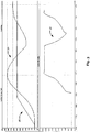
Fig. 5 während eines Robustheitstest im Eingangskreis derFig. 4 und am Ausgang eines dem Eingangskreis nachgeschalteten Gleichspannungswandlers auftretende Spannungen; -
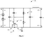
Fig. 6 einen im Vergleich zu dem inFig. 4 gezeigten Eingangskreis abgewandelten Eingangskreis; -
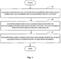
Fig. 7 ein Flussdiagramm eines Verfahrens zur Robustheitsprüfung einer Schaltung, die einen Gleichspannungswandler aufweist, zeigt. - Dabei sind in den Zeichnungen gleiche oder funktional ähnliche Elemente durch gleiche Bezugszeichen gekennzeichnet.
-
Fig. 2 illustriert schematisch eine mögliche Ausgestaltung eines Eingangskreises 12 eines Gleichspannungswandlers (nicht gezeigt). Der Eingangskreis 12 umfasst einen ersten Anschluss 14 und einen zweiten Anschluss 16 zum Anschluss an eine Spannungsversorgung (bspw. 24 V). Der Eingangskreis 12 umfasst ferner einen dritten Anschluss 18 und einen vierten Anschluss 20 zum Anschluss an den Gleichspannungswandler. Der erste Anschluss 14 ist über den Drain-Anschluss 22b und den Source-Anschluss 22a eines Halbleiterelements 22 (FET bzw. Verpolungsschutz-MOSFET) mit dem dritten Anschluss 18 verbunden. - Wie in
Fig. 2 gezeigt, ist der Gate-Anschluss 22c über die Spannungsteilerschaltung 24 an den ersten Anschluss 14 und an den zweiten Anschluss 16 angeschlossen, so dass das Gate-Potenzial (im quasistationären Betrieb) zwischen dem Potenzial am ersten Anschluss 14 und dem Potenzial am zweiten Anschluss 16 (und somit zwischen dem Source-Potenzial und dem Ground-Potenzial) liegt. Ist die Spannungsdifferenz zwischen dem ersten Anschluss 14 und dem zweiten Anschluss 16 ausreichend hoch, wird der Kanal zwischen dem Source-Anschluss 22a und dem Drain-Anschluss 22b leitend. Bei falscher Polung des ersten Anschluss 14 und des zweiten Anschluss 16, wird der Stromfluss durch den Kanal und die Diode 26 hingegen unterbunden. Zudem ist zwischen dem ersten Anschluss 14 und dem zweiten Anschluss 16 zur Begrenzung der Eingangsspannung eine Eingangsschutzdiodenschaltung angeordnet, welche bspw., wie inFig. 2 gezeigt, zwei antiseriell verschaltete Zenerdioden umfassen kann. -
Fig.3 zeigt ein zu dem inFig. 2 gezeigten Eingangskreis 12 und einem an den Eingangskreis 12 angeschlossenen Gleichspannungswandler (nicht gezeigt) passendes Anlaufverhalten bei Durchführung einer Stoßspannungsprüfung. Nach dem Einschalten der versorgenden Prüfspannung (Eingangsspannung des Eingangskreises 10) 28 taktet der Gleichspannungswandler ab einer Eingangsspannung 30 von 18 V die Ausgangsspannung 32 von o V auf 5 V hoch. - Aufgrund der Entkoppelungsinduktivitäten im Stoßspannungsgenerator 10, der Kapazitäten im Eingangskreis 12 und des negativen Eingangswiderstands des Gleichspannungswandlers ist ein Aufschwingen der Eingangsspannung 30 zu beobachten. In der negativen Halbwelle der Schwingungsamplitude fällt die Eingangsspannung 30 unter 12V und damit unter die Unterspannungsabschaltungsschwelle des Gleichspannungswandlers. In Folge dessen bricht die Ausgangsspannung 32 des Gleichspannungswandlers ein und die Prüfung kann nicht fortgesetzt werden.
- Ein modifizierter Eingangskreis 34 zur Dämpfung/Vermeidung solcher Schwingungen ist in
Fig. 4 gezeigt. Der Eingangskreis 34 weist, wie der inFig. 2 gezeigte Eingangskreis 12, einen ersten Anschluss 14 und einen zweiten Anschluss 16 zum Anschluss an eine Spannungsversorgung und einen dritten Anschluss 18 und einen vierten Anschluss 20 zum Anschluss an den Gleichspannungswandler (nicht gezeigt) auf. - Der erste Anschluss 14 ist, wie in
Fig. 2 , über den Drain-Anschluss 22b und den Source-Anschluss 22a eines Verpolungsschutz-MOSFETs 22 mit dem dritten Anschluss 18 verbunden. Ebenso ist der Gate-Anschluss 22c über die Spannungsteilerschaltung 24 an den ersten Anschluss 14 und an den zweiten Anschluss 16 angeschlossen, so dass das Gate-Potenzial 42 (im quasistationären Betrieb) zwischen dem Potenzial am ersten Anschluss 14 und dem Potenzial am zweiten Anschluss 16 (und somit zwischen dem Source-Potenzial 40 und dem Ground-Potenzial) liegt. - Jedoch ist der modifizierte Eingangskreis 34 im Vergleich zu dem in
Fig. 2 gezeigten Eingangskreis 12 um zwei Kondensatoren erweitert, einen ersten Kondensator 36 zwischen dem Gate-Anschluss 22c und dem zweiten Anschluss 16 und einen zweiten Kondensator 38 zwischen dem Source-Anschluss 22a und dem zweiten Anschluss 16. Wie inFig. 4 gezeigt, ist der Gate-Anschluss 22c des Verpolungsschutz-MOSFETs 22 somit über den ersten Kondensator 36 und den zweiten Kondensator 38 mit dem Source-Anschluss 22a des Verpolungsschutz-MOSFETs 22 verbunden. Dadurch wird über die Kondensatoren 36, 38 zwischen dem Source-Anschluss 22a und dem Gate-Anschluss 22c ein zusätzlicher "Entladepfad" erzeugt. - Wie in
Fig. 5 gezeigt, sinkt beim Übergang der Schwingungsamplitude von der positiven in die negative Halbwelle das Source-Potenzial 40. Jedoch wird das ebenfalls sinkende Gate-Potenzial 42 durch den zu entladenden ersten Kondensator 36 gestützt, wodurch das Gate-Potenzial 42 in Vergleich zu dem inFig. 2 gezeigten Eingangskreis 12 langsamer abfällt. - Anders ausgedrückt, wird der Spannungsabfall an dem Widerstand R2 der Spannungsteilerschaltung 24 durch die Zeitkonstante R1*C1 verzögert, wodurch der Spannungsabfall an R1 beschleunigt wird. Fällt z. B. die Eingangsspannung 30 innerhalb von einer Millisekunde um 5 V ab, "sieht" R2 in der gleichen Zeit einen Spannungsabfall von 1,8 V. Der Spannungsabfall an R1 beträgt dann: R1=5V-1,8V=3,2V.
- Wenn die Source-Gate-Spannung ursprünglich 5V betrug, so beträgt sie durch das Sinken der Eingangsspannung 30 nur noch 5 V-3,2 V = 1,8 V. Dadurch ist die Drain-Source Strecke deutlich hochohmiger geworden. Beim Übergang der Schwingungsamplitude von der positiven in die negative Halbwelle fällt die Source-Gate-Spannung 44 des Verpolungsschutz-MOSFETs 22, wie in
Fig. 5 gezeigt, somit annähernd mit der gleichen Steilheit wie die Eingangsspannung 30. - Dadurch wird die Source-Gate-Spannung reduziert und der Durchgangswiderstand des Verpolungsschutz-MOSFETs 22 zwischen dem Source-Anschluss 22a und dem Drain-Anschluss 22b erhöht. Durch das Erhöhen des Durchgangswiderstands des Verpolungsschutz-MOSFETs 22 wird der Abfall des Source-Potenzials gebremst, in Folge dessen sich die Source-Gate-Spannung 44 wieder stabilisiert.
- Dies bewirkt, dass sich der Durchgangswiderstand wieder reduziert und das Source-Potenzial erneut fällt. In
Fig. 5 ist dieses Verhalten an den welligen Abschnitten der Eingangsspannung 30 und der Source-Gate-Spannung 44 zu erkennen, die anzeigen, ab wann das Abschnürverhalten des Verpolungsschutz-MOSFETs 22 einsetzt (bzw. endet). - Der Durchgangswiderstand des Verpolungsschutz-MOSFETs 22 wirkt in diesem Bereich als ein Dämpfungswiderstand in dem LC-Schwingkreis. In dem in
Fig. 5 gezeigten Beispiel reicht die Dämpfung dabei aus, um die negative Halbwelle der Eingangsspannung 30 über 20 V zu halten. Damit bleibt die Eingangsspannung 30 des Gleichspannungswandlers über der Unterspannungsabschaltungsschwelle von 12 V, und die Ausgangsspannung 32 des Gleichspannungswandler beträgt durchgängig 5 V. - Somit kann eine Unterspannungsabschaltung des Gleichspannungswandlers vermieden und die Prüfung fortgesetzt werden. Sobald die Schwingung wieder in die positive Halbwelle übergeht, wird die Source-Gate-Spannung 44 wieder aufgeladen und der Durchgangswiderstand des Verpolungsschutz-MOSFETs 22 fällt. Die Intensität der Dämpfung lässt sich somit über eine geeignete Dimensionierung der Widerstände der Spannungsteilerschaltung 24 und der Kondensatoren 36, 38 auf die zu erwartenden Schwingungsfrequenzen und Amplituden einstellen.
- Im Normalbetrieb (ohne Prüfeinrichtung mit Entkoppelungsinduktivitäten) wird die Eingangsbeschaltung wie gewünscht nicht beeinflusst.
- Ferner versteht es sich, dass, wie in
Fig. 6 gezeigt, der Verpolungsschutz-MOSFET 22 anstatt zwischen dem ersten Anschluss 14 und dem dritten Anschluss 18 auch zwischen dem zweiten Anschluss 16 und dem vierten Anschluss 20 angeordnet sein könnte. Zudem versteht es sich, dass anstatt des Verpolungsschutz-MOSFETs 22 auch andere Halbleiterelemente, deren Durchgangswiderstand über eine Spannung zwischen zwei Bauelemente-Anschlüssen steuerbar ist, verwendet werden können, wobei die Verwendung von FETs nur eine mögliche Ausgestaltung der erfindungsgemäßen Lehre ist. -
Fig. 7 zeigt ein Flussdiagramm eines Verfahrens zur Prüfung einer Schaltung auf Robustheit gegen Stoßspannungen. Das Verfahren beginnt mit einem Schritt 46 des Anlegens einer Spannung an den Eingangskreis 34 der Schaltung. Das Anlegen der Spannung umfasst bspw., wie inFig. 5 gezeigt, ein Erhöhen der Spannung zwischen dem ersten Anschluss 14 und dem zweiten Anschluss 16 von o V auf einen vorbestimmten Nominalwert (z. B. 24 V). - Das Verfahren wird mit einem Schritt 48 des Dämpfens einer durch das Anlegen der Spannung im Eingangskreis 34 erzeugten Schwingung, welche im Eingangskreis 34 eine Spannungsschwankung verursacht, fortgesetzt. Wie in Zusammenhang mit
Fig. 3 und5 ausgeführt, dient die Dämpfung der Vermeidung eines Abfalls der Eingangsspannung 30 unter eine Unterspannungsabschaltungsschwelle eines dem Eingangskreis 34 nachgeschalteten Geräts (bspw. eines Gleichspannungswandlers) sowie der Vermeidung des Erreichens der Eingangsschutzdiodenspannung. - Die Dämpfung umfasst insbesondere das temporäre Erhöhen des Durchgangswiderstands eines im Eingangskreis 34 angeordneten Halbleiterelements, wenn die Eingangsspannung 30 abfällt, bspw. indem dafür gesorgt wird, dass der Abfall der Gate-Source-Spannung gegenüber der in
Fig. 2 gezeigten Schaltung 12 beschleunigt wird, so dass die Source-Drain-Strecke bei einem Abfallen des Source-Potenzials 40 hochohmig wird. - Das Verfahren schließt mit den Schritt 50 des Durchführens einer Stoßspannungs-Robustheitsprüfung durch Anlegen einer Stoßspannung an den Eingangskreis 34.
-
- 10
- Stoßspannungs-Generator
- 12
- Eingangskreis
- 14
- Anschluss
- 16
- Anschluss
- 18
- Anschluss
- 20
- Anschluss
- 22
- Halbleiterelement, FET, Verpolungsschutz-MOSFET
- 24
- Spannungsteilerschaltung
- 26
- Diode
- 28
- Eingangsspannung Eingangskreis
- 30
- Ausgangsspannung Eingangskreis
- 32
- Ausgangsspannung Gleichspannungswandler
- 34
- Modifizierter Eingangskreis
- 36
- Kondensator
- 38
- Kondensator
- 40
- Source-Potenzial
- 42
- Gate-Potenzials
- 44
- Source-Gate-Spannung
- 46
- Prozessschritt
- 48
- Prozessschritt
- 50
- Prozessschritt
Claims (10)
- Schaltung, umfassend:einen Gleichspannungswandler; undeinen dem Gleichspannungswandler vorgeschalteten Eingangskreis (34), welcher einen ersten Anschluss (14) und einen zweiten Anschluss (16) zum Anschluss an eine Spannungsversorgung und einen dritten Anschluss (18) und einen vierten Anschluss (20) zum Anschluss an den Gleichspannungswandler aufweist;wobei der Eingangskreis (34) zwischen dem ersten Anschluss (14) und dem dritten Anschluss (18) ein Halbleiterelement (22) aufweist, wobei ein erster Bauelemente-Anschluss (22c) des Halbleiterelements (22) zumindest über einen ersten Kondensator (36) und einen zweiten Kondensator (38) an einen zweiten Bauelemente-Anschluss (22a) des Halbleiterelements (22) angeschlossen ist, wobei der Eingangskreis (34) weiterhin aufweist:Mittel zum Steuern eines Durchgangswiderstands des Halbleiterelements (22) über eine Spannung zwischen dem ersten Bauelemente-Anschluss (22c) und dem zweiten Bauelemente-Anschluss (22a);Mittel zum Dämpfen (48) einer durch das Anlegen einer Spannung (28) im Eingangskreis (34) erzeugten Schwingung, welche bei einer Prüfung der Schaltung auf Robustheit gegen Stoßspannungen im Eingangskreis (34) entsteht und eine Spannungsschwankung verursacht, wobei das Dämpfen ein durch die Spannungsschwankung gesteuertes Erhöhen des Durchgangswiderstands des Halbleiterelements (22) umfasst;dadurch gekennzeichnet, dassder Eingangskreis eingerichtet ist, die Spannungsschwankung durch temporäres Erhöhen des Durchgangswiderstands in einer negativen Halbwelle der Schwingung zu dämpfen.
- Schaltung nach Anspruch 1, wobei das Halbleiterelement (22) als Feldeffekttransistor, FET, und vorzugsweise als Verpolungsschutz-Halbleiterschalter ausgebildet ist.
- Schaltung nach Anspruch 2, wobeiein Gate-Anschluss (22c) des FETs (22) an einen ersten Bauelemente-Anschluss des ersten Kondensators (36) angeschlossen ist und über einen Widerstand (R1) einer zum ersten Kondensator (36) parallel geschalteten Spannungsteilerschaltung (24) mit dem Source-Anschluss (22a) des FETs (22) verbunden ist;ein zweiter Bauelemente-Anschluss des ersten Kondensators (36) und ein zweiter Bauelemente-Anschluss eines zweiten Kondensators (38) an dem zweiten Anschluss angeschlossen sind; undein Source-Anschluss des FETs (22) an einen ersten Bauelemente-Anschluss des zweiten Kondensators (38) angeschlossen ist.
- Schaltung nach Anspruch 2 oder 3, wobei der FET (22) als Metall-Oxid-Halbleiter-Feldeffekttransistor, MOSFET, ausgebildet ist.
- System, umfassend:eine Schaltung nach einem der Ansprüche 1 bis 4; undeinen Stoßspannungs-Generator (10), welcher Entkopplungs-Induktivitäten aufweist; wobeider erste Anschluss (14) an einem ersten Pol des Stoßspannungs-Generators (10) und der zweite Anschluss (16) an einem zweiten Pol des Stoßspannungs-Generators (10) angeschlossen ist.
- System nach Anspruch 5, wobei der erste Kondensator (36) und der zweite Kondensator (38) ausgebildet sind, eine durch Anlegen einer Spannung an den Gleichspannungswandler erzeugte Schwingung in einem die Entkopplungs-Induktivitäten umfassenden Schwingkreis durch spannungsschwankungsabhängiges Erhöhen eines Widerstands des Halbleiterelements (22) zu dämpfen, wobei die Dämpfung ausgelegt ist, eine Unterspannungsabschaltung des Gleichspannungswandlers und/oder eine Überlast an einer Eingangsschutzdiode zu vermeiden.
- Verfahren zur Prüfung einer Schaltung nach Anspruch 1 auf Robustheit gegen Stoßspannungen, umfassend:Anlegen (46) einer Spannung (28) an einen Eingangskreis (34) der Schaltung, wobei der Eingangskreis (34) ein Halbleiterelement (22) aufweist; undDämpfen (48) einer durch das Anlegen der Spannung (28) im Eingangskreis (34) erzeugten Schwingung, welche im Eingangskreis (34) eine Spannungsschwankung verursacht;wobei das Dämpfen ein durch die Spannungsschwankung gesteuertes Erhöhen eines Widerstandes des Halbleiterelements (22) umfasst;dadurch gekennzeichnet, dassdie Spannungsschwankung durch temporäres Erhöhen des Durchgangswiderstands in einer negativen Halbwelle der Schwingung gedämpft wird.
- Verfahren nach Anspruch 7, wobei das Halbleiterelement (22) als Feldeffekttransistor, FET, und vorzugsweise als Verpolungsschutz-Halbleiterschalter ausgebildet ist.
- Verfahren nach Anspruch 8, wobei das durch die Spannungsschwankung gesteuerte Erhöhen des Widerstandes ein spannungsschwankungsabhängiges Reduzieren einer am FET (22) anliegenden Gate-Source-Spannung umfasst.
- Verfahren nach Anspruch 9, wobeiein Drain-Anschluss (22b) des FETs (22) an einen ersten Pol einer Spannungsquelle angeschlossen ist; undein Gate-Anschluss (22c) des FETs (22) über einen Kondensator (36) mit einem zweiten Pol der Spannungsquelle verbunden ist;wobei eine zeitliche Beschleunigung des Abfallens des Gate-Potenzials (42) durch ein Entladen des Kondensators (36) über einen Widerstand (R1)bewirkt wird.
Applications Claiming Priority (2)
| Application Number | Priority Date | Filing Date | Title |
|---|---|---|---|
| DE202017004715.2U DE202017004715U1 (de) | 2017-09-08 | 2017-09-08 | Schaltung zur Dämpfung von Versorgungsspannungsinduzierten Schwingungen im Eingangskreis eines Gleichspannungswandlers |
| PCT/IB2018/000816 WO2019048919A1 (de) | 2017-09-08 | 2018-07-30 | Schaltung und verfahren zur dämpfung von versorgungsspannungs-induzierten schwingungen im eingangskreis eines gleichspannungswandlers |
Publications (2)
| Publication Number | Publication Date |
|---|---|
| EP3679644A1 EP3679644A1 (de) | 2020-07-15 |
| EP3679644B1 true EP3679644B1 (de) | 2021-09-01 |
Family
ID=63517921
Family Applications (1)
| Application Number | Title | Priority Date | Filing Date |
|---|---|---|---|
| EP18765705.1A Active EP3679644B1 (de) | 2017-09-08 | 2018-07-30 | Schaltung und verfahren zur dämpfung von versorgungsspannungs-induzierten schwingungen im eingangskreis eines gleichspannungswandlers |
Country Status (5)
| Country | Link |
|---|---|
| US (1) | US11152858B2 (de) |
| EP (1) | EP3679644B1 (de) |
| CN (1) | CN111033991B (de) |
| DE (1) | DE202017004715U1 (de) |
| WO (1) | WO2019048919A1 (de) |
Cited By (2)
| Publication number | Priority date | Publication date | Assignee | Title |
|---|---|---|---|---|
| TWI860817B (zh) * | 2023-08-18 | 2024-11-01 | 台達電子工業股份有限公司 | 可抑制湧浪電流的開關觸發器 |
| US12489367B2 (en) | 2023-08-18 | 2025-12-02 | Delta Electronics, Inc. | Switch trigger for suppressing inrush current |
Families Citing this family (1)
| Publication number | Priority date | Publication date | Assignee | Title |
|---|---|---|---|---|
| DE102018010126B3 (de) | 2018-12-24 | 2020-05-07 | Leopold Kostal Gmbh & Co. Kg | Verpolschutzschaltung |
Family Cites Families (16)
| Publication number | Priority date | Publication date | Assignee | Title |
|---|---|---|---|---|
| US4631470A (en) * | 1985-12-13 | 1986-12-23 | Rca Corporation | Current surge limited power supply |
| US4843515A (en) * | 1987-04-20 | 1989-06-27 | Keytek Instrument Corp. | Surge undershoot eliminator |
| JPH07288981A (ja) * | 1994-04-14 | 1995-10-31 | Fuji Electric Co Ltd | 定電圧装置 |
| IL120983A (en) * | 1997-06-03 | 2003-04-10 | Lightech Electronics Ind Ltd | Low voltage illumination system |
| US6611410B1 (en) * | 1999-12-17 | 2003-08-26 | Siemens Vdo Automotive Inc. | Positive supply lead reverse polarity protection circuit |
| US6898092B2 (en) * | 2003-06-25 | 2005-05-24 | Picor Corporation | EMI filter circuit |
| JP3113228U (ja) * | 2005-06-01 | 2005-09-02 | 船井電機株式会社 | プラズマテレビジョン |
| TWI340519B (en) * | 2006-10-03 | 2011-04-11 | Wistron Corp | Regulated device of a dc power supply, fuel cell, and portable electronic device using a fuel cell |
| CN201256290Y (zh) * | 2008-08-04 | 2009-06-10 | 研祥智能科技股份有限公司 | 一种抑制浪涌电流和防输入电压反接的保护电路 |
| RU2518908C2 (ru) * | 2010-01-12 | 2014-06-10 | Гира Гирзипен Гмбх Унд Ко. Кг | Устройство для обеспечения напряжения питания в шинном узле шинной сети |
| DE102010017303A1 (de) * | 2010-02-05 | 2011-08-11 | Hinow, Georg, Dr. Ing., 01279 | Stoßspannungsprüfsystem mit einem Messsignalauswertegerät mit einem Korrekturalgorithmus |
| JP2011171834A (ja) * | 2010-02-16 | 2011-09-01 | Panasonic Electric Works Co Ltd | 通信システムおよび電子チョーク回路 |
| JP2014090316A (ja) * | 2012-10-30 | 2014-05-15 | Juki Corp | ゲート駆動回路 |
| JP2016136793A (ja) * | 2013-05-14 | 2016-07-28 | シャープ株式会社 | スイッチング電源装置と、それを用いたインバータ、コンバータ、およびソーラーパワーコントローラ |
| CN103944549A (zh) * | 2014-04-03 | 2014-07-23 | 南京航空航天大学 | 一种高可靠性mosfet驱动电路 |
| US9647558B2 (en) * | 2014-05-02 | 2017-05-09 | Intersil Americas LLC | System and method for maintaining a constant output voltage ripple in a buck converter in discontinuous conduction mode |
-
2017
- 2017-09-08 DE DE202017004715.2U patent/DE202017004715U1/de active Active
-
2018
- 2018-07-30 CN CN201880054986.7A patent/CN111033991B/zh active Active
- 2018-07-30 EP EP18765705.1A patent/EP3679644B1/de active Active
- 2018-07-30 WO PCT/IB2018/000816 patent/WO2019048919A1/de not_active Ceased
-
2020
- 2020-03-09 US US16/813,256 patent/US11152858B2/en active Active
Cited By (2)
| Publication number | Priority date | Publication date | Assignee | Title |
|---|---|---|---|---|
| TWI860817B (zh) * | 2023-08-18 | 2024-11-01 | 台達電子工業股份有限公司 | 可抑制湧浪電流的開關觸發器 |
| US12489367B2 (en) | 2023-08-18 | 2025-12-02 | Delta Electronics, Inc. | Switch trigger for suppressing inrush current |
Also Published As
| Publication number | Publication date |
|---|---|
| US11152858B2 (en) | 2021-10-19 |
| WO2019048919A1 (de) | 2019-03-14 |
| CN111033991A (zh) | 2020-04-17 |
| CN111033991B (zh) | 2024-05-10 |
| US20200212803A1 (en) | 2020-07-02 |
| EP3679644A1 (de) | 2020-07-15 |
| DE202017004715U1 (de) | 2018-12-11 |
Similar Documents
| Publication | Publication Date | Title |
|---|---|---|
| DE112016000392B4 (de) | Signalübertragungs-Einrichtung | |
| DE69128967T2 (de) | Schaltungsschutzeinrichtung | |
| EP3021444B1 (de) | Schaltung zum schutz vor überspannungen | |
| DE69122541T2 (de) | Statischer Schalter für mittlere Spannung | |
| DE10235444B4 (de) | Treibersteuerungseinrichtung, Leistungsumformungseinrichtung, Verfahren zur Steuerung einer Leistungsumformungseinrichtung und Verfahren zum Gebrauch einer Leistungsumformungseinrichtung | |
| DE102013219475B4 (de) | Elektronischer schaltkreis mit einem elektronischenschalter und einem überwachungsschaltkreis | |
| DE102009022832A1 (de) | Mehrstufige Überspannungsschutzschaltung, insbesondere für informationstechnische Anlagen | |
| WO2012079570A2 (de) | Schaltung zum schutz eines elektrischen verbrauchers gegen überspannungen | |
| DE102022113118A1 (de) | Dynamisches Schalten von Ladungspumpen mit Divisionsverhältnis | |
| DE102018123509A1 (de) | Spannungspegelumsetzerschaltung und Verfahren | |
| DE102014107815A1 (de) | System und Verfahren zum Ansteuern von Transistoren | |
| DE202016104258U1 (de) | Integrierte Schaltsteuerung von Anti-Serienschaltern | |
| WO2019048919A1 (de) | Schaltung und verfahren zur dämpfung von versorgungsspannungs-induzierten schwingungen im eingangskreis eines gleichspannungswandlers | |
| DE112017004130T5 (de) | Verfahren und Systeme zum Reduzieren von Ladungspumpensubstratrauschen | |
| EP1095453B1 (de) | Schaltungsanordnung zum ansteuern einer schaltvorrichtung zum schalten eines elektrischen verbrauchers | |
| DE10223996B4 (de) | Referenzspannungsschaltung und Verfahren zum Erzeugen einer Referenzspannung | |
| DE102005002359B4 (de) | Schaltung zur Strombegrenzung und Verfahren zum Betrieb der Schaltung | |
| DE102014113715A1 (de) | Eine Schutzschaltung für den Schutz elektronischer Steuerungen vor transienten Automobil-Überspannungsimpulsen | |
| DE102007018237B4 (de) | Schaltung mit verbessertem ESD-Schutz bei repetierender Pulsbelastung | |
| DE102016218598B4 (de) | Vorrichtung und Verfahren für einen ESD-Schutz eines Halbleiters | |
| DE69322934T2 (de) | Vorrichtung mit einer Schaltung zum Verarbeiten eines Wechselsignals | |
| WO2018019869A1 (de) | Verfahren und vorrichtung zur ansteuerung eines halbleiterschalters | |
| EP3053270B1 (de) | Invertschaltung mit spannungsbegrenzung | |
| EP0992114B1 (de) | Ansteuerschaltung für ein steuerbares halbleiterbauelement | |
| EP1078460A1 (de) | Verfahren und vorrichtung zum umschalten eines feldeffekttransistors |
Legal Events
| Date | Code | Title | Description |
|---|---|---|---|
| STAA | Information on the status of an ep patent application or granted ep patent |
Free format text: STATUS: UNKNOWN |
|
| STAA | Information on the status of an ep patent application or granted ep patent |
Free format text: STATUS: THE INTERNATIONAL PUBLICATION HAS BEEN MADE |
|
| PUAI | Public reference made under article 153(3) epc to a published international application that has entered the european phase |
Free format text: ORIGINAL CODE: 0009012 |
|
| STAA | Information on the status of an ep patent application or granted ep patent |
Free format text: STATUS: REQUEST FOR EXAMINATION WAS MADE |
|
| 17P | Request for examination filed |
Effective date: 20200225 |
|
| AK | Designated contracting states |
Kind code of ref document: A1 Designated state(s): AL AT BE BG CH CY CZ DE DK EE ES FI FR GB GR HR HU IE IS IT LI LT LU LV MC MK MT NL NO PL PT RO RS SE SI SK SM TR |
|
| AX | Request for extension of the european patent |
Extension state: BA ME |
|
| DAV | Request for validation of the european patent (deleted) | ||
| DAX | Request for extension of the european patent (deleted) | ||
| GRAP | Despatch of communication of intention to grant a patent |
Free format text: ORIGINAL CODE: EPIDOSNIGR1 |
|
| STAA | Information on the status of an ep patent application or granted ep patent |
Free format text: STATUS: GRANT OF PATENT IS INTENDED |
|
| INTG | Intention to grant announced |
Effective date: 20210406 |
|
| GRAS | Grant fee paid |
Free format text: ORIGINAL CODE: EPIDOSNIGR3 |
|
| GRAA | (expected) grant |
Free format text: ORIGINAL CODE: 0009210 |
|
| STAA | Information on the status of an ep patent application or granted ep patent |
Free format text: STATUS: THE PATENT HAS BEEN GRANTED |
|
| AK | Designated contracting states |
Kind code of ref document: B1 Designated state(s): AL AT BE BG CH CY CZ DE DK EE ES FI FR GB GR HR HU IE IS IT LI LT LU LV MC MK MT NL NO PL PT RO RS SE SI SK SM TR |
|
| REG | Reference to a national code |
Ref country code: GB Ref legal event code: FG4D Free format text: NOT ENGLISH |
|
| REG | Reference to a national code |
Ref country code: CH Ref legal event code: EP Ref country code: AT Ref legal event code: REF Ref document number: 1427270 Country of ref document: AT Kind code of ref document: T Effective date: 20210915 |
|
| REG | Reference to a national code |
Ref country code: DE Ref legal event code: R096 Ref document number: 502018006882 Country of ref document: DE |
|
| REG | Reference to a national code |
Ref country code: IE Ref legal event code: FG4D Free format text: LANGUAGE OF EP DOCUMENT: GERMAN |
|
| REG | Reference to a national code |
Ref country code: LT Ref legal event code: MG9D |
|
| REG | Reference to a national code |
Ref country code: NL Ref legal event code: MP Effective date: 20210901 |
|
| PG25 | Lapsed in a contracting state [announced via postgrant information from national office to epo] |
Ref country code: RS Free format text: LAPSE BECAUSE OF FAILURE TO SUBMIT A TRANSLATION OF THE DESCRIPTION OR TO PAY THE FEE WITHIN THE PRESCRIBED TIME-LIMIT Effective date: 20210901 Ref country code: SE Free format text: LAPSE BECAUSE OF FAILURE TO SUBMIT A TRANSLATION OF THE DESCRIPTION OR TO PAY THE FEE WITHIN THE PRESCRIBED TIME-LIMIT Effective date: 20210901 Ref country code: BG Free format text: LAPSE BECAUSE OF FAILURE TO SUBMIT A TRANSLATION OF THE DESCRIPTION OR TO PAY THE FEE WITHIN THE PRESCRIBED TIME-LIMIT Effective date: 20211201 Ref country code: LT Free format text: LAPSE BECAUSE OF FAILURE TO SUBMIT A TRANSLATION OF THE DESCRIPTION OR TO PAY THE FEE WITHIN THE PRESCRIBED TIME-LIMIT Effective date: 20210901 Ref country code: NO Free format text: LAPSE BECAUSE OF FAILURE TO SUBMIT A TRANSLATION OF THE DESCRIPTION OR TO PAY THE FEE WITHIN THE PRESCRIBED TIME-LIMIT Effective date: 20211201 Ref country code: ES Free format text: LAPSE BECAUSE OF FAILURE TO SUBMIT A TRANSLATION OF THE DESCRIPTION OR TO PAY THE FEE WITHIN THE PRESCRIBED TIME-LIMIT Effective date: 20210901 Ref country code: FI Free format text: LAPSE BECAUSE OF FAILURE TO SUBMIT A TRANSLATION OF THE DESCRIPTION OR TO PAY THE FEE WITHIN THE PRESCRIBED TIME-LIMIT Effective date: 20210901 Ref country code: HR Free format text: LAPSE BECAUSE OF FAILURE TO SUBMIT A TRANSLATION OF THE DESCRIPTION OR TO PAY THE FEE WITHIN THE PRESCRIBED TIME-LIMIT Effective date: 20210901 |
|
| PG25 | Lapsed in a contracting state [announced via postgrant information from national office to epo] |
Ref country code: PL Free format text: LAPSE BECAUSE OF FAILURE TO SUBMIT A TRANSLATION OF THE DESCRIPTION OR TO PAY THE FEE WITHIN THE PRESCRIBED TIME-LIMIT Effective date: 20210901 Ref country code: LV Free format text: LAPSE BECAUSE OF FAILURE TO SUBMIT A TRANSLATION OF THE DESCRIPTION OR TO PAY THE FEE WITHIN THE PRESCRIBED TIME-LIMIT Effective date: 20210901 Ref country code: GR Free format text: LAPSE BECAUSE OF FAILURE TO SUBMIT A TRANSLATION OF THE DESCRIPTION OR TO PAY THE FEE WITHIN THE PRESCRIBED TIME-LIMIT Effective date: 20211202 |
|
| PG25 | Lapsed in a contracting state [announced via postgrant information from national office to epo] |
Ref country code: IS Free format text: LAPSE BECAUSE OF FAILURE TO SUBMIT A TRANSLATION OF THE DESCRIPTION OR TO PAY THE FEE WITHIN THE PRESCRIBED TIME-LIMIT Effective date: 20220101 Ref country code: SM Free format text: LAPSE BECAUSE OF FAILURE TO SUBMIT A TRANSLATION OF THE DESCRIPTION OR TO PAY THE FEE WITHIN THE PRESCRIBED TIME-LIMIT Effective date: 20210901 Ref country code: SK Free format text: LAPSE BECAUSE OF FAILURE TO SUBMIT A TRANSLATION OF THE DESCRIPTION OR TO PAY THE FEE WITHIN THE PRESCRIBED TIME-LIMIT Effective date: 20210901 Ref country code: RO Free format text: LAPSE BECAUSE OF FAILURE TO SUBMIT A TRANSLATION OF THE DESCRIPTION OR TO PAY THE FEE WITHIN THE PRESCRIBED TIME-LIMIT Effective date: 20210901 Ref country code: PT Free format text: LAPSE BECAUSE OF FAILURE TO SUBMIT A TRANSLATION OF THE DESCRIPTION OR TO PAY THE FEE WITHIN THE PRESCRIBED TIME-LIMIT Effective date: 20220103 Ref country code: NL Free format text: LAPSE BECAUSE OF FAILURE TO SUBMIT A TRANSLATION OF THE DESCRIPTION OR TO PAY THE FEE WITHIN THE PRESCRIBED TIME-LIMIT Effective date: 20210901 Ref country code: EE Free format text: LAPSE BECAUSE OF FAILURE TO SUBMIT A TRANSLATION OF THE DESCRIPTION OR TO PAY THE FEE WITHIN THE PRESCRIBED TIME-LIMIT Effective date: 20210901 Ref country code: CZ Free format text: LAPSE BECAUSE OF FAILURE TO SUBMIT A TRANSLATION OF THE DESCRIPTION OR TO PAY THE FEE WITHIN THE PRESCRIBED TIME-LIMIT Effective date: 20210901 Ref country code: AL Free format text: LAPSE BECAUSE OF FAILURE TO SUBMIT A TRANSLATION OF THE DESCRIPTION OR TO PAY THE FEE WITHIN THE PRESCRIBED TIME-LIMIT Effective date: 20210901 |
|
| REG | Reference to a national code |
Ref country code: DE Ref legal event code: R097 Ref document number: 502018006882 Country of ref document: DE |
|
| PLBE | No opposition filed within time limit |
Free format text: ORIGINAL CODE: 0009261 |
|
| STAA | Information on the status of an ep patent application or granted ep patent |
Free format text: STATUS: NO OPPOSITION FILED WITHIN TIME LIMIT |
|
| PG25 | Lapsed in a contracting state [announced via postgrant information from national office to epo] |
Ref country code: DK Free format text: LAPSE BECAUSE OF FAILURE TO SUBMIT A TRANSLATION OF THE DESCRIPTION OR TO PAY THE FEE WITHIN THE PRESCRIBED TIME-LIMIT Effective date: 20210901 |
|
| 26N | No opposition filed |
Effective date: 20220602 |
|
| PG25 | Lapsed in a contracting state [announced via postgrant information from national office to epo] |
Ref country code: SI Free format text: LAPSE BECAUSE OF FAILURE TO SUBMIT A TRANSLATION OF THE DESCRIPTION OR TO PAY THE FEE WITHIN THE PRESCRIBED TIME-LIMIT Effective date: 20210901 |
|
| PG25 | Lapsed in a contracting state [announced via postgrant information from national office to epo] |
Ref country code: MC Free format text: LAPSE BECAUSE OF FAILURE TO SUBMIT A TRANSLATION OF THE DESCRIPTION OR TO PAY THE FEE WITHIN THE PRESCRIBED TIME-LIMIT Effective date: 20210901 |
|
| GBPC | Gb: european patent ceased through non-payment of renewal fee |
Effective date: 20220730 |
|
| REG | Reference to a national code |
Ref country code: BE Ref legal event code: MM Effective date: 20220731 |
|
| PG25 | Lapsed in a contracting state [announced via postgrant information from national office to epo] |
Ref country code: LU Free format text: LAPSE BECAUSE OF NON-PAYMENT OF DUE FEES Effective date: 20220730 |
|
| PG25 | Lapsed in a contracting state [announced via postgrant information from national office to epo] |
Ref country code: GB Free format text: LAPSE BECAUSE OF NON-PAYMENT OF DUE FEES Effective date: 20220730 Ref country code: BE Free format text: LAPSE BECAUSE OF NON-PAYMENT OF DUE FEES Effective date: 20220731 |
|
| P01 | Opt-out of the competence of the unified patent court (upc) registered |
Effective date: 20230516 |
|
| PG25 | Lapsed in a contracting state [announced via postgrant information from national office to epo] |
Ref country code: IE Free format text: LAPSE BECAUSE OF NON-PAYMENT OF DUE FEES Effective date: 20220730 |
|
| PG25 | Lapsed in a contracting state [announced via postgrant information from national office to epo] |
Ref country code: MK Free format text: LAPSE BECAUSE OF FAILURE TO SUBMIT A TRANSLATION OF THE DESCRIPTION OR TO PAY THE FEE WITHIN THE PRESCRIBED TIME-LIMIT Effective date: 20210901 Ref country code: CY Free format text: LAPSE BECAUSE OF FAILURE TO SUBMIT A TRANSLATION OF THE DESCRIPTION OR TO PAY THE FEE WITHIN THE PRESCRIBED TIME-LIMIT Effective date: 20210901 |
|
| PG25 | Lapsed in a contracting state [announced via postgrant information from national office to epo] |
Ref country code: HU Free format text: LAPSE BECAUSE OF FAILURE TO SUBMIT A TRANSLATION OF THE DESCRIPTION OR TO PAY THE FEE WITHIN THE PRESCRIBED TIME-LIMIT; INVALID AB INITIO Effective date: 20180730 |
|
| PG25 | Lapsed in a contracting state [announced via postgrant information from national office to epo] |
Ref country code: MT Free format text: LAPSE BECAUSE OF FAILURE TO SUBMIT A TRANSLATION OF THE DESCRIPTION OR TO PAY THE FEE WITHIN THE PRESCRIBED TIME-LIMIT Effective date: 20210901 |
|
| PGFP | Annual fee paid to national office [announced via postgrant information from national office to epo] |
Ref country code: DE Payment date: 20250728 Year of fee payment: 8 |
|
| PGFP | Annual fee paid to national office [announced via postgrant information from national office to epo] |
Ref country code: IT Payment date: 20250721 Year of fee payment: 8 |
|
| PGFP | Annual fee paid to national office [announced via postgrant information from national office to epo] |
Ref country code: FR Payment date: 20250725 Year of fee payment: 8 Ref country code: AT Payment date: 20250718 Year of fee payment: 8 |
|
| PGFP | Annual fee paid to national office [announced via postgrant information from national office to epo] |
Ref country code: CH Payment date: 20250801 Year of fee payment: 8 |
|
| PG25 | Lapsed in a contracting state [announced via postgrant information from national office to epo] |
Ref country code: TR Free format text: LAPSE BECAUSE OF FAILURE TO SUBMIT A TRANSLATION OF THE DESCRIPTION OR TO PAY THE FEE WITHIN THE PRESCRIBED TIME-LIMIT Effective date: 20210901 |