EP3675153A1 - Verfahren zum herstellen eines substratadapters und substratadapter zum verbinden mit einem elektronikbauteil - Google Patents
Verfahren zum herstellen eines substratadapters und substratadapter zum verbinden mit einem elektronikbauteil Download PDFInfo
- Publication number
- EP3675153A1 EP3675153A1 EP19196401.4A EP19196401A EP3675153A1 EP 3675153 A1 EP3675153 A1 EP 3675153A1 EP 19196401 A EP19196401 A EP 19196401A EP 3675153 A1 EP3675153 A1 EP 3675153A1
- Authority
- EP
- European Patent Office
- Prior art keywords
- material layer
- substrate
- contacting material
- carrier
- contacting
- Prior art date
- Legal status (The legal status is an assumption and is not a legal conclusion. Google has not performed a legal analysis and makes no representation as to the accuracy of the status listed.)
- Pending
Links
Images
Classifications
-
- H—ELECTRICITY
- H10—SEMICONDUCTOR DEVICES; ELECTRIC SOLID-STATE DEVICES NOT OTHERWISE PROVIDED FOR
- H10W—GENERIC PACKAGES, INTERCONNECTIONS, CONNECTORS OR OTHER CONSTRUCTIONAL DETAILS OF DEVICES COVERED BY CLASS H10
- H10W72/00—Interconnections or connectors in packages
- H10W72/01—Manufacture or treatment
- H10W72/013—Manufacture or treatment of die-attach connectors
-
- H—ELECTRICITY
- H10—SEMICONDUCTOR DEVICES; ELECTRIC SOLID-STATE DEVICES NOT OTHERWISE PROVIDED FOR
- H10W—GENERIC PACKAGES, INTERCONNECTIONS, CONNECTORS OR OTHER CONSTRUCTIONAL DETAILS OF DEVICES COVERED BY CLASS H10
- H10W70/00—Package substrates; Interposers; Redistribution layers [RDL]
- H10W70/01—Manufacture or treatment
- H10W70/02—Manufacture or treatment of conductive package substrates serving as an interconnection, e.g. of metal plates
- H10W70/023—Connecting or disconnecting interconnections thereto or therefrom, e.g. connecting bond wires or bumps
-
- B—PERFORMING OPERATIONS; TRANSPORTING
- B32—LAYERED PRODUCTS
- B32B—LAYERED PRODUCTS, i.e. PRODUCTS BUILT-UP OF STRATA OF FLAT OR NON-FLAT, e.g. CELLULAR OR HONEYCOMB, FORM
- B32B43/00—Operations specially adapted for layered products and not otherwise provided for, e.g. repairing; Apparatus therefor
- B32B43/006—Delaminating
-
- H—ELECTRICITY
- H05—ELECTRIC TECHNIQUES NOT OTHERWISE PROVIDED FOR
- H05K—PRINTED CIRCUITS; CASINGS OR CONSTRUCTIONAL DETAILS OF ELECTRIC APPARATUS; MANUFACTURE OF ASSEMBLAGES OF ELECTRICAL COMPONENTS
- H05K3/00—Apparatus or processes for manufacturing printed circuits
- H05K3/007—Manufacture or processing of a substrate for a printed circuit board supported by a temporary or sacrificial carrier
-
- H—ELECTRICITY
- H10—SEMICONDUCTOR DEVICES; ELECTRIC SOLID-STATE DEVICES NOT OTHERWISE PROVIDED FOR
- H10W—GENERIC PACKAGES, INTERCONNECTIONS, CONNECTORS OR OTHER CONSTRUCTIONAL DETAILS OF DEVICES COVERED BY CLASS H10
- H10W20/00—Interconnections in chips, wafers or substrates
- H10W20/40—Interconnections external to wafers or substrates, e.g. back-end-of-line [BEOL] metallisations or vias connecting to gate electrodes
-
- H—ELECTRICITY
- H10—SEMICONDUCTOR DEVICES; ELECTRIC SOLID-STATE DEVICES NOT OTHERWISE PROVIDED FOR
- H10W—GENERIC PACKAGES, INTERCONNECTIONS, CONNECTORS OR OTHER CONSTRUCTIONAL DETAILS OF DEVICES COVERED BY CLASS H10
- H10W70/00—Package substrates; Interposers; Redistribution layers [RDL]
- H10W70/20—Conductive package substrates serving as an interconnection, e.g. metal plates
-
- H—ELECTRICITY
- H10—SEMICONDUCTOR DEVICES; ELECTRIC SOLID-STATE DEVICES NOT OTHERWISE PROVIDED FOR
- H10W—GENERIC PACKAGES, INTERCONNECTIONS, CONNECTORS OR OTHER CONSTRUCTIONAL DETAILS OF DEVICES COVERED BY CLASS H10
- H10W70/00—Package substrates; Interposers; Redistribution layers [RDL]
- H10W70/60—Insulating or insulated package substrates; Interposers; Redistribution layers
- H10W70/67—Insulating or insulated package substrates; Interposers; Redistribution layers characterised by their insulating layers or insulating parts
- H10W70/68—Shapes or dispositions thereof
-
- H—ELECTRICITY
- H10—SEMICONDUCTOR DEVICES; ELECTRIC SOLID-STATE DEVICES NOT OTHERWISE PROVIDED FOR
- H10W—GENERIC PACKAGES, INTERCONNECTIONS, CONNECTORS OR OTHER CONSTRUCTIONAL DETAILS OF DEVICES COVERED BY CLASS H10
- H10W72/00—Interconnections or connectors in packages
-
- H—ELECTRICITY
- H10—SEMICONDUCTOR DEVICES; ELECTRIC SOLID-STATE DEVICES NOT OTHERWISE PROVIDED FOR
- H10W—GENERIC PACKAGES, INTERCONNECTIONS, CONNECTORS OR OTHER CONSTRUCTIONAL DETAILS OF DEVICES COVERED BY CLASS H10
- H10W74/00—Encapsulations, e.g. protective coatings
- H10W74/40—Encapsulations, e.g. protective coatings characterised by their materials
-
- B—PERFORMING OPERATIONS; TRANSPORTING
- B29—WORKING OF PLASTICS; WORKING OF SUBSTANCES IN A PLASTIC STATE IN GENERAL
- B29C—SHAPING OR JOINING OF PLASTICS; SHAPING OF MATERIAL IN A PLASTIC STATE, NOT OTHERWISE PROVIDED FOR; AFTER-TREATMENT OF THE SHAPED PRODUCTS, e.g. REPAIRING
- B29C65/00—Joining or sealing of preformed parts, e.g. welding of plastics materials; Apparatus therefor
- B29C65/76—Making non-permanent or releasable joints
-
- B—PERFORMING OPERATIONS; TRANSPORTING
- B29—WORKING OF PLASTICS; WORKING OF SUBSTANCES IN A PLASTIC STATE IN GENERAL
- B29C—SHAPING OR JOINING OF PLASTICS; SHAPING OF MATERIAL IN A PLASTIC STATE, NOT OTHERWISE PROVIDED FOR; AFTER-TREATMENT OF THE SHAPED PRODUCTS, e.g. REPAIRING
- B29C66/00—General aspects of processes or apparatus for joining preformed parts
- B29C66/01—General aspects dealing with the joint area or with the area to be joined
- B29C66/02—Preparation of the material, in the area to be joined, prior to joining or welding
-
- B—PERFORMING OPERATIONS; TRANSPORTING
- B29—WORKING OF PLASTICS; WORKING OF SUBSTANCES IN A PLASTIC STATE IN GENERAL
- B29C—SHAPING OR JOINING OF PLASTICS; SHAPING OF MATERIAL IN A PLASTIC STATE, NOT OTHERWISE PROVIDED FOR; AFTER-TREATMENT OF THE SHAPED PRODUCTS, e.g. REPAIRING
- B29C66/00—General aspects of processes or apparatus for joining preformed parts
- B29C66/01—General aspects dealing with the joint area or with the area to be joined
- B29C66/02—Preparation of the material, in the area to be joined, prior to joining or welding
- B29C66/022—Mechanical pre-treatments, e.g. reshaping
-
- B—PERFORMING OPERATIONS; TRANSPORTING
- B29—WORKING OF PLASTICS; WORKING OF SUBSTANCES IN A PLASTIC STATE IN GENERAL
- B29C—SHAPING OR JOINING OF PLASTICS; SHAPING OF MATERIAL IN A PLASTIC STATE, NOT OTHERWISE PROVIDED FOR; AFTER-TREATMENT OF THE SHAPED PRODUCTS, e.g. REPAIRING
- B29C66/00—General aspects of processes or apparatus for joining preformed parts
- B29C66/01—General aspects dealing with the joint area or with the area to be joined
- B29C66/02—Preparation of the material, in the area to be joined, prior to joining or welding
- B29C66/022—Mechanical pre-treatments, e.g. reshaping
- B29C66/0222—Mechanical pre-treatments, e.g. reshaping without removal of material, e.g. cleaning by air blowing or using brushes
-
- B—PERFORMING OPERATIONS; TRANSPORTING
- B29—WORKING OF PLASTICS; WORKING OF SUBSTANCES IN A PLASTIC STATE IN GENERAL
- B29C—SHAPING OR JOINING OF PLASTICS; SHAPING OF MATERIAL IN A PLASTIC STATE, NOT OTHERWISE PROVIDED FOR; AFTER-TREATMENT OF THE SHAPED PRODUCTS, e.g. REPAIRING
- B29C66/00—General aspects of processes or apparatus for joining preformed parts
- B29C66/40—General aspects of joining substantially flat articles, e.g. plates, sheets or web-like materials; Making flat seams in tubular or hollow articles; Joining single elements to substantially flat surfaces
- B29C66/41—Joining substantially flat articles ; Making flat seams in tubular or hollow articles
- B29C66/43—Joining a relatively small portion of the surface of said articles
-
- H—ELECTRICITY
- H10—SEMICONDUCTOR DEVICES; ELECTRIC SOLID-STATE DEVICES NOT OTHERWISE PROVIDED FOR
- H10W—GENERIC PACKAGES, INTERCONNECTIONS, CONNECTORS OR OTHER CONSTRUCTIONAL DETAILS OF DEVICES COVERED BY CLASS H10
- H10W72/00—Interconnections or connectors in packages
- H10W72/01—Manufacture or treatment
- H10W72/013—Manufacture or treatment of die-attach connectors
- H10W72/01304—Manufacture or treatment of die-attach connectors using temporary auxiliary members, e.g. using sacrificial coatings or handle substrates
-
- H—ELECTRICITY
- H10—SEMICONDUCTOR DEVICES; ELECTRIC SOLID-STATE DEVICES NOT OTHERWISE PROVIDED FOR
- H10W—GENERIC PACKAGES, INTERCONNECTIONS, CONNECTORS OR OTHER CONSTRUCTIONAL DETAILS OF DEVICES COVERED BY CLASS H10
- H10W72/00—Interconnections or connectors in packages
- H10W72/01—Manufacture or treatment
- H10W72/013—Manufacture or treatment of die-attach connectors
- H10W72/01331—Manufacture or treatment of die-attach connectors using blanket deposition
- H10W72/01336—Manufacture or treatment of die-attach connectors using blanket deposition in solid form, e.g. by using a powder or by laminating a foil
-
- H—ELECTRICITY
- H10—SEMICONDUCTOR DEVICES; ELECTRIC SOLID-STATE DEVICES NOT OTHERWISE PROVIDED FOR
- H10W—GENERIC PACKAGES, INTERCONNECTIONS, CONNECTORS OR OTHER CONSTRUCTIONAL DETAILS OF DEVICES COVERED BY CLASS H10
- H10W72/00—Interconnections or connectors in packages
- H10W72/01—Manufacture or treatment
- H10W72/0198—Manufacture or treatment batch processes
-
- H—ELECTRICITY
- H10—SEMICONDUCTOR DEVICES; ELECTRIC SOLID-STATE DEVICES NOT OTHERWISE PROVIDED FOR
- H10W—GENERIC PACKAGES, INTERCONNECTIONS, CONNECTORS OR OTHER CONSTRUCTIONAL DETAILS OF DEVICES COVERED BY CLASS H10
- H10W72/00—Interconnections or connectors in packages
- H10W72/071—Connecting or disconnecting
- H10W72/073—Connecting or disconnecting of die-attach connectors
-
- H—ELECTRICITY
- H10—SEMICONDUCTOR DEVICES; ELECTRIC SOLID-STATE DEVICES NOT OTHERWISE PROVIDED FOR
- H10W—GENERIC PACKAGES, INTERCONNECTIONS, CONNECTORS OR OTHER CONSTRUCTIONAL DETAILS OF DEVICES COVERED BY CLASS H10
- H10W72/00—Interconnections or connectors in packages
- H10W72/071—Connecting or disconnecting
- H10W72/073—Connecting or disconnecting of die-attach connectors
- H10W72/07331—Connecting techniques
-
- H—ELECTRICITY
- H10—SEMICONDUCTOR DEVICES; ELECTRIC SOLID-STATE DEVICES NOT OTHERWISE PROVIDED FOR
- H10W—GENERIC PACKAGES, INTERCONNECTIONS, CONNECTORS OR OTHER CONSTRUCTIONAL DETAILS OF DEVICES COVERED BY CLASS H10
- H10W72/00—Interconnections or connectors in packages
- H10W72/071—Connecting or disconnecting
- H10W72/073—Connecting or disconnecting of die-attach connectors
- H10W72/07331—Connecting techniques
- H10W72/07336—Soldering or alloying
-
- H—ELECTRICITY
- H10—SEMICONDUCTOR DEVICES; ELECTRIC SOLID-STATE DEVICES NOT OTHERWISE PROVIDED FOR
- H10W—GENERIC PACKAGES, INTERCONNECTIONS, CONNECTORS OR OTHER CONSTRUCTIONAL DETAILS OF DEVICES COVERED BY CLASS H10
- H10W72/00—Interconnections or connectors in packages
- H10W72/071—Connecting or disconnecting
- H10W72/073—Connecting or disconnecting of die-attach connectors
- H10W72/07331—Connecting techniques
- H10W72/07337—Connecting techniques using a polymer adhesive, e.g. an adhesive based on silicone or epoxy
-
- H—ELECTRICITY
- H10—SEMICONDUCTOR DEVICES; ELECTRIC SOLID-STATE DEVICES NOT OTHERWISE PROVIDED FOR
- H10W—GENERIC PACKAGES, INTERCONNECTIONS, CONNECTORS OR OTHER CONSTRUCTIONAL DETAILS OF DEVICES COVERED BY CLASS H10
- H10W72/00—Interconnections or connectors in packages
- H10W72/30—Die-attach connectors
- H10W72/321—Structures or relative sizes of die-attach connectors
- H10W72/325—Die-attach connectors having a filler embedded in a matrix
-
- H—ELECTRICITY
- H10—SEMICONDUCTOR DEVICES; ELECTRIC SOLID-STATE DEVICES NOT OTHERWISE PROVIDED FOR
- H10W—GENERIC PACKAGES, INTERCONNECTIONS, CONNECTORS OR OTHER CONSTRUCTIONAL DETAILS OF DEVICES COVERED BY CLASS H10
- H10W72/00—Interconnections or connectors in packages
- H10W72/30—Die-attach connectors
- H10W72/351—Materials of die-attach connectors
- H10W72/352—Materials of die-attach connectors comprising metals or metalloids, e.g. solders
-
- H—ELECTRICITY
- H10—SEMICONDUCTOR DEVICES; ELECTRIC SOLID-STATE DEVICES NOT OTHERWISE PROVIDED FOR
- H10W—GENERIC PACKAGES, INTERCONNECTIONS, CONNECTORS OR OTHER CONSTRUCTIONAL DETAILS OF DEVICES COVERED BY CLASS H10
- H10W72/00—Interconnections or connectors in packages
- H10W72/90—Bond pads, in general
- H10W72/951—Materials of bond pads
- H10W72/952—Materials of bond pads comprising metals or metalloids, e.g. PbSn, Ag or Cu
-
- H—ELECTRICITY
- H10—SEMICONDUCTOR DEVICES; ELECTRIC SOLID-STATE DEVICES NOT OTHERWISE PROVIDED FOR
- H10W—GENERIC PACKAGES, INTERCONNECTIONS, CONNECTORS OR OTHER CONSTRUCTIONAL DETAILS OF DEVICES COVERED BY CLASS H10
- H10W90/00—Package configurations
- H10W90/701—Package configurations characterised by the relative positions of pads or connectors relative to package parts
- H10W90/731—Package configurations characterised by the relative positions of pads or connectors relative to package parts of die-attach connectors
- H10W90/734—Package configurations characterised by the relative positions of pads or connectors relative to package parts of die-attach connectors between a chip and a stacked insulating package substrate, interposer or RDL
-
- H—ELECTRICITY
- H10—SEMICONDUCTOR DEVICES; ELECTRIC SOLID-STATE DEVICES NOT OTHERWISE PROVIDED FOR
- H10W—GENERIC PACKAGES, INTERCONNECTIONS, CONNECTORS OR OTHER CONSTRUCTIONAL DETAILS OF DEVICES COVERED BY CLASS H10
- H10W90/00—Package configurations
- H10W90/701—Package configurations characterised by the relative positions of pads or connectors relative to package parts
- H10W90/731—Package configurations characterised by the relative positions of pads or connectors relative to package parts of die-attach connectors
- H10W90/736—Package configurations characterised by the relative positions of pads or connectors relative to package parts of die-attach connectors between a chip and a stacked lead frame, conducting package substrate or heat sink
Definitions
- the present invention relates to a method for producing a substrate adapter. Furthermore, the present invention relates to a substrate adapter for connection to an electronic component.
- Substrate adapters are known from the prior art and are used in power electronics. These substrate adapters are usually designed as composite materials which comprise a contacting material in the form of a porous or brittle layer, for example a sinterable layer or an adhesive layer. As is known from the prior art, this porous or sinterable layer is first applied to a substrate or a carrier, for example a carrier film, and then these layers are joined to form a layer composite.
- a layer composite consisting of a carrier film and a layer arrangement comprising a porous or sinterable layer and a solder layer is described.
- the porous or sinterable layer can be attached to electronic components or electronic components in order to enable improved connections between different electronic components. In such a method, the layer arrangement is lifted off the carrier film and the porous or sinterable layer is applied to the electronic component.
- the object of the present invention is therefore to provide an improved method for producing a substrate adapter and a substrate adapter which overcomes the disadvantages of the prior art.
- the contacting material layer from breaking out, so that the detachment of the components can be carried out reproducibly and with the same quality, in order to enable a robust assembly process and a high production yield.
- the method according to the invention for producing a substrate adapter for connection to an electronic component has the following steps: Arranging at least one contacting material layer between at least one side of a carrier and a surface of a substrate such that the contacting material layer has at least one predetermined breaking point; and Joining the carrier and the substrate with the contacting material layer.
- the substrate can be a metal sheet or a metal strip section, in particular a copper sheet or a copper strip section.
- a copper sheet is also to be understood as a sheet which consists of a copper alloy material.
- a copper band section can be such a band section, which consists of a copper alloy material.
- the substrate it is possible for the substrate to be a leadframe or a DCB substrate or a PCB substrate.
- the metal sheet or the metal strip section, in particular the copper sheet or the copper strip section, is preferably not pre-structured. Only a lengthening and / or structuring of the side edges can have been carried out on the substrate to be used.
- the substrate can be coated on at least one side, in particular with a material comprising gold (Au) or nickel-gold (NiAu) or silver (Ag) or nickel-silver (NiAg) or nickel-palladium-gold (NiPdAu), in particular, be galvanized. It is also possible that the material is chemically deposited on at least one side of the substrate.
- the substrate in particular with the materials mentioned, is preferably coated on at least the side which is to be contacted later. It is also conceivable that both sides of the substrate are coated, for example, with the aforementioned materials.
- the contacting material layer which can be a sintering paste, in particular a silver-containing sintering paste, or a solder or a conductive adhesive or an adhesive film, serves to actually connect the substrate to the electronic component.
- the carrier can be, for example, a carrier film, in particular a carrier film with low adhesive strength. Furthermore, it is possible to cover a wafer frame with UV tape in order to produce a carrier.
- the substrate provided with a layer of the contacting material can be glued onto this UV tape.
- the contacting material layer can also be applied to the carrier and the substrate can be arranged on the contacting material layer.
- the carrier serves to enable the substrate adapter to be transported from a first production facility to a further production facility or from a first manufacturing facility to a further manufacturing facility.
- the contacting material layer has at least one predetermined breaking point.
- a “predetermined breaking point” can be understood to mean an area in or on the contacting material layer that fails in a targeted and predictable manner in the event of an overload and thereby the contacting material layer is separated in a controlled manner along this predetermined breaking point.
- This predetermined breaking point can be located in a surface or in a surface section in the contacting material layer, which / in particular extends parallel to the surface of the substrate.
- the predetermined breaking point can be formed, for example, from material cutouts in a surface of the contacting material layer or the introduction, in particular the flat introduction, of a separating layer in the contacting material layer, which is produced, for example, in physical vapor deposition, PVD, processes.
- the invention succeeded for the first time in greatly reducing or preventing uncontrolled outbreaks within the contacting material layer when detached from the carrier. In this way, the production yield and the product quality of the resulting product can advantageously be increased, since neither rejects arise nor faulty parts are processed further.
- arranging the contacting material layer comprises: Arranging the contacting material layer with at least one material recess in the contacting material layer, preferably with a plurality of material recesses, in order to form the predetermined breaking point, in particular with the material recesses being arranged on a surface of the contacting material layer and / or facing the carrier.
- the material cutouts can be formed by a region in the contacting material layer which runs essentially parallel to the substrate and in whose areal course less than 50% of contacting material is arranged. Furthermore, the area with the material cutouts can be formed on a surface of the contacting material layer facing the carrier, so that the carrier is not covered over the entire area by the contacting material layer.
- arranging the contacting material layer comprises: Arranging the contacting material layer at least in regions in the form of three-dimensional structures, in particular in the form of pyramid-shaped, spherical, cube-shaped, toroidal, cylindrical and / or conical structures, the material recess, preferably the material recesses, being formed from at least one space between adjacent three-dimensional structures will be.
- a first part of the contacting material layer can be provided in the form of an essentially flat layer and a second part of the contacting material layer can be arranged on this layer in the form of the three-dimensional structures described above.
- the three-dimensional structures are preferably distributed uniformly over the surface of the layer of contacting material, in order thereby to enable a uniform and controlled detachment of the contacting material layer from the carrier.
- the arrangement of the contacting material layer comprises: arrangement of the contacting material layer on the carrier by printing, in particular by screen printing, spraying, and / or knife coating, and / or Arranging the contacting material layer on the carrier by stamping, in particular by stamping by means of a stamp and / or a profile roller.
- a substantially uniform layer of the contacting material can first be printed on the carrier or on the substrate and then three-dimensional structures can be printed on the layer in order to realize the predetermined breaking point, or can be formed in the layer by means of a profile roller.
- the contacting material layer is preferably applied over the entire surface, or almost over the entire surface, to the carrier or to the substrate.
- at least one substrate for applying the contacting material layer can be positioned in a pressure nest. It is possible for several substrates to be positioned in a printing nest.
- the contacting material it is possible for the contacting material to be applied by a spraying process to form a contacting material layer.
- application by means of a doctor blade method is also possible.
- the carrier comprises at least one adhesive layer, in particular an adhesive layer with an essentially constant adhesive force over the surface of the carrier.
- the three-dimensional structures of the predetermined breaking point can advantageously be connected to the carrier in a particularly reliable manner and thus do not slip during transport of the arrangement between different production sites.
- the adhesive layer also advantageously supports controlled detachment of the contacting material layer from the carrier.
- the contacting material layer comprises an adhesive, a solder and / or a sintered material, in particular a sintering paste and / or a sintered film preferably comprises silver, a silver alloy, copper, and / or a copper alloy.
- the method has: Detach the substrate adapter, in particular with a gripping or suction device, essentially along the predetermined breaking point between the contacting material layer and the carrier.
- the substrate can be detached from the carrier together with the applied contact material layer with the aid of a nozzle.
- the substrate together with the applied contact material layer can be detached from the carrier along the predetermined breaking point and applied to the electronic component. This can be done in one step, i.e. after detaching from the carrier, the substrate can be placed on the electronic component immediately. Furthermore, it is possible for the detachment from the carrier and the placement of the substrate together with the contact material layer on the electronic component to be carried out in two separate steps and thus possibly with two different nozzles.
- the electronic component can be a semiconductor or a DCB substrate or a PCB substrate.
- the substrate arrangement can be connected to the electronic component, for example, by means of sintering and / or pressing and / or soldering and / or gluing. In other words, the substrate arrangement is sintered and / or pressed and / or soldered and / or glued to the electronic component.
- the substrate arrangement is preferably sintered with the electronic component.
- the method has: Separating the substrate joined with the contacting material layer and the carrier after joining the carrier and the substrate with the contacting material layer, in particular subdivisions, before detaching the substrate joined with the contacting material layer, in at least two with parts of the contacting material layer assembled molded parts of the substrate, in particular into a large number of molded parts by means of sawing, cutting, punching and / or etching.
- the substrate After the carrier and the substrate have been joined to the contacting material layer, the substrate can be separated.
- a plurality of substrate arrangements to be produced from an initially larger substrate arrangement by singulation.
- a structuring of the substrate for example to adapt the substrate or the substrate arrangement to the geometry of the component to be connected, is also possible.
- the lateral edge is preferably cut off and / or the substrate is structured and / or the substrate is separated by means of a laser.
- a laser cutting process With the help of a laser cutting process, extremely small components can be processed. Furthermore, very sharp edges can be created using a laser cutting process.
- the contacting material layer can be separated and / or structured and / or separated at least in sections become.
- the substrate comprises a metal element, preferably a metal foil, more preferably a copper foil.
- the contacting material layer has at least one material cutout in the contacting material layer, preferably a plurality of material cutouts in order to form the predetermined breaking point, in particular the material cutout is arranged on a surface of the contacting material layer and / or faces the carrier.
- the contacting material layer is arranged at least in regions in the form of three-dimensional structures, in particular in the form of pyramid-shaped, spherical, cube-shaped, toroidal, cylindrical, and / or conical structures, the material recess, preferably the material recesses, being formed from at least one space between adjacent three-dimensional structures.
- the three-dimensional structures are arranged along a first axis of expansion, preferably along the first axis of expansion and a second axis of expansion, in particular the first and second axes of expansion are arranged at an angle of essentially 90 ° to one another.
- the carrier comprises at least one adhesive layer, in particular an adhesive layer with an essentially constant adhesive force over the surface of the carrier, and / or the contacting material layer comprises an adhesive, a solder and / or a sintered material, in particular a sintering paste and / or a sintered film, which preferably comprises silver, a silver alloy, copper and / or a copper alloy.
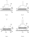
- FIGS 1a-d show schematic sectional views of a substrate adapter 101 known from the prior art Figure 1a is shown includes the substrate adapter 101 a contacting material layer 105 which is arranged between one side of a carrier 109 and a surface of a substrate 103.
- the substrate adapter 101 shown additionally has an adhesive layer 107 which is arranged on the carrier 109 between the carrier 109 and the contacting material layer 105.
- Figure 1a further shows a nozzle 111 for detaching the substrate 103 together with the applied contacting material layer 105 from the carrier 109 in the context of a pickand place process.
- the nozzle 111 is in contact with a surface of the substrate 103 that faces away from the contacting material layer 105.
- the substrate 103 is now detached from the carrier 109 by means of a vacuum, as is shown in FIG Figure 1c is shown.
- the arrow above the nozzle 111 indicates the direction of movement.
- the uncontrolled breaking out generally has a negative impact on the production yield and the product quality of the resulting product, since rejects occur and / or defective parts are further processed.
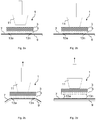
- FIGS. 2a-d show schematic sectional views of a substrate adapter 1 according to an embodiment of the invention.
- the substrate adapter 1 shown comprises a contacting material layer 5, which is arranged between one side of a carrier 9 and a surface of a substrate 3.
- the contacting material layer 5 can comprise an adhesive, a solder and / or a sintered material, in particular a sintering paste and / or a sintered film, which preferably comprises / comprises silver, a silver alloy, copper and / or a copper alloy.
- Substrate 3 can be a metal sheet or a metal strip section, in particular a copper sheet or a copper strip section.
- a copper sheet is also to be understood as a sheet which consists of a copper alloy material.
- a copper band section can be such a band section, which consists of a copper alloy material.
- the substrate 3 can be a lead frame or a DCB substrate or a PCB substrate.
- the carrier 9 can be a carrier film, in particular a carrier film with low adhesive force. Furthermore, it is possible to cover a wafer frame with UV tape in order to produce a carrier 9.
- the substrate 3 provided with the contacting material layer 5 can be glued to this UV tape.
- this adhesive layer 7 is only optional, since the method according to the invention / the substrate adapter 1 according to the invention do not necessarily need such an adhesive layer.
- the Figure 2a further shows a predetermined breaking point in the form of three-dimensional structures 13a-13n, which in the embodiment shown are configured pyramid-shaped. In further embodiments, however, the three-dimensional structures can also be configured pyramid-shaped, spherical, cube-shaped, toroidal, and / or conical.
- the material cutouts are formed from the spaces between adjacent three-dimensional structures 13a-13n. In the embodiment shown, the material cutouts are arranged on the adhesive layer 7 in order to enable a controlled detachment. In embodiments that are not shown, the material recesses can also be arranged at any position in the contacting material layer in order to enable controlled detachment.
- the nozzle 11 is in contact with a surface of the substrate 3 that faces away from the contact material layer 5.
- Figure 2c it is shown that the substrate 3 is detached from the carrier 9 by means of a vacuum.
- the arrow above the nozzle 11 indicates the direction of movement.
- the contacting material layer 5 breaks off along the predetermined breaking point, as shown in FIG Figure 2d is shown. This results in uncontrolled outbreaks within the contacting material layer 5 greatly reduced or prevented when detached from the carrier 9. In this way, the production yield and the product quality of the resulting product can advantageously be increased, since neither rejects arise nor faulty parts are processed further.
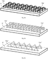
- FIGS. 3a-c show isometric views of three-dimensional structures 13a '- 13n', 13a "- 13n", 13a '"- 13n'" according to embodiments of the invention.
- spherical three-dimensional structures 13a '- 13n' are shown in the contacting material layer 5 '.
- cube-shaped three-dimensional structures 13a "- 13n” are shown in the contacting material layer 5 ".
- pyramid-shaped three-dimensional structures 13a '"- 13n'" are shown in the contacting material layer 5 '".
- three-dimensional structures can be formed in the contacting material layer.
- only two three-dimensional structures can be used to create only one material recess as a predetermined breaking point.
Landscapes
- Engineering & Computer Science (AREA)
- Manufacturing & Machinery (AREA)
- Microelectronics & Electronic Packaging (AREA)
- Electric Connection Of Electric Components To Printed Circuits (AREA)
Abstract
Anordnen zumindest einer Kontaktierungsmaterial-Schicht (5) zwischen zumindest einer Seite eines Trägers (9) und einer Oberfläche eines Substrats (3) derart, dass die Kontaktierungsmaterial-Schicht (5) zumindest eine Sollbruchstelle aufweist; und
Fügen des Trägers (9) und des Substrats (3) mit der Kontaktierungsmaterial-Schicht (5).
Description
- Die vorliegende Erfindung betrifft ein Verfahren zum Herstellen eines Substratadapters. Weiterhin betrifft die vorliegende Erfindung einen Substratadapter zum Verbinden mit einem Elektronikbauteil.
- Substratadapter sind aus dem Stand der Technik bekannt und werden in der Leistungselektronik eingesetzt. Diese Substratadapter sind gewöhnlich als Verbundmaterialen ausgestaltet, die ein Kontaktierungsmaterial in Form einer porösen oder spröden Schicht, beispielsweise eine sinterbare Schicht oder eine Klebstoffschicht umfassen. Diese poröse oder sinterbare Schicht wird, wie es aus dem Stand der Technik bekannt ist, zunächst auf ein Substrat oder einen Träger, beispielsweise einer Trägerfolie aufgebracht und danach werden diese Schichten zu einem Schichtverbund zusammengefügt. In der
DE 10 2011 083 926 A1 wird beispielsweise ein Schichtverbund aus einer Trägerfolie und einer Schichtanordnung umfassend eine poröse oder sinterbare Schicht und eine Lotschicht beschrieben. Die poröse oder sinterbare Schicht kann auf Elektronikbauteile oder elektronische Bauteile angefügt werden, um dadurch verbesserte Verbindungen zwischen verschiedenen Elektronikbauteilen zu ermöglichen. In einem solchen Verfahren wird die Schichtanordnung von der Trägerfolie abgehoben und die poröse oder sinterbare Schicht wird auf das Elektronikbauteil aufgebracht. - Weiterhin beschreibt die
DE 10 2009 018 541 A1 ein Kontaktierungsmittel für Elektronikbauteile mit einer porösen oder sinterbaren Schicht mit gedruckten metallischen Verbindungsstrukturen. - Allerdings haben die aus dem Stand der Technik bekannten Lösungen den Nachteil, dass es beim Ablösen der porösen oder sinterbaren Schichten zu unkontrollierten Ausbrüchen innerhalb der Schichten kommen kann. Außerdem wirkt sich das unkontrollierte Ausbrechen negativ auf die Produktionsausbeute und die Produktqualität des entstehenden Produkts aus, da Ausschuss entsteht oder fehlerhafte Teile weiter prozessiert werden.
- Aufgabe der vorliegenden Erfindung ist es daher, ein verbessertes Verfahren zum Herstellen eines Substratadapters und einen Substratadapter bereitzustellen, das/der die Nachteile des Stands der Technik überwindet. Insbesondere ein Ausbrechen der Kontaktierungsmaterial-Schicht zu verhindern, so dass das Ablösen der Bauteile reproduzierbar und mit einer gleichen Qualität erfolgen kann, um damit eine robusten Bestückungsprozess und eine hohe Produktionsausbeute zu ermöglichen.
- Diese Aufgabe wird erfindungsgemäß durch ein Verfahren zum Herstellen eines Substratadapters gemäß des Gegenstands des Patentanspruchs 1 gelöst.
- Das erfindungsgemäße Verfahren zum Herstellen eines Substratadapters zum Verbinden mit einem Elektronikbauteil weist die folgenden Schritte auf:
Anordnen zumindest einer Kontaktierungsmaterial-Schicht zwischen zumindest einer Seite eines Trägers und einer Oberfläche eines Substrats derart, dass die Kontaktierungsmaterial-Schicht zumindest eine Sollbruchstelle aufweist; und
Fügen des Trägers und des Substrats mit der Kontaktierungsmaterial-Schicht. - Bei dem Substrat kann es sich um ein Metallblech oder um einen Metallbandabschnitt, insbesondere um ein Kupferblech oder um einen Kupferbandabschnitt, handeln. Als Kupferblech ist auch ein Blech zu verstehen, das aus einem Kupferlegierungsmaterial besteht. Bei einem Kupferbandabschnitt kann es sich um einen derartigen Bandabschnitt handeln, der aus einem Kupferlegierungsmaterial besteht. Des Weiteren ist es möglich, dass das Substrat ein Leadframe oder ein DCB-Substrat oder ein PCB-Substrat ist. Vorzugsweise ist das Metallblech oder der Metallbandabschnitt, insbesondere das Kupferblech oder der Kupferbandabschnitt, nicht vorstrukturiert. Lediglich eine Ablängung und/oder Strukturierung der Seitenränder kann bei dem zu verwendenden Substrat durchgeführt worden sein.
- Das Substrat kann auf mindestens einer Seite, insbesondere mit einem Material, das Gold (Au) oder Nickel-Gold (NiAu) oder Silber (Ag) oder Nickel-Silber (NiAg) oder Nickel-Palladium-Gold (NiPdAu) umfasst, beschichtet, insbesondere galvanisiert sein. Außerdem ist es möglich, dass das Material auf mindestens einer Seite des Substrats chemisch abgeschieden wird. Vorzugsweise wird das Substrat, insbesondere mit den genannten Materialien, auf mindestens der Seite beschichtet, die später kontaktiert werden soll. Außerdem ist es denkbar, dass beide Seiten des Substrats beispielsweise mit den vorgenannten Materialien beschichtet werden.
- Die Kontaktierungsmaterial-Schicht, die eine Sinterpaste, insbesondere eine silberhaltige Sinterpaste, oder ein Lot oder ein Leitkleber oder eine Klebefolie sein kann, dient zum tatsächlichen Verbinden des Substrats mit dem Elektronikbauteil.
- Bei dem Träger kann es sich beispielsweise um eine Trägerfolie, insbesondere um eine Trägerfolie mit geringer Adhäsionskraft, handeln. Des Weiteren ist es möglich, zum Herstellen eines Trägers einen Wafer-Frame mit UV-Tape zu bespannen. Das mit einer Schicht des Kontaktierungsmaterials versehene Substrat kann auf dieses UV-Tape geklebt werden. Alternativ hierzu kann die Kontaktierungsmaterial-Schicht auch auf den Träger aufgetragen werden und das Substrat auf der Kontaktierungsmaterial-Schicht angeordnet werden. Der Träger dient dazu, dass der Substratadapter von einer ersten Produktionsstätte zu einer weiteren Produktionsstätte bzw. von einer ersten Fertigungsvorrichtung zu einer weiteren Fertigungsvorrichtung transportiert werden kann.
- Erfindungsgemäß weist die Kontaktierungsmaterial-Schicht zumindest eine Sollbruchstelle auf. Als "Sollbruchstelle" kann in diesem Zusammenhang ein Bereich in der bzw. an der Kontaktierungsmaterial-Schicht verstanden werden, der bei Überlast gezielt und vorhersagbar versagt und hierdurch die Kontaktierungsmaterial-Schicht kontrolliert entlang dieser Sollbruchstelle getrennt wird. Diese Sollbruchstelle kann sich in einer Fläche oder in einem Flächenabschnitt in der Kontaktierungsmaterial-Schicht befinden, die/der sich insbesondere parallel zur Oberfläche des Substrats erstreckt.
- Die Sollbruchstelle kann beispielsweise gebildet sein aus Materialaussparungen in einer Fläche der Kontaktierungsmaterial-Schicht oder dem Einbringen, insbesondere dem flächigen Einbringen von einer, beispielsweise im Physikalischen Gasphasenabscheidungs, PVD, Verfahren hergestellten, Trennschicht in der Kontaktierungsmaterial-Schicht.
- Mit der Erfindung ist es erstmalig gelungen, unkontrollierte Ausbrüche innerhalb der Kontaktierungsmaterial-Schicht beim Ablösen von dem Träger stark zu reduzieren, bzw. zu verhindern. Vorteilhaft kann hierdurch die Produktionsausbeute und die Produktqualität des entstehenden Produkts gesteigert werden, da weder Ausschuss entsteht noch fehlerhafte Teile weiter prozessiert werden.
- In einem Beispiel weist das Anordnen der Kontaktierungsmaterial-Schicht auf:
Anordnen der Kontaktierungsmaterial-Schicht mit mindestens einer Materialaussparung in der Kontaktierungsmaterial-Schicht, vorzugsweise mit einer Vielzahl von Materialaussparungen, um die Sollbruchstelle zu bilden, insbesondere wobei die Materialaussparrungen auf einer Oberfläche der Kontaktierungsmaterial-Schicht angeordnet sind und/oder dem Träger zugewandt sind. - Die Materialaussparungen können durch einen Bereich in der Kontaktierungsmaterial-Schicht gebildet sein, der im Wesentlichen parallel zu dem Substrat verläuft und in dessen flächenmäßigen Verlauf weniger als 50 % Kontaktierungsmaterial angeordnet ist. Weiterhin kann der Bereich mit den Materialaussparungen auf einer dem Träger zugewandten Oberfläche der Kontaktierungsmaterial-Schicht ausgebildet sein, so dass der Träger nicht vollflächig von der Kontaktierungsmaterial-Schicht bedeckt ist.
- In einem Beispiel weist das Anordnen der Kontaktierungsmaterial-Schicht auf:
Anordnen der Kontaktierungsmaterial-Schicht zumindest bereichsweise in Form von dreidimensionalen Strukturen, insbesondere in Form von pyramidenförmigen, kugelförmigen, würfelförmigen, torusförmigen, zylinderförmigen, und/oder kegelförmigen Strukturen, wobei die Materialaussparung, vorzugsweise die Materialaussparungen, aus mindestens einem Zwischenraum zwischen benachbarten dreidimensionalen Strukturen gebildet wird/werden. - Beispielsweise kann ein erster Teil der Kontaktierungsmaterial-Schicht in Form einer im Wesentlichen ebenen Schicht bereitgestellt werden und ein zweiter Teil der Kontaktierungsmaterial-Schicht kann auf dieser Schicht in Form der oben beschriebenen dreidimensionalen Strukturen angeordnet werden.
- In einem Beispiel weist das Anordnen der Kontaktierungsmaterial-Schicht auf:
- Anordnen, insbesondere gleichmäßig beabstandetes Anordnen, der dreidimensionalen Strukturen entlang einer ersten Ausdehnungsachse, vorzugsweise entlang der ersten Ausdehnungsachse und einer zweiten Ausdehnungsachse, insbesondere wobei die erste und
- die zweite Ausdehnungsachse in einem Winkel von im Wesentlichen 90° zueinander angeordnet sind.
- Bevorzugt sind die dreidimensionalen Strukturen gleichmäßig über die Oberfläche der Schicht aus Kontaktierungsmaterial verteilt, um hierdurch ein gleichmäßiges und kontrolliertes Ablösen der Kontaktierungsmaterial-Schicht von dem Träger zu ermöglichen.
- In einem weiteren Beispiel weist das Anordnen der Kontaktierungsmaterial-Schicht auf: Anordnen der Kontaktierungsmaterial-Schicht auf dem Träger durch Drucken, insbesondere durch Siebdrucken, Aufsprühen, und/oder Rakeln, und/oder
Anordnen der Kontaktierungsmaterial-Schicht auf dem Träger durch Verprägen, insbesondere durch Verprägen mittels eines Stempels und/oder einer Profilwalze. - In diesem Beispiel kann eine im Wesentlichen gleichmäßige Schicht des Kontaktierungsmaterials zunächst auf den Träger oder auf das Substrat gedruckt werden und danach dreidimensionale Strukturen, zur Realisierung der Sollbruchstelle, auf die Schicht aufgedruckt werden, oder mittels einer Profilwalze in der Schicht ausgebildet werden.
- Die Kontaktierungsmaterial-Schicht wird vorzugsweise vollflächig, bzw. nahezu vollflächig, auf den Träger oder auf das Substrat aufgebracht. Beispielsweise kann mindestens ein Substrat zum Aufbringen der Kontaktierungsmaterial-Schicht in einem Drucknest positioniert werden. Es ist möglich, dass mehrere Substrate in einem Drucknest positioniert werden. Des Weiteren ist es möglich, dass das Kontaktierungsmaterial zur Bildung einer Kontaktierungsmaterial-Schicht durch ein Sprühverfahren aufgebracht wird. Jedoch ist auch ein Aufbringen mittels eines Rakelverfahrens möglich.
- In einem Beispiel umfasst der Träger zumindest eine Klebeschicht, insbesondere eine Klebeschicht mit einer im Wesentlichen gleichbleibenden Klebekraft über die Oberfläche des Trägers.
- Vorteilhaft können hierdurch die dreidimensionalen Strukturen der Sollbruchstelle besonders zuverlässig mit dem Träger verbunden werden und somit während des Transportes der Anordnung zwischen verschiedenen Produktionsstätten nicht verrutschen. Weiterhin vorteilhaft unterstützt die Klebeschicht ein kontrolliertes Ablösen der Kontaktierungsmaterial-Schicht von dem Träger.
- In noch einem Beispiel umfasst die Kontaktierungsmaterial-Schicht einen Kleber, ein Lot und/oder ein Sintermaterial, insbesondere eine Sinterpaste und/oder eine Sinterfolie, die vorzugsweise Silber, eine Silberlegierung, Kupfer, und/oder einer Kupferlegierung umfasst/umfassen.
- In einem Beispiel weist das Verfahren auf:
Ablösen des Substratadapters, insbesondere mit einer Greif- oder Ansaugvorrichtung, im Wesentlichen entlang der Sollbruchstelle zwischen der Kontaktierungsmaterial-Schicht und dem Träger. - Das Ablösen des Substrats zusammen mit der aufgebrachten Kontaktierungsmaterial-Schicht von dem Träger kann mit Hilfe einer Düse erfolgen. Im Rahmen eines Pick-and-Place-Prozesses kann das Substrat zusammen mit der aufgebrachten Kontaktierungsmaterial-Schicht entlang der Sollbruchstelle von dem Träger gelöst werden und auf dem Elektronikbauteil aufgebracht werden. Dies kann in einem Schritt erfolgen, d.h. nach dem Ablösen vom Träger kann das Substrat sofort auf dem Elektronikbauteil aufgesetzt werden. Des Weiteren ist es möglich, dass das Ablösen vom Träger und das Aufsetzen des Substrats zusammen mit der Kontaktierungsmaterial-Schicht auf dem Elektronikbauteil in zwei separaten Schritten und somit möglicherweise mit zwei unterschiedlichen Düsen durchgeführt wird.
- Bei dem Elektronikbauteil kann es sich um einen Halbleiter oder um ein DCB-Substrat oder um ein PCB-Substrat handeln. Das Verbinden der Substratanordnung mit dem Elektronikbauteil kann beispielsweise mittels Versintern und/oder Verpressen und/oder Verlöten und/oder Verkleben erfolgen. Mit anderen Worten wird die Substratanordnung mit dem Elektronikbauteil versintert und/oder verpresst und/oder verlötet und/oder verklebt. Vorzugsweise wird die Substratanordnung mit dem Elektronikbauteil versintert.
- In einem weiteren Beispiel weist das Verfahren auf:
Vereinzeln des mit der Kontaktierungsmaterial-Schicht zusammengefügten Substrats und des Trägers nach dem Fügen des Trägers und des Substrats mit der Kontaktierungsmaterial-Schicht, insbesondere Unterteilen, vor dem Ablösen des mit der Kontaktierungsmaterial-Schicht zusammengefügten Substrats, in zumindest zwei mit Teilen der Kontaktierungsmaterial-Schicht zusammengefügten Formteile des Substrats, insbesondere in eine Vielzahl von Formteile mittels Sägen, Schneiden, Stanzen und/oder Ätzen. - Nach dem Fügen des Trägers und des Substrats mit der Kontaktierungsmaterial-Schicht kann das Substrat vereinzelt werden.
- Des Weiteren ist es möglich, dass mehrere Substratanordnungen aus einer zunächst größeren Substratanordnung durch Vereinzeln hergestellt werden. Auch ein Strukturieren des Substrats, beispielsweise zur Anpassung des Substrats bzw. der Substratanordnung an die Geometrie des zu verbindenden Bauteils, ist möglich.
- Vorzugsweise erfolgen das Abtrennen des seitlichen Rands und/oder das Strukturieren des Substrats und/oder das Vereinzeln des Substrats mittels Laser. Mit Hilfe eines Laserschneidverfahrens können äußerst kleine Bauteile bearbeitet werden. Des Weiteren können sehr scharfe Kanten mit Hilfe eines Laserschneidverfahrens erzeugt werden.
- Beim Abtrennen des seitlichen Rands und/oder beim Strukturieren des Substrats und/oder beim Vereinzeln des Substrats, insbesondere in einem mit dem Träger verbundenen Zustand des Substrats, kann bzw. können zumindest abschnittsweise die Kontaktierungsmaterial-Schicht abgetrennt und/oder strukturiert und/oder vereinzelt werden.
- In einem Beispiel umfasst das Substrat ein Metallelement, bevorzugt eine Metallfolie, weiter bevorzugt eine Kupferfolie.
- Die Erfindung schlägt auch einen Substratadapter zum Verbinden mit einem Elektronikbauteil vor, aufweisend:
- einen Träger; ein Substrat, und
- eine Kontaktierungsmittel-Schicht, wobei die Kontaktierungsmaterial-Schicht zwischen zumindest einer Seite des Trägers und einer Oberfläche des Substrats angeordnet ist, wobei die Kontaktierungsmaterial-Schicht zumindest eine Sollbruchstelle aufweist, und der Träger und das Substrat mit der Kontaktierungsmaterial-Schicht zusammengefügt sind.
- In einem Beispiel weist die Kontaktierungsmaterial-Schicht mindestens einer Materialaussparung in der Kontaktierungsmaterial-Schicht auf, vorzugsweise eine Vielzahl von Materialaussparungen, um die Sollbruchstelle zu bilden, insbesondere ist die Materialaussparung auf einer Oberfläche der Kontaktierungsmaterial-Schicht angeordnet und/oder dem Träger zugewandt.
- In einem weiteren Beispiel ist die Kontaktierungsmaterial-Schicht zumindest bereichsweise in Form von dreidimensionalen Strukturen angeordnet, insbesondere in Form von pyramidenförmigen, kugelförmigen, würfelförmigen, torusförmigen, zylinderförmigen, und/oder kegelförmigen Strukturen, wobei die Materialaussparung, vorzugsweise die Materialaussparungen, aus mindestens einem Zwischenraum zwischen benachbarten dreidimensionalen Strukturen gebildet wird/werden.
- In einem Beispiel sind die dreidimensionalen Strukturen, insbesondere gleichmäßig beabstandet, entlang einer ersten Ausdehnungsachse, vorzugsweise entlang der ersten Ausdehnungsachse und einer zweiten Ausdehnungsachse angeordnet, insbesondere sind die erste und die zweite Ausdehnungsachse in einem Winkel von im Wesentlichen 90° zueinander angeordnet.
- In noch einem Beispiel umfasst der Träger zumindest eine Klebeschicht, insbesondere eine Klebeschicht mit einer im Wesentlichen gleichbleibenden Klebekraft über die Oberfläche des Trägers, und/oder
die Kontaktierungsmaterial-Schicht umfasst einen Kleber, ein Lot und/oder ein Sintermaterial, insbesondere eine Sinterpaste und/oder eine Sinterfolie, die vorzugsweise Silber, eine Silberlegierung, Kupfer, und/oder einer Kupferlegierung umfasst/umfassen. - Weitere Merkmale und Vorteile der Erfindung ergeben sich aus der nachfolgenden Beschreibung, in der bevorzugte Ausführungsformen der Erfindung anhand von schematischen Zeichnungen erläutert sind.
- Dabei zeigen:
- Figuren 1a-d
- schematische Schnittansichten eines aus dem Stand der Technik bekannten Substratadapters;
- Figuren 2a-d
- schematische Schnittansichten eines Substratadapters gemäß einer Ausführungsform der Erfindung; und
- Figuren 3a-c
- isometrische Ansichten von dreidimensionalen Strukturen gemäß Ausführungsformen der Erfindung.
- Im Folgenden werden für gleiche und gleichwirkende Teile gleiche Bezugsziffern verwendet.
- Die
Figuren 1a-d zeigen schematische Schnittansichten eines aus dem Stand der Technik bekannten Substratadapters 101. Wie es inFigur 1a gezeigt wird, umfasst der Substratadapter 101 eine Kontaktierungsmaterial-Schicht 105, die zwischen einer Seite eines Trägers 109 und einer Oberfläche eines Substrats 103 angeordnet ist. Der in denFiguren 1a-d gezeigte Substratadapter 101 weist zusätzlich eine Klebeschicht 107 auf, die auf dem Träger 109 zwischen dem Träger 109 und der Kontaktierungsmaterial-Schicht 105 angeordnet ist. -
Figur 1a zeigt weiterhin eine Düse 111 zum Ablösen des Substrats 103 zusammen mit der aufgebrachten Kontaktierungsmaterial-Schicht 105 von dem Träger 109 im Rahmen eines Pickand-Place-Prozesses. - In
Figur 1b ist die Düse 111 in Kontakt mit einer Oberfläche des Substrats 103, die der Kontaktierungsmaterial-Schicht 105 abgewandt ist. Mittels eines Vakuums wird nun das Substrat 103 von dem Träger 109 gelöst, wie es in derFigur 1c gezeigt ist. Der Pfeil über der Düse 111 zeigt die Bewegungsrichtung an. Durch das Anheben bzw. Ablösen des Substrats 103 mit der darauf angeordneten Kontaktierungsmaterial-Schicht 105 kann es bei dem aus dem Stand der Technik bekannten Substratadapter 101 bzw. Verfahren dazu führen, dass es beim Ablösen der meist porösen Kontaktierungsmaterial-Schicht 105 zu unkontrollierten Ausbrüchen innerhalb der Kontaktierungsmaterial Schicht 105 kommt. Dies wird inFigur 1c durch eine Bruchlinie 113 in dem Material der Kontaktierungsmaterial-Schicht 105 gezeigt. InFigur 1d ist das von dem Träger 109 abgelöste Substrat 103 mit der ausgebrochenen Kontaktierungsmaterial-Schicht 105 gezeigt. - Das unkontrollierte Ausbrechen wirkt sich im Allgemeinen negativ auf die Produktionsausbeute und die Produktqualität des entstehenden Produkts aus, da Ausschuss entsteht und/oder fehlerhafte Teile weiter prozessiert werden.
- Die
Figuren 2a-d zeigen schematische Schnittansichten eines Substratadapters 1 gemäß einer Ausführungsform der Erfindung. - Auch der in
Figur 2a gezeigte Substratadapter 1 umfasst eine Kontaktierungsmaterial-Schicht 5, die zwischen einer Seite eines Trägers 9 und einer Oberfläche eines Substrats 3 angeordnet ist. - Die Kontaktierungsmaterial-Schicht 5 kann einen Kleber, ein Lot und/oder ein Sintermaterial umfassen, insbesondere eine Sinterpaste und/oder eine Sinterfolie, die vorzugsweise Silber, eine Silberlegierung, Kupfer, und/oder einer Kupferlegierung umfasst/umfassen. Bei dem Substrat 3 kann es sich um ein Metallblech oder um einen Metallbandabschnitt, insbesondere um ein Kupferblech oder um einen Kupferbandabschnitt, handeln. Als Kupferblech ist auch ein Blech zu verstehen, das aus einem Kupferlegierungsmaterial besteht. Bei einem Kupferbandabschnitt kann es sich um einen derartigen Bandabschnitt handeln, der aus einem Kupferlegierungsmaterial besteht. Des Weiteren ist es möglich, dass das Substrat 3 ein Leadframe oder ein DCB-Substrat oder ein PCB-Substrat ist. Bei dem Träger 9 kann es sich um eine Trägerfolie, insbesondere um eine Trägerfolie mit geringer Adhäsionskraft, handeln. Des Weiteren ist es möglich, zum Herstellen eines Trägers 9 einen Wafer-Frame mit UV-Tape zu bespannen. Das mit der Kontaktierungsmaterial-Schicht 5 versehene Substrat 3 kann auf dieses UV-Tape geklebt werden.
- In der gezeigten Ausführungsform ist auf dem Träger 9 eine Klebeschicht 7, insbesondere eine Klebeschicht 7 mit einer im Wesentlichen gleichbleibenden Klebekraft über die Oberfläche des Trägers 9, angeordnet. Diese Klebeschicht 7 ist jedoch nur optional, da das erfindungsgemäße Verfahren/der erfindungsgemäße Substratadapter 1 eine derartige Klebeschicht nicht zwingend benötigen/benötigt.
- Die
Figur 2a zeigt weiterhin eine Sollbruchstelle in Form von dreidimensionalen Strukturen 13a - 13n, die in der gezeigten Ausführungsform pyramidenförmig ausgestaltet sind. In weiteren Ausführungsformen können die dreidimensionalen Strukturen aber auch pyramidenförmig, kugelförmig, würfelförmig, torusförmig, und/oder kegelförmig ausgestaltet sein. Die Materialaussparungen werden aus den Zwischenräumen zwischen benachbarten dreidimensionalen Strukturen 13a - 13n gebildet. In der gezeigten Ausführungsform sind die Materialaussparungen auf der Klebeschicht 7 angeordnet, um hierdurch ein kontrolliertes Ablösen zu ermöglichen. In nicht gezeigten Ausführungsformen können die Materialaussparrungen aber auch an einer beliebigen Position in der Kontaktierungsmaterial-Schicht angeordnet sein, um ein kontrolliertes Ablösen zu ermöglichen. - Wie bereits in
Figur 1b gezeigt, ist auch inFigur 2b die Düse 11 in Kontakt mit einer Oberfläche des Substrats 3, die der Kontaktierungsmaterial-Schicht 5 abgewandt ist. InFigur 2c wird gezeigt, dass mittels eines Vakuums das Substrat 3 von dem Träger 9 gelöst wird. Der Pfeil über der Düse 11 zeigt die Bewegungsrichtung an. Durch das Anheben bzw. Ablösen des Substrats 3 mit der darauf angeordneten Kontaktierungsmaterial-Schicht 5 bricht die Kontaktierungsmaterial-Schicht 5 entlang der Sollbruchstelle ab, wie es inFigur 2d gezeigt ist. Hierdurch werden unkontrollierte Ausbrüche innerhalb der Kontaktierungsmaterial-Schicht 5 beim Ablösen von dem Träger 9 stark reduziert, bzw. verhindert. Vorteilhaft kann hierdurch die Produktionsausbeute und die Produktqualität des entstehenden Produkts gesteigert werden, da weder Ausschuss entsteht noch fehlerhafte Teile weiter prozessiert werden. - Die
Figuren 3a-c zeigen isometrische Ansichten von dreidimensionalen Strukturen 13a' - 13n', 13a" - 13n", 13a'" - 13n'" gemäß Ausführungsformen der Erfindung. - In
Figur 3a werden kugelförmige dreidimensionale Strukturen 13a' - 13n' in der Kontaktierungsmaterial-Schicht 5' gezeigt. InFigur 3b werden würfelförmige dreidimensionale Strukturen 13a" - 13n" in der Kontaktierungsmaterial-Schicht 5" gezeigt. InFigur 3a werden pyramidenförmige dreidimensionale Strukturen 13a'" - 13n'" in der Kontaktierungsmaterial-Schicht 5'" gezeigt. - In alternativen Ausführungsformen können aber auch weitere Formen verwendet werden. Weiterhin können auch mehr oder weniger dreidimensionale Strukturen, als gezeigt, in der Kontaktierungsmaterial-Schicht ausgeformt sein. Beispielsweise können in einer Ausführungsform lediglich zwei dreidimensionale Strukturen verwendet werden, um lediglich eine Materialausnehmung als Sollbruchstelle zu schaffen.
- Die in der vorstehenden Beschreibung, in den Ansprüchen und in den Figuren dargestellten Merkmale können sowohl einzeln als auch in beliebiger Kombination wesentlich für die Erfindung in ihren verschiedenen Ausführungsformen sein.
-
- 1
- Substratadapter
- 3
- Substrat
- 5
- Kontaktierungsmaterial-Schicht
- 7
- Klebeschicht
- 9
- Träger
- 11
- Düse
- 13a-13n - 13a'''-13n'''
- Dreidimensionale Strukturen
-
- 101
- Substratadapter
- 103
- Substrat
- 105
- Kontaktierungsmaterial-Schicht
- 107
- Klebeschicht
- 109
- Träger
- 111
- Düse
- 113
- Bruchlinie
Claims (15)
- Verfahren zum Herstellen eines Substratadapters zum Verbinden mit einem Elektronikbauteil, aufweisend die Schritte:Anordnen zumindest einer Kontaktierungsmaterial-Schicht zwischen zumindest einer Seite eines Trägers und einer Oberfläche eines Substrats derart, dass die Kontaktierungsmaterial-Schicht zumindest eine Sollbruchstelle aufweist; undFügen des Trägers und des Substrats mit der Kontaktierungsmaterial-Schicht.
- Das Verfahren nach Anspruch 1, dadurch gekennzeichnet, dass das Anordnen der Kontaktierungsmaterial-Schicht aufweist:
Anordnen der Kontaktierungsmaterial-Schicht mit mindestens einer Materialaussparung in der Kontaktierungsmaterial-Schicht, vorzugsweise mit einer Vielzahl von Materialaussparungen, um die Sollbruchstelle zu bilden, insbesondere wobei die Materialaussparrungen auf einer Oberfläche der Kontaktierungsmaterial-Schicht angeordnet sind und/oder dem Träger zugewandt sind. - Das Verfahren nach Anspruch 2, dadurch gekennzeichnet, dass das Anordnen der Kontaktierungsmaterial-Schicht aufweist:
Anordnen der Kontaktierungsmaterial-Schicht zumindest bereichsweise in Form von dreidimensionalen Strukturen, insbesondere in Form von pyramidenförmigen, kugelförmigen, würfelförmigen, torusförmigen, zylinderförmigen, und/oder kegelförmigen Strukturen, wobei die Materialaussparung, vorzugsweise die Materialaussparungen, aus mindestens einem Zwischenraum zwischen benachbarten dreidimensionalen Strukturen gebildet wird/werden. - Das Verfahren nach Anspruch 3, dadurch gekennzeichnet, dass das Anordnen der Kontaktierungsmaterial-Schicht aufweist:
Anordnen, insbesondere gleichmäßig beabstandetes Anordnen, der dreidimensionalen Strukturen entlang einer ersten Ausdehnungsachse, vorzugsweise entlang der ersten Ausdehnungsachse und einer zweiten Ausdehnungsachse, insbesondere wobei die erste und die zweite Ausdehnungsachse in einem Winkel von im Wesentlichen 90° zueinander angeordnet sind. - Das Verfahren nach einem der vorangehenden Ansprüche, dadurch gekennzeichnet, dass das Anordnen der Kontaktierungsmaterial-Schicht aufweist:Anordnen der Kontaktierungsmaterial-Schicht auf dem Träger durch Drucken, insbesondere durch Siebdrucken, Aufsprühen, und/oder Rakeln, und/oderAnordnen der Kontaktierungsmaterial-Schicht auf dem Träger durch Verprägen, insbesondere durch Verprägen mittels eines Stempels und/oder einer Profilwalze.
- Das Verfahren nach einem der vorangehenden Ansprüche, dadurch gekennzeichnet, dass
der Träger zumindest eine Klebeschicht, insbesondere eine Klebeschicht mit einer im Wesentlichen gleichbleibenden Klebekraft über die Oberfläche des Trägers umfasst. - Das Verfahren nach einem der vorangehenden Ansprüche, dadurch gekennzeichnet, dass
die Kontaktierungsmaterial-Schicht einen Kleber, ein Lot und/oder ein Sintermaterial umfasst, insbesondere eine Sinterpaste und/oder eine Sinterfolie, die vorzugsweise Silber, eine Silberlegierung, Kupfer, und/oder einer Kupferlegierung umfasst/umfassen. - Das Verfahren nach einem der vorangehenden Ansprüche, dadurch gekennzeichnet, dass das Verfahren aufweist:
Ablösen des Substratadapters, insbesondere mit einer Greif- oder Ansaugvorrichtung, im Wesentlichen entlang der Sollbruchstelle zwischen der Kontaktierungsmaterial-Schicht und dem Träger. - Das Verfahren nach einem der vorangehenden Ansprüche, aufweisend:
Vereinzeln des mit der Kontaktierungsmaterial-Schicht zusammengefügten Substrats und des Trägers nach dem Fügen des Trägers und des Substrats mit der Kontaktierungsmaterial-Schicht, insbesondere Unterteilen, vor dem Ablösen des mit der Kontaktierungsmaterial-Schicht zusammengefügten Substrats, in zumindest zwei mit Teilen der Kontaktierungsmaterial-Schicht zusammengefügte Formteile des Substrats, insbesondere in eine Vielzahl von Formteile mittels Sägen, Schneiden, Stanzen und/oder Ätzen. - Das Verfahren nach einem der vorangehenden Ansprüche, dadurch gekennzeichnet, dass
das Substrat ein Metallelement, bevorzugt eine Metallfolie, weiter bevorzugt eine Kupferfolie umfasst. - Ein Substratadapter zum Verbinden mit einem Elektronikbauteil, aufweisend:einen Träger; ein Substrat, undeine Kontaktierungsmittel-Schicht, wobei die Kontaktierungsmaterial-Schicht zwischen zumindest einer Seite des Trägers und einer Oberfläche des Substrats angeordnet ist, wobei die Kontaktierungsmaterial-Schicht zumindest eine Sollbruchstelle aufweist, und der Träger und das Substrat mit der Kontaktierungsmaterial-Schicht zusammengefügt sind.
- Der Substratadapter nach Anspruch 11, dadurch gekennzeichnet, dass die Kontaktierungsmaterial-Schicht mindestens einer Materialaussparung in der Kontaktierungsmaterial-Schicht aufweist, vorzugsweise eine Vielzahl von Materialaussparungen aufweist, um die Sollbruchstelle zu bilden, insbesondere ist die Materialaussparung auf einer Oberfläche der Kontaktierungsmaterial-Schicht angeordnet und/oder dem Träger zugewandt.
- Der Substratadapter nach Anspruch 11 oder 12, dadurch gekennzeichnet, dass die Kontaktierungsmaterial-Schicht zumindest bereichsweise in Form von dreidimensionalen Strukturen angeordnet ist, insbesondere in Form von pyramidenförmigen, kugelförmigen, würfelförmigen, torusförmigen, zylinderförmigen, und/oder kegelförmigen Strukturen, wobei die Materialaussparung, vorzugsweise die Materialaussparungen, aus mindestens einem Zwischenraum zwischen benachbarten dreidimensionalen Strukturen gebildet wird/werden.
- Der Substratadapter nach Anspruch 13, dadurch gekennzeichnet, dass die dreidimensionalen Strukturen, insbesondere gleichmäßig beabstandet, entlang einer ersten Ausdehnungsachse, vorzugsweise entlang der ersten Ausdehnungsachse und einer zweiten Ausdehnungsachse angeordnet sind, insbesondere wobei die erste und die zweite Ausdehnungsachse in einem Winkel von im Wesentlichen 90° zueinander angeordnet sind.
- Der Substratadapter nach einem der Ansprüche 11 bis 14, dadurch gekennzeichnet, dass
der Träger zumindest eine Klebeschicht, insbesondere eine Klebeschicht mit einer im Wesentlichen gleichbleibenden Klebekraft über die Oberfläche des Trägers umfasst, und/oder
die Kontaktierungsmaterial-Schicht einen Kleber, ein Lot und/oder ein Sintermaterial umfasst, insbesondere eine Sinterpaste und/oder eine Sinterfolie, die vorzugsweise Silber, eine Silberlegierung, Kupfer, und/oder einer Kupferlegierung umfasst/umfassen.
Applications Claiming Priority (1)
| Application Number | Priority Date | Filing Date | Title |
|---|---|---|---|
| DE102018221148.5A DE102018221148A1 (de) | 2018-12-06 | 2018-12-06 | Verfahren zum Herstellen eines Substratadapters und Substratadapter zum Verbinden mit einem Elektronikbauteil |
Publications (1)
| Publication Number | Publication Date |
|---|---|
| EP3675153A1 true EP3675153A1 (de) | 2020-07-01 |
Family
ID=67956467
Family Applications (1)
| Application Number | Title | Priority Date | Filing Date |
|---|---|---|---|
| EP19196401.4A Pending EP3675153A1 (de) | 2018-12-06 | 2019-09-10 | Verfahren zum herstellen eines substratadapters und substratadapter zum verbinden mit einem elektronikbauteil |
Country Status (6)
| Country | Link |
|---|---|
| US (1) | US11440310B2 (de) |
| EP (1) | EP3675153A1 (de) |
| JP (1) | JP7036784B2 (de) |
| KR (1) | KR102321949B1 (de) |
| CN (1) | CN111293042B (de) |
| DE (1) | DE102018221148A1 (de) |
Families Citing this family (1)
| Publication number | Priority date | Publication date | Assignee | Title |
|---|---|---|---|---|
| TWI781885B (zh) * | 2022-02-14 | 2022-10-21 | 大陸商芯愛科技(南京)有限公司 | 半導體封裝件之製法及其所用之載板與製法 |
Citations (4)
| Publication number | Priority date | Publication date | Assignee | Title |
|---|---|---|---|---|
| US20070013067A1 (en) * | 1999-01-29 | 2007-01-18 | Kazuto Nishida | Electronic component mounting method and apparatus |
| EP2144283A1 (de) * | 2008-02-05 | 2010-01-13 | Sony Chemical & Information Device Corporation | Verfahren zur übertragung einer haftfolie |
| DE102009018541A1 (de) | 2009-04-24 | 2010-10-28 | W.C. Heraeus Gmbh | Kontaktierungsmittel und Verfahren zur Kontaktierung elektrischer Bauteile |
| DE102011083926A1 (de) | 2011-09-30 | 2013-04-04 | Robert Bosch Gmbh | Schichtverbund aus einer Trägerfolie und einer Schichtanordnung umfassend eine sinterbare Schicht aus mindestens einem Metallpulver und eine Lotschicht |
Family Cites Families (6)
| Publication number | Priority date | Publication date | Assignee | Title |
|---|---|---|---|---|
| JP5066935B2 (ja) | 2007-02-22 | 2012-11-07 | 富士通株式会社 | 電子部品および電子装置の製造方法 |
| JP5196838B2 (ja) * | 2007-04-17 | 2013-05-15 | リンテック株式会社 | 接着剤付きチップの製造方法 |
| DE102012201935A1 (de) * | 2012-02-09 | 2013-08-14 | Robert Bosch Gmbh | Verbindungsanordnung eines elektrischen und/oder elektronischen Bauelements |
| US9196520B1 (en) * | 2014-08-01 | 2015-11-24 | Freescale Semiconductor, Inc. | Tape release systems and methods for semiconductor dies |
| DE102015107724B4 (de) * | 2015-04-02 | 2016-12-01 | Heraeus Deutschland GmbH & Co. KG | Verfahren zum Herstellen einer Substratanordnung, Substratanordnung, Verfahren zum Verbinden eines Elektronikbauteils mit einer Substratanordnung und Elektronikbauteil |
| EP3154079A1 (de) | 2015-10-08 | 2017-04-12 | Heraeus Deutschland GmbH & Co. KG | Verfahren zum verbinden einer substratanordnung mit einem elektronikbauteil mit verwendung eines auf eine kontaktierungsmaterialschicht aufgebrachten vorfixiermittels, entsprechende substratanordnung und verfahren zu ihrem herstellen |
-
2018
- 2018-12-06 DE DE102018221148.5A patent/DE102018221148A1/de active Pending
-
2019
- 2019-09-10 EP EP19196401.4A patent/EP3675153A1/de active Pending
- 2019-10-18 JP JP2019191020A patent/JP7036784B2/ja active Active
- 2019-11-07 CN CN201911083771.0A patent/CN111293042B/zh active Active
- 2019-11-15 KR KR1020190147136A patent/KR102321949B1/ko active Active
- 2019-12-05 US US16/704,145 patent/US11440310B2/en active Active
Patent Citations (4)
| Publication number | Priority date | Publication date | Assignee | Title |
|---|---|---|---|---|
| US20070013067A1 (en) * | 1999-01-29 | 2007-01-18 | Kazuto Nishida | Electronic component mounting method and apparatus |
| EP2144283A1 (de) * | 2008-02-05 | 2010-01-13 | Sony Chemical & Information Device Corporation | Verfahren zur übertragung einer haftfolie |
| DE102009018541A1 (de) | 2009-04-24 | 2010-10-28 | W.C. Heraeus Gmbh | Kontaktierungsmittel und Verfahren zur Kontaktierung elektrischer Bauteile |
| DE102011083926A1 (de) | 2011-09-30 | 2013-04-04 | Robert Bosch Gmbh | Schichtverbund aus einer Trägerfolie und einer Schichtanordnung umfassend eine sinterbare Schicht aus mindestens einem Metallpulver und eine Lotschicht |
Also Published As
| Publication number | Publication date |
|---|---|
| CN111293042B (zh) | 2023-11-28 |
| KR20200070098A (ko) | 2020-06-17 |
| JP2020092257A (ja) | 2020-06-11 |
| US20200180294A1 (en) | 2020-06-11 |
| KR102321949B1 (ko) | 2021-11-04 |
| DE102018221148A1 (de) | 2020-06-10 |
| CN111293042A (zh) | 2020-06-16 |
| US11440310B2 (en) | 2022-09-13 |
| JP7036784B2 (ja) | 2022-03-15 |
Similar Documents
| Publication | Publication Date | Title |
|---|---|---|
| EP3940758A2 (de) | Verfahren zum sinterverbinden einer substratanordnung mit einem elektronikbauteil mit verwendung eines auf eine sinterkontaktierungsmaterialschicht aufgebrachten vorfixiermittels, entsprechende substratanordnung und verfahren zu ihrer herstellung | |
| DE4010370C2 (de) | Verfahren zum Herstellen von Halbleiterbauteilen | |
| EP0140126A1 (de) | Verfahren zur Mikropackherstellung | |
| WO2001071799A2 (de) | Halbleiterbauelement und verfahren zu dessen herstellung | |
| DE102015107724B4 (de) | Verfahren zum Herstellen einer Substratanordnung, Substratanordnung, Verfahren zum Verbinden eines Elektronikbauteils mit einer Substratanordnung und Elektronikbauteil | |
| EP2390904A2 (de) | Verfahren zur Niedertemperatur Drucksinterverbindung zweier Verbindungspartner und hiermit hergestellte Anordnung | |
| DE102014201635B3 (de) | Verfahren zur Anordnung von elektronischen Bauelementen und elektronische Schaltanordnung | |
| EP3026702B1 (de) | Verfahren zum herstellen eines halbleiterelements mit substratadapter und halbleiterelement mit substratadapter | |
| DE19522338B4 (de) | Chipträgeranordnung mit einer Durchkontaktierung | |
| DE102014109766B3 (de) | Verfahren zum Herstellen eines Substratadapters, Substratadapter und Verfahren zum Kontaktieren eines Halbleiterelements | |
| DE102018221148A1 (de) | Verfahren zum Herstellen eines Substratadapters und Substratadapter zum Verbinden mit einem Elektronikbauteil | |
| EP3850924A1 (de) | Verfahren zur herstellung einer leiterplattenanordnung und leiterplattenanordnung | |
| DE3446647C2 (de) | ||
| DE10007414B4 (de) | Verfahren zur Durchkontaktierung eines Substrats für Leistungshalbleitermodule durch Lot und mit dem Verfahren hergestelltes Substrat | |
| WO2005027200A2 (de) | Verfahren und vorrichtung zum kontaktieren von halbleiterchips auf einem metallischen substrat | |
| DE60130108T2 (de) | Verfahren zur herstellung elektrischer verbindungselemente und verbindungselement | |
| DE19946497C2 (de) | Verfahren zur Herstellung einer Verbindung zweier Gegenstände | |
| DE102005016930A1 (de) | Verfahren zum elektrischen und mechanischem Verbinden von Chipanschlussflächen mit Antennenanschlussflächen und Transponder | |
| EP1298723A2 (de) | Elektronisches Bauteil mit einem Kunststoffgehäuse und Komponenten eines Systemträgers und Verfahren zu deren Herstellung | |
| DE102019111437B4 (de) | Verfahren zur Herstellung eines elektronischen Zwischenprodukts und Verfahren zur Herstellung eines Elektronik-Bauteils | |
| DE10157205A1 (de) | Kontakthöcker mit profilierter Oberflächenstruktur sowie Verfahren zur Herstellung | |
| EP3611761A1 (de) | Verfahren und metallsubstrat zum kontaktieren eines leistungshalbleiters durch ein kontaktierungsmittel mit zumindest einem kontaktierungsfreien bereich als belastungsreduzierende struktur | |
| EP1389407B1 (de) | Verfahren zur herstellung eines kontaktsubstrats sowie kontaktsubstrat | |
| DE102018105861B3 (de) | Verfahren zur Herstellung eines Leiterbahnabschnitts eines Anschlussträgers, Verfahren zur Herstellung eines Anschlussträgers, und optoelektronisches Halbleiterbauteil | |
| EP2539099A1 (de) | Verfahren zum aufbringen von weichlot auf eine montagefläche eines bauelementes |
Legal Events
| Date | Code | Title | Description |
|---|---|---|---|
| PUAI | Public reference made under article 153(3) epc to a published international application that has entered the european phase |
Free format text: ORIGINAL CODE: 0009012 |
|
| STAA | Information on the status of an ep patent application or granted ep patent |
Free format text: STATUS: REQUEST FOR EXAMINATION WAS MADE |
|
| 17P | Request for examination filed |
Effective date: 20190910 |
|
| AK | Designated contracting states |
Kind code of ref document: A1 Designated state(s): AL AT BE BG CH CY CZ DE DK EE ES FI FR GB GR HR HU IE IS IT LI LT LU LV MC MK MT NL NO PL PT RO RS SE SI SK SM TR |
|
| AX | Request for extension of the european patent |
Extension state: BA ME |
|
| RAP3 | Party data changed (applicant data changed or rights of an application transferred) |
Owner name: HERAEUS DEUTSCHLAND GMBH & CO. KG |
|
| RAP1 | Party data changed (applicant data changed or rights of an application transferred) |
Owner name: HERAEUS ELECTRONICS GMBH & CO. KG |
|
| STAA | Information on the status of an ep patent application or granted ep patent |
Free format text: STATUS: EXAMINATION IS IN PROGRESS |
|
| 17Q | First examination report despatched |
Effective date: 20240119 |