EP3674789B1 - Anzeigevorrichtung - Google Patents
Anzeigevorrichtung Download PDFInfo
- Publication number
- EP3674789B1 EP3674789B1 EP19217832.5A EP19217832A EP3674789B1 EP 3674789 B1 EP3674789 B1 EP 3674789B1 EP 19217832 A EP19217832 A EP 19217832A EP 3674789 B1 EP3674789 B1 EP 3674789B1
- Authority
- EP
- European Patent Office
- Prior art keywords
- line
- pixel
- touch
- sub
- disposed
- Prior art date
- Legal status (The legal status is an assumption and is not a legal conclusion. Google has not performed a legal analysis and makes no representation as to the accuracy of the status listed.)
- Active
Links
Images




Classifications
-
- G—PHYSICS
- G02—OPTICS
- G02F—OPTICAL DEVICES OR ARRANGEMENTS FOR THE CONTROL OF LIGHT BY MODIFICATION OF THE OPTICAL PROPERTIES OF THE MEDIA OF THE ELEMENTS INVOLVED THEREIN; NON-LINEAR OPTICS; FREQUENCY-CHANGING OF LIGHT; OPTICAL LOGIC ELEMENTS; OPTICAL ANALOGUE/DIGITAL CONVERTERS
- G02F1/00—Devices or arrangements for the control of the intensity, colour, phase, polarisation or direction of light arriving from an independent light source, e.g. switching, gating or modulating; Non-linear optics
- G02F1/01—Devices or arrangements for the control of the intensity, colour, phase, polarisation or direction of light arriving from an independent light source, e.g. switching, gating or modulating; Non-linear optics for the control of the intensity, phase, polarisation or colour
- G02F1/13—Devices or arrangements for the control of the intensity, colour, phase, polarisation or direction of light arriving from an independent light source, e.g. switching, gating or modulating; Non-linear optics for the control of the intensity, phase, polarisation or colour based on liquid crystals, e.g. single liquid crystal display cells
- G02F1/133—Constructional arrangements; Operation of liquid crystal cells; Circuit arrangements
- G02F1/1333—Constructional arrangements; Manufacturing methods
- G02F1/13338—Input devices, e.g. touch panels
-
- G—PHYSICS
- G02—OPTICS
- G02F—OPTICAL DEVICES OR ARRANGEMENTS FOR THE CONTROL OF LIGHT BY MODIFICATION OF THE OPTICAL PROPERTIES OF THE MEDIA OF THE ELEMENTS INVOLVED THEREIN; NON-LINEAR OPTICS; FREQUENCY-CHANGING OF LIGHT; OPTICAL LOGIC ELEMENTS; OPTICAL ANALOGUE/DIGITAL CONVERTERS
- G02F1/00—Devices or arrangements for the control of the intensity, colour, phase, polarisation or direction of light arriving from an independent light source, e.g. switching, gating or modulating; Non-linear optics
- G02F1/01—Devices or arrangements for the control of the intensity, colour, phase, polarisation or direction of light arriving from an independent light source, e.g. switching, gating or modulating; Non-linear optics for the control of the intensity, phase, polarisation or colour
- G02F1/13—Devices or arrangements for the control of the intensity, colour, phase, polarisation or direction of light arriving from an independent light source, e.g. switching, gating or modulating; Non-linear optics for the control of the intensity, phase, polarisation or colour based on liquid crystals, e.g. single liquid crystal display cells
- G02F1/133—Constructional arrangements; Operation of liquid crystal cells; Circuit arrangements
- G02F1/1333—Constructional arrangements; Manufacturing methods
- G02F1/1343—Electrodes
- G02F1/134309—Electrodes characterised by their geometrical arrangement
- G02F1/134363—Electrodes characterised by their geometrical arrangement for applying an electric field parallel to the substrate, i.e. in-plane switching [IPS]
-
- G—PHYSICS
- G02—OPTICS
- G02F—OPTICAL DEVICES OR ARRANGEMENTS FOR THE CONTROL OF LIGHT BY MODIFICATION OF THE OPTICAL PROPERTIES OF THE MEDIA OF THE ELEMENTS INVOLVED THEREIN; NON-LINEAR OPTICS; FREQUENCY-CHANGING OF LIGHT; OPTICAL LOGIC ELEMENTS; OPTICAL ANALOGUE/DIGITAL CONVERTERS
- G02F1/00—Devices or arrangements for the control of the intensity, colour, phase, polarisation or direction of light arriving from an independent light source, e.g. switching, gating or modulating; Non-linear optics
- G02F1/01—Devices or arrangements for the control of the intensity, colour, phase, polarisation or direction of light arriving from an independent light source, e.g. switching, gating or modulating; Non-linear optics for the control of the intensity, phase, polarisation or colour
- G02F1/13—Devices or arrangements for the control of the intensity, colour, phase, polarisation or direction of light arriving from an independent light source, e.g. switching, gating or modulating; Non-linear optics for the control of the intensity, phase, polarisation or colour based on liquid crystals, e.g. single liquid crystal display cells
- G02F1/133—Constructional arrangements; Operation of liquid crystal cells; Circuit arrangements
- G02F1/136—Liquid crystal cells structurally associated with a semi-conducting layer or substrate, e.g. cells forming part of an integrated circuit
- G02F1/1362—Active matrix addressed cells
- G02F1/136204—Arrangements to prevent high voltage or static electricity failures
-
- G—PHYSICS
- G02—OPTICS
- G02F—OPTICAL DEVICES OR ARRANGEMENTS FOR THE CONTROL OF LIGHT BY MODIFICATION OF THE OPTICAL PROPERTIES OF THE MEDIA OF THE ELEMENTS INVOLVED THEREIN; NON-LINEAR OPTICS; FREQUENCY-CHANGING OF LIGHT; OPTICAL LOGIC ELEMENTS; OPTICAL ANALOGUE/DIGITAL CONVERTERS
- G02F1/00—Devices or arrangements for the control of the intensity, colour, phase, polarisation or direction of light arriving from an independent light source, e.g. switching, gating or modulating; Non-linear optics
- G02F1/01—Devices or arrangements for the control of the intensity, colour, phase, polarisation or direction of light arriving from an independent light source, e.g. switching, gating or modulating; Non-linear optics for the control of the intensity, phase, polarisation or colour
- G02F1/13—Devices or arrangements for the control of the intensity, colour, phase, polarisation or direction of light arriving from an independent light source, e.g. switching, gating or modulating; Non-linear optics for the control of the intensity, phase, polarisation or colour based on liquid crystals, e.g. single liquid crystal display cells
- G02F1/133—Constructional arrangements; Operation of liquid crystal cells; Circuit arrangements
- G02F1/136—Liquid crystal cells structurally associated with a semi-conducting layer or substrate, e.g. cells forming part of an integrated circuit
- G02F1/1362—Active matrix addressed cells
- G02F1/136259—Repairing; Defects
-
- G—PHYSICS
- G02—OPTICS
- G02F—OPTICAL DEVICES OR ARRANGEMENTS FOR THE CONTROL OF LIGHT BY MODIFICATION OF THE OPTICAL PROPERTIES OF THE MEDIA OF THE ELEMENTS INVOLVED THEREIN; NON-LINEAR OPTICS; FREQUENCY-CHANGING OF LIGHT; OPTICAL LOGIC ELEMENTS; OPTICAL ANALOGUE/DIGITAL CONVERTERS
- G02F1/00—Devices or arrangements for the control of the intensity, colour, phase, polarisation or direction of light arriving from an independent light source, e.g. switching, gating or modulating; Non-linear optics
- G02F1/01—Devices or arrangements for the control of the intensity, colour, phase, polarisation or direction of light arriving from an independent light source, e.g. switching, gating or modulating; Non-linear optics for the control of the intensity, phase, polarisation or colour
- G02F1/13—Devices or arrangements for the control of the intensity, colour, phase, polarisation or direction of light arriving from an independent light source, e.g. switching, gating or modulating; Non-linear optics for the control of the intensity, phase, polarisation or colour based on liquid crystals, e.g. single liquid crystal display cells
- G02F1/133—Constructional arrangements; Operation of liquid crystal cells; Circuit arrangements
- G02F1/136—Liquid crystal cells structurally associated with a semi-conducting layer or substrate, e.g. cells forming part of an integrated circuit
- G02F1/1362—Active matrix addressed cells
- G02F1/136259—Repairing; Defects
- G02F1/136263—Line defects
-
- G—PHYSICS
- G02—OPTICS
- G02F—OPTICAL DEVICES OR ARRANGEMENTS FOR THE CONTROL OF LIGHT BY MODIFICATION OF THE OPTICAL PROPERTIES OF THE MEDIA OF THE ELEMENTS INVOLVED THEREIN; NON-LINEAR OPTICS; FREQUENCY-CHANGING OF LIGHT; OPTICAL LOGIC ELEMENTS; OPTICAL ANALOGUE/DIGITAL CONVERTERS
- G02F1/00—Devices or arrangements for the control of the intensity, colour, phase, polarisation or direction of light arriving from an independent light source, e.g. switching, gating or modulating; Non-linear optics
- G02F1/01—Devices or arrangements for the control of the intensity, colour, phase, polarisation or direction of light arriving from an independent light source, e.g. switching, gating or modulating; Non-linear optics for the control of the intensity, phase, polarisation or colour
- G02F1/13—Devices or arrangements for the control of the intensity, colour, phase, polarisation or direction of light arriving from an independent light source, e.g. switching, gating or modulating; Non-linear optics for the control of the intensity, phase, polarisation or colour based on liquid crystals, e.g. single liquid crystal display cells
- G02F1/133—Constructional arrangements; Operation of liquid crystal cells; Circuit arrangements
- G02F1/136—Liquid crystal cells structurally associated with a semi-conducting layer or substrate, e.g. cells forming part of an integrated circuit
- G02F1/1362—Active matrix addressed cells
- G02F1/136286—Wiring, e.g. gate line, drain line
-
- G—PHYSICS
- G02—OPTICS
- G02F—OPTICAL DEVICES OR ARRANGEMENTS FOR THE CONTROL OF LIGHT BY MODIFICATION OF THE OPTICAL PROPERTIES OF THE MEDIA OF THE ELEMENTS INVOLVED THEREIN; NON-LINEAR OPTICS; FREQUENCY-CHANGING OF LIGHT; OPTICAL LOGIC ELEMENTS; OPTICAL ANALOGUE/DIGITAL CONVERTERS
- G02F1/00—Devices or arrangements for the control of the intensity, colour, phase, polarisation or direction of light arriving from an independent light source, e.g. switching, gating or modulating; Non-linear optics
- G02F1/01—Devices or arrangements for the control of the intensity, colour, phase, polarisation or direction of light arriving from an independent light source, e.g. switching, gating or modulating; Non-linear optics for the control of the intensity, phase, polarisation or colour
- G02F1/13—Devices or arrangements for the control of the intensity, colour, phase, polarisation or direction of light arriving from an independent light source, e.g. switching, gating or modulating; Non-linear optics for the control of the intensity, phase, polarisation or colour based on liquid crystals, e.g. single liquid crystal display cells
- G02F1/133—Constructional arrangements; Operation of liquid crystal cells; Circuit arrangements
- G02F1/136—Liquid crystal cells structurally associated with a semi-conducting layer or substrate, e.g. cells forming part of an integrated circuit
- G02F1/1362—Active matrix addressed cells
- G02F1/1368—Active matrix addressed cells in which the switching element is a three-electrode device
-
- G—PHYSICS
- G02—OPTICS
- G02F—OPTICAL DEVICES OR ARRANGEMENTS FOR THE CONTROL OF LIGHT BY MODIFICATION OF THE OPTICAL PROPERTIES OF THE MEDIA OF THE ELEMENTS INVOLVED THEREIN; NON-LINEAR OPTICS; FREQUENCY-CHANGING OF LIGHT; OPTICAL LOGIC ELEMENTS; OPTICAL ANALOGUE/DIGITAL CONVERTERS
- G02F1/00—Devices or arrangements for the control of the intensity, colour, phase, polarisation or direction of light arriving from an independent light source, e.g. switching, gating or modulating; Non-linear optics
- G02F1/01—Devices or arrangements for the control of the intensity, colour, phase, polarisation or direction of light arriving from an independent light source, e.g. switching, gating or modulating; Non-linear optics for the control of the intensity, phase, polarisation or colour
- G02F1/13—Devices or arrangements for the control of the intensity, colour, phase, polarisation or direction of light arriving from an independent light source, e.g. switching, gating or modulating; Non-linear optics for the control of the intensity, phase, polarisation or colour based on liquid crystals, e.g. single liquid crystal display cells
- G02F1/133—Constructional arrangements; Operation of liquid crystal cells; Circuit arrangements
- G02F1/136—Liquid crystal cells structurally associated with a semi-conducting layer or substrate, e.g. cells forming part of an integrated circuit
- G02F1/1362—Active matrix addressed cells
- G02F1/136286—Wiring, e.g. gate line, drain line
- G02F1/13629—Multilayer wirings
-
- G—PHYSICS
- G02—OPTICS
- G02F—OPTICAL DEVICES OR ARRANGEMENTS FOR THE CONTROL OF LIGHT BY MODIFICATION OF THE OPTICAL PROPERTIES OF THE MEDIA OF THE ELEMENTS INVOLVED THEREIN; NON-LINEAR OPTICS; FREQUENCY-CHANGING OF LIGHT; OPTICAL LOGIC ELEMENTS; OPTICAL ANALOGUE/DIGITAL CONVERTERS
- G02F2201/00—Constructional arrangements not provided for in groups G02F1/00 - G02F7/00
- G02F2201/12—Constructional arrangements not provided for in groups G02F1/00 - G02F7/00 electrode
- G02F2201/121—Constructional arrangements not provided for in groups G02F1/00 - G02F7/00 electrode common or background
-
- G—PHYSICS
- G02—OPTICS
- G02F—OPTICAL DEVICES OR ARRANGEMENTS FOR THE CONTROL OF LIGHT BY MODIFICATION OF THE OPTICAL PROPERTIES OF THE MEDIA OF THE ELEMENTS INVOLVED THEREIN; NON-LINEAR OPTICS; FREQUENCY-CHANGING OF LIGHT; OPTICAL LOGIC ELEMENTS; OPTICAL ANALOGUE/DIGITAL CONVERTERS
- G02F2201/00—Constructional arrangements not provided for in groups G02F1/00 - G02F7/00
- G02F2201/12—Constructional arrangements not provided for in groups G02F1/00 - G02F7/00 electrode
- G02F2201/123—Constructional arrangements not provided for in groups G02F1/00 - G02F7/00 electrode pixel
Definitions
- the present invention relates to a display device capable of preventing a touch sensing error.
- An LCD images by controlling electric fields applied to liquid crystal molecules according to a data voltage.
- An active matrix type LCD includes a thin film transistor (TFT) formed at each pixel. Pixels of the LCD may be divided into R sub-pixels, G sub-pixels, B sub-pixels and W sub-pixels to represent colors and improve luminance.
- TFT thin film transistor
- An LCD includes a liquid crystal display panel, a back light unit for radiating light to the liquid crystal display panel, a source drive integrated circuit (IC) for providing data voltages to data lines of the liquid crystal display panel, a gate drive IC for providing gate pulses (or scan pulses) to gate lines (or scan lines) of the liquid crystal display panel, a control circuit for controlling the ICs, a light source driver for driving a light source of the back light unit, and the like.
- IC integrated circuit
- Prior art display devices are disclosed in EP3316103 A1 , which concerns repairing of touch electrode lines, in US2017269446 A1 , which concerns repairing of a defective data line by means of a repair line and two adjacent touch electrode lines, as well as in US2008225196 A1 and in US6985194 B2 , which both concern repairing of pixels by laser welding a pixel electrode to the gate line in order to darken a bright pixel. None of those prior art documents disclose a repair region in an area in which the pixel electrode and the touch routing line overlap, and a common electrode connector does not overlap with the repair portion.
- LCD is driven in an inversion mode in which data voltages having opposite polarities are charged in neighboring sub-pixels and the data voltage polarities are periodically inverted in order to reduce DC afterimage and prevent liquid crystal deterioration.
- Horizontal and vertical 1-dot inversion or horizontal 1-dot and vertical 2-dot inversion is applied to most LCD devices. 1 dot refers to 1 sub-pixel.
- DRD double rating driving
- a sub-pixel structure for DRD has a complicated design because channels and pixel electrodes are arranged zigzag.
- the present invention provides a display device which includes a self-capacitance type touch sensor and sub-pixels for DRD and can prevent a touch sensing error during a sub-pixel repair process.
- the touch type display device includes a substrate, a first data line disposed on the substrate, a touch routing line which may be disposed in parallel with the first data line, a first gate line which intersects the first data line and the touch routing line, and a first sub-pixel defined according to intersections of the first data line and the touch routing line with the first gate line.
- the first sub-pixel includes a thin film transistor disposed at the intersection of the first data line and the first gate line.
- the first sub-pixel further includes a pixel electrode connected to the thin film transistor and a common electrode overlapped on the pixel electrode.
- the common electrode includes a common electrode connector extending to a second sub-pixel neighboring the first sub-pixel.
- the touch routing line and the common electrode connector are disposed to overlap with each other.
- a repair portion where laser welding can be performed, is included in an area in which the pixel electrode and the touch routing line overlap.
- the common electrode connector does not overlap with the repair portion.
- the common electrode connector may include a center part and line parts respectively extended to one side and the other side from the center part.
- the center part has a first width
- the line parts have a second width
- the first width may be greater than the second width
- the line parts may be disposed on different sides on the basis of a center line of the center part.
- the line parts may be disposed on both sides of the central part along the central line.
- the touch routing line may include a center part, extended parts respectively extended to one side and the other side from the center part, and line parts respectively extended from the extended parts.
- the center part has a third width
- the extended parts have a fifth width
- the line parts have a fourth width
- the third width may be greater than each of the fourth width and the fifth width.
- the fifth width is greater than the fourth width.
- each extended part may be formed such that a first part i.e. a left-hand side part and a second part i.e. a right-hand side part of each extended part with respect to the central line is asymmetrical, for example a width of the left-hand side part and a width of the right-hand side part of each extended part may be different from each other.
- the common electrode connector and the touch routing line may be formed i.e. shaped and mutually arranged in the display device such that line parts of the common electrode connector and the line parts of the touch routing line do not overlap with each other.
- the center part of the common electrode connector and the center part of the touch routing line may overlap with each other.
- the touch routing line may be electrically short-circuited with respect to the common electrode.
- first and second are used to describe various components, but such components are not limited by these terms. The terms are used to discriminate one component from another component. Accordingly, a first component mentioned in the following description may be a second component within the technical concept of the disclosure.
- FIG. 1 is a block diagram of an LCD
- FIG. 2 is a diagram showing DRD of the LCD
- FIG. 3 is a diagram showing charging voltage waveforms in each liquid crystal cell when liquid crystal cells are charged in the direction of an arrow.
- a display device may be implemented as a flat panel display such as a liquid crystal display (LCD), a field emission display (FED), a plasma display panel (PDP), an organic light emitting diode (OLED) display, or an electrophoresis display (EPD) or the like.
- LCD liquid crystal display
- FED field emission display
- PDP plasma display panel
- OLED organic light emitting diode
- EPD electrophoresis display
- An LCD panel 10 includes a liquid crystal layer formed between two glass substrates.
- the LCD panel 10 includes liquid crystal cells Cls arranged in a matrix form according to an intersection structure of data lines 15 and gate lines 16.
- a pixel array is formed on a lower substrate of the LCD panel 10.
- the pixel array includes liquid crystal cells (pixels) Cls formed at intersections of the data lines 15 and the gate lines 16, thin film transistors (TFTs) connected to pixel electrodes 1 of the pixels, common electrodes 2 opposite the pixel electrodes 1, and storage capacitors Cst.
- Each liquid crystal cell Clc is connected to a switching transistor TFT and driven by electric fields between the pixel electrode 1 and the common electrode 2.
- a black matrix, red (R), green (G) and blue (B) color filters, and the like are formed on an upper substrate of the LCD panel 10.
- a polarizer is attached to each of the upper substrate and the lower substrate and an alignment film for setting a pre-tilt angle of liquid crystal is formed thereon.
- the common electrodes 2 are formed on the lower substrate along with the pixel electrodes 1 in horizontal field driving modes such as an in-plane switching (IPS) mode and a fringe field switching (FFS) mode.
- IPS in-plane switching
- the LCD panel 10 applicable to the present invention can be realized in any liquid crystal mode as well as the IPS mode and the FFS mode.
- the LCD of the present invention can be implemented as any type such as a transmissive LCD, a transflective LCD and a reflective LCD.
- the transmissive LCD and the transflective LCD require a back light unit.
- the back light unit may be implemented as a direct type back light unit or an edge type back light unit.
- the display device of the present invention includes a driver 17 for driving the LCD panel 10.
- the driver 17 changes operation modes according to whether image data RGB input from an external system is a moving image or a still image. For example, the driver 17 operates in a high-speed operation mode having a high driving frequency when the image data RGB is a moving image and operates in a low-speed operation mode having a low driving frequency when the image data RGB is a still image.
- the driver 17 includes a host system 14, a timing controller 11, a source driver 12 and a data driver 13.
- the host system 14 receives image data RGB from an external system, generates an operation mode signal MS corresponding to the image data RGB and outputs the operation mode signal MS to the timing controller 11. Specifically, the host system 14 generates an operation mode signal MS corresponding to a moving image when the image data RGB is the moving image and generate an operation mode signal MS corresponding to a still image when the image data TGB is the still image.
- the operation mode signal MS is a signal for a high-speed mode operation when the image data RGB corresponds to a moving image and a signal for a low-speed mode operation for reducing power consumption when the image data RGB corresponds to a still image.
- the timing controller 11 receives digital video data RGB of an input image from the host system 14 through low voltage differential signaling (LVDS) interfacing and provides the digital video data RGB of the input image to the source driver 12 through mini-LVDS interfacing. In addition, the timing controller 11 receives the operation mode signal MS from the host system 14. The timing controller 11 aligns the digital video data RGB input from the host system 14 in accordance with a pixel array arrangement and then provides the digital video data RGB to the source driver 12.
- LVDS low voltage differential signaling
- the timing controller 11 receives timing signals such as a vertical synchronization signal Vsync, a horizontal synchronization signal Hsync, a data enable signal DE and a dot clock signal CLK and generates control signals for controlling operation timings of the source driver 12 and the gate driver 13.
- the control signals include a gate timing control signal for controlling the operation timing of the gate driver 13 and a source timing control signal for controlling the operation timing of the source driver 12.
- the gate timing control signal includes a gate start pulse signal GSP, a gate shift clock signal GSC, a gate output enable signal GOE, and the like.
- the gate start pulse signal GSP is applied to a gate driver integrated circuit (IC) that generates a first gate pulse to control the gate driver IC such that the first gate pulse is generated.
- the gate shift clock signal GSC is a clock signal commonly input to gate drive ICs to shift gate start pulses GSP.
- the gate output enable signal GOE controls output of the gate drive ICs.
- the gate timing control signal includes a source start pulse signal SSP, a source shift sampling clock signal SSC, a polarity control signal POL, a source output enable signal SOE, and the like.
- the source start pulse signal SSP controls a data sampling start timing of the source driver 12.
- the source sampling clock signal SSC is a clock signal for controlling a data sampling timing in the source driver 12 on the basis of a rising or falling edge.
- the polarity control signal POL controls polarities of data voltages sequentially output from source drive ICs.
- the source output enable signal SOE controls an output timing of the source driver 12.
- the timing controller 11 temporally divides one frame into n (n is a positive integer equal to or greater than 2) subframes and dispersively drives the gate lines 16 through the subframes to realize an interlace operation.
- the timing controller 11 groups the gate lines 16 into n gate groups and correlates the n gate groups to the n subframes in driving order thereof.
- the timing controller 11 controls the operation of the gate driver 13 to complete sequential scanning of the gate lines 16 included in the corresponding gate group for 1/n period of one subframe period and generates a buffer operation control signal LITEST to cut off driving power (a high driving voltage and a ground voltage) applied to buffers of the source driver 12 during (n-1)/n period other than the 1/n period in the one subframe period in each subframe. That is, the timing controller 11 controls the source driver 12 such that the operation of the source driver 12 is stopped during a skip period and cuts off driving power applied to the source driver 12 to remove static current flowing through the buffers of the source driver 12, thereby remarkably reducing power consumption.
- the source driver 12 includes a shift register, a latch array, a digital-to-analog converter, and an output circuit.
- the source driver 12 latches the digital video data RGB according to the source timing control signal, converts the latched data into analog positive/negative gamma compensation voltages and provides data voltages whose polarities are inverted in a predetermined period to the data lines 15 through a plurality of output channels.
- the output circuits include a plurality of buffers. The buffers are connected to the output channels, and the output channels are one-to-one connected to the data lines 15.
- the source driver 12 controls polarities of data voltages output to the output channels through a column inversion method in order to reduce power consumption. The polarity of a data voltage output from the same output channel is inverted in units of subframe, and polarities of data voltages output from neighboring output channels are opposite to each other.
- the gate driver 13 provides gate pulses to the gate lines 16 according to gate timing control signals through the aforementioned interlace operation method using a shift register and a level shifter.
- the source driver 12 and the gate driver 13 may be mounted in a chip on glass (COG) or chip on film (COF) structure. Further, the gate driver 13 may be directly formed on the lower substrate in a gate-driver in panel structure.
- an LCD driven according to DRD drives m (m is a natural number equal to or greater than 2) liquid crystal cells disposed in one horizontal line using two gate lines and m/2 data lines.
- This DRD LCD drives data drive ICs in a vertical 2-dot inversion mode in order to minimize flicker and reduce power consumption. Accordingly, two liquid crystal cells that neighbor having a data line disposed therebetween are respectively connected to two gate lines and charged with a data voltage having the same polarity provided through the data line.
- an R liquid crystal cell and a G liquid crystal cell sharing a first data line D1 among liquid crystal cells disposed in a first horizontal line HL1 are sequentially charged with positive polarity in synchronization with scan pulse supply timing from the gate lines G1 and G2
- an R liquid crystal cell and a B liquid crystal cell sharing a second data line D2 are sequentially charged with negative polarity in synchronization with scan pulse supply timing from the gate lines G1 and G2
- a B liquid crystal cell and a G liquid crystal cell sharing a third data line D3 are sequentially charged with positive polarity in synchronization with scan pulse supply timing from the gate lines G1 and G2.
- Arrow directions shown in FIG. 2 represent charging orders of liquid crystal cells connected to the respective data lines.
- a positive-polarity voltage (or a negative-polarity voltage) rising (or falling) from a negative-polarity voltage (or a positive-polarity voltage) is applied to R liquid crystal cells connected to the first or third gate line G1 or G3, and a positive-polarity voltage (or a negative-polarity voltage) changing from a positive-polarity voltage (or a negative-polarity voltage) is applied to G liquid crystal cells connected to the second or fourth gate line G2 or G4.
- the positive-polarity voltage (or negative-polarity voltage) rising (or falling) from the negative-polarity voltage (or positive-polarity voltage) is applied to B liquid crystal cells connected to the first or third gate line G1 or G3, and the positive-polarity voltage (or negative-polarity voltage) changing from the positive-polarity voltage (or negative-polarity voltage) is applied to B liquid crystal cells connected to the second or fourth gate line G2 or G4.
- the present invention is not limited thereto and can also be applied to LCDs driven in various driving methods in addition to DRD.
- the LCD of the present invention may be an LCD including a self-capacitance type touch sensor.
- the LCD of the present invention can be applied to a mutual capacitance type.
- the self-capacitance type touch sensor determines whether touch is applied by measuring capacitance variations in a plurality of independent patterns formed in a touch area.
- FIG. 4 is a plan view showing an LCD including a self-capacitance type touch sensor useful for understanding the present invention.
- a touch sensor integrated display device includes a display area AA which includes touch electrodes formed on a substrate 100 and displays data, and a bezel area BA disposed around the display area AA.
- Gate drivers 13 are disposed in the bezel area BA, and source and touch drivers 19 are disposed under the display area AA.
- a flexible printed circuit (FPC) 22 is attached to an edge of the substrate 100 and connected to an external printed circuit board (PCB) 24.
- the display area AA includes a plurality of touch electrodes 26 arranged in a first direction (e.g., x-axis direction) and a second direction (e.g., y-axis direction) intersecting each other, and a plurality of touch routing lines 28 respectively connected to the plurality of touch electrodes 26 and arranged in parallel in the second direction.
- a first direction e.g., x-axis direction
- a second direction e.g., y-axis direction
- the plurality of touch electrodes 26 in the display area AA are formed by dividing common electrodes of the display device, and operate as common electrodes in a display mode of displaying data and operate as touch electrode in a touch mode of recognizing a touch point.
- the bezel area BA is disposed around the display area AA and includes the source and touch drivers 19 and various interconnection lines.
- the gate drivers 13 drive gate lines of the display device in the display mode.
- the source and touch drivers 19 provide display data to data lines and provide a common voltage to the touch electrodes (common electrodes) 26 in the display mode. Further, the source and touch drivers 19 provide touch driving voltages to the touch electrodes and determine positions of touch electrodes to which a touch is applied by scanning capacitance variations in the touch electrodes before and after the touch is applied in the touch mode.
- Various interconnection lines include the touch routing lines 28 connected to the touch electrodes 26, gate lines connected to the source and touch drivers 19, and data lines.
- FIG. 5 is an enlarged plan view of an area R1 of FIG. 4
- FIG. 6 is a cross-sectional view taken along line A-A' of FIG. 5
- FIG. 7 is a cross-sectional view taken along line B-B' of FIG. 5 .
- the plurality of touch electrodes 26 are disposed in the display area AA of the display device.
- touch routing lines through which touch electrodes on one side are driven are disposed.
- a touch electrode disposed in the first row of the first column at the uppermost part of the display area AA is connected to the first touch routing line which is the left-most touch routing line
- a touch electrode disposed in the second row of the first column is connected to the second touch routing line.
- a touch electrode disposed in the last row of the first column is connected to the right-most touch routing line. Accordingly, a plurality of touch routing lines pass through the touch electrode in the area R1 which is disposed in the last row of the first column.
- FIG. 5 is a plan view showing a relationship between a sub-pixel in the touch electrode disposed in the last row of the first column in FIG. 4 and a touch routing line.
- a first gate line 40 and a second gate line 42 extend in the first direction (x-axis direction).
- the touch routing line 28 is disposed to intersect the first gate line 40 and the second gate line 42.
- a first data line 50 is disposed to intersect the first gate line 40 and the second gate line 42.
- An area defined by the first data line 50, the first gate line 40 and the touch routing line 28 corresponds to a first sub-pixel 110.
- the touch routing line 28 is not connected to the touch electrode in which the first sub-pixel 110 is disposed and is connected to a touch electrode disposed on one side of the first column.
- the first sub-pixel 110 includes a thin film transistor 45 including the first gate line 40 serving as a gate electrode, a drain electrode 44 branched from the first data line 50, and a source electrode 46 opposite the drain electrode 44.
- the source electrode 46 of the thin film transistor 45 is in contact with a pixel electrode 60 through a contact hole 48.
- a common electrode 62 which forms electric fields along with the pixel electrode 60 is connected to a touch routing line which is not shown such that a common voltage and a touch driving voltage are applied to the common electrode 62.
- the common electrode 62 acts as a touch electrode disposed at the center of the first column and thus is connected to common electrodes of neighboring sub-pixels, which are included in the same touch electrode, to be one body.
- a buffer layer 125 is disposed on the substrate 100.
- the buffer layer 125 protects an element disposed thereon from particles from the substrate 100 disposed thereunder.
- the buffer layer 125 may be formed of a silicon nitride (SiNx) or a silicon oxide (SiOx), or formed from multiple layers thereof.
- the first gate line 40 and the pixel electrode 60 are disposed on the buffer layer 125.
- the first gate line 40 may be formed in a two-layer structure in which a lower layer 131 and an upper layer 132 are laminated.
- the lower layer 131 may be formed of indium tin oxide (ITO), indium zinc oxide (IZO), indium tin zinc oxide (ITZO), or the like.
- the upper layer 132 is a low-resistance metal layer and may be formed of one selected from a group consisting of molybdenum (Mo), aluminum (Al), chrome (Cr), gold (Au), titanium (Ti), nickel (Ni), neodymium (Nd) and copper (Cu) or an alloy thereof, or formed of indium tin oxide (ITO), indium zinc oxide (IZO), indium tin zinc oxide (ITZO) or the like.
- Mo molybdenum
- Al aluminum
- Cr chrome
- Au gold
- Ti titanium
- Ni nickel
- Nd neodymium
- Cu copper
- ITO indium tin oxide
- ITO indium zinc oxide
- IZO indium zinc oxide
- ITZO indium tin zinc oxide
- the first gate line 40 and the pixel electrode 60 are simultaneously formed using a half-tone mask. Specifically, a metal oxide layer is formed on the substrate 100 and a metal layer is laminated thereon. Then, the metal oxide layer and the metal layer may be simultaneously patterned using a half-tone mask to form the lower layer 131 and the upper layer 132 of the first gate line 40 and the pixel electrode 60 made of only the metal oxide layer.
- a gate insulating layer 135 is disposed on the first gate line 40 and the pixel electrode 60.
- the gate insulating layer 135 insulates the first gate line 40 and the pixel electrode 60 from each other and may be formed of a silicon nitride (SiNx) or a silicon oxide (SiOx) or formed from multiple layers thereof.
- a semiconductor layer 141 is disposed on a region of the gate insulating layer 135, which is overlapped on the first gate line 40.
- the semiconductor layer 141 may be made of a silicon semiconductor or an oxide semiconductor.
- the silicon semiconductor may include amorphous silicon or polysilicon.
- the polysilicon can be applied to the gate driver and/or a multiplexer MUX or applied to driving transistors in pixels because it has high mobility (100 cm 2 /Vs or higher) and thus has low energy consumption and high reliability.
- the oxide semiconductor has a low off-current and thus is suitable for a switching transistor which has a short ON period and maintains a long OFF period.
- the oxide semiconductor is suitable for display devices which require low-speed operation and/or low power consumption because they have a long pixel voltage maintaining period since the oxide semiconductor has a low off-current.
- the semiconductor layer 141 includes drain and source regions containing a p-type or n-type impurity and a channel region interposed therebetween.
- the drain electrode 44 and the source electrode 46 are disposed on the semiconductor layer 141.
- the drain electrode 44 and the source electrode 46 may be formed as a single layer or multiple layers and formed of one selected from a group consisting of molybdenum (Mo), aluminum (Al), chrome (Cr), gold (Au), titanium (Ti), nickel (Ni), neodymium (Nd) and copper (Cu), or an alloy thereof in the case of a single layer.
- the drain electrode 44 and the source electrode 46 may be formed as a double layer of molybdenum/aluminum-neodymium or a triple-layer of titanium/aluminum/titanium, molybdenum/aluminum/molybdenum or molybdenum/aluminum -neodymium/molybdenum.
- a passivation layer 150 is disposed on the semiconductor layer 141, the source electrode 46 and the drain electrode 44.
- the passivation layer 150 may be formed of a silicon nitride (SiNx), a silicon oxide (SiOx) or formed as multiple layers thereof.
- the passivation layer 150 and the gate insulating layer 135 include a contact hole 48 exposing the sides of the source electrode 46 and the semiconductor layer 141 and the pixel electrode 60.
- the common electrode 62 is disposed on the passivation layer 150 in which the contact hole 48 is formed.
- the common electrode 62 is made of the same material as the pixel electrode 60.
- a connection electrode 66 is disposed in an area separated from the common electrode 62.
- the connection electrode 66 is formed of the same material as the common electrode 62.
- the connection electrode 66 comes into contact with the sides of the source electrode 46 and the semiconductor layer 141 and the pixel electrode 60 through the contact hole 48. Accordingly, the pixel electrode 60 is connected to the source electrode 46 and thus a driving voltage can be applied thereto.
- the display device is configured in a structure in which, when sub-pixels have defects such as bright spots, these bright spots can be repaired by being darkened.
- a connector 63 of the common electrode 62 of the first sub-pixel 110 is disposed in a region overlapping with the touch routing line 28.
- a repair process for darkening the sub-pixel is performed.
- both ends B1 and B2 of the first data line 50 connected to the thin film transistor 45 of the first sub-pixel 110 are cut and the source electrode 46 is cut at B3.
- laser is radiated to a repair portion 99 to weld the common electrode 62 and the pixel electrode 60 which are disposed in the repair portion 99, thereby short-circuiting them. Since the short-circuited common electrode 62 and pixel electrode 60 form the same voltage, liquid crystal is not driven and thus the repair portion can be darkened.
- FIG. 7 shows the cross-sectional structure of the repair portion.
- the buffer layer 125 is disposed on the substrate 100 and the pixel electrode 60 is disposed on the buffer layer 125.
- the gate insulating layer 135 is disposed on the pixel electrode 60 and the touch routing line 28 is disposed on the gate insulating layer 135.
- the touch routing line 28 is composed of a lower layer 142 and an upper layer 144.
- the lower layer 142 is made of a semiconductor material and the upper layer 144 is made of a metal material.
- the lower layer 142 may be formed of the same material as the aforementioned semiconductor layer 141 and the upper layer 144 may be formed of the same material as the aforementioned source electrode 46.
- the aforementioned semiconductor layer 141, the source electrode 46, the drain electrode 44 and the touch routing line 28 are simultaneously formed using a half-tone mask. Specifically, a semiconductor material layer is formed on the substrate 100 and a metal layer is formed thereon. Then, the semiconductor material layer and the metal layer are simultaneously patterned using a half-tone mask to form the semiconductor layer 141, the source electrode 46, the drain electrode 44, and the lower layer 142 and the upper layer 144 of the touch routing line 28.
- the passivation layer 150 is disposed on the touch routing line 28 and the common electrode connector 63 is disposed on the passivation layer 150.
- the common electrode connector 63 extended from the common electrode 62 of the first sub-pixel 110 is disposed in the repair portion 99 in which the touch routing line 28 and the pixel electrode 60 of the first sub-pixel 110 overlap.
- short-circuiting occurs between the common electrode connector 63 of the first sub-pixel 110 and the touch routing line 28, and the pixel electrode 60 of the first sub-pixel 110.
- a touch driving voltage is applied to a touch electrode other than the touch electrode disposed in the first sub-pixel 110 through the touch routing line 28. Accordingly, if the touch routing line 28 is connected to the common electrode connector 63 extended from the common electrode 62 of the first sub-pixel 110, touch driving voltages of different touch electrodes are applied to the common electrode 62 of the first sub-pixel 110 and thus a touch sensing error may be generated.
- the sub-pixel repair process may not be performed on the boundary between different touch electrodes.
- FIG. 8 is an enlarged plan view of an area R2 of FIG. 4 and FIG. 9 is a cross-sectional view taken along line C-C' of FIG. 8 .
- the plurality of touch electrodes 26 are disposed in the display area AA of the display device.
- a touch routing line for driving touch electrodes on one side is disposed between touch electrodes disposed in the lowermost row of the display area AA.
- a touch electrode disposed in the first row of the first column at the uppermost part of the display area AA is connected to the first touch routing line which is the left-most touch routing line
- a touch electrode disposed in the second row of the first column is connected to the second touch routing line.
- a touch electrode disposed in the last row of the first column is connected to the right-most touch routing line. Accordingly, the touch routing line connected to the touch electrode disposed in the last row of the first column is disposed adjacent to the touch electrode disposed in the last row of the second column.
- the first gate line 40 and the second gate line 42 extend in the first direction (x-axis direction).
- the touch routing line 28 is disposed to intersect the first gate line 40 and the second gate line 42.
- the first and second data lines 50 and 52 are disposed to intersect the first gate line 40 and the second gate line 42.
- An area defined by the first data line 50, the first gate line 40 and the touch routing line 28 corresponds to the first sub-pixel 110.
- An area defined by the second data line 52, the second gate line 42 and the touch routing line 28 corresponds to a second sub-pixel 120.
- the first sub-pixel 110 is included in the aforementioned touch electrode 36 disposed in the last row of the first column and the second sub-pixel 120 is included in the touch electrode 72 disposed in the last row of the second column on the basis of the touch routing line 28.
- the first sub-pixel 110 includes a thin film transistor 45 including the first gate line 40 serving as a gate electrode, a drain electrode 44 branched from the second data line 52, and a source electrode 46 opposite the drain electrode 44.
- the source electrode 46 of the thin film transistor 45 is in contact with a pixel electrode 60 through a contact hole 48.
- a common electrode 62 which forms electric fields along with the pixel electrode 60 is connected to the touch routing line 28 through a via hole 64 included in a region overlapping with the touch routing line 28.
- a common voltage and a touch driving voltage are applied to the common electrode 62 through the touch routing line 28.
- the common electrode 62 acts as the touch electrode 36 disposed in the last row of the first column and thus is connected to the common electrode of a sub-pixel (sub-pixel under the second gate line) neighboring in the direction in which the touch routing line 28 extends to be one body.
- the common electrode 62 and the common electrode of the sub-pixel disposed thereunder become one body through the common electrode connector 63.
- the second sub-pixel 120 includes a thin film transistor 85 including the second gate line 42 serving as a gate electrode, a drain electrode 84 branched from the first data line 50, and a source electrode 86 opposite the drain electrode 84.
- the source electrode 86 of the thin film transistor 85 is in contact with a pixel electrode 90 through a contact hole 88.
- a common electrode 92 which forms electric fields along with the pixel electrode 90 is connected to a touch routing line which is not shown.
- the common electrode 92 of the second sub-pixel 120 is connected to the touch routing line of the touch electrode 72 disposed in the last row of the second column to act as the touch electrode.
- the thin film transistor 45 of the first sub-pixel 110 is disposed adjacent to the second sub-pixel 120, and the thin film transistor 85 of the second sub-pixel 120 is disposed adjacent to the first sub-pixel 110. Accordingly, the pixel electrode 60 of the first sub-pixel 110 extends to intersect the touch routing line 28 and is connected to the thin film transistor 45. The pixel electrode 90 of the second sub-pixel 120 extends to intersect the touch routing line 28 and is connected to the thin film transistor 85.
- a cross-sectional structure of a connector between the touch routing line and the common electrode, taken along line C-C' of FIG. 8 , will be described with reference to FIG. 9 .
- the buffer layer 125 is disposed on the substrate 100 and the gate insulating layer 135 is disposed on the buffer layer 125.
- the touch routing line 28 is disposed on the gate insulating layer 135.
- the touch routing line 28 is composed of the lower layer 142 and the upper layer 144.
- the lower layer 142 is made of a semiconductor material and the upper layer 144 is formed of a metal material.
- the passivation layer 150 is disposed on the touch routing line 28 and includes the via hole 64 which exposes the touch routing line 28.
- the common electrode connector 63 extended from the common electrode 62 of the first sub-pixel 110 is disposed on the passivation layer 150 in which the via hole 64 is formed.
- the common electrode connector 63 is in contact with the touch routing line 28 through the via hole 64.
- the touch routing line 28 intersects the pixel electrode 60 of the first sub-pixel 110 and the pixel electrode 90 of the second sub-pixel 120.
- areas in which at least two laser spots are disposed at the intersection of the touch routing line 28 and the pixel electrode 60 of the first sub-pixel 110 and the intersection of the touch routing line 28 and the pixel electrode 90 of the second sub-pixel 120 are required.
- the areas of the intersections of the pixel electrodes 60 and 90 are small because the touch routing line 28 is narrow and thus it is difficult to arrange laser spots for repairing in the areas.
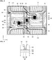
- FIG. 10 is a plan view showing some sub-pixels of the display device according to an embodiment of the present invention and FIG.11 is a cross-sectional view taken along line D-D' of FIG. 10 .
- first and second gate lines 40 and 42 extend in the first direction (x-axis direction).
- a touch routing line 28 is disposed to intersect the first and second gate lines 40 and 42.
- a first data line 50 is disposed to intersect the first and second gate lines 40 and 42.
- An area defined by the first data line 50, the first gate line 40 and the touch routing line 28 corresponds to a first sub-pixel 110.
- the touch routing line 28 is not connected to the touch electrode (common electrode) in which the first sub-pixel 110 is disposed and is connected to a touch electrode disposed at another position of the first column.
- the first sub-pixel 110 includes a thin film transistor 45 including the first gate line 40 serving as a gate electrode, a drain electrode 44 branched from the first data line 50, and a source electrode 46 opposite the drain electrode 44.
- the source electrode 46 of the thin film transistor 45 is in contact with a pixel electrode 60 through a contact hole 48.
- a common electrode 62 which forms electric fields along with the pixel electrode 60 is connected to a touch routing line which is not shown such that a common voltage and a touch driving voltage are applied to the common electrode 62.
- the common electrode 62 acts as a touch electrode disposed in the last row of the first column and thus is connected to common electrodes of neighboring sub-pixels, which are included in the same touch electrode, to be one body.
- the cross-sectional structure of a repair portion is described with reference to FIG. 11 .
- the touch routing line 28 overlaps with the pixel electrode 60 of the first sub-pixel 110 overlap but does not overlap with the common electrode connector 63 extended from the common electrode 62 of the first sub-pixel 110.
- the common electrode connector 63 of the first sub-pixel 110 is disposed such that it does not overlap with the touch routing line 28 and the pixel electrode 60 of the first sub-pixel 110 at the repair portion 99.
- a touch driving voltage is applied through the touch routing line 28 to a touch electrode other than the touch electrode in which the first sub-pixel 110 is disposed. Accordingly, when the common electrode connector 63 extended from the common electrode of the first sub-pixel 110 is connected to the touch routing line 28, touch driving voltages of different touch electrodes are applied to the common electrode 62 of the first sub-pixel 110 and thus a touch sensing error may be generated.
- the present invention can prevent generation of a touch sensing error by arranging the common electrode connector 63 of the first sub-pixel 110 such that the touch routing line 28 and the common electrode connector 63 do not overlap at the repair portion 99.
- FIG. 12 is a diagram showing shapes of the common electrode connector
- FIG. 13 is a diagram showing shapes of the touch routing line.
- FIG. 12(a) shows the common electrode connector 63 and the touch routing line 28 illustrated in FIG. 5 .
- the common electrode connector 63 includes a center part 290 having a first width W1 and line parts 291 which are extended from the center part 290 to one side and the other side and have a second width W2.
- the first width W1 of the center part 290 is wide such that a hole through which the common electrode connector is connected to the touch routing line can be formed.
- the line parts 291 serve as an interconnection line and are narrower than the first width W1.
- the line parts 291 are disposed such that they overlap with a center line C that passes through the center of the center part 290. That is, the line parts 291 are symmetrically disposed on the basis of the center line C of the center part 290.
- the line part 291 of the common electrode connector 63 is overlapped with the touch routing line 28.
- the repair portion 99 is positioned on the line part 291 of the common electrode connector 63. Therefore, when laser welding is performed on the repair portion 99, the pixel electrode 60 may be connected to the common electrode connector 63 as well as the touch routing line 28.
- FIG. 12(b) shows the common electrode connector 63 and the touch routing line 28 illustrated in FIG. 10 .
- the common electrode connector 63 includes a center part 290 having a first width W1 and line parts 291 which are extended from the center part 290 to one side and the other side and have a second width W2.
- the first width of the center part 290 is greater than the second width W2.
- a structural difference from the above-described common electrode connector shown in FIG. 12(a) is that the line parts 291 are disposed such that they do not overlap with the center line C that passes through the center of the center part 290.
- the line part 291 upwardly protruding from the center part 290 is disposed on the left of the center line C and the line part 291 downwardly protruding from the center part 290 is disposed on the right of the center line C on the basis of the center line C of the center part 290. That is, the line parts 291 are symmetrical on the basis of the center line C.
- the line part 291 of the common electrode connector 63 is spaced apart from the touch routing line 28 with a predetermined distance G1 interposed therebetween so that the line part 291 is not overlap with the touch routing line 28.
- the repair portion 99 is positioned on the touch routing line 28 that is not overlapped with the line part 291 of the common electrode connector 63. Therefore, when the laser welding is performed in the repair portion 99, the pixel electrode 60 is connected to the touch routing line 28. When the laser welding is performed, the line part 291 of the common electrode connector 63 is not connected to the touch routing line 28 because the line part 291 is spaced apart from the repair portion 99.
- the common electrode connector 63 having the aforementioned structures as shown in FIG. 12(b) does not overlap with the touch routing line 28 at the repair portion 99 as shown in FIG. 10 , and thus a touch sensing error can be prevented.
- FIG. 13(a) shows the touch routing line 28 illustrated in FIG. 5 .
- the touch routing line includes a center part 300 having a third width W3 and line parts 310 which are extended from the center part 300 to one side and the other side and have a fourth width W4.
- the third width W3 of the center part 300 is wide such that a hole through which the touch routing line is connected to a touch routing line disposed thereunder can be formed.
- the line parts 310 serve as an interconnection line and are narrower than the third width W3.
- the line parts 310 are disposed such that they overlap with a center line C that passes through the center of the center part 300. That is, the line parts 310 are symmetrically disposed on the basis of the center line C of the center part 300.
- the touch routing line has the same structure as the common electrode connector shown in FIG. 12(a) . Since the line part 310 is disposed on the center line C passing through the center of the center part 300, the line part 310 is overlapped the line part 291 of the common electrode connector portion 63. Therefore, when laser welding is performed on the repair portion 99, the touch routing line 28 may be shorted with the line part 291 of the common electrode connector 63.
- FIG. 13(b) shows the touch routing line illustrated in FIG. 10 .
- the touch routing line includes a center part 300 having a third width W3 and extended parts 320 which are extended from the center part 300 to one side and the other side and have a fifth width W5.
- the third width W3 of the center part 300 is greater than the fifth width W5.
- the fifth width W5 of the extended parts 320 is less than the third width W3 of the center part 300.
- the touch routing line includes line parts 310 which are respectively extended from the extended parts 320 and have a fourth width W4.
- the fourth width W4 of the line parts 310 is less than the third and fifth widths W3 and W5.
- the third width W3 is widest and the fourth width W4 is smallest.
- the fifth width W5 is less than the third width W3 and greater than the fourth width W4.
- the repair portion 99 may be positioned on a extended parts 320 of the touch routing line 28 that is not overlapped with the common electrode connector 63.
- a structural difference from the touch routing line shown in FIG. 12(b) is that the extended parts 320 for securing an area in which repairing can be performed are additionally provided between the center part 300 and the line parts 310. Accordingly, the touch routing line 28 having the aforementioned structure can provide an area in which laser welding can be performed on the touch routing line 28 and the pixel electrode 60 of the first sub-pixel 110 in the repair portion 99, as shown in FIG. 10 , thereby improving repair yield.
- FIG. 14 is a plan view showing some sub-pixels according to an embodiment of the present invention and FIG. 15 is a plan view showing common electrode connectors shown in FIG. 14 .
- the first gate line 40 and the second gate line 42 extend in the first direction (x-axis direction).
- the touch routing line 28 is disposed to intersect the first gate line 40 and the second gate line 42.
- the first data line 50 and the second data line 52 are disposed to intersect the first gate line 40 and the second gate line 42.
- An area defined by the first data line 50, the first gate line 40 and the touch routing line 28 corresponds to the first sub-pixel 110.
- An area defined by the second data line 52, the second gate line 42 and the touch routing line 28 corresponds to the second sub-pixel 120.
- the first sub-pixel 110 is included in the aforementioned touch electrode 36 disposed in the last row of the first column and the second sub-pixel 120 is included in the touch electrode 72 disposed in the last row of the second column on the basis of the touch routing line 28.
- the first sub-pixel 110 includes the thin film transistor 45 including the first gate line 40 serving as a gate electrode, the drain electrode 44 branched from the second data line 52, and the source electrode 46 opposite the drain electrode 44.
- the source electrode 46 of the thin film transistor 45 is in contact with the pixel electrode 60 through the contact hole 48.
- the common electrode 62 which forms electric fields along with the pixel electrode 60 is in contact with the touch routing line 28 through the via hole 64 included in a region overlapping with the touch routing line 28.
- a common voltage and a touch driving voltage are applied to the common electrode 62 through the touch routing line 28.
- the common electrode 62 acts as the touch electrode 36 disposed in the last row of the first column and thus is connected to a common electrode of a neighboring sub-pixel (sub-pixel disposed thereunder) to be one body.
- the common electrode 62 and the common electrode of the sub-pixel disposed thereunder are integrated into one body through the common electrode connector 63.
- the second sub-pixel 120 includes the thin film transistor 85 including the second gate line 42 serving as a gate electrode, the drain electrode 84 branched from the first data line 50, and the source electrode 86 opposite the drain electrode 84.
- the source electrode 86 of the thin film transistor 85 is in contact with the pixel electrode 90 through the contact hole 88.
- the common electrode 92 which forms electric fields along with the pixel electrode 90 is in contact with a touch routing line which is not shown.
- the common electrode 92 of the second sub-pixel 120 is connected to the touch routing line of the touch electrode 72 disposed in the last row of the second column to act as the touch electrode.
- the thin film transistor 45 of the first sub-pixel 110 is disposed adjacent to the second sub-pixel 120, and the thin film transistor 85 of the second sub-pixel 120 is disposed adjacent to the first sub-pixel 110. Accordingly, the pixel electrode 60 of the first sub-pixel 110 extends to intersect the touch routing line 28 and is connected to the thin film transistor 45. The pixel electrode 90 of the second sub-pixel 120 extends to intersect the touch routing line 28 and is connected to the thin film transistor 85. This is a structure formed according to an arrangement of sub-pixels for DRD.
- a third sub-pixel 130 is disposed under the second sub-pixel 120 and a fourth sub-pixel 140 is disposed on the left side of the second sub-pixel 120.
- a third gate line 340 and a fourth gate line 342 extend in the first direction (x-axis direction).
- the touch routing line 28 is disposed to intersect the third and fourth gate lines 340 and 342.
- the first data line 50 and the second data line 52 are disposed to intersect the third and fourth gate lines 340 and 342.
- An area defined by the first data line 50, the third gate line 340 and the touch routing line 28 corresponds to a fourth sub-pixel 140.
- An area defined by the second data line 52, the fourth gate line 342 and the touch routing line 28 corresponds to a third sub-pixel 130.
- the touch routing line 28 is connected to a touch electrode (common electrode) in which the fourth sub-pixel 140 is disposed and is not connected to a touch electrode (common electrode) in which the third sub-pixel 130 is disposed.
- the third sub-pixel 130 includes a thin film transistor 345 including the fourth gate line 342 serving as a gate electrode, a drain electrode 344 branched from the second data line 52, and a source electrode 346 opposite the drain electrode 344.
- the source electrode 346 of the thin film transistor 345 is in contact with a pixel electrode 360 through a contact hole 348.
- a common electrode 362 which forms electric fields along with the pixel electrode 360 is connected to a touch routing line which is not shown and thus a common voltage and a touch driving voltage are applied to the common electrode 362.
- the common electrode 362 is included in the touch electrode 72 and thus connected to common electrodes of neighboring sub-pixels, which are included in the same touch electrode, to be one body.
- the fourth sub-pixel 140 includes a thin film transistor 385 including the third gate line 340 serving as a gate electrode, a drain electrode 384 branched from the first data line 50, and a source electrode 386 opposite the drain electrode 384.
- the source electrode 386 of the thin film transistor 385 is in contact with a pixel electrode 390 through a contact hole 388.
- a common electrode 392 which forms electric fields along with the pixel electrode 390 is connected to the touch routing line 28 such that a common voltage and a touch driving voltage are applied to the common electrode 392.
- the common electrode 392 is included in the touch electrode 36 and thus connected to common electrodes of neighboring sub-pixels, which are included in the same touch electrode, to be one body.
- the common electrode 62 of the first sub-pixel comes into contact with the touch routing line 28 through the via hole 64 included in a region overlapping with the touch routing line 28 through the common electrode connector 63.
- the common electrode connector 63 is formed in a different shape from the aforementioned common electrode connector 63 shown in FIG. 12(b) .
- the corresponding touch routing line 28 is connected to the touch electrode 36 disposed on the left of the touch routing line 28, and when this is connected to the touch electrode 72 disposed on the right thereof, touch error is generated. Accordingly, one side of the common electrode connector 63 is connected to the common electrode 62 of the first sub-pixel 110 and the other side thereof is connected to the touch routing line 28 without being connected to common electrodes of other sub-pixels in the present invention.
- the common electrode connector includes a center part 290 having a first width W1 and a line part 291 which are extended from the center part 290 to one side and has a second width W2.
- the first width W1 of the center part 290 is greater than the second width W2.
- a structural difference from the aforementioned common electrode connector shown in FIG. 12(b) is that the line part 291 is disposed on the left side of the center line C and formed only on one side of the center part 290.
- the touch routing line 28 is connected to the touch electrode 36 disposed on the left side of the touch routing line 28 and thus the line part 291 can be disposed on the left side to be connected to the common electrode 62 of the first sub-pixel 110 disposed on the left side of the touch routing line 28.
- the line part 291 is disposed only on one side of the center part 290 to prevent laser radiation time increase and processability deterioration during repairing performed in the repair portion 99 under the via hole 64 according to the common electrode connector disposed at the uppermost level.
- the common electrode 392 of the fourth sub-pixel 140 comes into contact with the touch routing line 28 through the via hole 364 included in a region overlapping with the touch routing line 28 through a common electrode connector 363.
- the common electrode connector 363 is formed in a different shape from the aforementioned common electrode connector 63 shown in FIG. 12(b) .
- the corresponding touch routing line 28 is connected to the touch electrode 36 disposed on the left of the touch routing line 28, and when this is connected to the touch electrode 72 disposed on the right thereof, touch error is generated.
- the common electrode connector 63 may be formed in a structure in which the common electrode connector 63 connects the common electrode 62 of the first sub-pixel 110 to the common electrode of the fourth sub-pixel 140 in the present invention.
- the common electrode connector includes a center part 290 having a first width W1 and line parts 291 which are extended from the center part 290 to one side and the other side and have a second width W2.
- the first width W1 of the center part 290 is greater than the second width W2.
- a structural difference from the aforementioned common electrode connector shown in FIG. 12(b) is that the line parts 291 are disposed on the left side of the center line C.
- both the line parts 291 can be disposed on the left side to connect the common electrode 62 of the first sub-pixel 110 disposed on the left side of the touch routing line 28 to the common electrode 392 of the fourth sub-pixel 140.
- the display device includes a common electrode connector which is formed in various structures for each touch electrode area and thus can prevent touch sensing error and allow a repair process to be performed.
Landscapes
- Physics & Mathematics (AREA)
- Nonlinear Science (AREA)
- Mathematical Physics (AREA)
- Chemical & Material Sciences (AREA)
- Crystallography & Structural Chemistry (AREA)
- General Physics & Mathematics (AREA)
- Optics & Photonics (AREA)
- Engineering & Computer Science (AREA)
- Microelectronics & Electronic Packaging (AREA)
- Devices For Indicating Variable Information By Combining Individual Elements (AREA)
- Geometry (AREA)
- Liquid Crystal (AREA)
Claims (15)
- Anzeigevorrichtung des Berührungstyps, die Folgendes umfasst:ein Substrat (100);eine erste Datenleitung (50), die auf dem Substrat (100) angeordnet ist;eine Berührungslenkungsleitung (28), die parallel zu der ersten Datenleitung (50) angeordnet ist;eine erste Gate-Leitung (40), die die erste Datenleitung (50) und die Berührungslenkungsleitung (28) schneidet; undein erstes Unterpixel (110), das in Übereinstimmung mit Schnittpunkten der ersten Datenleitung (50) und der Berührungslenkungsleitung (28) mit der ersten Gate-Leitung (40) definiert ist, wobeidas erste Unterpixel (110) einen Dünnschichttransistor (45), der an dem Schnittpunkt der ersten Datenleitung (50) und der ersten Gate-Leitung (40) angeordnet ist, eine Pixel-Elektrode (60), die mit dem Dünnschichttransistor (45) verbunden ist, und eine gemeinsame Elektrode (62), die mit der Pixel-Elektrode (60) überlappt, enthält,die gemeinsame Elektrode (62) einen Verbinder (63) für die gemeinsame Elektrode, der sich zu einem weiteren Unterpixel (120, 140) erstreckt, enthält,die Berührungslenkungsleitung (28) und der Verbinder (63) für die gemeinsame Elektrode so angeordnet sind, dass sie miteinander überlappen,ein Reparaturabschnitt, wo ein Laserschweißen ausgeführt werden kann, in einem Bereich enthalten ist, in dem die Pixelelektrode (60) und die Berührungslenkungsleitung (28) überlappen, undder Verbinder (63) für die gemeinsame Elektrode mit dem Reparaturabschnitt (99) nicht überlappt.
- Anzeigevorrichtung nach Anspruch 1, wobeidas weitere Unterpixel ein zweites Unterpixel (120) ist, das zu dem ersten Unterpixel (110) benachbart ist,die Anzeigevorrichtung eine zweite Datenleitung (52) und eine zweite Gate-Leitung (42) aufweist, die auf dem Substrat (100) angeordnet sind,die erste und die zweite Datenleitung (50, 52) zueinander parallel angeordnet sind,die erste und die zweite Gate-Leitung (40, 42) zueinander parallel angeordnet sind,die Berührungslenkungsleitung (28) zwischen der ersten und der zweiten Datenleitung (50, 52) und parallel zu der ersten Datenleitung (50) angeordnet ist unddas zweite Unterpixel (120) einen Dünnschichttransistor (85), der an dem Schnittpunkt der zweiten Datenleitung (52) und der zweiten Gate-Leitung (42) angeordnet ist, eine Pixel-Elektrode (90), die mit dem Dünnschichttransistor (85) verbunden ist, und eine gemeinsame Elektrode (92), die mit der Pixel-Elektrode (90) überlappt, enthält.
- Anzeigevorrichtung nach Anspruch 1, die eine zweite Datenleitung (52) und eine zweite Gate-Leitung (42), die auf dem Substrat (100) angeordnet sind, umfasst, wobeidie erste und die zweite Datenleitung (50, 52) zueinander parallel angeordnet sind, die erste und die zweite Gate-Leitung (40, 42) zueinander parallel angeordnet sind, die Berührungslenkungsleitung (28) zwischen der ersten und der zweiten Datenleitung (50, 52) und parallel zu der ersten Datenleitung (50) angeordnet ist;ein zweites Unterpixel (120) in Übereinstimmung mit Schnittpunkten der zweiten Datenleitung (52) und der Berührungslenkungsleitung (28) mit der zweiten Gate-Leitung (42) definiert ist;das zweite Unterpixel (120) einen Dünnschichttransistor (85), der an dem Schnittpunkt der zweiten Datenleitung (52) und der zweiten Gate-Leitung (42) angeordnet ist, eine Pixel-Elektrode (90), die mit dem Dünnschichttransistor (85) verbunden ist, und eine gemeinsame Elektrode (92), die mit der Pixel-Elektrode (90) überlappt, enthält; unddas weitere Unterpixel ein drittes Unterpixel (140) ist, das in einer Richtung, in der sich die Berührungslenkungsleitung (28) erstreckt, in der Nähe des ersten Unterpixels (110) angeordnet ist.
- Anzeigevorrichtung nach Anspruch 3, wobei die gemeinsame Elektrode (62) des ersten Unterpixels (110) in Bezug auf die gemeinsame Elektrode (92) des zweiten Unterpixels (120) über den Verbinder (63) für die gemeinsame Elektrode elektrisch kurzgeschlossen ist.
- Anzeigevorrichtung nach einem der Ansprüche 1 bis 4, wobei die Berührungslenkungsleitung (28) konfiguriert ist, an eine Berührungselektrode, die von einer in dem ersten Unterpixel (110) angeordneten Berührungselektrode verschieden ist, eine Berührungsansteuerspannung anzulegen.
- Anzeigevorrichtung nach einem der Ansprüche 1 bis 5, wobei der Verbinder (63) für die gemeinsame Elektrode einen Mittelteil (290) und wenigstens einen Linienteil (291), der sich von dem Mittelteil (290) zu einer ersten Seite erstreckt, aufweist.
- Anzeigevorrichtung nach Anspruch 6, wobei der Linienteil (291) auf einer Seite einer Mittellinie des Mittelteils (290) angeordnet ist.
- Anzeigevorrichtung nach den Ansprüchen 6 oder 7, wobei der Verbinder (63) für die gemeinsame Elektrode einen weiteren Linienteil (291) enthält, der sich von dem Mittelteil (290) zu einer zweiten Seite erstreckt, wobei der Mittelteil zwischen der ersten und der zweiten Seite angeordnet ist.
- Anzeigevorrichtung nach Anspruch 8, wobei die Linienteile (291) des Verbinders (63) für die gemeinsame Elektrode in Bezug auf die Mittellinie (C) des Mittelteils (290) des Verbinders (63) für die gemeinsame Elektrode auf derselben Seite oder auf unterschiedlichen Seiten angeordnet sind.
- Anzeigevorrichtung nach einem der Ansprüche 6 bis 9, wobei der Mittelteil (290) des Verbinders (63) für die gemeinsame Elektrode eine erste Breite (W1) besitzt und der wenigstens eine Linienteil (291) des Verbinders (63) für die gemeinsame Elektrode eine zweite Breite (W2) besitzt, wobei die erste Breite (W1) größer als die zweite Breite (W2) ist.
- Anzeigevorrichtung nach einem der Ansprüche 1 bis 10, wobei die Berührungslenkungsleitung (28) einen Mittelteil (300), Verlängerungsteile (320), die sich zu einer Seite bzw. zu der anderen Seite des Mittelteil (300) erstrecken, und Linienteile (310), die sich jeweils von den Verlängerungsteilen (320) erstrecken, umfasst.
- Anzeigevorrichtung nach Anspruch 11, wobei der Mittelteil (300) der Berührungslenkungsleitung (28) eine dritte Breite (W3) besitzt, die Verlängerungsteile (320) der Berührungslenkungsleitung (28) eine fünfte Breite (W5) besitzen und die Linienteile (310) der Berührungslenkungsleitung (28) eine vierte Breite (W4) besitzen,
wobei die dritte Breite (W3) größer als die vierte Breite (W4) und die fünfte Breite (W5) ist und die fünfte Breite (W5) größer als die vierte Breite (W4) ist. - Anzeigevorrichtung nach Anspruch 11 oder 12, wobei die Linienteile (291) des Verbinders (63) für die gemeinsame Elektrode mit den Linienteilen (310) der Berührungslenkungsleitung (28) nicht überlappen.
- Anzeigevorrichtung nach einem der Ansprüche 11 bis 13, wobei der Mittelteil (210) des Verbinders (63) für die gemeinsame Elektrode und der Mittelteil (300) der Berührungslenkungsleitung (28) überlappen.
- Anzeigevorrichtung einem der Ansprüche 1 bis 12, wobei die Berührungslenkungsleitung (28) in Bezug auf die gemeinsame Elektrode (62) elektrisch kurzgeschlossen ist.
Applications Claiming Priority (1)
| Application Number | Priority Date | Filing Date | Title |
|---|---|---|---|
| KR1020180171792A KR102595180B1 (ko) | 2018-12-28 | 2018-12-28 | 표시장치 |
Publications (2)
| Publication Number | Publication Date |
|---|---|
| EP3674789A1 EP3674789A1 (de) | 2020-07-01 |
| EP3674789B1 true EP3674789B1 (de) | 2021-11-24 |
Family
ID=68965781
Family Applications (1)
| Application Number | Title | Priority Date | Filing Date |
|---|---|---|---|
| EP19217832.5A Active EP3674789B1 (de) | 2018-12-28 | 2019-12-19 | Anzeigevorrichtung |
Country Status (4)
| Country | Link |
|---|---|
| US (1) | US10877344B2 (de) |
| EP (1) | EP3674789B1 (de) |
| KR (1) | KR102595180B1 (de) |
| CN (1) | CN111381392B (de) |
Families Citing this family (4)
| Publication number | Priority date | Publication date | Assignee | Title |
|---|---|---|---|---|
| KR102831356B1 (ko) * | 2019-10-04 | 2025-07-08 | 삼성디스플레이 주식회사 | 표시 장치 |
| KR102904102B1 (ko) * | 2020-09-25 | 2025-12-26 | 삼성디스플레이 주식회사 | 표시 장치 |
| TWI753660B (zh) * | 2020-11-19 | 2022-01-21 | 友達光電股份有限公司 | 顯示面板 |
| CN118737081B (zh) * | 2024-07-01 | 2025-10-03 | Tcl华星光电技术有限公司 | 显示面板及显示装置 |
Family Cites Families (14)
| Publication number | Priority date | Publication date | Assignee | Title |
|---|---|---|---|---|
| JP2002091342A (ja) * | 2000-07-10 | 2002-03-27 | Toshiba Corp | マトリクスアレイ基板 |
| US7304692B2 (en) * | 2004-06-02 | 2007-12-04 | Chunghwa Picture Tubes, Ltd. | Liquid crystal display with defect reparability |
| TWI349818B (en) * | 2007-03-12 | 2011-10-01 | Prime View Int Co Ltd | Repairing method and structure of display electrode |
| KR101327847B1 (ko) * | 2007-03-13 | 2013-11-11 | 엘지디스플레이 주식회사 | 액정표시장치와 그 제조방법 |
| US10312374B2 (en) * | 2012-10-01 | 2019-06-04 | Sharp Kabushiki Kaisha | Circuit board and display device |
| CN104461147B (zh) * | 2014-12-12 | 2017-05-17 | 深圳市华星光电技术有限公司 | 显示面板及其修复方法 |
| CN204595382U (zh) * | 2015-05-08 | 2015-08-26 | 厦门天马微电子有限公司 | 阵列基板及液晶显示面板及装置及已修复阵列基板 |
| CN104898343B (zh) * | 2015-06-30 | 2017-12-22 | 重庆京东方光电科技有限公司 | 阵列基板、显示面板及显示装置 |
| CN105116590B (zh) | 2015-09-28 | 2018-06-08 | 京东方科技集团股份有限公司 | 阵列基板、显示装置及阵列基板修复方法 |
| CN105572935B (zh) * | 2015-12-16 | 2019-01-15 | 上海天马微电子有限公司 | 一种触控显示面板和显示装置 |
| KR102401354B1 (ko) * | 2015-12-31 | 2022-05-25 | 엘지디스플레이 주식회사 | 터치 센서 내장형 표시장치 |
| KR102578806B1 (ko) * | 2016-10-31 | 2023-09-14 | 엘지디스플레이 주식회사 | 터치형 표시패널 및 그의 쇼트 리페어 방법 |
| KR102693166B1 (ko) * | 2016-12-02 | 2024-08-09 | 티씨엘 차이나 스타 옵토일렉트로닉스 테크놀로지 컴퍼니 리미티드 | 표시 패널 및 이를 리페어하기 위한 방법 |
| JP2019184945A (ja) * | 2018-04-16 | 2019-10-24 | シャープ株式会社 | 配線基板及び表示装置 |
-
2018
- 2018-12-28 KR KR1020180171792A patent/KR102595180B1/ko active Active
-
2019
- 2019-12-17 US US16/717,488 patent/US10877344B2/en active Active
- 2019-12-19 EP EP19217832.5A patent/EP3674789B1/de active Active
- 2019-12-20 CN CN201911345359.1A patent/CN111381392B/zh active Active
Also Published As
| Publication number | Publication date |
|---|---|
| CN111381392B (zh) | 2022-11-08 |
| CN111381392A (zh) | 2020-07-07 |
| US20200209697A1 (en) | 2020-07-02 |
| EP3674789A1 (de) | 2020-07-01 |
| KR20200081852A (ko) | 2020-07-08 |
| KR102595180B1 (ko) | 2023-10-27 |
| US10877344B2 (en) | 2020-12-29 |
Similar Documents
| Publication | Publication Date | Title |
|---|---|---|
| CN101587270B (zh) | 液晶显示器 | |
| US9190003B2 (en) | Display apparatus and method of manufacturing the same | |
| CN1959480B (zh) | 液晶显示器 | |
| JP5414974B2 (ja) | 液晶表示装置 | |
| KR101654834B1 (ko) | 박막 트랜지스터 표시판 및 그 제조 방법 | |
| KR101204365B1 (ko) | 액정 표시 패널 및 그 제조 방법 | |
| EP3674789B1 (de) | Anzeigevorrichtung | |
| US20080180372A1 (en) | Display device | |
| JP2014119754A (ja) | 液晶ディスプレイ装置 | |
| US10621944B2 (en) | Gate voltage generation circuit, transistor substrate and display device | |
| US20180182317A1 (en) | Driver structure for rgbw four-color panel | |
| JP4277894B2 (ja) | 電気光学装置、駆動回路および電子機器 | |
| KR20140071042A (ko) | 액정표시장치 | |
| KR20110107659A (ko) | 액정표시장치 | |
| US20170115522A1 (en) | Liquid crystal display having increased resistance to short circuits and method of manufacturing the same | |
| JP2007226243A (ja) | 液晶表示装置 | |
| KR101046927B1 (ko) | 박막 트랜지스터 표시판 | |
| KR102039410B1 (ko) | 액정 디스플레이 장치와 이의 구동방법 | |
| TWI406068B (zh) | 陣列基板及具有此陣列基板之顯示器裝置 | |
| KR102763622B1 (ko) | 범프를 포함하는 표시장치 | |
| US10891892B2 (en) | Display device | |
| KR20160012789A (ko) | 액정표시장치 | |
| KR102524416B1 (ko) | 표시장치 | |
| KR102605294B1 (ko) | 표시장치 | |
| KR20170033934A (ko) | 협 베젤 구조를 갖는 대형 액정 표시장치 |
Legal Events
| Date | Code | Title | Description |
|---|---|---|---|
| PUAI | Public reference made under article 153(3) epc to a published international application that has entered the european phase |
Free format text: ORIGINAL CODE: 0009012 |
|
| STAA | Information on the status of an ep patent application or granted ep patent |
Free format text: STATUS: REQUEST FOR EXAMINATION WAS MADE |
|
| 17P | Request for examination filed |
Effective date: 20191219 |
|
| AK | Designated contracting states |
Kind code of ref document: A1 Designated state(s): AL AT BE BG CH CY CZ DE DK EE ES FI FR GB GR HR HU IE IS IT LI LT LU LV MC MK MT NL NO PL PT RO RS SE SI SK SM TR |
|
| AX | Request for extension of the european patent |
Extension state: BA ME |
|
| RBV | Designated contracting states (corrected) |
Designated state(s): AL AT BE BG CH CY CZ DE DK EE ES FI FR GB GR HR HU IE IS IT LI LT LU LV MC MK MT NL NO PL PT RO RS SE SI SK SM TR |
|
| GRAP | Despatch of communication of intention to grant a patent |
Free format text: ORIGINAL CODE: EPIDOSNIGR1 |
|
| STAA | Information on the status of an ep patent application or granted ep patent |
Free format text: STATUS: GRANT OF PATENT IS INTENDED |
|
| INTG | Intention to grant announced |
Effective date: 20210714 |
|
| GRAA | (expected) grant |
Free format text: ORIGINAL CODE: 0009210 |
|
| STAA | Information on the status of an ep patent application or granted ep patent |
Free format text: STATUS: THE PATENT HAS BEEN GRANTED |
|
| GRAS | Grant fee paid |
Free format text: ORIGINAL CODE: EPIDOSNIGR3 |
|
| AK | Designated contracting states |
Kind code of ref document: B1 Designated state(s): AL AT BE BG CH CY CZ DE DK EE ES FI FR GB GR HR HU IE IS IT LI LT LU LV MC MK MT NL NO PL PT RO RS SE SI SK SM TR |
|
| REG | Reference to a national code |
Ref country code: GB Ref legal event code: FG4D |
|
| REG | Reference to a national code |
Ref country code: AT Ref legal event code: REF Ref document number: 1450296 Country of ref document: AT Kind code of ref document: T Effective date: 20211215 |
|
| REG | Reference to a national code |
Ref country code: DE Ref legal event code: R096 Ref document number: 602019009523 Country of ref document: DE |
|
| REG | Reference to a national code |
Ref country code: IE Ref legal event code: FG4D |
|
| REG | Reference to a national code |
Ref country code: LT Ref legal event code: MG9D |
|
| REG | Reference to a national code |
Ref country code: NL Ref legal event code: MP Effective date: 20211124 |
|
| REG | Reference to a national code |
Ref country code: AT Ref legal event code: MK05 Ref document number: 1450296 Country of ref document: AT Kind code of ref document: T Effective date: 20211124 |
|
| PG25 | Lapsed in a contracting state [announced via postgrant information from national office to epo] |
Ref country code: RS Free format text: LAPSE BECAUSE OF FAILURE TO SUBMIT A TRANSLATION OF THE DESCRIPTION OR TO PAY THE FEE WITHIN THE PRESCRIBED TIME-LIMIT Effective date: 20211124 Ref country code: LT Free format text: LAPSE BECAUSE OF FAILURE TO SUBMIT A TRANSLATION OF THE DESCRIPTION OR TO PAY THE FEE WITHIN THE PRESCRIBED TIME-LIMIT Effective date: 20211124 Ref country code: FI Free format text: LAPSE BECAUSE OF FAILURE TO SUBMIT A TRANSLATION OF THE DESCRIPTION OR TO PAY THE FEE WITHIN THE PRESCRIBED TIME-LIMIT Effective date: 20211124 Ref country code: BG Free format text: LAPSE BECAUSE OF FAILURE TO SUBMIT A TRANSLATION OF THE DESCRIPTION OR TO PAY THE FEE WITHIN THE PRESCRIBED TIME-LIMIT Effective date: 20220224 Ref country code: AT Free format text: LAPSE BECAUSE OF FAILURE TO SUBMIT A TRANSLATION OF THE DESCRIPTION OR TO PAY THE FEE WITHIN THE PRESCRIBED TIME-LIMIT Effective date: 20211124 |
|
| PG25 | Lapsed in a contracting state [announced via postgrant information from national office to epo] |
Ref country code: IS Free format text: LAPSE BECAUSE OF FAILURE TO SUBMIT A TRANSLATION OF THE DESCRIPTION OR TO PAY THE FEE WITHIN THE PRESCRIBED TIME-LIMIT Effective date: 20220324 Ref country code: SE Free format text: LAPSE BECAUSE OF FAILURE TO SUBMIT A TRANSLATION OF THE DESCRIPTION OR TO PAY THE FEE WITHIN THE PRESCRIBED TIME-LIMIT Effective date: 20211124 Ref country code: PT Free format text: LAPSE BECAUSE OF FAILURE TO SUBMIT A TRANSLATION OF THE DESCRIPTION OR TO PAY THE FEE WITHIN THE PRESCRIBED TIME-LIMIT Effective date: 20220324 Ref country code: PL Free format text: LAPSE BECAUSE OF FAILURE TO SUBMIT A TRANSLATION OF THE DESCRIPTION OR TO PAY THE FEE WITHIN THE PRESCRIBED TIME-LIMIT Effective date: 20211124 Ref country code: NO Free format text: LAPSE BECAUSE OF FAILURE TO SUBMIT A TRANSLATION OF THE DESCRIPTION OR TO PAY THE FEE WITHIN THE PRESCRIBED TIME-LIMIT Effective date: 20220224 Ref country code: NL Free format text: LAPSE BECAUSE OF FAILURE TO SUBMIT A TRANSLATION OF THE DESCRIPTION OR TO PAY THE FEE WITHIN THE PRESCRIBED TIME-LIMIT Effective date: 20211124 Ref country code: LV Free format text: LAPSE BECAUSE OF FAILURE TO SUBMIT A TRANSLATION OF THE DESCRIPTION OR TO PAY THE FEE WITHIN THE PRESCRIBED TIME-LIMIT Effective date: 20211124 Ref country code: HR Free format text: LAPSE BECAUSE OF FAILURE TO SUBMIT A TRANSLATION OF THE DESCRIPTION OR TO PAY THE FEE WITHIN THE PRESCRIBED TIME-LIMIT Effective date: 20211124 Ref country code: GR Free format text: LAPSE BECAUSE OF FAILURE TO SUBMIT A TRANSLATION OF THE DESCRIPTION OR TO PAY THE FEE WITHIN THE PRESCRIBED TIME-LIMIT Effective date: 20220225 Ref country code: ES Free format text: LAPSE BECAUSE OF FAILURE TO SUBMIT A TRANSLATION OF THE DESCRIPTION OR TO PAY THE FEE WITHIN THE PRESCRIBED TIME-LIMIT Effective date: 20211124 |
|
| PG25 | Lapsed in a contracting state [announced via postgrant information from national office to epo] |
Ref country code: SM Free format text: LAPSE BECAUSE OF FAILURE TO SUBMIT A TRANSLATION OF THE DESCRIPTION OR TO PAY THE FEE WITHIN THE PRESCRIBED TIME-LIMIT Effective date: 20211124 Ref country code: SK Free format text: LAPSE BECAUSE OF FAILURE TO SUBMIT A TRANSLATION OF THE DESCRIPTION OR TO PAY THE FEE WITHIN THE PRESCRIBED TIME-LIMIT Effective date: 20211124 Ref country code: RO Free format text: LAPSE BECAUSE OF FAILURE TO SUBMIT A TRANSLATION OF THE DESCRIPTION OR TO PAY THE FEE WITHIN THE PRESCRIBED TIME-LIMIT Effective date: 20211124 Ref country code: EE Free format text: LAPSE BECAUSE OF FAILURE TO SUBMIT A TRANSLATION OF THE DESCRIPTION OR TO PAY THE FEE WITHIN THE PRESCRIBED TIME-LIMIT Effective date: 20211124 Ref country code: DK Free format text: LAPSE BECAUSE OF FAILURE TO SUBMIT A TRANSLATION OF THE DESCRIPTION OR TO PAY THE FEE WITHIN THE PRESCRIBED TIME-LIMIT Effective date: 20211124 Ref country code: CZ Free format text: LAPSE BECAUSE OF FAILURE TO SUBMIT A TRANSLATION OF THE DESCRIPTION OR TO PAY THE FEE WITHIN THE PRESCRIBED TIME-LIMIT Effective date: 20211124 |
|
| REG | Reference to a national code |
Ref country code: DE Ref legal event code: R097 Ref document number: 602019009523 Country of ref document: DE |
|
| PG25 | Lapsed in a contracting state [announced via postgrant information from national office to epo] |
Ref country code: MC Free format text: LAPSE BECAUSE OF FAILURE TO SUBMIT A TRANSLATION OF THE DESCRIPTION OR TO PAY THE FEE WITHIN THE PRESCRIBED TIME-LIMIT Effective date: 20211124 |
|
| REG | Reference to a national code |
Ref country code: BE Ref legal event code: MM Effective date: 20211231 |
|
| PLBE | No opposition filed within time limit |
Free format text: ORIGINAL CODE: 0009261 |
|
| STAA | Information on the status of an ep patent application or granted ep patent |
Free format text: STATUS: NO OPPOSITION FILED WITHIN TIME LIMIT |
|
| PG25 | Lapsed in a contracting state [announced via postgrant information from national office to epo] |
Ref country code: LU Free format text: LAPSE BECAUSE OF NON-PAYMENT OF DUE FEES Effective date: 20211219 Ref country code: IE Free format text: LAPSE BECAUSE OF NON-PAYMENT OF DUE FEES Effective date: 20211219 Ref country code: AL Free format text: LAPSE BECAUSE OF FAILURE TO SUBMIT A TRANSLATION OF THE DESCRIPTION OR TO PAY THE FEE WITHIN THE PRESCRIBED TIME-LIMIT Effective date: 20211124 |
|
| 26N | No opposition filed |
Effective date: 20220825 |
|
| PG25 | Lapsed in a contracting state [announced via postgrant information from national office to epo] |
Ref country code: SI Free format text: LAPSE BECAUSE OF FAILURE TO SUBMIT A TRANSLATION OF THE DESCRIPTION OR TO PAY THE FEE WITHIN THE PRESCRIBED TIME-LIMIT Effective date: 20211124 Ref country code: BE Free format text: LAPSE BECAUSE OF NON-PAYMENT OF DUE FEES Effective date: 20211231 |
|
| PG25 | Lapsed in a contracting state [announced via postgrant information from national office to epo] |
Ref country code: IT Free format text: LAPSE BECAUSE OF FAILURE TO SUBMIT A TRANSLATION OF THE DESCRIPTION OR TO PAY THE FEE WITHIN THE PRESCRIBED TIME-LIMIT Effective date: 20211124 |
|
| PG25 | Lapsed in a contracting state [announced via postgrant information from national office to epo] |
Ref country code: CY Free format text: LAPSE BECAUSE OF FAILURE TO SUBMIT A TRANSLATION OF THE DESCRIPTION OR TO PAY THE FEE WITHIN THE PRESCRIBED TIME-LIMIT Effective date: 20211124 |
|
| PG25 | Lapsed in a contracting state [announced via postgrant information from national office to epo] |
Ref country code: HU Free format text: LAPSE BECAUSE OF FAILURE TO SUBMIT A TRANSLATION OF THE DESCRIPTION OR TO PAY THE FEE WITHIN THE PRESCRIBED TIME-LIMIT; INVALID AB INITIO Effective date: 20191219 |
|
| REG | Reference to a national code |
Ref country code: CH Ref legal event code: PL |
|
| PG25 | Lapsed in a contracting state [announced via postgrant information from national office to epo] |
Ref country code: LI Free format text: LAPSE BECAUSE OF NON-PAYMENT OF DUE FEES Effective date: 20221231 Ref country code: CH Free format text: LAPSE BECAUSE OF NON-PAYMENT OF DUE FEES Effective date: 20221231 |
|
| PG25 | Lapsed in a contracting state [announced via postgrant information from national office to epo] |
Ref country code: MK Free format text: LAPSE BECAUSE OF FAILURE TO SUBMIT A TRANSLATION OF THE DESCRIPTION OR TO PAY THE FEE WITHIN THE PRESCRIBED TIME-LIMIT Effective date: 20211124 |
|
| PG25 | Lapsed in a contracting state [announced via postgrant information from national office to epo] |
Ref country code: TR Free format text: LAPSE BECAUSE OF FAILURE TO SUBMIT A TRANSLATION OF THE DESCRIPTION OR TO PAY THE FEE WITHIN THE PRESCRIBED TIME-LIMIT Effective date: 20211124 |
|
| PG25 | Lapsed in a contracting state [announced via postgrant information from national office to epo] |
Ref country code: MT Free format text: LAPSE BECAUSE OF FAILURE TO SUBMIT A TRANSLATION OF THE DESCRIPTION OR TO PAY THE FEE WITHIN THE PRESCRIBED TIME-LIMIT Effective date: 20211124 |
|
| PGFP | Annual fee paid to national office [announced via postgrant information from national office to epo] |
Ref country code: DE Payment date: 20251020 Year of fee payment: 7 |
|
| PGFP | Annual fee paid to national office [announced via postgrant information from national office to epo] |
Ref country code: GB Payment date: 20251023 Year of fee payment: 7 |
|
| PGFP | Annual fee paid to national office [announced via postgrant information from national office to epo] |
Ref country code: FR Payment date: 20251021 Year of fee payment: 7 |