EP3671832B1 - Halbleiter-chip-scale-gehäuse - Google Patents
Halbleiter-chip-scale-gehäuse Download PDFInfo
- Publication number
- EP3671832B1 EP3671832B1 EP18212913.0A EP18212913A EP3671832B1 EP 3671832 B1 EP3671832 B1 EP 3671832B1 EP 18212913 A EP18212913 A EP 18212913A EP 3671832 B1 EP3671832 B1 EP 3671832B1
- Authority
- EP
- European Patent Office
- Prior art keywords
- semiconductor chip
- chip scale
- layer
- scale package
- insulating layer
- Prior art date
- Legal status (The legal status is an assumption and is not a legal conclusion. Google has not performed a legal analysis and makes no representation as to the accuracy of the status listed.)
- Active
Links
Images

Classifications
-
- H—ELECTRICITY
- H10—SEMICONDUCTOR DEVICES; ELECTRIC SOLID-STATE DEVICES NOT OTHERWISE PROVIDED FOR
- H10W—GENERIC PACKAGES, INTERCONNECTIONS, CONNECTORS OR OTHER CONSTRUCTIONAL DETAILS OF DEVICES COVERED BY CLASS H10
- H10W46/00—Marks applied to devices, e.g. for alignment or identification
-
- H—ELECTRICITY
- H10—SEMICONDUCTOR DEVICES; ELECTRIC SOLID-STATE DEVICES NOT OTHERWISE PROVIDED FOR
- H10W—GENERIC PACKAGES, INTERCONNECTIONS, CONNECTORS OR OTHER CONSTRUCTIONAL DETAILS OF DEVICES COVERED BY CLASS H10
- H10W74/00—Encapsulations, e.g. protective coatings
- H10W74/01—Manufacture or treatment
- H10W74/014—Manufacture or treatment using batch processing
-
- H—ELECTRICITY
- H10—SEMICONDUCTOR DEVICES; ELECTRIC SOLID-STATE DEVICES NOT OTHERWISE PROVIDED FOR
- H10W—GENERIC PACKAGES, INTERCONNECTIONS, CONNECTORS OR OTHER CONSTRUCTIONAL DETAILS OF DEVICES COVERED BY CLASS H10
- H10W74/00—Encapsulations, e.g. protective coatings
- H10W74/10—Encapsulations, e.g. protective coatings characterised by their shape or disposition
- H10W74/111—Encapsulations, e.g. protective coatings characterised by their shape or disposition the semiconductor body being completely enclosed
- H10W74/129—Encapsulations, e.g. protective coatings characterised by their shape or disposition the semiconductor body being completely enclosed forming a chip-scale package [CSP]
-
- H—ELECTRICITY
- H10—SEMICONDUCTOR DEVICES; ELECTRIC SOLID-STATE DEVICES NOT OTHERWISE PROVIDED FOR
- H10W—GENERIC PACKAGES, INTERCONNECTIONS, CONNECTORS OR OTHER CONSTRUCTIONAL DETAILS OF DEVICES COVERED BY CLASS H10
- H10W46/00—Marks applied to devices, e.g. for alignment or identification
- H10W46/101—Marks applied to devices, e.g. for alignment or identification characterised by the type of information, e.g. logos or symbols
- H10W46/103—Marks applied to devices, e.g. for alignment or identification characterised by the type of information, e.g. logos or symbols alphanumeric information, e.g. words, letters or serial numbers
-
- H—ELECTRICITY
- H10—SEMICONDUCTOR DEVICES; ELECTRIC SOLID-STATE DEVICES NOT OTHERWISE PROVIDED FOR
- H10W—GENERIC PACKAGES, INTERCONNECTIONS, CONNECTORS OR OTHER CONSTRUCTIONAL DETAILS OF DEVICES COVERED BY CLASS H10
- H10W46/00—Marks applied to devices, e.g. for alignment or identification
- H10W46/401—Marks applied to devices, e.g. for alignment or identification for identification or tracking
-
- H—ELECTRICITY
- H10—SEMICONDUCTOR DEVICES; ELECTRIC SOLID-STATE DEVICES NOT OTHERWISE PROVIDED FOR
- H10W—GENERIC PACKAGES, INTERCONNECTIONS, CONNECTORS OR OTHER CONSTRUCTIONAL DETAILS OF DEVICES COVERED BY CLASS H10
- H10W46/00—Marks applied to devices, e.g. for alignment or identification
- H10W46/601—Marks applied to devices, e.g. for alignment or identification for use after dicing
- H10W46/607—Located on parts of packages, e.g. on encapsulations or on package substrates
Definitions
- the present disclosure relates to a semiconductor chip scale package (CSP). More specifically, the disclosure relates to a semiconductor CSP marked with a colour-coded marking to form a machine and human readable identifier.
- CSP semiconductor chip scale package
- Semiconductor devices are generally manufactured and packaged as individual devices such as diodes or transistors, or as integrated circuits ICs, each integrated circuit chip typically comprising thousands or several million interconnected electrical devices fabricated on a single compact semiconductor substrate or wafer.
- the fabrication of semiconductor integrated circuits may involve two processing stages: the front-end-of-line (FEOL) processing stage and the back-end-of-line (BEOL) processing stage.
- the FEOL covers everything up to, but not including, the deposition of metal interconnect layers.
- the patterning of the individual electronic devices that form part of the integrated circuit directly onto a semiconductor substrate or wafer takes place.
- a process known as front-end surface engineering also occurs, which comprises the growing of surface oxides to form elements such as gate dielectrics, the patterning of such gate devices and/or any essential electronic elements, for example, channels, source and drain regions, and the implantation or diffusion of dopants to produce the suitable charge carriers in the semiconductor material required to achieve the desired device characteristics.
- the BEOL processing stage commences upon completion of the FEOL processing.
- electrical contacts or pads, interconnect wires, vertical electrical connections that pass through a semiconductor wafer (vias) and dielectric structures are formed.
- more than ten metal layers can be added to a modern IC during the BEOL process.
- the cutting or singulating of the finished wafer into individual semiconductor die are then packaged for structural support, package interconnect and ingress protection.
- the separated individual dies may be mounted on a bespoke package substrate having pins or contact pads for interconnection with other system components.
- the contact pads on the semiconductor die are electrically connected to the contact pads within the package to complete the circuit.
- a chip scale package is an example of an integrated circuit or a discrete package that employs FEOL and BEOL processes during fabrication.
- a CSP should have a package area or footprint that is no greater than 1.2 times that of the semiconductor die encapsulated within the package and the CSP must be in the form of a single-die, direct surface-mountable package.
- CSPs generally have no packaging comprising an insulation material used to encapsulate and protect the semiconductor dies.
- the back or top portion of the device is exposed for receiving pattern marking for chip identification purposes.
- a pattern mark may for example include a part number, a date of manufacture, a company logo, a place of manufacture, or any other information.
- Small CSPs have a relatively small surface area on the back or top exposed portion, which may make pattern marking for chip identification problematic using existing marking technologies, because there is limited space for such marking.
- Known pattern marking technologies include, for example, laser ablation, photolithography or photolithography with subsequent etching.
- laser ablation a beam of a laser is focused onto a semiconductor substrate thereby breaking down the chemical bonds within the area to which the beam is applied and selectively removing material on the surface of the substrate.
- the laser intensity, pulse length, and wavelength, as well as the semiconductor material itself influence the amount of surface material to be removed.
- photolithography may also be used to transfer a desired pattern marking to a film or semiconductor substrate by applying light through a photomask to a light-sensitive chemical "photoresist" on the semiconductor substrate. Both marking process are limited either by the resolution of the laser for the ablation process or by the resolution of the inspection camera at customer side.
- a pattern marking on a CSP smaller than chip package size code 0603 is limited by the resolution of the pattern processes and tools used. Small pattern markings are generally expensive and difficult to create. For example, on a 0603 product, the back or top portion of the package typically only provides an exposed area sufficient to accommodate a single patterned character using laser ablation. The variability of a single patterned character or single digit is therefore limited to approximately 26 letters and 10 numbers.
- Another issue that may arise relates to the optical recognition of product pattern markings in small CSPs using optical inspection tools.
- Small features used in such product markings may not be of a suitable resolution that would allow an optical inspection tool to correctly read and identify a CSP product.
- US 2009/051027 A1 pertains to a coloured encapsulation layer in which an additive/pigment is added to provide the colour.
- the colour provides part of a machine readable identifier.
- US 2018/277488 A1 pertains to a titanium oxide insulating identification layer in which a region is white and another region has been irradiated with a laser to convert to titanium dioxide, rendering the region black and forming an identification mark.
- US 2007/155049 A1 pertains to laser engrave an encapsulation to provide an identifier.
- US 2018/315713 A1 pertains to providing a code pattern provided outside an active area of a wafer, the active area being provided in a separate die area, the code pattern being associated with the die area.
- the machine readable identifier may also be applied to other semiconductor devices, such as, for example, bare dies or in general active semiconductor chips.
- colour coded markings may be applied to CSP packaging during the fabrication process of the device at the final stage where an insulation material layer is applied to the outer surface of the CSP packaging for protective purposes by, for example, Atomic Layer Deposition (ALD).
- Colour coded markings may also be applied to the CSP by separately introducing colour as a by-product during the wafer separation stage by plasma dicing.
- plasma dicing surface modifications are made to create optical scatter lattices.
- surfaces of a die which would be encapsulated in a transparent insulation layer (to permit observation of the surfaces of the die), may be coloured, with the colour dependent upon the type of optical scatter lattice.
- ALD is a thin-film deposition method where a film may be grown on a semiconductor substrate or wafer by exposing its surface to alternate gaseous species or precursors. During the CSP fabrication process, thin films may also be applied to a surface of a CSP to protect and seal the device and/or to achieve desired optical reflection properties.
- ALD enables a user to apply a protective layer on a surface of a CSP device while at the same time independently tune or adjust optical properties of the surface. Depending on the number of thin film layers and the material being added to the surface of the CSP during the ALD process, different colours may be achieved on the surface of the CSP.
- a detailed discussion of specific ALD processes is not within the scope of the present disclosure as the skilled person will be aware that ALD processes may allow for deposition of near perfect layers by sequential self-limiting surface reactions.
- an aluminium oxide may be deposited on a surface of a CSP by ALD to form an insulation material layer of a fixed thickness (e.g. 65nm thick) to produce a CSP having a specific colour coded marking on the outer surface, in this case, the colour brown.
- a fixed thickness e.g. 65nm thick
- different insulation material layers with different colour coded markings may be achieved as illustrated in Fig. 1 .
- four easily distinguishable coloured thin films: purple, blue, green and orange may be produced with Al 2 0 3 of thicknesses: 80nm, 110nm, 160nm and 200nm respectively.
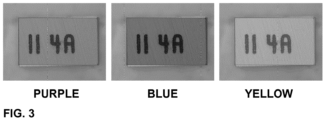
- Fig. 2 shows three different colour coded semiconducting wafers produced in accordance with the method set out in the preceding paragraphs. Each wafer comprises approximately 300 devices (i.e. 0402 sized). The colouring of a top surface of these wafers may be achieved by stacking multiple bi-layers of titanium oxide TiO 2 and aluminium oxide Al 2 O 3 using the ALD process.
- Fig. 3 shows conceptual views of three finished CSP products (1006 sized), each comprising one of the three wafer examples with colour coded markings shown in Fig. 2 .
- an insulating layer comprising Al 2 O 3 and TiO 2 with a thickness of 50nm may be employed.
- an insulating layer comprising Al 2 O 3 and TiO 2 with a thickness of 100nm may be employed.
- an insulating layer comprising Al 2 O 3 and TiO 2 with a thickness of 150nm may be employed.
- colour coded marking may also be applied to the CSP as a by-product during plasma dicing.
- Plasma dicing is a process used for cutting or singulating wafers, i.e. separation of wafers during fabrication.
- a common process for Plasma dicing is called “Bosch process”. This dry etching process creates a scalloped sidewall on a die, which may work as an optical grid by the formed grooves parallel to one of the two major surfaces called back side or front side. In dependency of the size of the grooves and the incident angle of the incident light, the surface appears coloured.
- Plasma dicing employs a dry etching process that makes use of fluorine chemistry. Unlike blade dicing, where contact is made between a blade and the wafer during cutting which may lead to the wafer chipping or cracking, no physical contact is made with plasma dicing. In addition, unlike blade dicing which require more blade processing time to perform more cut lines, the dicing process time for plasma dicing remains more or less the same regardless of the chip size. Plasma is therefore suited for cutting micro-sized chips of 500 ⁇ m square or smaller.
- a by-product of plasma dicing is the formation of multi-coloured strips on the semiconductor wafer surface during the singulating process. That is, walls of the CSP may appear multi coloured, because of some slight process variation and grooves/stripes.
- colour coded marking may be applied to the CSP device after completion of the fabrication of the CSP device or semiconductor wafer.
- an insulation material layer is applied to the outer packaging of the CSP device to encapsulate and protect the semiconductor die within the device.
- separate or additional fabrication process steps may be performed to apply colour coded marking on top of the insulation material.
- the colour coded marking may be a type of paint, a dye, etc.
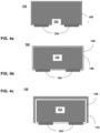
- Fig. 4a illustrates a semiconductor CSP 100 falling within the scope of the present invention, and comprising a semiconductor die 102 and a plurality of electrical contacts 104.
- the die 102 is encapsulated in an insulating layer 106, which is Al 2 O 3 , or a combination of Al 2 O 3 and TiO 2 .
- a colour of the insulating layer 106 is dependent upon the thickness of the Al 2 O 3 layers, or the sum of the thicknesses of Al 2 O 3 and TiO 2 layers (where both materials are present).
- Fig. 4b illustrates a semiconductor CSP 100 falling within the scope of the present invention only when the insulating layer is a layer of aluminium oxide or a stack of one or more bi-layers of aluminium oxide and titanium dioxide. Otherwise Fig. 4b is an example not forming part of the present invention but useful for understanding it.
- the semiconductor CSP 100 comprises a semiconductor die 102 and a plurality of electrical contacts 104.
- the die 102 is encapsulated in an insulating layer 106, which comprises an additive.
- the additive comprises a colouring additive that provides a colour component to the insulating layer 106.
- Fig. 4c illustrates a semiconductor CSP 100 falling within the scope of the present invention only when the insulating layer is a layer of aluminium oxide or a stack of one or more bi-layers of aluminium oxide and titanium dioxide. Otherwise Fig. 4c is an example not forming part of the present invention but useful for understanding it.
- the semiconductor CSP 100 comprises a semiconductor die 102 and a plurality of electrical contacts 104.
- the die 102 is encapsulated in an insulating layer 106, an outer surface of which is coated with a layer 108 containing an additive.
- the additive comprises a colouring additive that provides a colour component to the insulating layer 106.
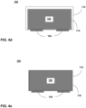
- Fig. 4d illustrates a semiconductor CSP 100 falling under the scope of the present invention only when the insulating layer is a layer of aluminium oxide or a stack of one or more bi-layers of aluminium oxide and titanium dioxide. Otherwise Fig. 4d is an example not forming part of the present invention but useful for understanding it.
- the semiconductor CSP 100 comprises a semiconductor die 102 and a plurality of electrical contacts 104.
- the die 102 is encapsulated in a layer 112 containing an additive.
- the additive comprises a colouring additive that provides a colour component to the layer 112.
- a transparent insulating layer 114 surrounds the layer 112 and allows the underlying layer 112 to be observed.
- Fig. 4e illustrates a semiconductor CSP 100 falling under the scope of the present invention only when the insulating layer is a layer of aluminium oxide or a stack of one or more bi-layers of aluminium oxide and titanium dioxide. Otherwise Fig. 4e is an example not forming part of the present invention but useful for understanding it.
- the semiconductor CSP 100 comprises a semiconductor die 102 and a plurality of electrical contacts 104.
- the die 102 is encapsulated in an insulating layer 116, which comprises surface formations 118 in an outer surface thereof. These surface formations provide a colour component.
- the surface formations 118 comprise optical lattices.
Landscapes
- Structures Or Materials For Encapsulating Or Coating Semiconductor Devices Or Solid State Devices (AREA)
Claims (11)
- Halbleiterchip-Gehäuse, umfassend:einen Halbleiter-Die (102), wobei der Halbleiter-Die Folgendes umfasst: eine erste Hauptoberfläche, die einer zweiten Hauptoberfläche gegenüberliegt; eine Vielzahl von Seitenwänden, die sich zwischen der ersten Hauptoberfläche und der zweiten Hauptoberfläche erstrecken;eine Vielzahl von elektrischen Kontakten (104), die auf der zweiten Hauptoberfläche des Halbleiter-Die (102) angeordnet sind; undeine Isolierschicht (106), die auf der Vielzahl von Seitenwänden und auf der ersten Hauptoberfläche angeordnet ist, wobei die Isolierschicht eine maschinenlesbare Kennung umfasst, durch die ein Halbleiterchip-Gehäuse-Typ durch eine Identifikationseinrichtung identifizierbar ist, welche die maschinenlesbare Kennung liest, wobei die maschinenlesbare Kennung eine Farbkomponente umfasst,wobei die Isolierschicht (106) eine Schicht aus Aluminiumoxid oder ein Stapel aus einer oder mehreren Doppelschichten aus Aluminiumoxid und Titandioxid ist, wobei die Isolierschicht (106) eine vorbestimmte Dicke aufweist, die so beschaffen ist, dass sie eine spezifische Farbe hat, die der Farbe der maschinenlesbaren Kennung entspricht.
- Halbleiterchip-Gehäuse nach Anspruch 1, wobei die Isolierschicht (106) eine Aluminiumoxidschicht mit einer Dicke von 5 nm, 10 nm, 15 nm, 20 nm, 25 nm, 30 nm, 35 nm, 40 nm, 45 nm, 50 nm, 55 nm, 60 nm, 65 nm, 70 nm, 75 nm, 80 nm, 85 nm, 90 nm, 95 nm, 100 nm, 105 nm, 110 nm, 115 nm, 120 nm, 125 nm, 130 nm, 135 nm, 140 nm, 145 nm, 150 nm, 155 nm, 160 nm, 165 nm, 170 nm, 175 nm, 180 nm, 185 nm, 190 nm, 195 nm, 200 nm, oder ein Stapel aus einer oder mehreren Doppelschichten aus Aluminiumoxid und Titandioxid mit einer Dicke von 50 nm, 100 nm oder 150 nm ist.
- Halbleiterchip-Gehäuse nach einem der vorstehenden Ansprüche, wobei
die Isolierschicht (106) als eine konforme Schicht auf dem Halbleiter-Die (102) durch Atomlagenabscheidung oder Niedertemperatur-PECVD gebildet wird. - Halbleiterchip-Gehäuse nach einem der Ansprüche 1 bis 3, wobei die Farbkomponente einen Zusatzstoff zu der Isolierschicht (106) umfasst.
- Halbleiterchip-Gehäuse nach Anspruch 4, wobei der Zusatzstoff einen Farbstoff oder eine Farbe umfasst.
- Halbleiterchip-Gehäuse nach einem der Ansprüche 1 bis 5, wobei die Farbkomponente einen Zusatzstoff umfasst, der in einer Schicht auf einer äußeren Oberfläche der Isolierschicht (106) angeordnet ist.
- Halbleiterchip-Gehäuse nach Anspruch 6, wobei der Zusatzstoff einen Farbstoff oder eine Farbe umfasst.
- Halbleiterchip-Gehäuse nach einem der Ansprüche 1 bis 5, wobei die Farbkomponente einen Zusatzstoff umfasst, der in einer Schicht auf einer inneren Oberfläche der Isolierschicht (106) angeordnet ist.
- Halbleiterchip-Gehäuse nach Anspruch 8, wobei der Zusatzstoff einen Farbstoff oder eine Farbe umfasst.
- Halbleiterchip-Gehäuse nach einem der Ansprüche 1 bis 2, wobei die Farbkomponente unter Verwendung von Oberflächenstrukturen gebildet wird, die in Oberflächen und/oder Seitenwänden des Die (102) gebildet sind.
- Halbleiterchip-Gehäuse nach Anspruch 10, wobei die Oberflächenstrukturen optische Gitter umfassen.
Priority Applications (4)
| Application Number | Priority Date | Filing Date | Title |
|---|---|---|---|
| EP18212913.0A EP3671832B1 (de) | 2018-12-17 | 2018-12-17 | Halbleiter-chip-scale-gehäuse |
| CN201911085909.0A CN111326483A (zh) | 2018-12-17 | 2019-11-08 | 半导体芯片级封装件和方法 |
| CN202411482778.0A CN119340311A (zh) | 2018-12-17 | 2019-11-08 | 半导体芯片级封装件和方法 |
| US16/715,593 US11355446B2 (en) | 2018-12-17 | 2019-12-16 | Semiconductor chip scale package and method |
Applications Claiming Priority (1)
| Application Number | Priority Date | Filing Date | Title |
|---|---|---|---|
| EP18212913.0A EP3671832B1 (de) | 2018-12-17 | 2018-12-17 | Halbleiter-chip-scale-gehäuse |
Publications (2)
| Publication Number | Publication Date |
|---|---|
| EP3671832A1 EP3671832A1 (de) | 2020-06-24 |
| EP3671832B1 true EP3671832B1 (de) | 2025-05-07 |
Family
ID=64755126
Family Applications (1)
| Application Number | Title | Priority Date | Filing Date |
|---|---|---|---|
| EP18212913.0A Active EP3671832B1 (de) | 2018-12-17 | 2018-12-17 | Halbleiter-chip-scale-gehäuse |
Country Status (3)
| Country | Link |
|---|---|
| US (1) | US11355446B2 (de) |
| EP (1) | EP3671832B1 (de) |
| CN (2) | CN111326483A (de) |
Families Citing this family (1)
| Publication number | Priority date | Publication date | Assignee | Title |
|---|---|---|---|---|
| CN119133152B (zh) * | 2024-09-11 | 2025-08-26 | 上海羲禾科技有限公司 | 芯片结构、芯片编码方法、芯片处理方法及程序产品 |
Family Cites Families (11)
| Publication number | Priority date | Publication date | Assignee | Title |
|---|---|---|---|---|
| SG106050A1 (en) * | 2000-03-13 | 2004-09-30 | Megic Corp | Method of manufacture and identification of semiconductor chip marked for identification with internal marking indicia and protection thereof by non-black layer and device produced thereby |
| TWI303870B (en) * | 2005-12-30 | 2008-12-01 | Advanced Semiconductor Eng | Structure and mtehod for packaging a chip |
| TWI396788B (zh) * | 2009-10-01 | 2013-05-21 | Taiwan Textile Res Inst | 彩色織物 |
| JP2012043953A (ja) * | 2010-08-18 | 2012-03-01 | Renesas Electronics Corp | 電子部品および電子部品の製造方法 |
| DE102012217539A1 (de) * | 2012-09-27 | 2014-05-15 | Osram Opto Semiconductors Gmbh | Optoelektronisches Bauteil und Verfahren zur Herstellung eines optoelektronischen Bauteils |
| US10020264B2 (en) * | 2015-04-28 | 2018-07-10 | Infineon Technologies Ag | Integrated circuit substrate and method for manufacturing the same |
| US20180073159A1 (en) * | 2016-09-09 | 2018-03-15 | Apple Inc. | Interference colored titanium with protective oxide film |
| EP3364450A1 (de) * | 2017-02-16 | 2018-08-22 | Nexperia B.V. | Paket in chipgrösse |
| JP2018160527A (ja) * | 2017-03-22 | 2018-10-11 | 東芝メモリ株式会社 | 半導体パッケージ、及び、半導体パッケージのマーキング方法 |
| KR102111045B1 (ko) * | 2017-10-31 | 2020-05-14 | 엘지디스플레이 주식회사 | 표시장치 |
| US20190229064A1 (en) * | 2018-01-24 | 2019-07-25 | Powertech Technology Inc. | Laser color marking method for a semiconductor package |
-
2018
- 2018-12-17 EP EP18212913.0A patent/EP3671832B1/de active Active
-
2019
- 2019-11-08 CN CN201911085909.0A patent/CN111326483A/zh active Pending
- 2019-11-08 CN CN202411482778.0A patent/CN119340311A/zh active Pending
- 2019-12-16 US US16/715,593 patent/US11355446B2/en active Active
Also Published As
| Publication number | Publication date |
|---|---|
| CN119340311A (zh) | 2025-01-21 |
| US20200194377A1 (en) | 2020-06-18 |
| EP3671832A1 (de) | 2020-06-24 |
| CN111326483A (zh) | 2020-06-23 |
| US11355446B2 (en) | 2022-06-07 |
Similar Documents
| Publication | Publication Date | Title |
|---|---|---|
| US11348833B2 (en) | IR assisted fan-out wafer level packaging using silicon handler | |
| US8314034B2 (en) | Feature size reduction | |
| US7223612B2 (en) | Alignment of MTJ stack to conductive lines in the absence of topography | |
| EP1164639B1 (de) | Ausrichtmarken zur Herstellung einer Halbleitervorrichtung | |
| US20190139767A1 (en) | Method for preparing a semiconductor structure | |
| US20190287901A1 (en) | Electrical fuse and/or resistor structures | |
| DE102019114212A1 (de) | Verfahren zum Herstellen einer Umverteilungsschaltkreisstruktur | |
| US6618149B1 (en) | Method of identifying film stacks based upon optical properties | |
| US11908885B2 (en) | Semiconductor device structure with magnetic element | |
| US20070013044A9 (en) | Packaged integrated circuits and methods of producing thereof | |
| US20080023802A1 (en) | Semiconductor device having a scribeline structure favorable for preventing chipping | |
| US10147611B1 (en) | Method for preparing semiconductor structures | |
| US10461038B1 (en) | Methods of alignment marking semiconductor wafers, and semiconductor packages having portions of alignment markings | |
| TWI697949B (zh) | 半導體裝置及其形成方法 | |
| CN116646338A (zh) | 半导体结构的制备方法 | |
| US11355446B2 (en) | Semiconductor chip scale package and method | |
| EP0129915B1 (de) | Verfahren zum Herstellen einer integrierten Schaltungsanordnung | |
| CN117637483A (zh) | 具有叠置标记的半导体结构、其制备方法及其制备系统 | |
| US11450616B2 (en) | Using a backside mask layer for forming a unique die mark identifier pattern | |
| DE102013109590A1 (de) | Verfahren zum Bearbeiten eines Wafers und Verfahren zum Zertrennen eines Wafers | |
| US9887134B2 (en) | Semiconductor devices, methods of manufacture thereof, and methods of singulating semiconductor devices | |
| JP2004363608A (ja) | 測定の信頼度を向上させられる測定用パターンを備える半導体装置及び測定用パターンを利用した半導体装置の測定方法 | |
| US6249036B1 (en) | Stepper alignment mark formation with dual field oxide process | |
| US7615475B2 (en) | Method for fabricating landing polysilicon contact structures for semiconductor devices | |
| US10157796B1 (en) | Forming of marking trenches in structure for multiple patterning lithography |
Legal Events
| Date | Code | Title | Description |
|---|---|---|---|
| PUAI | Public reference made under article 153(3) epc to a published international application that has entered the european phase |
Free format text: ORIGINAL CODE: 0009012 |
|
| STAA | Information on the status of an ep patent application or granted ep patent |
Free format text: STATUS: THE APPLICATION HAS BEEN PUBLISHED |
|
| AK | Designated contracting states |
Kind code of ref document: A1 Designated state(s): AL AT BE BG CH CY CZ DE DK EE ES FI FR GB GR HR HU IE IS IT LI LT LU LV MC MK MT NL NO PL PT RO RS SE SI SK SM TR |
|
| AX | Request for extension of the european patent |
Extension state: BA ME |
|
| STAA | Information on the status of an ep patent application or granted ep patent |
Free format text: STATUS: REQUEST FOR EXAMINATION WAS MADE |
|
| STAA | Information on the status of an ep patent application or granted ep patent |
Free format text: STATUS: EXAMINATION IS IN PROGRESS |
|
| 17P | Request for examination filed |
Effective date: 20201224 |
|
| RBV | Designated contracting states (corrected) |
Designated state(s): AL AT BE BG CH CY CZ DE DK EE ES FI FR GB GR HR HU IE IS IT LI LT LU LV MC MK MT NL NO PL PT RO RS SE SI SK SM TR |
|
| 17Q | First examination report despatched |
Effective date: 20210201 |
|
| GRAP | Despatch of communication of intention to grant a patent |
Free format text: ORIGINAL CODE: EPIDOSNIGR1 |
|
| STAA | Information on the status of an ep patent application or granted ep patent |
Free format text: STATUS: GRANT OF PATENT IS INTENDED |
|
| INTG | Intention to grant announced |
Effective date: 20241203 |
|
| RIN1 | Information on inventor provided before grant (corrected) |
Inventor name: FISCHER, JAN Inventor name: SPROGIES, TOBIAS |
|
| GRAS | Grant fee paid |
Free format text: ORIGINAL CODE: EPIDOSNIGR3 |
|
| GRAA | (expected) grant |
Free format text: ORIGINAL CODE: 0009210 |
|
| STAA | Information on the status of an ep patent application or granted ep patent |
Free format text: STATUS: THE PATENT HAS BEEN GRANTED |
|
| AK | Designated contracting states |
Kind code of ref document: B1 Designated state(s): AL AT BE BG CH CY CZ DE DK EE ES FI FR GB GR HR HU IE IS IT LI LT LU LV MC MK MT NL NO PL PT RO RS SE SI SK SM TR |
|
| REG | Reference to a national code |
Ref country code: GB Ref legal event code: FG4D |
|
| REG | Reference to a national code |
Ref country code: CH Ref legal event code: EP |
|
| REG | Reference to a national code |
Ref country code: DE Ref legal event code: R096 Ref document number: 602018081690 Country of ref document: DE |
|
| REG | Reference to a national code |
Ref country code: IE Ref legal event code: FG4D |
|
| REG | Reference to a national code |
Ref country code: NL Ref legal event code: MP Effective date: 20250507 |
|
| PG25 | Lapsed in a contracting state [announced via postgrant information from national office to epo] |
Ref country code: FI Free format text: LAPSE BECAUSE OF FAILURE TO SUBMIT A TRANSLATION OF THE DESCRIPTION OR TO PAY THE FEE WITHIN THE PRESCRIBED TIME-LIMIT Effective date: 20250507 Ref country code: ES Free format text: LAPSE BECAUSE OF FAILURE TO SUBMIT A TRANSLATION OF THE DESCRIPTION OR TO PAY THE FEE WITHIN THE PRESCRIBED TIME-LIMIT Effective date: 20250507 Ref country code: PT Free format text: LAPSE BECAUSE OF FAILURE TO SUBMIT A TRANSLATION OF THE DESCRIPTION OR TO PAY THE FEE WITHIN THE PRESCRIBED TIME-LIMIT Effective date: 20250908 |
|
| REG | Reference to a national code |
Ref country code: LT Ref legal event code: MG9D |
|
| PG25 | Lapsed in a contracting state [announced via postgrant information from national office to epo] |
Ref country code: NO Free format text: LAPSE BECAUSE OF FAILURE TO SUBMIT A TRANSLATION OF THE DESCRIPTION OR TO PAY THE FEE WITHIN THE PRESCRIBED TIME-LIMIT Effective date: 20250807 Ref country code: GR Free format text: LAPSE BECAUSE OF FAILURE TO SUBMIT A TRANSLATION OF THE DESCRIPTION OR TO PAY THE FEE WITHIN THE PRESCRIBED TIME-LIMIT Effective date: 20250808 |
|
| PG25 | Lapsed in a contracting state [announced via postgrant information from national office to epo] |
Ref country code: NL Free format text: LAPSE BECAUSE OF FAILURE TO SUBMIT A TRANSLATION OF THE DESCRIPTION OR TO PAY THE FEE WITHIN THE PRESCRIBED TIME-LIMIT Effective date: 20250507 Ref country code: PL Free format text: LAPSE BECAUSE OF FAILURE TO SUBMIT A TRANSLATION OF THE DESCRIPTION OR TO PAY THE FEE WITHIN THE PRESCRIBED TIME-LIMIT Effective date: 20250507 |
|
| REG | Reference to a national code |
Ref country code: AT Ref legal event code: MK05 Ref document number: 1793472 Country of ref document: AT Kind code of ref document: T Effective date: 20250507 |
|
| PG25 | Lapsed in a contracting state [announced via postgrant information from national office to epo] |
Ref country code: BG Free format text: LAPSE BECAUSE OF FAILURE TO SUBMIT A TRANSLATION OF THE DESCRIPTION OR TO PAY THE FEE WITHIN THE PRESCRIBED TIME-LIMIT Effective date: 20250507 |
|
| PG25 | Lapsed in a contracting state [announced via postgrant information from national office to epo] |
Ref country code: HR Free format text: LAPSE BECAUSE OF FAILURE TO SUBMIT A TRANSLATION OF THE DESCRIPTION OR TO PAY THE FEE WITHIN THE PRESCRIBED TIME-LIMIT Effective date: 20250507 |
|
| PG25 | Lapsed in a contracting state [announced via postgrant information from national office to epo] |
Ref country code: AT Free format text: LAPSE BECAUSE OF FAILURE TO SUBMIT A TRANSLATION OF THE DESCRIPTION OR TO PAY THE FEE WITHIN THE PRESCRIBED TIME-LIMIT Effective date: 20250507 |
|
| PG25 | Lapsed in a contracting state [announced via postgrant information from national office to epo] |
Ref country code: RS Free format text: LAPSE BECAUSE OF FAILURE TO SUBMIT A TRANSLATION OF THE DESCRIPTION OR TO PAY THE FEE WITHIN THE PRESCRIBED TIME-LIMIT Effective date: 20250807 |
|
| PG25 | Lapsed in a contracting state [announced via postgrant information from national office to epo] |
Ref country code: IS Free format text: LAPSE BECAUSE OF FAILURE TO SUBMIT A TRANSLATION OF THE DESCRIPTION OR TO PAY THE FEE WITHIN THE PRESCRIBED TIME-LIMIT Effective date: 20250907 |
|
| PG25 | Lapsed in a contracting state [announced via postgrant information from national office to epo] |
Ref country code: LV Free format text: LAPSE BECAUSE OF FAILURE TO SUBMIT A TRANSLATION OF THE DESCRIPTION OR TO PAY THE FEE WITHIN THE PRESCRIBED TIME-LIMIT Effective date: 20250507 |
|
| REG | Reference to a national code |
Ref country code: DE Ref legal event code: R079 Ref document number: 602018081690 Country of ref document: DE Free format text: PREVIOUS MAIN CLASS: H01L0023544000 Ipc: H10W0046000000 |
|
| PG25 | Lapsed in a contracting state [announced via postgrant information from national office to epo] |
Ref country code: SM Free format text: LAPSE BECAUSE OF FAILURE TO SUBMIT A TRANSLATION OF THE DESCRIPTION OR TO PAY THE FEE WITHIN THE PRESCRIBED TIME-LIMIT Effective date: 20250507 Ref country code: DK Free format text: LAPSE BECAUSE OF FAILURE TO SUBMIT A TRANSLATION OF THE DESCRIPTION OR TO PAY THE FEE WITHIN THE PRESCRIBED TIME-LIMIT Effective date: 20250507 |
|
| PG25 | Lapsed in a contracting state [announced via postgrant information from national office to epo] |
Ref country code: CZ Free format text: LAPSE BECAUSE OF FAILURE TO SUBMIT A TRANSLATION OF THE DESCRIPTION OR TO PAY THE FEE WITHIN THE PRESCRIBED TIME-LIMIT Effective date: 20250507 |
|
| PG25 | Lapsed in a contracting state [announced via postgrant information from national office to epo] |
Ref country code: EE Free format text: LAPSE BECAUSE OF FAILURE TO SUBMIT A TRANSLATION OF THE DESCRIPTION OR TO PAY THE FEE WITHIN THE PRESCRIBED TIME-LIMIT Effective date: 20250507 |
|
| PG25 | Lapsed in a contracting state [announced via postgrant information from national office to epo] |
Ref country code: RO Free format text: LAPSE BECAUSE OF FAILURE TO SUBMIT A TRANSLATION OF THE DESCRIPTION OR TO PAY THE FEE WITHIN THE PRESCRIBED TIME-LIMIT Effective date: 20250507 Ref country code: SK Free format text: LAPSE BECAUSE OF FAILURE TO SUBMIT A TRANSLATION OF THE DESCRIPTION OR TO PAY THE FEE WITHIN THE PRESCRIBED TIME-LIMIT Effective date: 20250507 |
|
| PG25 | Lapsed in a contracting state [announced via postgrant information from national office to epo] |
Ref country code: IT Free format text: LAPSE BECAUSE OF FAILURE TO SUBMIT A TRANSLATION OF THE DESCRIPTION OR TO PAY THE FEE WITHIN THE PRESCRIBED TIME-LIMIT Effective date: 20250507 |
|
| REG | Reference to a national code |
Ref country code: DE Ref legal event code: R097 Ref document number: 602018081690 Country of ref document: DE |
|
| PLBE | No opposition filed within time limit |
Free format text: ORIGINAL CODE: 0009261 |
|
| STAA | Information on the status of an ep patent application or granted ep patent |
Free format text: STATUS: NO OPPOSITION FILED WITHIN TIME LIMIT |
|
| REG | Reference to a national code |
Ref country code: CH Ref legal event code: L10 Free format text: ST27 STATUS EVENT CODE: U-0-0-L10-L00 (AS PROVIDED BY THE NATIONAL OFFICE) Effective date: 20260318 |
|
| PGFP | Annual fee paid to national office [announced via postgrant information from national office to epo] |
Ref country code: DE Payment date: 20251229 Year of fee payment: 8 |
|
| 26N | No opposition filed |
Effective date: 20260210 |
|
| PG25 | Lapsed in a contracting state [announced via postgrant information from national office to epo] |
Ref country code: LT Free format text: LAPSE BECAUSE OF FAILURE TO SUBMIT A TRANSLATION OF THE DESCRIPTION OR TO PAY THE FEE WITHIN THE PRESCRIBED TIME-LIMIT Effective date: 20250507 |
|
| PG25 | Lapsed in a contracting state [announced via postgrant information from national office to epo] |
Ref country code: MC Free format text: LAPSE BECAUSE OF FAILURE TO SUBMIT A TRANSLATION OF THE DESCRIPTION OR TO PAY THE FEE WITHIN THE PRESCRIBED TIME-LIMIT Effective date: 20250507 |
|
| REG | Reference to a national code |
Ref country code: CH Ref legal event code: H13 Free format text: ST27 STATUS EVENT CODE: U-0-0-H10-H13 (AS PROVIDED BY THE NATIONAL OFFICE) Effective date: 20260723 |
|
| PG25 | Lapsed in a contracting state [announced via postgrant information from national office to epo] |
Ref country code: SE Free format text: LAPSE BECAUSE OF FAILURE TO SUBMIT A TRANSLATION OF THE DESCRIPTION OR TO PAY THE FEE WITHIN THE PRESCRIBED TIME-LIMIT Effective date: 20250507 |