EP3671709A1 - Externe oled-kompensationsschaltung eines erschöpfungs-tft - Google Patents
Externe oled-kompensationsschaltung eines erschöpfungs-tft Download PDFInfo
- Publication number
- EP3671709A1 EP3671709A1 EP17921884.7A EP17921884A EP3671709A1 EP 3671709 A1 EP3671709 A1 EP 3671709A1 EP 17921884 A EP17921884 A EP 17921884A EP 3671709 A1 EP3671709 A1 EP 3671709A1
- Authority
- EP
- European Patent Office
- Prior art keywords
- thin film
- film transistor
- node
- compensation circuit
- reference potential
- Prior art date
- Legal status (The legal status is an assumption and is not a legal conclusion. Google has not performed a legal analysis and makes no representation as to the accuracy of the status listed.)
- Ceased
Links
Images



Classifications
-
- G—PHYSICS
- G09—EDUCATION; CRYPTOGRAPHY; DISPLAY; ADVERTISING; SEALS
- G09G—ARRANGEMENTS OR CIRCUITS FOR CONTROL OF INDICATING DEVICES USING STATIC MEANS TO PRESENT VARIABLE INFORMATION
- G09G3/00—Control arrangements or circuits, of interest only in connection with visual indicators other than cathode-ray tubes
- G09G3/20—Control arrangements or circuits, of interest only in connection with visual indicators other than cathode-ray tubes for presentation of an assembly of a number of characters, e.g. a page, by composing the assembly by combination of individual elements arranged in a matrix no fixed position being assigned to or needed to be assigned to the individual characters or partial characters
- G09G3/22—Control arrangements or circuits, of interest only in connection with visual indicators other than cathode-ray tubes for presentation of an assembly of a number of characters, e.g. a page, by composing the assembly by combination of individual elements arranged in a matrix no fixed position being assigned to or needed to be assigned to the individual characters or partial characters using controlled light sources
- G09G3/30—Control arrangements or circuits, of interest only in connection with visual indicators other than cathode-ray tubes for presentation of an assembly of a number of characters, e.g. a page, by composing the assembly by combination of individual elements arranged in a matrix no fixed position being assigned to or needed to be assigned to the individual characters or partial characters using controlled light sources using electroluminescent panels
- G09G3/32—Control arrangements or circuits, of interest only in connection with visual indicators other than cathode-ray tubes for presentation of an assembly of a number of characters, e.g. a page, by composing the assembly by combination of individual elements arranged in a matrix no fixed position being assigned to or needed to be assigned to the individual characters or partial characters using controlled light sources using electroluminescent panels semiconductive, e.g. using light-emitting diodes [LED]
- G09G3/3208—Control arrangements or circuits, of interest only in connection with visual indicators other than cathode-ray tubes for presentation of an assembly of a number of characters, e.g. a page, by composing the assembly by combination of individual elements arranged in a matrix no fixed position being assigned to or needed to be assigned to the individual characters or partial characters using controlled light sources using electroluminescent panels semiconductive, e.g. using light-emitting diodes [LED] organic, e.g. using organic light-emitting diodes [OLED]
- G09G3/3225—Control arrangements or circuits, of interest only in connection with visual indicators other than cathode-ray tubes for presentation of an assembly of a number of characters, e.g. a page, by composing the assembly by combination of individual elements arranged in a matrix no fixed position being assigned to or needed to be assigned to the individual characters or partial characters using controlled light sources using electroluminescent panels semiconductive, e.g. using light-emitting diodes [LED] organic, e.g. using organic light-emitting diodes [OLED] using an active matrix
- G09G3/3233—Control arrangements or circuits, of interest only in connection with visual indicators other than cathode-ray tubes for presentation of an assembly of a number of characters, e.g. a page, by composing the assembly by combination of individual elements arranged in a matrix no fixed position being assigned to or needed to be assigned to the individual characters or partial characters using controlled light sources using electroluminescent panels semiconductive, e.g. using light-emitting diodes [LED] organic, e.g. using organic light-emitting diodes [OLED] using an active matrix with pixel circuitry controlling the current through the light-emitting element
-
- G—PHYSICS
- G09—EDUCATION; CRYPTOGRAPHY; DISPLAY; ADVERTISING; SEALS
- G09G—ARRANGEMENTS OR CIRCUITS FOR CONTROL OF INDICATING DEVICES USING STATIC MEANS TO PRESENT VARIABLE INFORMATION
- G09G3/00—Control arrangements or circuits, of interest only in connection with visual indicators other than cathode-ray tubes
- G09G3/20—Control arrangements or circuits, of interest only in connection with visual indicators other than cathode-ray tubes for presentation of an assembly of a number of characters, e.g. a page, by composing the assembly by combination of individual elements arranged in a matrix no fixed position being assigned to or needed to be assigned to the individual characters or partial characters
- G09G3/22—Control arrangements or circuits, of interest only in connection with visual indicators other than cathode-ray tubes for presentation of an assembly of a number of characters, e.g. a page, by composing the assembly by combination of individual elements arranged in a matrix no fixed position being assigned to or needed to be assigned to the individual characters or partial characters using controlled light sources
- G09G3/30—Control arrangements or circuits, of interest only in connection with visual indicators other than cathode-ray tubes for presentation of an assembly of a number of characters, e.g. a page, by composing the assembly by combination of individual elements arranged in a matrix no fixed position being assigned to or needed to be assigned to the individual characters or partial characters using controlled light sources using electroluminescent panels
- G09G3/32—Control arrangements or circuits, of interest only in connection with visual indicators other than cathode-ray tubes for presentation of an assembly of a number of characters, e.g. a page, by composing the assembly by combination of individual elements arranged in a matrix no fixed position being assigned to or needed to be assigned to the individual characters or partial characters using controlled light sources using electroluminescent panels semiconductive, e.g. using light-emitting diodes [LED]
- G09G3/3208—Control arrangements or circuits, of interest only in connection with visual indicators other than cathode-ray tubes for presentation of an assembly of a number of characters, e.g. a page, by composing the assembly by combination of individual elements arranged in a matrix no fixed position being assigned to or needed to be assigned to the individual characters or partial characters using controlled light sources using electroluminescent panels semiconductive, e.g. using light-emitting diodes [LED] organic, e.g. using organic light-emitting diodes [OLED]
-
- G—PHYSICS
- G09—EDUCATION; CRYPTOGRAPHY; DISPLAY; ADVERTISING; SEALS
- G09G—ARRANGEMENTS OR CIRCUITS FOR CONTROL OF INDICATING DEVICES USING STATIC MEANS TO PRESENT VARIABLE INFORMATION
- G09G3/00—Control arrangements or circuits, of interest only in connection with visual indicators other than cathode-ray tubes
- G09G3/20—Control arrangements or circuits, of interest only in connection with visual indicators other than cathode-ray tubes for presentation of an assembly of a number of characters, e.g. a page, by composing the assembly by combination of individual elements arranged in a matrix no fixed position being assigned to or needed to be assigned to the individual characters or partial characters
- G09G3/22—Control arrangements or circuits, of interest only in connection with visual indicators other than cathode-ray tubes for presentation of an assembly of a number of characters, e.g. a page, by composing the assembly by combination of individual elements arranged in a matrix no fixed position being assigned to or needed to be assigned to the individual characters or partial characters using controlled light sources
- G09G3/30—Control arrangements or circuits, of interest only in connection with visual indicators other than cathode-ray tubes for presentation of an assembly of a number of characters, e.g. a page, by composing the assembly by combination of individual elements arranged in a matrix no fixed position being assigned to or needed to be assigned to the individual characters or partial characters using controlled light sources using electroluminescent panels
- G09G3/32—Control arrangements or circuits, of interest only in connection with visual indicators other than cathode-ray tubes for presentation of an assembly of a number of characters, e.g. a page, by composing the assembly by combination of individual elements arranged in a matrix no fixed position being assigned to or needed to be assigned to the individual characters or partial characters using controlled light sources using electroluminescent panels semiconductive, e.g. using light-emitting diodes [LED]
- G09G3/3208—Control arrangements or circuits, of interest only in connection with visual indicators other than cathode-ray tubes for presentation of an assembly of a number of characters, e.g. a page, by composing the assembly by combination of individual elements arranged in a matrix no fixed position being assigned to or needed to be assigned to the individual characters or partial characters using controlled light sources using electroluminescent panels semiconductive, e.g. using light-emitting diodes [LED] organic, e.g. using organic light-emitting diodes [OLED]
- G09G3/3225—Control arrangements or circuits, of interest only in connection with visual indicators other than cathode-ray tubes for presentation of an assembly of a number of characters, e.g. a page, by composing the assembly by combination of individual elements arranged in a matrix no fixed position being assigned to or needed to be assigned to the individual characters or partial characters using controlled light sources using electroluminescent panels semiconductive, e.g. using light-emitting diodes [LED] organic, e.g. using organic light-emitting diodes [OLED] using an active matrix
-
- G—PHYSICS
- G09—EDUCATION; CRYPTOGRAPHY; DISPLAY; ADVERTISING; SEALS
- G09G—ARRANGEMENTS OR CIRCUITS FOR CONTROL OF INDICATING DEVICES USING STATIC MEANS TO PRESENT VARIABLE INFORMATION
- G09G3/00—Control arrangements or circuits, of interest only in connection with visual indicators other than cathode-ray tubes
- G09G3/20—Control arrangements or circuits, of interest only in connection with visual indicators other than cathode-ray tubes for presentation of an assembly of a number of characters, e.g. a page, by composing the assembly by combination of individual elements arranged in a matrix no fixed position being assigned to or needed to be assigned to the individual characters or partial characters
- G09G3/22—Control arrangements or circuits, of interest only in connection with visual indicators other than cathode-ray tubes for presentation of an assembly of a number of characters, e.g. a page, by composing the assembly by combination of individual elements arranged in a matrix no fixed position being assigned to or needed to be assigned to the individual characters or partial characters using controlled light sources
- G09G3/30—Control arrangements or circuits, of interest only in connection with visual indicators other than cathode-ray tubes for presentation of an assembly of a number of characters, e.g. a page, by composing the assembly by combination of individual elements arranged in a matrix no fixed position being assigned to or needed to be assigned to the individual characters or partial characters using controlled light sources using electroluminescent panels
- G09G3/32—Control arrangements or circuits, of interest only in connection with visual indicators other than cathode-ray tubes for presentation of an assembly of a number of characters, e.g. a page, by composing the assembly by combination of individual elements arranged in a matrix no fixed position being assigned to or needed to be assigned to the individual characters or partial characters using controlled light sources using electroluminescent panels semiconductive, e.g. using light-emitting diodes [LED]
- G09G3/3208—Control arrangements or circuits, of interest only in connection with visual indicators other than cathode-ray tubes for presentation of an assembly of a number of characters, e.g. a page, by composing the assembly by combination of individual elements arranged in a matrix no fixed position being assigned to or needed to be assigned to the individual characters or partial characters using controlled light sources using electroluminescent panels semiconductive, e.g. using light-emitting diodes [LED] organic, e.g. using organic light-emitting diodes [OLED]
- G09G3/3225—Control arrangements or circuits, of interest only in connection with visual indicators other than cathode-ray tubes for presentation of an assembly of a number of characters, e.g. a page, by composing the assembly by combination of individual elements arranged in a matrix no fixed position being assigned to or needed to be assigned to the individual characters or partial characters using controlled light sources using electroluminescent panels semiconductive, e.g. using light-emitting diodes [LED] organic, e.g. using organic light-emitting diodes [OLED] using an active matrix
- G09G3/3258—Control arrangements or circuits, of interest only in connection with visual indicators other than cathode-ray tubes for presentation of an assembly of a number of characters, e.g. a page, by composing the assembly by combination of individual elements arranged in a matrix no fixed position being assigned to or needed to be assigned to the individual characters or partial characters using controlled light sources using electroluminescent panels semiconductive, e.g. using light-emitting diodes [LED] organic, e.g. using organic light-emitting diodes [OLED] using an active matrix with pixel circuitry controlling the voltage across the light-emitting element
-
- G—PHYSICS
- G09—EDUCATION; CRYPTOGRAPHY; DISPLAY; ADVERTISING; SEALS
- G09G—ARRANGEMENTS OR CIRCUITS FOR CONTROL OF INDICATING DEVICES USING STATIC MEANS TO PRESENT VARIABLE INFORMATION
- G09G3/00—Control arrangements or circuits, of interest only in connection with visual indicators other than cathode-ray tubes
- G09G3/20—Control arrangements or circuits, of interest only in connection with visual indicators other than cathode-ray tubes for presentation of an assembly of a number of characters, e.g. a page, by composing the assembly by combination of individual elements arranged in a matrix no fixed position being assigned to or needed to be assigned to the individual characters or partial characters
- G09G3/22—Control arrangements or circuits, of interest only in connection with visual indicators other than cathode-ray tubes for presentation of an assembly of a number of characters, e.g. a page, by composing the assembly by combination of individual elements arranged in a matrix no fixed position being assigned to or needed to be assigned to the individual characters or partial characters using controlled light sources
- G09G3/30—Control arrangements or circuits, of interest only in connection with visual indicators other than cathode-ray tubes for presentation of an assembly of a number of characters, e.g. a page, by composing the assembly by combination of individual elements arranged in a matrix no fixed position being assigned to or needed to be assigned to the individual characters or partial characters using controlled light sources using electroluminescent panels
- G09G3/32—Control arrangements or circuits, of interest only in connection with visual indicators other than cathode-ray tubes for presentation of an assembly of a number of characters, e.g. a page, by composing the assembly by combination of individual elements arranged in a matrix no fixed position being assigned to or needed to be assigned to the individual characters or partial characters using controlled light sources using electroluminescent panels semiconductive, e.g. using light-emitting diodes [LED]
- G09G3/3208—Control arrangements or circuits, of interest only in connection with visual indicators other than cathode-ray tubes for presentation of an assembly of a number of characters, e.g. a page, by composing the assembly by combination of individual elements arranged in a matrix no fixed position being assigned to or needed to be assigned to the individual characters or partial characters using controlled light sources using electroluminescent panels semiconductive, e.g. using light-emitting diodes [LED] organic, e.g. using organic light-emitting diodes [OLED]
- G09G3/3275—Details of drivers for data electrodes
- G09G3/3291—Details of drivers for data electrodes in which the data driver supplies a variable data voltage for setting the current through, or the voltage across, the light-emitting elements
-
- H—ELECTRICITY
- H10—SEMICONDUCTOR DEVICES; ELECTRIC SOLID-STATE DEVICES NOT OTHERWISE PROVIDED FOR
- H10D—INORGANIC ELECTRIC SEMICONDUCTOR DEVICES
- H10D86/00—Integrated devices formed in or on insulating or conducting substrates, e.g. formed in silicon-on-insulator [SOI] substrates or on stainless steel or glass substrates
- H10D86/40—Integrated devices formed in or on insulating or conducting substrates, e.g. formed in silicon-on-insulator [SOI] substrates or on stainless steel or glass substrates characterised by multiple TFTs
-
- H—ELECTRICITY
- H10—SEMICONDUCTOR DEVICES; ELECTRIC SOLID-STATE DEVICES NOT OTHERWISE PROVIDED FOR
- H10D—INORGANIC ELECTRIC SEMICONDUCTOR DEVICES
- H10D86/00—Integrated devices formed in or on insulating or conducting substrates, e.g. formed in silicon-on-insulator [SOI] substrates or on stainless steel or glass substrates
- H10D86/40—Integrated devices formed in or on insulating or conducting substrates, e.g. formed in silicon-on-insulator [SOI] substrates or on stainless steel or glass substrates characterised by multiple TFTs
- H10D86/441—Interconnections, e.g. scanning lines
-
- H—ELECTRICITY
- H10—SEMICONDUCTOR DEVICES; ELECTRIC SOLID-STATE DEVICES NOT OTHERWISE PROVIDED FOR
- H10K—ORGANIC ELECTRIC SOLID-STATE DEVICES
- H10K59/00—Integrated devices, or assemblies of multiple devices, comprising at least one organic light-emitting element covered by group H10K50/00
- H10K59/10—OLED displays
- H10K59/12—Active-matrix OLED [AMOLED] displays
- H10K59/121—Active-matrix OLED [AMOLED] displays characterised by the geometry or disposition of pixel elements
- H10K59/1213—Active-matrix OLED [AMOLED] displays characterised by the geometry or disposition of pixel elements the pixel elements being TFTs
-
- H—ELECTRICITY
- H10—SEMICONDUCTOR DEVICES; ELECTRIC SOLID-STATE DEVICES NOT OTHERWISE PROVIDED FOR
- H10K—ORGANIC ELECTRIC SOLID-STATE DEVICES
- H10K59/00—Integrated devices, or assemblies of multiple devices, comprising at least one organic light-emitting element covered by group H10K50/00
- H10K59/10—OLED displays
- H10K59/12—Active-matrix OLED [AMOLED] displays
- H10K59/131—Interconnections, e.g. wiring lines or terminals
-
- G—PHYSICS
- G09—EDUCATION; CRYPTOGRAPHY; DISPLAY; ADVERTISING; SEALS
- G09G—ARRANGEMENTS OR CIRCUITS FOR CONTROL OF INDICATING DEVICES USING STATIC MEANS TO PRESENT VARIABLE INFORMATION
- G09G2300/00—Aspects of the constitution of display devices
- G09G2300/04—Structural and physical details of display devices
- G09G2300/0404—Matrix technologies
- G09G2300/0417—Special arrangements specific to the use of low carrier mobility technology
-
- G—PHYSICS
- G09—EDUCATION; CRYPTOGRAPHY; DISPLAY; ADVERTISING; SEALS
- G09G—ARRANGEMENTS OR CIRCUITS FOR CONTROL OF INDICATING DEVICES USING STATIC MEANS TO PRESENT VARIABLE INFORMATION
- G09G2300/00—Aspects of the constitution of display devices
- G09G2300/04—Structural and physical details of display devices
- G09G2300/0421—Structural details of the set of electrodes
- G09G2300/0426—Layout of electrodes and connections
-
- G—PHYSICS
- G09—EDUCATION; CRYPTOGRAPHY; DISPLAY; ADVERTISING; SEALS
- G09G—ARRANGEMENTS OR CIRCUITS FOR CONTROL OF INDICATING DEVICES USING STATIC MEANS TO PRESENT VARIABLE INFORMATION
- G09G2300/00—Aspects of the constitution of display devices
- G09G2300/04—Structural and physical details of display devices
- G09G2300/0421—Structural details of the set of electrodes
- G09G2300/043—Compensation electrodes or other additional electrodes in matrix displays related to distortions or compensation signals, e.g. for modifying TFT threshold voltage in column driver
-
- G—PHYSICS
- G09—EDUCATION; CRYPTOGRAPHY; DISPLAY; ADVERTISING; SEALS
- G09G—ARRANGEMENTS OR CIRCUITS FOR CONTROL OF INDICATING DEVICES USING STATIC MEANS TO PRESENT VARIABLE INFORMATION
- G09G2300/00—Aspects of the constitution of display devices
- G09G2300/08—Active matrix structure, i.e. with use of active elements, inclusive of non-linear two terminal elements, in the pixels together with light emitting or modulating elements
- G09G2300/0809—Several active elements per pixel in active matrix panels
- G09G2300/0819—Several active elements per pixel in active matrix panels used for counteracting undesired variations, e.g. feedback or autozeroing
-
- G—PHYSICS
- G09—EDUCATION; CRYPTOGRAPHY; DISPLAY; ADVERTISING; SEALS
- G09G—ARRANGEMENTS OR CIRCUITS FOR CONTROL OF INDICATING DEVICES USING STATIC MEANS TO PRESENT VARIABLE INFORMATION
- G09G2300/00—Aspects of the constitution of display devices
- G09G2300/08—Active matrix structure, i.e. with use of active elements, inclusive of non-linear two terminal elements, in the pixels together with light emitting or modulating elements
- G09G2300/0809—Several active elements per pixel in active matrix panels
- G09G2300/0842—Several active elements per pixel in active matrix panels forming a memory circuit, e.g. a dynamic memory with one capacitor
-
- G—PHYSICS
- G09—EDUCATION; CRYPTOGRAPHY; DISPLAY; ADVERTISING; SEALS
- G09G—ARRANGEMENTS OR CIRCUITS FOR CONTROL OF INDICATING DEVICES USING STATIC MEANS TO PRESENT VARIABLE INFORMATION
- G09G2310/00—Command of the display device
- G09G2310/06—Details of flat display driving waveforms
- G09G2310/061—Details of flat display driving waveforms for resetting or blanking
-
- G—PHYSICS
- G09—EDUCATION; CRYPTOGRAPHY; DISPLAY; ADVERTISING; SEALS
- G09G—ARRANGEMENTS OR CIRCUITS FOR CONTROL OF INDICATING DEVICES USING STATIC MEANS TO PRESENT VARIABLE INFORMATION
- G09G2320/00—Control of display operating conditions
- G09G2320/04—Maintaining the quality of display appearance
- G09G2320/043—Preventing or counteracting the effects of ageing
- G09G2320/045—Compensation of drifts in the characteristics of light emitting or modulating elements
-
- H—ELECTRICITY
- H10—SEMICONDUCTOR DEVICES; ELECTRIC SOLID-STATE DEVICES NOT OTHERWISE PROVIDED FOR
- H10D—INORGANIC ELECTRIC SEMICONDUCTOR DEVICES
- H10D86/00—Integrated devices formed in or on insulating or conducting substrates, e.g. formed in silicon-on-insulator [SOI] substrates or on stainless steel or glass substrates
- H10D86/40—Integrated devices formed in or on insulating or conducting substrates, e.g. formed in silicon-on-insulator [SOI] substrates or on stainless steel or glass substrates characterised by multiple TFTs
- H10D86/60—Integrated devices formed in or on insulating or conducting substrates, e.g. formed in silicon-on-insulator [SOI] substrates or on stainless steel or glass substrates characterised by multiple TFTs wherein the TFTs are in active matrices
Definitions
- the present invention relates to the field of liquid crystal display, and more particularly to an OLED external compensation circuit of a depletion type TFT.
- OLED Organic light Emitting Display
- Fig. 1 is an illustrative diagram of a conventional 2T1C OLED driving circuit.
- the OLED is a current-driving drive, it inevitably affects the brightness of the OLED, which affects the normal display.
- one idea is to introduce an internal compensation circuit that counteracts the effect of the Vth shift.
- the conventional compensation circuit is more complex, the number of TFT is generally more than 5. So many TFTs will occupy a lot of space, and it will inevitably affect the pixel area of the opening area, which is not beneficial for high aperture and high-resolution display design.
- the IGZO (indium gallium zinc oxide)-TFT with BCE (Back-channel-etch) structure is the hotspot of the present research.
- the current performance of the IGZO-TFT is mostly as depletion type TFT, that is, the threshold voltage (Vth) is negative.
- the transfer characteristic curve of the depleted IGZO-TFT is shown in Fig. 2 , where the horizontal axis is the voltage (volts) and the vertical axis is the current (amperes). Due to the characteristics of the depleted IGZO-TFT, the circuit design is more complex.
- an object of the present invention to provide an OLED external compensation circuit for a depletion type TFT for the complicated characteristics of the conventional designs of the depletion type TFT and the OLED external compensation.
- the present invention provides an OLED external compensation circuit of a depletion type TFT, which comprises a first thin film transistor, a second thin film transistor, a capacitor, an organic light emitting diode, and a compensation circuit.
- the second thin film transistor is a depletion type.
- a gate electrode of the first thin film transistor is inputted with a gate line signal.
- a source electrode and a drain electrode of the first thin film transistor are respectively inputted with a data signal and connected with a first node.
- a gate of the second thin film transistor is connected with the first node.
- a source electrode and a drain electrode of the second thin film transistor are respectively inputted with a DC high voltage power supply and connected with a second node.
- Both ends of the capacitor are connected with at the first node and the second node.
- a positive electrode of the organic light emitting diode is connected with the second node and the negative electrode of the organic light emitting diode is grounded.
- the compensation circuit is connected with the first node and the second node.
- An AC reset signal is inputted to the compensation circuit.
- the AC reset signal is turned on at a blanking time of each frame when an OLED display device displays an image, and is turned off when normally operated on each frame.
- the compensation circuit changes the voltages of the first node and the second node.
- the compensation circuit comprises a third thin film transistor.
- a gate electrode of the third thin film transistor is inputted with the AC reset signal.
- a source electrode and a drain electrode of the third thin film transistor are respectively inputted with a DC reference potential and connected with the first node and the second node at the same time.
- the AC reset signal is at a high potential at which time the third thin film transistor is turned on and a signal of the DC reference potential is written to the first node and the second node.
- the gate line signal and the AC reset signal are at a low potential, the first thin film transistor and the third thin film transistor are turned off and the second thin film transistor is still turned on.
- the first thin film transistor is turned on and the data signal is written to the first node.
- the present invention further provides another OLED external compensation circuit of a depletion type TFT, which comprises a first thin film transistor, a second thin film transistor, a capacitor, an organic light emitting diode, and a compensation circuit.
- the second thin film transistor is a depletion type.
- a gate electrode of the first thin film transistor is inputted with a gate line signal.
- a source electrode and a drain electrode of the first thin film transistor are respectively inputted with a data signal and connected with a first node.
- a gate of the second thin film transistor is connected with the first node.
- a source electrode and a drain electrode of the second thin film transistor are respectively inputted with a DC high voltage power supply and connected with a second node. Both ends of the capacitor are connected with at the first node and the second node.
- a positive electrode of the organic light emitting diode is connected with the second node and the negative electrode of the organic light emitting diode is grounded.
- the compensation circuit is connected with the first node and the second node.
- An AC reference potential is inputted to the compensation circuit.
- the AC reference potential is turned on at a blanking time of each frame when an OLED display device displays an image, and is turned off when normally operated on each frame.
- the compensation circuit changes the voltages of the first node and the second node.
- the compensation circuit comprises a third thin film transistor and a fourth thin film transistor.
- a gate electrode of the third thin film transistor is inputted with the AC reference potential.
- a source electrode and a drain electrode of the third thin film transistor are respectively connected with a drain electrode/ source electrode of the fourth thin film transistor and connected with the first node and the second node at the same time.
- a gate electrode of the fourth thin film transistor is inputted with the AC reference potential.
- the AC reference potential is at a high potential at which time the third thin film transistor and the fourth thin film transistor are turned on and a signal of the AC reference potential is written to the first node and the second node.
- the gate line signal and the AC reference potential are at a low potential, the first thin film transistor, the third thin film transistor, and the fourth thin film transistor are turned off and the second thin film transistor is still turned on.
- the first thin film transistor is turned on and the data signal is written to the first node.
- the present invention further provides still another OLED external compensation circuit of a depletion type TFT, which comprises a first thin film transistor, a second thin film transistor, a capacitor, an organic light emitting diode, and a compensation circuit.
- the second thin film transistor is a depletion type.
- a gate electrode of the first thin film transistor is inputted with a gate line signal.
- a source electrode and a drain electrode of the first thin film transistor are respectively inputted with a data signal and connected with a first node.
- a gate of the second thin film transistor is connected with the first node.
- a source electrode and a drain electrode of the second thin film transistor are respectively inputted with a DC high voltage power supply and connected with a second node. Both ends of the capacitor are connected with at the first node and the second node.
- a positive electrode of the organic light emitting diode is connected with the second node and the negative electrode of the organic light emitting diode is grounded.
- the compensation circuit is connected with the first node and the second node.
- a first AC reference potential and a second AC reference potential are inputted to the compensation circuit.
- the first AC reference potential and the second AC reference potential are turned on at a blanking time of each frame when an OLED display device displays an image, and are turned off when normally operated on each frame. When the first AC reference potential and the second AC reference potential are turned on.
- the compensation circuit changes the voltages of the first node and the second node.
- the compensation circuit comprises a third thin film transistor and a fourth thin film transistor.
- a gate electrode of the third thin film transistor is inputted with the first AC reference potential.
- a source electrode and a drain electrode of the third thin film transistor are respectively inputted with the first AC reference potential and connected with the first node.
- a gate electrode of the fourth thin film transistor is inputted with the first AC reference potential.
- a source electrode and a drain electrode of the fourth thin film transistor are respectively inputted with the second AC reference potential and connected with the second node.
- the first AC reference potential and the second AC reference potential are at a high potential at which time the third thin film transistor and the fourth thin film transistor are turned on, a signal of the first AC reference potential is written to the first node and a signal of the second AC reference potential is written to the second node.
- the gate line signal and the first AC reference potential are at a low potential, the first thin film transistor, the third thin film transistor, and the fourth thin film transistor are turned off and the second thin film transistor is still turned on.
- the first thin film transistor is turned on and the data signal is written to the first node.
- the present invention provides an OLED external compensation circuit suitable for a depletion type TFT in view of the complicated characteristics of the conventional designs of the depletion type TFT and the OLED external compensation.
- the OLED external compensation circuit of another depletion type TFT of the present invention which reduces the cost of the system chip, thereby achieving cost reduction.
- the OLED external compensation circuit of another depletion type TFT of the present invention can be compatible with an enhanced TFT (Vth is positive) circuit.
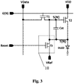
- Fig. 3 is a first external compensation circuit according to the present invention.
- the circuit is composed of three TFTs and one Cst, the main difference with the conventional external compensation circuit is the compensation circuit 10, which comprises a thin film transistor T3.
- a gate electrode of the thin film transistor is inputted with an AC reset signal Reset.
- a source electrode and a drain electrode of the thin film transistor are respectively inputted with a DC reference potential Vref and connected with the node S (N) and the node T (N) simultaneously.
- Vdata is the data signal.
- G (N) is the signal corresponding to any gate line.
- the high potential is 28V and the low potential is -7V VDD is a direct current (DC) high voltage power supply; the potential is generally set to be 28V Vref is the reference potential, which is less than the DC high voltage power supply of the VDD, the potential is generally set to 5V
- the Reset signal Reset is AC, the high potential is 28V and the low potential is -7V
- the depletion TFT of the present invention may be IGZO-TFT.
- Fig. 4 is a drawing of the corresponding waveform, which illustrate the correspondence between signals.
- STV is a trigger signal
- the time from the first STV to the second STV is used to define a frame time
- the STV signal of the OLED display device is introduced to help understand the operation of the compensation circuit.
- the reset signal Reset starts in the blanking time of each frame and closes when each frame normally works.
- the blanking time refers to the interval between the end of the n-th frame image signal and the start of the (n+ 1)th frame image signal of the OLED display device.
- the first stage is a first stage
- Fig. 5 is a second external compensation circuit according to the present invention.
- the circuit is composed of four TFTs and one Cst.
- the compensation circuit 20 includes a thin film transistor T3 and a thin film transistor T4.
- a gate electrode of T3 is inputted with the AC reference potential Vref
- a source electrode and a drain electrode of T3 are connected with a source/drain electrode of the T4, the node S (N) and the node T N) at the same time.
- a gate electrode of T4 is inputted with the AC reference potential Vref and the other source / drain electrodes of T4 are also inputted with the AC reference potential Vref
- Vdata is the data signal.
- G (N) is the signal corresponding to any gate line.
- the high potential is 28V and the low potential is -7V VDD is a direct current (DC) high voltage power supply, the potential is generally set to be 28V Vref is the reference potential, which is an AC power supply, the high potential is 28V and the low potential is -7V
- Fig. 6 is a drawing of the corresponding waveform, which illustrate the correspondence between signals.
- STV is a trigger signal
- the time from the first STV to the second STV is used to define a frame time.
- the Vref starts in the blanking time of each frame and closes when each frame normally works.
- the second circuit Compared with the first external compensation circuit, the second circuit increases with a TFT and increases the space, but eliminates the need for a Reset signal, reducing the cost of the integrated chip (IC), in order to achieve cost reduction.
- the first stage is a first stage
- Vref Blanking time phase, at this stage, Vref is at the high potential, then T3 and T4 are opened, signal of Vref is written to S (N) and T (N), potential of sides of the gate electrode and the source electrode of the TFT T2 are rewritten to the potential of Vref, and all the TFTs are homered.
- Fig. 7 is a third external compensation circuit according to the present invention.
- the circuit is composed of four TFTs and one Cst.
- the compensation circuit 30 includes thin film transistors T3, T4.
- a gate electrode of T3 is inputted with the AC reference potential Vrefl
- a source electrode and a drain electrode of T3 are respectively inputted with the AC reference potential Vref and connected with the node S (N).
- a gate electrode of T4 is inputted with the AC reference potential Vrefl.
- a source electrode and a drain electrode of T4 are respectively also inputted with the AC reference potential Vref2 and connected with the node T(N).
- Vdata is the data signal.
- G (N) is the signal corresponding to any gate line.
- the high potential is 28V and the low potential is -7V VDD is a direct current (DC) high voltage power supply; the potential is generally set to be 28V Vrefl and Vref2 are both the reference potential, which is an AC power supply, the high potential is 28V and the low potential is -7V
- the voltage difference between Vrefl and Vref2 is adjustable.
- Fig. 8 is a drawing of the corresponding waveform, which illustrate the correspondence between signals.
- STV is a trigger signal, and the time from the first STV to the second STV is used to define a frame time.
- the Vref starts in the blanking time of each frame and closes when each frame normally works.
- Vrefl the voltage difference between Vrefl and Vref2 is adjustable.
- the circuit can be compatible with enhanced TFT (Vth is positive) circuit.
- the first stage is a first stage
- Vref1 and Vref2 are at the high potential, then T3 and T4 are opened, signal of Vrefl is written to T (N), in other words, potential of sides of the gate electrode and the source electrode of the TFT T2 are respectively rewritten to the potentials of Vrefl and Verf2, and all the TFTs are homered.
- Vth>0, Vgs Vref1-Vref2 can be set to be greater than or equal to 0 and greater than Vth.
- Vth compensation phase When G (N) is on and T1 is on, the signal Vdata of data is written to node S (N).
- the present invention provides an OLED external compensation circuit suitable for a depletion type TFT in view of the complicated characteristics of the conventional designs of the depletion type TFT and the OLED external compensation.
- the OLED external compensation circuit of another depletion type TFT of the present invention which reduces the cost of the system chip, thereby achieving cost reduction.
- the OLED external compensation circuit of another depletion type TFT of the present invention can be compatible with an enhanced TFT (Vth is positive) circuit.
Landscapes
- Engineering & Computer Science (AREA)
- Physics & Mathematics (AREA)
- Computer Hardware Design (AREA)
- General Physics & Mathematics (AREA)
- Theoretical Computer Science (AREA)
- Microelectronics & Electronic Packaging (AREA)
- Geometry (AREA)
- Electroluminescent Light Sources (AREA)
- Control Of El Displays (AREA)
- Control Of Indicators Other Than Cathode Ray Tubes (AREA)
Priority Applications (1)
| Application Number | Priority Date | Filing Date | Title |
|---|---|---|---|
| EP25179909.4A EP4607497A3 (de) | 2017-08-14 | 2017-09-15 | Externe oled-kompensationsschaltung eines erschöpfungs-tft |
Applications Claiming Priority (2)
| Application Number | Priority Date | Filing Date | Title |
|---|---|---|---|
| CN201710693609.5A CN107393466B (zh) | 2017-08-14 | 2017-08-14 | 耗尽型tft的oled外部补偿电路 |
| PCT/CN2017/101976 WO2019033494A1 (zh) | 2017-08-14 | 2017-09-15 | 耗尽型tft的oled外部补偿电路 |
Related Child Applications (1)
| Application Number | Title | Priority Date | Filing Date |
|---|---|---|---|
| EP25179909.4A Division EP4607497A3 (de) | 2017-08-14 | 2017-09-15 | Externe oled-kompensationsschaltung eines erschöpfungs-tft |
Publications (2)
| Publication Number | Publication Date |
|---|---|
| EP3671709A1 true EP3671709A1 (de) | 2020-06-24 |
| EP3671709A4 EP3671709A4 (de) | 2021-05-12 |
Family
ID=60355671
Family Applications (2)
| Application Number | Title | Priority Date | Filing Date |
|---|---|---|---|
| EP17921884.7A Ceased EP3671709A4 (de) | 2017-08-14 | 2017-09-15 | Externe oled-kompensationsschaltung eines erschöpfungs-tft |
| EP25179909.4A Pending EP4607497A3 (de) | 2017-08-14 | 2017-09-15 | Externe oled-kompensationsschaltung eines erschöpfungs-tft |
Family Applications After (1)
| Application Number | Title | Priority Date | Filing Date |
|---|---|---|---|
| EP25179909.4A Pending EP4607497A3 (de) | 2017-08-14 | 2017-09-15 | Externe oled-kompensationsschaltung eines erschöpfungs-tft |
Country Status (6)
| Country | Link |
|---|---|
| US (2) | US10522078B2 (de) |
| EP (2) | EP3671709A4 (de) |
| JP (1) | JP6853411B2 (de) |
| KR (1) | KR20200036932A (de) |
| CN (1) | CN107393466B (de) |
| WO (1) | WO2019033494A1 (de) |
Families Citing this family (6)
| Publication number | Priority date | Publication date | Assignee | Title |
|---|---|---|---|---|
| CN107919091B (zh) * | 2018-01-03 | 2019-11-22 | 京东方科技集团股份有限公司 | 一种oled像素驱动电路及驱动方法、oled显示装置 |
| KR102710488B1 (ko) * | 2019-12-31 | 2024-09-25 | 엘지디스플레이 주식회사 | 유기발광 표시장치와 그 구동방법 |
| WO2022019664A1 (ko) * | 2020-07-21 | 2022-01-27 | 주식회사 엘지에너지솔루션 | 병렬 멀티 팩 모듈의 출력 제어 장치 및 방법 |
| CN111951731B (zh) * | 2020-08-21 | 2021-12-21 | 京东方科技集团股份有限公司 | 像素单元阵列及其驱动方法、显示面板和显示装置 |
| KR102763606B1 (ko) * | 2020-12-24 | 2025-02-05 | 엘지디스플레이 주식회사 | 듀얼 데이터배선을 포함하는 표시장치 |
| CN118379961B (zh) * | 2024-05-24 | 2024-10-15 | 国鲸合创(青岛)科技有限公司 | 主动式有机发光显示外部补偿电路及方法 |
Family Cites Families (32)
| Publication number | Priority date | Publication date | Assignee | Title |
|---|---|---|---|---|
| JP2007316454A (ja) * | 2006-05-29 | 2007-12-06 | Sony Corp | 画像表示装置 |
| JP2010181788A (ja) * | 2009-02-09 | 2010-08-19 | Sony Corp | 表示装置及びその駆動方法 |
| KR101351416B1 (ko) * | 2010-05-18 | 2014-01-14 | 엘지디스플레이 주식회사 | 액티브 매트릭스 유기 발광 다이오드 표시 장치의 전압 보상형 화소 회로 |
| JP2012237919A (ja) * | 2011-05-13 | 2012-12-06 | Sony Corp | 画素回路、表示装置、電子機器、及び、画素回路の駆動方法 |
| KR101528961B1 (ko) * | 2012-08-30 | 2015-06-16 | 엘지디스플레이 주식회사 | 유기발광 표시장치 및 그 구동방법 |
| US8946994B2 (en) * | 2012-09-25 | 2015-02-03 | Lg Display Co., Ltd. | Organic light emitting display device and driving method thereof |
| CN102930822B (zh) * | 2012-11-12 | 2014-12-24 | 京东方科技集团股份有限公司 | 像素电路、显示装置和像素电路的驱动方法 |
| CN102982767B (zh) * | 2012-12-10 | 2015-02-25 | 京东方科技集团股份有限公司 | 一种像素单元驱动电路、驱动方法及显示装置 |
| CN103915057A (zh) * | 2013-01-04 | 2014-07-09 | 友达光电股份有限公司 | 像素驱动电路及使用其的有机发光显示器 |
| CN103927969B (zh) * | 2013-06-28 | 2016-06-22 | 上海天马微电子有限公司 | 一种像素补偿电路及显示器 |
| CN103440843B (zh) * | 2013-08-07 | 2016-10-19 | 京东方科技集团股份有限公司 | 一种抑制老化的oled交流驱动电路、驱动方法及显示装置 |
| US9852687B2 (en) * | 2013-09-04 | 2017-12-26 | Joled Inc. | Display device and driving method |
| KR101702429B1 (ko) * | 2013-12-13 | 2017-02-03 | 엘지디스플레이 주식회사 | 보상 화소 구조를 갖는 유기발광표시장치 |
| KR102068589B1 (ko) * | 2013-12-30 | 2020-01-21 | 엘지디스플레이 주식회사 | 유기 발광 표시 장치 및 그의 구동 방법 |
| CN103700347B (zh) * | 2014-01-10 | 2015-11-04 | 深圳市华星光电技术有限公司 | 有机发光二极管的驱动电路 |
| CN104867441B (zh) | 2014-02-20 | 2017-07-28 | 北京大学深圳研究生院 | 一种像素电路、显示装置及显示驱动方法 |
| CN104103238B (zh) * | 2014-06-17 | 2016-04-06 | 京东方科技集团股份有限公司 | 一种像素电路及其驱动方法、显示装置 |
| CN104464616B (zh) * | 2014-10-28 | 2017-10-03 | 上海天马有机发光显示技术有限公司 | 像素电路及其驱动方法、显示面板 |
| KR102324865B1 (ko) * | 2014-12-29 | 2021-11-12 | 엘지디스플레이 주식회사 | 유기발광 표시장치와 그의 휘도 제어 방법 |
| CN104680982B (zh) * | 2015-03-27 | 2017-03-08 | 深圳市华星光电技术有限公司 | Amoled像素驱动电路及像素驱动方法 |
| KR102387392B1 (ko) * | 2015-06-26 | 2022-04-19 | 삼성디스플레이 주식회사 | 화소, 화소의 구동방법 및 화소를 포함하는 유기발광 표시장치 |
| KR102524459B1 (ko) * | 2015-08-27 | 2023-04-25 | 삼성디스플레이 주식회사 | 화소 및 그의 구동방법 |
| JP2017068032A (ja) * | 2015-09-30 | 2017-04-06 | ソニー株式会社 | 表示素子の駆動方法、表示装置、及び、電子機器 |
| KR102426457B1 (ko) * | 2016-02-29 | 2022-07-29 | 삼성디스플레이 주식회사 | 화소 및 이를 포함하는 유기 발광 표시 장치 |
| CN106205495A (zh) * | 2016-09-09 | 2016-12-07 | 深圳市华星光电技术有限公司 | Amoled像素驱动电路及像素驱动方法 |
| CN106328061B (zh) * | 2016-10-14 | 2019-03-12 | 深圳市华星光电技术有限公司 | Oled像素混合补偿电路及混合补偿方法 |
| CN106504703B (zh) * | 2016-10-18 | 2019-05-31 | 深圳市华星光电技术有限公司 | Amoled像素驱动电路及驱动方法 |
| KR102563968B1 (ko) * | 2016-11-21 | 2023-08-04 | 엘지디스플레이 주식회사 | 표시 장치 |
| CN108305587A (zh) * | 2017-01-11 | 2018-07-20 | 群创光电股份有限公司 | 显示装置 |
| CN106548753B (zh) * | 2017-01-20 | 2018-06-01 | 深圳市华星光电技术有限公司 | Amoled像素驱动系统及amoled像素驱动方法 |
| CN106782340B (zh) * | 2017-03-16 | 2018-09-07 | 深圳市华星光电技术有限公司 | 一种像素驱动电路及oled显示装置 |
| US10672338B2 (en) * | 2017-03-24 | 2020-06-02 | Apple Inc. | Organic light-emitting diode display with external compensation and anode reset |
-
2017
- 2017-08-14 CN CN201710693609.5A patent/CN107393466B/zh active Active
- 2017-09-15 EP EP17921884.7A patent/EP3671709A4/de not_active Ceased
- 2017-09-15 JP JP2020506164A patent/JP6853411B2/ja active Active
- 2017-09-15 WO PCT/CN2017/101976 patent/WO2019033494A1/zh not_active Ceased
- 2017-09-15 EP EP25179909.4A patent/EP4607497A3/de active Pending
- 2017-09-15 KR KR1020207007043A patent/KR20200036932A/ko not_active Ceased
- 2017-09-15 US US15/574,837 patent/US10522078B2/en not_active Expired - Fee Related
-
2019
- 2019-11-21 US US16/691,537 patent/US10854138B2/en active Active
Also Published As
| Publication number | Publication date |
|---|---|
| KR20200036932A (ko) | 2020-04-07 |
| JP2020529632A (ja) | 2020-10-08 |
| CN107393466B (zh) | 2019-01-15 |
| WO2019033494A1 (zh) | 2019-02-21 |
| US20200090585A1 (en) | 2020-03-19 |
| US10522078B2 (en) | 2019-12-31 |
| JP6853411B2 (ja) | 2021-03-31 |
| EP4607497A2 (de) | 2025-08-27 |
| US20190051252A1 (en) | 2019-02-14 |
| US10854138B2 (en) | 2020-12-01 |
| EP3671709A4 (de) | 2021-05-12 |
| CN107393466A (zh) | 2017-11-24 |
| EP4607497A3 (de) | 2025-10-15 |
Similar Documents
| Publication | Publication Date | Title |
|---|---|---|
| US10854138B2 (en) | OLED external compensation circuit of a depletion type TFT | |
| US10720104B2 (en) | Pixel circuit, display device and driving method for pixel circuit | |
| US10347177B2 (en) | Pixel driving circuit for avoiding flicker of light-emitting unit, driving method thereof, and display device | |
| US10157571B2 (en) | Display panel, method for driving the same and display device | |
| US10453390B2 (en) | Pixel circuit and method for driving the same | |
| CN106504703B (zh) | Amoled像素驱动电路及驱动方法 | |
| US20210327347A1 (en) | Pixel circuit and driving method thereof, and display panel | |
| US10032415B2 (en) | Pixel circuit and driving method thereof, display device | |
| EP3843071A1 (de) | Pixeleinheit, anzeigetafel und elektronische vorrichtung | |
| US11127342B2 (en) | Pixel circuit for driving light emitting diode to emit light and method of controlling the pixel circuit | |
| EP3654324A1 (de) | Amoled-pixeltreiberschaltung und pixelansteuerungsverfahren | |
| US9449554B2 (en) | Pixel driving circuit and driving method thereof, display apparatus | |
| CN112233621B (zh) | 一种像素驱动电路、显示面板及电子设备 | |
| WO2016011711A1 (zh) | 像素电路、像素电路的驱动方法和显示装置 | |
| US10347658B2 (en) | Pixel driving circuit and OLED display device that effectively compensate for threshold voltage imposed on a driving TFT | |
| EP3654325A1 (de) | Amoled-pixeltreiberschaltung und pixelansteuerungsverfahren | |
| US10204561B2 (en) | Amoled pixel driving circuit and pixel driving method | |
| CN113593473B (zh) | 一种显示面板驱动电路及驱动方法 | |
| WO2019090907A1 (zh) | 一种像素驱动电路及有机发光二极管显示装置 | |
| US20190333446A1 (en) | Pixel driving circuit and driving method thereof display panel and display apparatus | |
| CN115035852B (zh) | 像素驱动电路、显示面板及电子设备 | |
| US11308878B2 (en) | Pixel driving circuit and driving method thereof, display panel | |
| US20190066586A1 (en) | Pixel driver circuit and driving method thereof |
Legal Events
| Date | Code | Title | Description |
|---|---|---|---|
| STAA | Information on the status of an ep patent application or granted ep patent |
Free format text: STATUS: THE INTERNATIONAL PUBLICATION HAS BEEN MADE |
|
| PUAI | Public reference made under article 153(3) epc to a published international application that has entered the european phase |
Free format text: ORIGINAL CODE: 0009012 |
|
| STAA | Information on the status of an ep patent application or granted ep patent |
Free format text: STATUS: REQUEST FOR EXAMINATION WAS MADE |
|
| 17P | Request for examination filed |
Effective date: 20200310 |
|
| AK | Designated contracting states |
Kind code of ref document: A1 Designated state(s): AL AT BE BG CH CY CZ DE DK EE ES FI FR GB GR HR HU IE IS IT LI LT LU LV MC MK MT NL NO PL PT RO RS SE SI SK SM TR |
|
| AX | Request for extension of the european patent |
Extension state: BA ME |
|
| DAV | Request for validation of the european patent (deleted) | ||
| DAX | Request for extension of the european patent (deleted) | ||
| A4 | Supplementary search report drawn up and despatched |
Effective date: 20210414 |
|
| RIC1 | Information provided on ipc code assigned before grant |
Ipc: G09G 3/3208 20160101AFI20210408BHEP |
|
| STAA | Information on the status of an ep patent application or granted ep patent |
Free format text: STATUS: EXAMINATION IS IN PROGRESS |
|
| 17Q | First examination report despatched |
Effective date: 20221220 |
|
| REG | Reference to a national code |
Ref country code: DE Ref legal event code: R003 |
|
| STAA | Information on the status of an ep patent application or granted ep patent |
Free format text: STATUS: THE APPLICATION HAS BEEN REFUSED |
|
| 18R | Application refused |
Effective date: 20250324 |