EP3671310A1 - Optical manipulation apparatus for trapping or moving micro or nanoparticles - Google Patents
Optical manipulation apparatus for trapping or moving micro or nanoparticles Download PDFInfo
- Publication number
- EP3671310A1 EP3671310A1 EP18213584.8A EP18213584A EP3671310A1 EP 3671310 A1 EP3671310 A1 EP 3671310A1 EP 18213584 A EP18213584 A EP 18213584A EP 3671310 A1 EP3671310 A1 EP 3671310A1
- Authority
- EP
- European Patent Office
- Prior art keywords
- jet
- electromagnetic wave
- axis
- beams
- manipulation apparatus
- Prior art date
- Legal status (The legal status is an assumption and is not a legal conclusion. Google has not performed a legal analysis and makes no representation as to the accuracy of the status listed.)
- Withdrawn
Links
- 230000003287 optical effect Effects 0.000 title claims abstract description 40
- 239000002105 nanoparticle Substances 0.000 title claims abstract description 22
- 239000011859 microparticle Substances 0.000 title claims abstract description 20
- 238000005286 illumination Methods 0.000 claims description 44
- 239000000463 material Substances 0.000 claims description 33
- 230000005855 radiation Effects 0.000 claims description 20
- NCGICGYLBXGBGN-UHFFFAOYSA-N 3-morpholin-4-yl-1-oxa-3-azonia-2-azanidacyclopent-3-en-5-imine;hydrochloride Chemical compound Cl.[N-]1OC(=N)C=[N+]1N1CCOCC1 NCGICGYLBXGBGN-UHFFFAOYSA-N 0.000 claims description 7
- 239000011521 glass Substances 0.000 claims description 7
- 101100420681 Caenorhabditis elegans tir-1 gene Proteins 0.000 claims description 6
- 239000002861 polymer material Substances 0.000 claims description 3
- 238000001228 spectrum Methods 0.000 claims description 3
- 101100259716 Arabidopsis thaliana TAA1 gene Proteins 0.000 claims description 2
- 101100206899 Saccharomyces cerevisiae (strain ATCC 204508 / S288c) TIR2 gene Proteins 0.000 claims description 2
- 101150044379 TIR1 gene Proteins 0.000 claims description 2
- 238000009826 distribution Methods 0.000 description 27
- 239000002245 particle Substances 0.000 description 15
- 238000004088 simulation Methods 0.000 description 10
- 230000005672 electromagnetic field Effects 0.000 description 7
- 239000006185 dispersion Substances 0.000 description 6
- 230000000694 effects Effects 0.000 description 4
- 238000012576 optical tweezer Methods 0.000 description 3
- 230000008901 benefit Effects 0.000 description 2
- PCHJSUWPFVWCPO-UHFFFAOYSA-N gold Chemical compound [Au] PCHJSUWPFVWCPO-UHFFFAOYSA-N 0.000 description 2
- 239000010931 gold Substances 0.000 description 2
- 229910052737 gold Inorganic materials 0.000 description 2
- 239000002184 metal Substances 0.000 description 2
- 229910052751 metal Inorganic materials 0.000 description 2
- 238000000034 method Methods 0.000 description 2
- 150000004767 nitrides Chemical class 0.000 description 2
- 230000015572 biosynthetic process Effects 0.000 description 1
- 239000004020 conductor Substances 0.000 description 1
- 230000003247 decreasing effect Effects 0.000 description 1
- 239000003989 dielectric material Substances 0.000 description 1
- 239000003814 drug Substances 0.000 description 1
- 230000014509 gene expression Effects 0.000 description 1
- 230000003993 interaction Effects 0.000 description 1
- 230000007935 neutral effect Effects 0.000 description 1
Images


Classifications
-
- B—PERFORMING OPERATIONS; TRANSPORTING
- B25—HAND TOOLS; PORTABLE POWER-DRIVEN TOOLS; MANIPULATORS
- B25J—MANIPULATORS; CHAMBERS PROVIDED WITH MANIPULATION DEVICES
- B25J7/00—Micromanipulators
-
- G—PHYSICS
- G02—OPTICS
- G02B—OPTICAL ELEMENTS, SYSTEMS OR APPARATUS
- G02B21/00—Microscopes
- G02B21/32—Micromanipulators structurally combined with microscopes
-
- G—PHYSICS
- G02—OPTICS
- G02B—OPTICAL ELEMENTS, SYSTEMS OR APPARATUS
- G02B27/00—Optical systems or apparatus not provided for by any of the groups G02B1/00 - G02B26/00, G02B30/00
- G02B27/56—Optics using evanescent waves, i.e. inhomogeneous waves
-
- G—PHYSICS
- G02—OPTICS
- G02B—OPTICAL ELEMENTS, SYSTEMS OR APPARATUS
- G02B3/00—Simple or compound lenses
- G02B3/0006—Arrays
- G02B3/0037—Arrays characterized by the distribution or form of lenses
- G02B3/0043—Inhomogeneous or irregular arrays, e.g. varying shape, size, height
-
- G—PHYSICS
- G02—OPTICS
- G02F—OPTICAL DEVICES OR ARRANGEMENTS FOR THE CONTROL OF LIGHT BY MODIFICATION OF THE OPTICAL PROPERTIES OF THE MEDIA OF THE ELEMENTS INVOLVED THEREIN; NON-LINEAR OPTICS; FREQUENCY-CHANGING OF LIGHT; OPTICAL LOGIC ELEMENTS; OPTICAL ANALOGUE/DIGITAL CONVERTERS
- G02F1/00—Devices or arrangements for the control of the intensity, colour, phase, polarisation or direction of light arriving from an independent light source, e.g. switching, gating or modulating; Non-linear optics
- G02F1/29—Devices or arrangements for the control of the intensity, colour, phase, polarisation or direction of light arriving from an independent light source, e.g. switching, gating or modulating; Non-linear optics for the control of the position or the direction of light beams, i.e. deflection
Definitions
- the present disclosure relates to the field of optics and photonics, and more specifically to an optical manipulation device for trapping or moving micro or nanoparticles.
- the disclosure can be of interest in any field where neutral particles have to be trapped and/or manipulated as for instance in atomic physic, nonlinear physics, biology and medicine, etc.
- nanojets photonic condensed optical beams, or photonic "nanojets"
- the structured field of nanojets may induce specific optical forces providing the possibility for micro or nanoparticles manipulation along the nanojet EM (for "ElectroMagnetic") field trajectories.
- optical manipulation devices like optical tweezers
- optical tweezers are a powerful non-invasive tool in biological and medical application
- the study of micro or nanoparticles manipulation based on the nanojet has stimulated researchers' interest.
- photonic hook asymmetric dielectric system creating a curved photonic jet
- a particular aspect of the present disclosure relates to an optical manipulation apparatus (e.g. an optical tweezer) for trapping or moving micro or nanoparticles.
- optical manipulation apparatus comprises a device intended to be in contact with a dielectric host medium having a first refractive index n 1 and in which the micro- or nano-particles are trapped or moved by a focused electromagnetic beam radiated by the device when an incoming electromagnetic wave illuminates at least one face of the device, named illumination face.
- Such device comprises at least:
- the present disclosure proposes a new and inventive solution for trapping or moving micro or nanoparticles.
- the resulting focused electromagnetic beam (or resulting jet beam) is generated in a direction that is tilted in respect of the direction of propagation of the incoming electromagnetic wave.
- the electromagnetic field lines of the outgoing focused electromagnetic beam present a curvature allowing the micro or nanoparticles to be trapped or moved, even around or behind objects present in the vicinity of the radiating face of the device from which the focused electromagnetic beam comes out of the device. This allows for a more flexible manipulation of the micro- or nano-particles.
- n 3 ⁇ n 1 n 2 , W 1 W 2 and H 1 ⁇ H A , with H A a height, along the Z-axis and relative to the illumination face, of the intersection point of the first and second jet beams.
- n 3 ⁇ n 1 n 2 , W 2 ⁇ W 1 and H 1 ⁇ H A with H A the height, along the Z-axis and relative to the illumination face, of an intersection point of the first and second jet beams.
- n 3 > n 1 n 2 , W 2 ⁇ W 1 and H 1 is targeted to be equal to H A - ⁇ /2, with H A the height, along the Z-axis and relative to the illumination face, of an intersection point of the first and second jet beams.
- the device is configured for having the focused electromagnetic beam tilted in respect of the direction of propagation of the incoming electromagnetic wave e.g. when the incoming electromagnetic wave presents a normal incidence relative to the illumination face of the device.
- ⁇ B 1 and ⁇ B 2 are targeted to be respectively equal to 90 ° ⁇ ⁇ TIR 1 + ⁇ 1 2 and to 90 ° ⁇ ⁇ TIR 2 + ⁇ 2 2 , where angles ⁇ 1 and ⁇ 2 are respectively the base angles of the first and second contact areas relative to the X-axis, and where ⁇ TIR 1 and ⁇ TIR 2 are respectively limit angles of refraction associated with the first and third contact areas.
- the device is configured for having the focused electromagnetic beam tilted in respect of the direction of propagation of the incoming electromagnetic wave e.g. when the first and second parts have nonvertical contact areas relative to the illumination face.
- the equivalent wavelength in vacuum, ⁇ , of the incoming electromagnetic wave belongs to the visible light spectrum.
- the equivalent wavelength in vacuum of the incoming electromagnetic wave belongs to the range going from 390nm to 700nm.
- At least one of the first and second materials belongs to the group comprising: glass, plastic, a polymer material, oxides and nitrides.
- the present disclosure relates to a technique for generating optical forces through jet beams which field lines exhibit curvatures allowing micro or nanoparticles to be trapped or moved e.g. around obstacles. This is achieved through the use of a device comprising two or more parts of dielectric materials with different refractive indexes. The refractive indexes of the constitutive parts are higher than the surrounding host medium in which the micro- or nano-particles are trapped or moved.
- the constitutive parts are configured in such a way that at least two of the jet beams, originating from different contact areas (associated with different parts) of the device, recombine and contribute to the formation of a focused electromagnetic beam which direction of propagation is deflected in respect of a direction of propagation of an incoming electromagnetic wave illuminating the device.
- Figure 1 illustrates the cross-section view, in the XZ-plane, of a device 100 comprising a first part 101 and a second part 102 according to an embodiment of the present disclosure.
- the device 100 is intended to be in contact with a dielectric host medium 103 having a first refractive index n 1 and in which the micro or nanoparticles are intended to be trapped or moved by a focused electromagnetic beam radiated by the device 100 when an incoming electromagnetic wave IEM illuminates at least one face of the device 100, named illumination face 100i. More particularly:
- the first and second materials belong to the group comprising glass, plastic, a polymer material, oxides and nitrides.
- the first 101 and second 102 parts are located side by side along the X-axis with W 1 + W 2 greater than the equivalent wavelength in vacuum, ⁇ , of the incoming electromagnetic wave IEM.
- Each of the 101 and second 102 parts extend along the Z-axis (the Z-axis is orthogonal to X-axis and thus to the illumination face 100i in the chosen coordinate system) from the illumination face 100i up to another face of the device 100, named radiating face 100r, opposite to the illumination face 100i.
- the first 101 and second 102 parts have respectively a first height H1 and a second height H2 along the Z-axis.
- H1 H2.
- the first height H1 and the second height H2 can be different. Indeed, simulations show that the technical effects (i.e. having the electromagnetic field lines of the outgoing focused electromagnetic beam presenting a curvature) is achieved as long as we have
- the direction of propagation of the incoming electromagnetic wave IEM is orthogonal to the illumination face 100i (i.e. the direction of propagation of the incoming electromagnetic wave IEM is parallel to the Z-axis). However in other embodiments, the direction of propagation of the incoming electromagnetic wave IEM is tilted relative to the Z-axis as discussed below in relation with figures 11a and 11b .
- the first 101 and second 102 parts have vertical edges parallel to the Z-axis.
- the radiating 100r and illumination 100i faces are orthogonal to the Z-axis, which corresponds to a base angle of 90°.
- some prismatic structures can also be used for the device 100 as discussed below in relation with figure 12 .
- Variation of the base angle value provides additional degree of freedom in the control of the jet beams radiation.
- the device 100 thus comprises:
- the incoming electromagnetic wave IEM when the incoming electromagnetic wave IEM presents an oblique angle of incidence (i.e. the angle of incidence of the incoming electromagnetic wave IEM relative to a normal of the illumination face 100i), the incoming electromagnetic wave IEM always illuminates the illumination face 100i, but also at least another lateral face of the device 100.
- the first 100e1, second 100e2 and third 100e3 contact areas contribute to the radiation of the first NJ1, second NJ2 and third NJ3 jet beams respectively.
- jet beams result from the superposition of many contributions resulting from the diffraction or refraction of the incoming electromagnetic wave IEM by the different faces or contact areas (e.g. between parts) of the device 100.
- the first 100e1 contact area contributes to the radiation of the first jet beam NJ1
- the second 100e2 contact area contributes to the radiation of the second jet beam NJ2
- the third 100e3 contact area contributes to the radiation of the third jet beam NJ3.
- the three jet beams, NJ1, NJ2 and NJ3 can intersect in different hot spots (a hot spot corresponding to a point of highest EM power in the considered jet), or focused points, which locations are referenced as points A, B and C.
- the materials and size of the first 101 and second 102 parts can be optimized in order to manage the position of the jet hot spots, EM power, direction and angle of deviation of the three jet beams NJ1, NJ2 and NJ3.
- the device 100 behaves as if it was radiating a focused electromagnetic beam resulting from the combination of at least two beams among said first NJ1, second NJ2 and third NJ3 jet beams.
- the device 100 can thus be configured for having a direction of propagation of the focused electromagnetic beam being tilted in respect of a direction of propagation of the incoming electromagnetic wave as a function of at least part of:
- the beam-forming phenomenon appears on a contact area between two materials of different refractive indexes, and is associated with this contact area (e.g. contact area 100e1, 100e2 or 100e3 of the device 100 of figure 1 ) and the illumination face 100i.
- the jet beam radiation angle can be derived in relation to the Snell's law.
- the focal length of the microlens can be characterized as the function of the width and index ratio of the materials inside and outside the lens.
- the second jet beam NJ2 associated to the second contact area 101e2 is refracted at the angle ⁇ B 2 into the medium with higher refractive index.
- the third jet beam NJ3 associated to the third contact area 101e3 is refracted at the angle ⁇ B 3 with : ⁇ B 3 ⁇ 90 ⁇ ⁇ TIR 3 2 .
- ⁇ TIR 3 sin ⁇ 1 n 1 n 3 is the corresponding limit angle of refraction.
- the length and intensity of the three jet beams NJ1, NJ2 and NJ3, are different.
- the maximal intensity and minimal length correspond to the beam with highest ratio between the refractive indexes. So, it is the first jet beam NJ1 refracted at the angle ⁇ B 1 when n 2 > n 3 > n 1 .
- the point A of intersection of the first NJ1 and second NJ2 jet beams has the coordinates ( W A , H A ) in the XoZ coordinate system of figure 1 . More particularly, based on the previous equations one can get: W A ⁇ tan ⁇ B 2 ⁇ H A , H A ⁇ W 1 tan ⁇ B 1 + tan ⁇ B 2
- ⁇ B 4 as the angle of deviation of the focal point A from the axis of symmetry 101as of the first part 101 with width W1
- the first NJ1 and third NJ3 jet beams intersect at point B with the coordinates ( W B , H B ), where: W B ⁇ tan ⁇ B 3 ⁇ H B ⁇ W 2 , H B ⁇ W 1 + W 2 tan ⁇ B 1 + tan ⁇ B 3
- ⁇ B 5 as the angle of deviation of the focal point B from the axis of a symmetry of the device 100 (i.e. the Z-axis in figure 1 ) with width W1+W2, one gets: tan ⁇ B 5 ⁇ W 2 tan ⁇ B 1 ⁇ W 1 tan ⁇ B 3 W 1 + W 2
- the second NJ2 and third NJ3 jet beams intersect only if n 3 is above a critical value, i.e. if n 3 ⁇ n 1 n 2 .
- the coordinates of the point C are determined as: W C ⁇ tan ⁇ B 3 ⁇ H C ⁇ W 2 , H C ⁇ W 2 tan ⁇ B 3 ⁇ tan ⁇ B 2
- ⁇ B 6 as the angle of deviation of the focal point C from the axis of symmetry 102as of the second part 102 with width W2, one gets: tan ⁇ B 6 ⁇ tan ⁇ B 2 + tan ⁇ B 3 2
- the simulations show that the curvature of the electromagnetic field lines of the outgoing focused electromagnetic beam is achieved by changing the height H of the device 100.
- Figure 4d presents the schematic distribution of the jet beams exited in the system.
- the curvature of the electromagnetic field lines of the outgoing focused electromagnetic beam takes place if H 1 ⁇ H A and if the focal point A for the first NJ1 and the second NJ2 jet beams is close to the radiating surface 100r of the device 100, or even within the device 100 (see Figure 4d ).
- the curvature of the electromagnetic field lines of the outgoing focused electromagnetic beam is caused by an interplay of the second NJ2 and third NJ3 jet beams, which are longer but less intensive than the first NJ1 jet beam.
- the angle of deviation of the generated focused electromagnetic beam is close to the angle ⁇ B 6 of deviation of the focal point C from the axis of symmetry 102as of the second part 102 with width W2 (red dash-dot line in Figure 4d ).
- the power density of the hot spots as a function of n 3 is presented in Figure 5c .
- H A the Z coordinate of the intersection point of the first NJ1 and second NJ2 jet beams (i.e. the height, along the Z-axis and relative to the illumination face 100i, of the intersection point of the first NJ1 and second NJ2 jet beams).
- n 3 > n 1 n 2 we have two additional jet beams (e.g. as in the configuration of Figure 8a ).
- the angle of deviation of the third jet beam NJ3 (beam number 3 in Figure 8a ) associated to the third contact area 100e3 is equal to ⁇ B 6 (see Figure 8b ).
- the central jet beam (beam number 4 in Figure 8a ) is directed along the Z-axis (normal to the radiating face 100r of the device).
- the power density in the hot spots of the jet beams number 2-4 in Figure 8a and the position of the corresponding jet beams' hot spots versus the width W 2 of the second part 102 are presented in Figure 8b to 8e .
- the device 100 is configured such that n 3 ⁇ n 1 n 2 , and W2>W1, independently of the heights H1 and H2 of the first 101 and second 102 parts of the device 100 (as long as the condition
- Such parameters allow obtaining a tilt of the direction of the generated focused electromagnetic beam (that results from a combination of at least two beams among the first NJ1, second NJ2 and third NJ3 jet beams) in respect of the direction of propagation of the incoming electromagnetic wave IEM.
- the device 100 is configured such that n 3 ⁇ n 1 n 2 , W2 ⁇ W1, and H 1 ⁇ H A (still with
- Such parameters allow obtaining a tilt of the direction of the generated focused electromagnetic beam (that results from a combination of at least two beams among the first NJ1, second NJ2 and third NJ3 jet beams) in respect of the direction of propagation of the incoming electromagnetic wave IEM.
- the device 100 is configured such that n 3 > n 1 n 2 , W2 ⁇ W1, and H 1 is targeted to be equal to H A - ⁇ /2 (still with
- Such parameters allow obtaining a tilt of the direction of the generated focused electromagnetic beam (that results from a combination of at least two beams among the first NJ1, second NJ2 and third NJ3 jet beams) in respect of the direction of propagation of the incoming electromagnetic wave IEM.
- the tilt angle ⁇ of deviation of the generated focused electromagnetic beam from the normal incidence is equal to 14.49° and remains constant for all wavelengths of incident wave in the theoretical hypothesis of non-dispersive materials.
- the angle ⁇ is approximately equal to 17.54°. The dispersion of the system rises with the height H.
- the device 100' of figure 12 i.e. with nonvertical edges (i.e. edges not parallel to the Z-axis) whereas the radiating 100r and illumination 100i faces both remain orthogonal to the Z-axis.
- ⁇ j (with j equal to 1, 2 or 3) as the base angles for a double-material system.
- the device 100' may correspond to a double-material prismatic device in contact with a dielectric host medium 103, with a refractive index n1 ⁇ n3 ⁇ n2.
- the corresponding jet beam radiation angle can be determined using the approximate formula: ⁇ Bj ⁇ 90 ° ⁇ ⁇ ° TIRj 2 where the angles ⁇ * TIRj are the critical angles of refraction from the nonvertical edges, or contact areas 100'e1, 100'e2 and 100'e3.
- Figures 15a to 15d give the height H A and the deviation angle ⁇ B 6 as obtained based on equations (5) and (10).
- ⁇ B 6 22°
- decreasing or increasing the base angle ⁇ 2 leads to the changing of both parameters H A and ⁇ B 6 as can be seen in Figure 15b and 15c .
- optical forces acting on an arbitrary micro- or nano-particles can be calculated in an approximation of the particle by an electric dipole; this method applies for Rayleigh particles (particle much smaller than the incident wavelength) as detailed for instance in the article by P. Chaumet and M. Nieto-Vesperinas: "Time-averaged total force on a dipolar sphere in an electromagnetic field," Opt. Lett. 25, 1065-1067 (2000 ).
- the streamlines and arrows show the trajectories and directions of the optical forces obtained using the dipolar approximation. It is possible to see that in a case of double material device 100 we can transport the particles along the curved trajectory.
- the simulations correspond to an obstacle 1800 made of glass with a refractive index 1.8 and a thickness equal to ⁇ /8 placed at the distance 5 ⁇ /8 in the case of Figures 18a to 18d , and made of metal (perfect electric conductor) with the same thickness ⁇ /8 placed at the distance 3 ⁇ /8 in the case of Figures 19a to 19d .
- the presence of the obstacle 1800 leads to the disruption of the jet beams and to valuable changing in the trajectory.
- the particles can move along the curved trajectory around the obstacle. This effect was obtained for both type of obstacles 1800 (i.e. glass and metal). Moreover, in a case of conducting obstacles 1800 we can get trapping locations near the obstacle (white circle referred 1900 in Figure 19c ).
- such double-material device 100, 100' can be used as an elementary part of an optical manipulation apparatus (e.g. an optical tweezer) 1700 for trapping or moving micro or nanoparticles in the dielectric host medium 103.
- an optical manipulation apparatus e.g. an optical tweezer
- the equivalent wavelength in vacuum, ⁇ of the incoming electromagnetic wave IEM belongs to the visible light spectrum (e.g. to the range going from 390nm to 700nm).
- such optical manipulation apparatus 1700 can also comprise an optical source for radiating the incoming electromagnetic wave IEM that illuminates the illumination face 100i of the device 100, 100' (in any of its embodiments discussed above). In that case, the optical manipulation apparatus 1700 can generate the tilted focused electromagnetic beam independently of the use of an external source for generating the incoming electromagnetic wave IEM.
Landscapes
- Physics & Mathematics (AREA)
- General Physics & Mathematics (AREA)
- Optics & Photonics (AREA)
- Engineering & Computer Science (AREA)
- Chemical & Material Sciences (AREA)
- Analytical Chemistry (AREA)
- Robotics (AREA)
- Mechanical Engineering (AREA)
- Aerials With Secondary Devices (AREA)
- Optical Modulation, Optical Deflection, Nonlinear Optics, Optical Demodulation, Optical Logic Elements (AREA)
Abstract
An optical manipulation apparatus for trapping or moving micro or nanoparticles is proposed. Such apparatus comprises a device comprising:
- a first (101) and a second (102) part having respectively a second n2 and third n3 refractive index and a first W 1 and second W 2;
- a first contact area (100e1) intended to be between a host medium having a first refractive index n1 and in which the micro or nanoparticles are intended to be trapped or moved by a focused electromagnetic beam radiated by the device;
- a second contact area (100e2) between the first part and the second part; and
- a third contact area (100e3) intended to be between the second part and the host medium.
- a first (101) and a second (102) part having respectively a second n2 and third n3 refractive index and a first W 1 and second W 2;
- a first contact area (100e1) intended to be between a host medium having a first refractive index n1 and in which the micro or nanoparticles are intended to be trapped or moved by a focused electromagnetic beam radiated by the device;
- a second contact area (100e2) between the first part and the second part; and
- a third contact area (100e3) intended to be between the second part and the host medium.
The focused electromagnetic beam results from a combination of at least two beams among a first (NJ1), a second (NJ2) and a third (NJ3) jet beams radiated respectively by the first, second and third contact areas when an incoming electromagnetic wave (IEM) illuminates the device. The device is configured for having a direction of propagation of the focused electromagnetic beam tilted in respect of a direction of propagation of the incoming electromagnetic wave as a function of the first n1, second n2 and third n3 refractive indexes; of the first W 1 and second W 2 widths; and of the first H1 and second H2 heights of the first and second parts.
Description
- The present disclosure relates to the field of optics and photonics, and more specifically to an optical manipulation device for trapping or moving micro or nanoparticles.
- The disclosure can be of interest in any field where neutral particles have to be trapped and/or manipulated as for instance in atomic physic, nonlinear physics, biology and medicine, etc.
- This section is intended to introduce the reader to various aspects of art, which may be related to various aspects of the present invention that are described and/or claimed below. This discussion is believed to be helpful in providing the reader with background information to facilitate a better understanding of the various aspects of the present invention. Accordingly, it should be understood that these statements are to be read in this light, and not as admissions of prior art.
- It is widely known that the main features of photonic condensed optical beams, or photonic "nanojets", are the generation of a transverse beam width smaller than the diffraction limit and propagation over several wavelengths without significant divergence. The structured field of nanojets may induce specific optical forces providing the possibility for micro or nanoparticles manipulation along the nanojet EM (for "ElectroMagnetic") field trajectories.
- Since optical manipulation devices (like optical tweezers) are a powerful non-invasive tool in biological and medical application, the study of micro or nanoparticles manipulation based on the nanojet has stimulated researchers' interest. However, the previous works regarding nanojet-induced optical forces focused on trapping particles along an axis of symmetry of the device used to generate the nanojet.
- Recently, the asymmetric dielectric system creating a curved photonic jet ("photonic hook") was introduced to generate the optical forces for moving particles in a curved trajectory as disclosed for instance in the article by A. S. Ang, A. Karabchevsky, I. V. Minin, O. V. Minin, S. V. Sukhov and A. S. Shalin: "'Photonic Hook' based optomechanical nanoparticle manipulator", Scient. Rep., 2018. It was demonstrated that a particle could go around a glass obstacle or be stably trapped near glass and gold obstacles, which allows new applications in optical manipulation of micro- or nano-particles.
- There is thus a need for a new type of optical manipulation device providing more flexible nanoparticle manipulation, in particular through the generation of curved jet beams.
- A particular aspect of the present disclosure relates to an optical manipulation apparatus (e.g. an optical tweezer) for trapping or moving micro or nanoparticles. Such optical manipulation apparatus comprises a device intended to be in contact with a dielectric host medium having a first refractive index n1 and in which the micro- or nano-particles are trapped or moved by a focused electromagnetic beam radiated by the device when an incoming electromagnetic wave illuminates at least one face of the device, named illumination face. Such device comprises at least:
- a first part of a first material having a second refractive index n2 and having a first width W 1 along a direction of extension of the illumination face, named X-axis; and
- a second part of a second material having a third refractive index n3, with n1<n3<n2, and having a second width W 2 along the X-axis.
- a first contact area intended to be between the host medium and the first part, the first contact area contributing to the radiation of a first jet beam in a near field zone when the incoming electromagnetic wave illuminates at least the illumination face;
- a second contact area between the first part and the second part, the second contact area contributing to the radiation of a second jet beam in the near field zone when the incoming electromagnetic wave illuminates at least the illumination face; and
- a third contact area intended to be between the second part and the host medium, the third contact area contributing to the radiation of a third jet beam in the near field zone when the incoming electromagnetic wave illuminates at least the illumination face.
- the first n1, second n2 and third n3 refractive indexes;
- the first W 1 and second W 2 widths; and
- the first H1 and second H2 heights.
- Thus, the present disclosure proposes a new and inventive solution for trapping or moving micro or nanoparticles.
- More particularly, when the device comprised in the claimed optical manipulation apparatus is illuminated by the incoming electromagnetic wave, the resulting focused electromagnetic beam (or resulting jet beam) is generated in a direction that is tilted in respect of the direction of propagation of the incoming electromagnetic wave. In that case, the electromagnetic field lines of the outgoing focused electromagnetic beam present a curvature allowing the micro or nanoparticles to be trapped or moved, even around or behind objects present in the vicinity of the radiating face of the device from which the focused electromagnetic beam comes out of the device. This allows for a more flexible manipulation of the micro- or nano-particles.
- According to one embodiment,

- According to one embodiment,

- According to one embodiment,

- According to one embodiment,

- According to one embodiment, the height HA fulfils

- Thus, the device is configured for having the focused electromagnetic beam tilted in respect of the direction of propagation of the incoming electromagnetic wave e.g. when the incoming electromagnetic wave presents a normal incidence relative to the illumination face of the device.
- According to one embodiment, Θ B1 and Θ B2 are targeted to be respectively equal to


- Thus, the device is configured for having the focused electromagnetic beam tilted in respect of the direction of propagation of the incoming electromagnetic wave e.g. when the first and second parts have nonvertical contact areas relative to the illumination face.
- According to one embodiment,


- According to one embodiment, the equivalent wavelength in vacuum, λ, of the incoming electromagnetic wave belongs to the visible light spectrum. For instance, the equivalent wavelength in vacuum of the incoming electromagnetic wave belongs to the range going from 390nm to 700nm.
- According to one embodiment, at least one of the first and second materials belongs to the group comprising: glass, plastic, a polymer material, oxides and nitrides.
- Other features and advantages of embodiments shall appear from the following description, given by way of indicative and non-exhaustive examples and from the appended drawings, of which:
-
Figure 1 illustrates the cross-section view, in the XZ-plane, of a device comprising two parts of two different materials according to an embodiment of the present disclosure; -
Figure 2 illustrates the dependence on n3 of the angles of deviation of the jet beams generated by the device offigure 1 when W1=W2; -
Figures 3a and 3b illustrate the power density distribution along the X-axis for the jet beams generated by the device offigure 1 when λ=550nm, n1=1, n2= 1.8, W1=W2=600nm, and in the cut-plane Z0=550nm with n3= 1.3 (figure 3a ); and in the cut-plane Z0=1000nm with n3= 1.6 (figure 3b ); -
Figures 4a to 4c illustrate the power density distribution in the XZ-plane for the jet beams generated by the device offigure 1 when λ=550nm, n1=1, n2= 1.8, n3= 1.6, W1=W2=600nm, and when H1=H2=400nm (figure 4a ), H1=H2=600nm (figure 4b ), H1=H2=900nm (figure 4c ); -
Figure 4d illustrates the schematic distribution of the main jet beams infigure 4c ; -
Figures 5a and 5b illustrate respectively the X and Z coordinates of the hot spot position of the jet beams generated by the device offigure 1 when λ=550nm, n1=1, n2= 1.8, W1=W2= 300nm and H1=H2=H for various values of n3 and various values of H; -
Figure 5c illustrates the power density distribution of the hot spot generated by the device offigure 1 when λ=550nm, n1=1, n2= 1.8, W1=W2= 300nm and H1=H2=H for various values of n3 and various values of H; -
Figures 6a and 6b illustrate the X coordinate of the hot spot position of the jet beams generated by the device offigure 1 as a function of the equivalent wavelength in vacuum, λ, of the incoming electromagnetic wave when n1=1, n2= 1.8, W1=W2= 600nm and when H1=H2=H, respectively for n3=1.3 (figure 6a ) and for n3=1.6 (figure 6b ); -
Figures 7a and 7b illustrate respectively the power density distribution in the XZ-plane and the schematic distribution of the jet beams generated by the device offigure 1 when λ=550nm, n1=1, n2= 1.8, n3= 1.3, W1=600nm, W2=1400nm and H1=H2=400nm; -
Figure 7c illustrates the schematic distribution of the main jet beams offigures 7a and 7b in the cut-plane Zo=1900nm and for different values of W2; -
Figures 8a and 8b illustrate respectively the power density distribution in the XZ-plane and the schematic distribution of the jet beams generated by the device offigure 1 when λ=550nm, n1=1, n2= 1.8, n3= 1.6, W1=600nm, W2=1400nm and H1=H2=400nm; -
Figure 8c illustrates the power density distribution of the hot spots of the jet beams offigures 8a and 8b as a function of W2; -
Figures 8d and 8e illustrate respectively the X and Z coordinates of the hot spots of the jet beams offigures 8a and 8b as a function of W2; -
Figures 9a and 9b illustrate respectively the power density distribution in the XZ-plane and the schematic distribution of the jet beams generated by the device offigure 1 when λ=550nm, n1=1, n2= 1.8, n3= 1.6, W1=1400nm, W2=600nm and H1=H2=400nm; -
Figure 9c illustrates the schematic distribution of the jet beams generated by the device offigure 1 when λ=550nm, n1=1, n2= 1.8, n3= 1.6, W1=1960nm, W2=600nm, H1=H2=400nm; -
Figure 9d illustrates the power density distribution of the hot spots of the jet beams offigures 9a and 9b as a function of W1; -
Figures 10a and 10b illustrate the power density distribution in a XZ-plane of the jet beams generated by the device offigure 1 when λ=550nm, n1=1, n2= 1.8, W1=1000nm, W2=700nm, H1=H2=900nm, and when n3= 1.3 (figure 10a ) or n3=1.6 (figure 10b ); -
Figures 11a and 11b illustrate the angle of deviation, relative to the direction of propagation of the incoming electromagnetic wave, of the focused jet beam generated by the device offigure 1 when λ=550nm, n1=1, n2= 1.8, n3=1.6, W1=1000nm, W2=700nm, H1=H2=900nm, and when α=0° (figure 11a ) or α=10° (figure 11b ), with α the angle of incidence of the incoming electromagnetic wave relative to the direction normal to the surface of the illuminated face of the device. -
Figure 12 illustrates the cross-section view, in the XZ-plane, of a device comprising two parts of two different materials according to another embodiment of the present disclosure; -
Figures 13a and 13b illustrate the power density distribution along the X-axis of the jet beams generated by the device offigure 12 when λ=550nm, n1=1, n2= 1.8, W1=W2=600nm, α 1=85°, α 2=90°, α 3=80°, and in the cut-plane Z0=550nm with n3= 1.3 (figure 13a ); and in the cut-plane Zo=1000nm with n3= 1.6 (figure 13b ); -
Figures 14a to 14c illustrate the power density distribution in a XZ-plane of the jet beams generated by the device offigure 12 when λ=550nm, n1=1, n2= 1.8, n3=1.6, W1=W2=600nm, α 1=85°, α 2=90°, α 3=80°, and when H1=H2=400nm (figure 14a ), H1=H2=600nm (figure 14b ), or H1=H2=900nm (figure 14c ); -
Figures 15a and 15b illustrate the specific height HA as a function of the base angles α 1, α 2 and α 3 of the device offigure 12 when n1=1, n2= 1.8, n3=1.6 and W1=W2=600nm; -
Figures 15c and 15d illustrate the deviation angle Θ B6 as a function of the base angles α 1, α 2 and α 3 of the device offigure 12 when n1=1, n2= 1.8, n3=1.6 and W1=W2=600nm; -
Figure 16 illustrates the power density distribution along the X-axis and in the cut-plane Z0=1000nm of the jet beams generated by the device offigure 12 for different values of the base angle α 3 when λ=550nm, n1=1, n2= 1.8, n3= 1.6, W1=W2=600nm, H1=H2=800nm, α 1=85°, α 2=90°; -
Figures 17a and 17b illustrate the optical forces generated by a single part material having a refractive index of n=n1=n2=1.6 (figure 17a ), and by an optical manipulation apparatus comprising the device offigure 1 when λ=550nm, n1=1, n2= 1.8, n3= 1.6, W1= W2= 600nm and when H1=H2=900nm (figure17b ). -
Figures 18a and 18b illustrate the optical forces generated by a single part material having a refractive index n in presence of an obstacle when n=1.6 and H=900nm (figure 18a ), and when n=1.8 and H=900nm (figure 18b ); -
Figures 18c and 18d illustrate the optical forces generated by an optical manipulation apparatus according to the disclosure and in presence of an obstacle when n2=1.8, n3= 1.6 and H1=H2=900nm (figure 18c ), and when n2=1.8, n3= 1.6 and H1=H2=600nm (figure 18d ); -
Figures 19a and 19b illustrate the optical forces generated by a single part material having a refractive index n in presence of an obstacle when n=1.6 and H=900nm (figure 19a ), and when n=1.8 and H=900nm (figure 19b ); -
Figures 19c and 19d illustrate the optical forces generated by an optical manipulation apparatus according to the disclosure and in presence of an obstacle when n2=1.8, n3= 1.6 and H1=H2=900nm (figure 19c ), and when n2=1.8, n3= 1.6 and H1=H2=600nm (figure 19d ). - The components in the figures are not necessarily to scale, emphasis instead being placed upon illustrating the principles of the invention.
- In all of the figures of the present document, the same numerical reference signs designate similar elements and steps.
- The present disclosure relates to a technique for generating optical forces through jet beams which field lines exhibit curvatures allowing micro or nanoparticles to be trapped or moved e.g. around obstacles. This is achieved through the use of a device comprising two or more parts of dielectric materials with different refractive indexes. The refractive indexes of the constitutive parts are higher than the surrounding host medium in which the micro- or nano-particles are trapped or moved. The constitutive parts are configured in such a way that at least two of the jet beams, originating from different contact areas (associated with different parts) of the device, recombine and contribute to the formation of a focused electromagnetic beam which direction of propagation is deflected in respect of a direction of propagation of an incoming electromagnetic wave illuminating the device.
-
-
Figure 1 illustrates the cross-section view, in the XZ-plane, of adevice 100 comprising afirst part 101 and asecond part 102 according to an embodiment of the present disclosure. - The
device 100 is intended to be in contact with adielectric host medium 103 having a first refractive index n1 and in which the micro or nanoparticles are intended to be trapped or moved by a focused electromagnetic beam radiated by thedevice 100 when an incoming electromagnetic wave IEM illuminates at least one face of thedevice 100, namedillumination face 100i. More particularly: - the
first part 101 is made of a first material having a second refractive index n2. Thefirst part 101 has a first width W 1 along the X-axis (the X-axis corresponds in the chosen coordinate system to a direction of extension of theillumination face 100i); and - the second part is made of a second material having a third refractive index n3, with n1<n3<n2, and having a second width W 2 along the X-axis.
- For instance, the first and second materials belong to the group comprising glass, plastic, a polymer material, oxides and nitrides.
- The first 101 and second 102 parts are located side by side along the X-axis with W 1 + W 2 greater than the equivalent wavelength in vacuum, λ, of the incoming electromagnetic wave IEM. Each of the 101 and second 102 parts extend along the Z-axis (the Z-axis is orthogonal to X-axis and thus to the
illumination face 100i in the chosen coordinate system) from theillumination face 100i up to another face of thedevice 100, named radiatingface 100r, opposite to theillumination face 100i. The first 101 and second 102 parts have respectively a first height H1 and a second height H2 along the Z-axis. - In the embodiment of
figure 1 , H1=H2. However, in other embodiments the first height H1 and the second height H2 can be different. Indeed, simulations show that the technical effects (i.e. having the electromagnetic field lines of the outgoing focused electromagnetic beam presenting a curvature) is achieved as long as we have |H2 - H1| ≤ λ/4. Indeed, as long as this condition is fulfilled, having a difference between the first height H1 and the second height H2 does not lead to the creation of additional jet beams (or secondary lobes) in the focused electromagnetic beam radiated by thedevice 100. - Back to
figure 1 , the direction of propagation of the incoming electromagnetic wave IEM is orthogonal to theillumination face 100i (i.e. the direction of propagation of the incoming electromagnetic wave IEM is parallel to the Z-axis). However in other embodiments, the direction of propagation of the incoming electromagnetic wave IEM is tilted relative to the Z-axis as discussed below in relation withfigures 11a and 11b . - Back to
figure 1 , the first 101 and second 102 parts have vertical edges parallel to the Z-axis. The radiating 100r andillumination 100i faces are orthogonal to the Z-axis, which corresponds to a base angle of 90°. However, in other embodiments, some prismatic structures (with arbitrary base angles) can also be used for thedevice 100 as discussed below in relation withfigure 12 . Variation of the base angle value provides additional degree of freedom in the control of the jet beams radiation. - Back to
figure 1 , thedevice 100 thus comprises: - a first contact area 100e1 intended to be between the
host medium 103 and thefirst part 101 when the device is in contact with thehost medium 103. The first contact area 100e1 contributes to the radiation of a first jet beam, NJ1, in a near field zone of thedevice 1 when the incoming electromagnetic wave IEM illuminates at least theillumination face 100i; - a second contact area 100e2 between the
first part 101 and thesecond part 102. The second contact area 100e2 contributes to the radiation of a second jet beam, NJ2, in the near field zone of thedevice 1 when the incoming electromagnetic wave IEM illuminates at least theillumination face 100i; and - a third contact area 100e3 intended to be between the
second part 102 and thehost medium 103 when thedevice 100 is in contact with thehost medium 103. The third contact area 100e3 contributes to the radiation of a third jet beam, NJ3, in the near field zone of thedevice 1 when the incoming electromagnetic wave IEM illuminates at least theillumination face 100i. - More particularly, when the incoming electromagnetic wave IEM presents an oblique angle of incidence (i.e. the angle of incidence of the incoming electromagnetic wave IEM relative to a normal of the
illumination face 100i), the incoming electromagnetic wave IEM always illuminates theillumination face 100i, but also at least another lateral face of thedevice 100. Whatever the considered slant angles of incidence, the first 100e1, second 100e2 and third 100e3 contact areas contribute to the radiation of the first NJ1, second NJ2 and third NJ3 jet beams respectively. Indeed, such jet beams result from the superposition of many contributions resulting from the diffraction or refraction of the incoming electromagnetic wave IEM by the different faces or contact areas (e.g. between parts) of thedevice 100. Thus, in any case the first 100e1 contact area contributes to the radiation of the first jet beam NJ1, the second 100e2 contact area contributes to the radiation of the second jet beam NJ2 and the third 100e3 contact area contributes to the radiation of the third jet beam NJ3. - Back to
figure 1 , the three jet beams, NJ1, NJ2 and NJ3 can intersect in different hot spots (a hot spot corresponding to a point of highest EM power in the considered jet), or focused points, which locations are referenced as points A, B and C. - According to the present disclosure, the materials and size of the first 101 and second 102 parts can be optimized in order to manage the position of the jet hot spots, EM power, direction and angle of deviation of the three jet beams NJ1, NJ2 and NJ3. As a result, the
device 100 behaves as if it was radiating a focused electromagnetic beam resulting from the combination of at least two beams among said first NJ1, second NJ2 and third NJ3 jet beams. Thedevice 100 can thus be configured for having a direction of propagation of the focused electromagnetic beam being tilted in respect of a direction of propagation of the incoming electromagnetic wave as a function of at least part of: - the first n1, second n2 and third n3 refractive indexes;
- the first W 1 and second W 2 widths; and
- the first H1 and second H2 heights.
- In this Section, we present a set of equations to estimate the optimal combinations of materials and dimensions of the blocks for having a jet beam shift (i.e. having a tilt angle relative to the direction of propagation of the incoming electromagnetic wave) and deviation. As shown below, the hot spot position and direction of beam deviation is sensitive to the sizes of constitutive parts. For devices with dimensions larger than a few wavelengths the Fresnel diffraction phenomenon will have a huge impact.
- As demonstrated in
patent document EP 3 223 063 in the name of the same Applicant, the beam-forming phenomenon appears on a contact area between two materials of different refractive indexes, and is associated with this contact area (e.g. contact area 100e1, 100e2 or 100e3 of thedevice 100 offigure 1 ) and theillumination face 100i. - More particularly, the jet beam radiation angle can be derived in relation to the Snell's law. For instance, in the case of the first contact area 100e1 of the
device 100, when in contact with thedielectric host medium 103, the radiation angle of the first jet beam NJ1 associated to the first contact area 100e1 is determined using the approximate formula:

- It can be noted that in general, the point of intersection of two jet beams radiated from opposite sides of an element determines the focal length of that element behaving as a microlens. In a first approximation, in the case of a single material element the focal length of the microlens can be characterized as the function of the width and index ratio of the materials inside and outside the lens. The radiated electromagnetic beam will be directed along the symmetry axis of the system and the focal length of the resulting microlens can be estimated as:
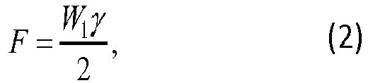

- Back to
figure 1 , the second jet beam NJ2 associated to the second contact area 101e2 is refracted at the angle Θ B2 into the medium with higher refractive index. Assuming n2 > n3 we determine angle Θ B2 as:
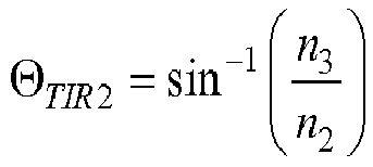
- Accordingly, the third jet beam NJ3 associated to the third contact area 101e3 is refracted at the angle Θ B3 with :


- We note that the length and intensity of the three jet beams NJ1, NJ2 and NJ3, are different. The maximal intensity and minimal length correspond to the beam with highest ratio between the refractive indexes. So, it is the first jet beam NJ1 refracted at the angle Θ B1 when n2 > n3> n1.
- To explain the behavior of the focused electromagnetic beam radiated by the
device 100, we can determine the points of intersection of the three jet beams NJ1, NJ2 and NJ3 radiated respectively at the angles Θ B1, Θ B2 and Θ B3. The point A of intersection of the first NJ1 and second NJ2 jet beams has the coordinates (W A, H A) in the XoZ coordinate system offigure 1 . More particularly, based on the previous equations one can get:
- Defining Θ B4 as the angle of deviation of the focal point A from the axis of symmetry 101as of the
first part 101 with width W1, one can get:
- In the same way, the first NJ1 and third NJ3 jet beams intersect at point B with the coordinates (W B, H B), where:

- Defining Θ B5 as the angle of deviation of the focal point B from the axis of a symmetry of the device 100 (i.e. the Z-axis in
figure 1 ) with width W1+W2, one gets:
- We note that the second NJ2 and third NJ3 jet beams intersect only if n3 is above a critical value, i.e. if


- In this case, defining Θ B6 as the angle of deviation of the focal point C from the axis of symmetry 102as of the
second part 102 with width W2, one gets:
- The particular case where the three jet beams NJ1, NJ2 and NJ3 intersect at the same point for fixed refractive indexes of the two
parts host medium 103 can be obtained as the result of variation of the widths W1, W2 of the twoparts 
- In this case, all three jet beams NJ1, NJ2 and NJ3 contribute to the total generated focused electromagnetic beam radiated by the
device 100. Thus, the intensity of the generated focused electromagnetic beam is maximal. - The dependencies of the deviation angles Θ B4-B6 on the refractive index n3 for fixed value n2=1.8 and W 1= W 2 are presented in
Figure 2 . For the chosen parameters, the critical value n3cr of refractive index n3 is given by
- Based on the identified properties of the
device 100 depicted infigure 1 , we review in the following how to adapt the parameters of the device 100 (i.e. the refractive index values, and/or the widths and/or the heights of constitutive first 101 and second 102 parts) in order to obtain a tilt of the generated focused electromagnetic beam (resulting from the combination of at least two beams among the first NJ1, second NJ2 and third NJ3 jet beams) in respect of the direction of propagation of the incoming electromagnetic wave IEM. - The numerical simulations discussed in the sequel have been performed assuming that H1=H2=H, that W1=W2, and that W=W1+W2 is greater than the equivalent wavelength in vacuum, λ, of the incoming electromagnetic wave IEM (However, as discussed above in relation with
figure 1 , the technical effects - i.e. having the electromagnetic field lines of the outgoing focused electromagnetic beam presenting a curvature - is achieved even if H1 and H2 are different from each other as long as we have |H2 - H1| ≤ λ/4). - Under the present assumptions, it can be shown that the hot spots positions of the generated jet beams are almost independent on the height H of the
device 100 for
Figure 3a for n 3= 1.3. - For

Figure 3b . For the parameters of thedevice 100 chosen for the simulation depicted infigure 3b , we get that HA≈772nm. - To explain this phenomenon let us consider the power density distribution in the XZ-plane. More particularly,
Figure 4a to 4c display the power density distribution in the XZ-plane for three different heights H=H1=H2 of thedevice 100 assuming that
device 100.Figure 4d presents the schematic distribution of the jet beams exited in the system. As a result, the curvature of the electromagnetic field lines of the outgoing focused electromagnetic beam takes place if H1 ≥ HA and if the focal point A for the first NJ1 and the second NJ2 jet beams is close to the radiatingsurface 100r of thedevice 100, or even within the device 100 (seeFigure 4d ). It can be seen, that in this case the curvature of the electromagnetic field lines of the outgoing focused electromagnetic beam is caused by an interplay of the second NJ2 and third NJ3 jet beams, which are longer but less intensive than the first NJ1 jet beam. The angle of deviation of the generated focused electromagnetic beam is close to the angle Θ B6 of deviation of the focal point C from the axis of symmetry 102as of thesecond part 102 with width W2 (red dash-dot line inFigure 4d ). -
Figures 5a and 5b show the dependencies of the hot spots positions of the jet beams generated by the device 100 (along the X and Z axis respectively) on the refractive index n 3 for three different heights H=H1=H2 of the system. More particularly, the light gray and the dash-dot lines indicate respectively the dependencies of the X and Z coordinates for points A and B on n 3. These two curves are calculated using equations (5) and (7). The power density of the hot spots as a function of n3 is presented inFigure 5c . - The equivalent wavelength in vacuum λ of the incoming electromagnetic wave influences the hot spots positions of the generated jet beams.
Figures 6a and 6b show the dependency of the hot spots shift on λ for different heights H=H1=H2. We note that for n 3= 1.3 the shift of the hot spots is almost independent on the wavelength λ. The influence of the dispersion rises with the refractive index n 3 (seeFigures 6b for n 3= 1.6). - Thus, in some embodiments of the present disclosure, the
device 100 is configured such as
illumination face 100i, of the intersection point of the first NJ1 and second NJ2 jet beams). This allows obtaining a tilt of the direction of the generated focused electromagnetic beam (that results from a combination of at least two beams among the first NJ1, second NJ2 and third NJ3 jet beams) in respect of the direction of propagation of the incoming electromagnetic wave IEM. - We now detail the influence of the width W1 and W2 of the first 101 and second 102 parts of the
device 100. - For that, we first analyze the influence of the width W2 of the
second part 102, having the refractive index n 3, on the parameters of the generated jet beams assuming a fixed width W1 of thefirst part 101 that has the refractive index n 2 (n2 > n3> n1). - More particularly, for

device 100 when W 2>W 1 as illustrated inFigure 7a . We see that the angle of deviation of the first jet beam NJ1 (beam number 1 inFigure 7a ) and of the second jet beam NJ2 (beam number 2 inFigure 7a ) are equal to Θ B4 and Θ B5 (seeFigure 7b ). Thus, the position and the intensity of the hot spot (i.e. the point of highest intensity in the jet beam) of the second jet beam NJ2 depend on the width W 2. The power density distribution along the X-axis at different widths W2 of thesecond part 102 of thedevice 100 is presented inFigure 7c . We see that the intensity and length of the second jet beam NJ2 rises with W 2. We also get that increasing the total width W=W1+W2 of thedevice 100 increases the input of Fresnel diffraction phenomenon into the total response of the system. So, the number of side jets of second type (or secondary lobes) deviated at an angle Θ B5 that rises as W 2 increases. - Alternatively, when

Figure 8a ). The angle of deviation of the third jet beam NJ3 (beam number 3 inFigure 8a ) associated to the third contact area 100e3 is equal to Θ B6 (seeFigure 8b ). The central jet beam (beam number 4 inFigure 8a ) is directed along the Z-axis (normal to the radiating face 100r of the device). The power density in the hot spots of the jet beams number 2-4 inFigure 8a and the position of the corresponding jet beams' hot spots versus the width W 2 of thesecond part 102 are presented inFigure 8b to 8e . As discussed above in the case where
- Thus, in some embodiments of the present disclosure, the
device 100 is configured such that
- Let us now analyze the influence of the width W1 of the
first part 101 having the refractive index n 2, on the parameters of the generated jet beams assuming a fixed width W2 of thesecond part 102 that has the refractive index n 3 (n2 > n3 > n1). - In fact, a similar behavior can be observed as in the previous case discussed above where W2 was varying for a fixed value of W1. However, in the present case the side jet beams (or secondary lobes) are deviated toward the angles Θ B4 (for the side jet beams on the left side when looking at the figures) and Θ B6 (for the side jet beams on the right side when looking at the figures). As mentioned above, in accordance with equation (11) we can intensify the generated focused electromagnetic beam based on some particular dimensions of the
device 100. For the values of the parameters of the system as chosen infigures 9a -d, the intersection of all the jet beams occurs when W1= 1960nm. InFigure 9d , the maximal intensity of the generated focused electromagnetic beam corresponds to W1≈1600nm. The maximal benefit connected with intersection of all jet beams at the same point will be observed at W ≈ λ, where W=W1+W2. - Thus, in some embodiments of the present disclosure, the
device 100 is configured such that
- We note that with the sizes W 1 > W 2, the deviation to the right (when looking at the figures) will be observed for

Figure 10a ) and even at lower heights H1, H2 of theparts device 100 when
Figure 10b ). Several factors are responsible for these phenomena. First of all, increasing the width W 1 increases the distance H A. Thus, the main contributor to the total focused electromagnetic beam radiated by thedevice 100 is done by the longer jet beams NJ2 and NJ3 radiated at the angles Θ B2 and Θ B3. - Thus, in some embodiments of the present disclosure, the
device 100 is configured such that
- Examination of power density distributions obtained for different oblique angles of incidence, α, (i.e. the angle of incidence of the incoming electromagnetic wave IEM relative to a normal of the
illumination face 100i) shows that the tilt of the direction of the generated focused electromagnetic beam in respect of the normal to the radiating face 100r is sensitive to the height of thedevice 100. - For example, for a system comprising the
device 100 in contact with adielectric host medium 103 such that n1=1, n2=1.8, n3=1.6, W1=1000nm, W2= 700nm, H1=H2=H=300nm and α=10°, the tilt angle γ of deviation of the generated focused electromagnetic beam from the normal incidence is equal to 14.49° and remains constant for all wavelengths of incident wave in the theoretical hypothesis of non-dispersive materials. The slight dispersion in the case of α=10° is observed for H= 550nm. Moreover, the angle γ is approximately equal to 17.54°. The dispersion of the system rises with the height H. The comparison ofFigure 11a and Figure 11b shows that for H= 900nm, the dispersion for normal illumination is lower than the dispersion for an oblique one. Moreover, for α=10° the angle γ of deviation of the generated focused electromagnetic beam changes from ≈21° to ≈18.9° for 450nm<λ<650nm. We also notice that for this height H=H1=H2 of thedevice 100 the additional deviation is approximately equal to the angle of incidence. A similar behavior of the generated focused electromagnetic beam takes place for higher angles of incidence α. But in this case the dispersion of deviation will be higher. - One can note that the present simulations have been performed for H=H1=H2, however, as discussed above, the conclusion remains the same as long as we have |H2 - H1| ≤ λ/4.
- In this section, we consider the device 100' of
figure 12 , i.e. with nonvertical edges (i.e. edges not parallel to the Z-axis) whereas the radiating 100r andillumination 100i faces both remain orthogonal to the Z-axis. Let us define αj (with j equal to 1, 2 or 3) as the base angles for a double-material system. With αj different from 90°, the device 100' may correspond to a double-material prismatic device in contact with adielectric host medium 103, with a refractive index n1 < n3< n2. - It can be shown that for the device 100'with the base angles αj > 90°-Θ Bj (with j equal to 1, 2 or 3) the corresponding jet beam radiation angle can be determined using the approximate formula:

- To get the approximate formula for θ* TIRj we have to consider the changing of the position of the contact areas compared to the configuration of the
device 100 offigure 1 . As a result, the corresponding jet beams radiation angle can be estimated as:
- These expressions can then be injected into the equations (4)-(11) for having a description of the behavior of the jet beams associated to the contact areas 100'e1, 100'e2 and 100'e3 of the device 100'.
- To consider the effect of the first 101' and second 102' parts with nonvertical contact areas 100'e1, 100'e2 and 100'e3, simulation results are discussed below that show the influence of the height H1=H2=H of the first 101' and second 102' parts on the generated jet beams when the total width W'=W'1+W'2 is such that W'>λ with W'1=W'2. It is seen that the hot spot position is almost independent on the height H' of the device 100' that is in contact with the
dielectric host medium 103 when
Figure 13a for n3=1.3). For
Figure 13b . For the parameters of the device 100' and of thedielectric host medium 103 chosen in thosefigures 13a and 13b , we get that HA≈718.96 nm. - To explain a last phenomenon observed in
Figure 14a to 14c we present the power density distribution in the XZ-plane for 3 different heights H'=H'1=H'2 of the device 100' with
- More particularly,
Figures 15a to 15d give the height HA and the deviation angle Θ B6 as obtained based on equations (5) and (10). InFigure 15a we see that varying the angle α 1 at fixed angles α 2 and α 3 affects only the specific height HA without changing the angle Θ B6 (for the parameters chosen for the simulation plotted inFigure 15a , we get that Θ B6=22°). Conversely, decreasing or increasing the base angle α 2 leads to the changing of both parameters HA and Θ B6 as can be seen inFigure 15b and 15c . We see that for the minimal angle α 2 we obtain a maximal deviation of the corresponding jet beam at minimal height H'=H'1=H'2 of the device 100'. - As can be seen in
Figure 15d , changing the base angle α3 does not only affect the specific height HA (for the parameters chosen for the simulation plotted inFigure 15d HA=718.96nm), but we also get that the maximal deviation is observed for the minimal angle α3.Figure 16 gives the power density distribution along the X-axis in the cut-plane Z0=1000nm for four different values of the angle α3, with λ=550nm, with α1=85°, α2=90° and with the device 100' having H'=H'1=H'2 greater than HA. - We now describe in relation with
figures 17a to 19d the possibility of subwavelength optical manipulation of micro- or nano-particles by the curved jet beams generated by a device (e.g. device 100 or 100') according to the disclosure. - More particularly, the optical forces acting on an arbitrary micro- or nano-particles can be calculated in an approximation of the particle by an electric dipole; this method applies for Rayleigh particles (particle much smaller than the incident wavelength) as detailed for instance in the article by P. Chaumet and M. Nieto-Vesperinas: "Time-averaged total force on a dipolar sphere in an electromagnetic field," Opt. Lett. 25, 1065-1067 (2000). Using the dipole approximation for the subwavelength radius of the sphere the force can be obtained as:


- The forces produced by the deviated jet beams in the presence or not of
obstacles 1800 have been simulated using Comsol software and based on the dipolar approximation for gold particles with a radius of 0.03µm and a dielectric permittivity ε = - 11.208+1.31184i. Further, those forces have been simulated on one hand for asingle material device 1710 having a refractive index n, and for the dual-material device 100 offigure 1 . - In
figures 17a and 17b , the devices are illuminated by a TM (for "Transverse magnetic") polarized incoming electromagnetic wave IEM with λ=550nm and α=0° (i.e. the incoming electromagnetic wave IEM has a direction of propagation orthogonal to theillumination face 100i of the device 100). Thesingle material device 1710 is made of the same material as thefirst part 101 of thedevice 100, i.e. n=n1=n2. Further thesingle material device 1710 has the same width W as thedevice 100, with W=W1+W2=2*600nm (W1=W2), and the same height H=H1=H2=900nm. The streamlines and arrows show the trajectories and directions of the optical forces obtained using the dipolar approximation. It is possible to see that in a case ofdouble material device 100 we can transport the particles along the curved trajectory. - Referring to
figures 18a to 19d , we describe the changing of the fields in a case when theobstacles 1800 are placed along the jet beams paths. The length of theobstacle 1800 in X-direction coincide with the width W1 of thefirst part 101 of thedevice 100. However, theobstacle 1800 is shifted between the axis of symmetry of theobstacle 1800 and the axis of symmetry thefirst part 101 by an offset equal to W 1/4. The same configuration is used for thesingle material device 1710. The simulations correspond to anobstacle 1800 made of glass with a refractive index 1.8 and a thickness equal to λ/8 placed at the distance 5λ/8 in the case ofFigures 18a to 18d , and made of metal (perfect electric conductor) with the same thickness λ/8 placed at the distance 3λ/8 in the case ofFigures 19a to 19d . We see that the presence of theobstacle 1800 leads to the disruption of the jet beams and to valuable changing in the trajectory. Increasing the refractive index of thesingle material device 1710, we get the curved trajectory but the forces pushing the particle away from the system are very small. Only the double-material device 100 (here with the height H=H1=H2=900nm) can generate the deviated jet beam. In that case, the particles can move along the curved trajectory around the obstacle. This effect was obtained for both type of obstacles 1800 (i.e. glass and metal). Moreover, in a case of conductingobstacles 1800 we can get trapping locations near the obstacle (white circle referred 1900 inFigure 19c ). - Thus, such double-
material device 100, 100' according to the disclosure (in any of its embodiment discussed above) can be used as an elementary part of an optical manipulation apparatus (e.g. an optical tweezer) 1700 for trapping or moving micro or nanoparticles in thedielectric host medium 103. For instance, the equivalent wavelength in vacuum, λ, of the incoming electromagnetic wave IEM belongs to the visible light spectrum (e.g. to the range going from 390nm to 700nm). - In some embodiments, such
optical manipulation apparatus 1700 can also comprise an optical source for radiating the incoming electromagnetic wave IEM that illuminates theillumination face 100i of thedevice 100, 100' (in any of its embodiments discussed above). In that case, theoptical manipulation apparatus 1700 can generate the tilted focused electromagnetic beam independently of the use of an external source for generating the incoming electromagnetic wave IEM.
Claims (10)
- Optical manipulation apparatus for trapping or moving micro or nanoparticles, characterized in that it comprises a device intended to be in contact with a dielectric host medium having a first refractive index n1 and in which said micro- or nano-particles are trapped or moved by a focused electromagnetic beam radiated by said device when an incoming electromagnetic wave illuminates at least one face of said device, named illumination face, said device comprising at least:- a first part of a first material having a second refractive index n2 and having a first width W 1 along a direction of extension of said illumination face, named X-axis; and- a second part of a second material having a third refractive index n3, with n1<n3<n2, and having a second width W 2 along said X-axis,said first and second parts being located side by side along said X-axis with W 1 + W 2 greater than an equivalent wavelength in vacuum, named λ, of said incoming electromagnetic wave, each of said first and second parts extending along a direction orthogonal to said illumination face, named Z-axis, from said illumination face up to another face of said device, named radiating face, opposite to said illumination face, said first and second parts having respectively a first height H1 and a second height H2 along said Z-axis fulfilling |H2 - H1| ≤ λ/4,
said device further comprising:- a first contact area intended to be between said host medium and said first part, said first contact area contributing to the radiation of a first jet beam in a near field zone when said incoming electromagnetic wave illuminates at least said illumination face;- a second contact area between said first part and said second part, said second contact area contributing to the radiation of a second jet beam in said near field zone when said incoming electromagnetic wave illuminates at least said illumination face; and- a third contact area intended to be between said second part and said host medium, said third contact area contributing to the radiation of a third jet beam in said near field zone when said incoming electromagnetic wave illuminates at least said illumination face,said focused electromagnetic beam resulting from a combination of at least two beams among said first, second and third jet beams, said device being configured for having a direction of propagation of said focused electromagnetic beam being tilted in respect of a direction of propagation of said incoming electromagnetic wave as a function of at least part of:- said first n1, second n2 and third n3 refractive indexes;- said first W 1 and second W 2 widths; and- said first H1 and second H2 heights. - Optical manipulation apparatus according to claim 1 wherein

- Optical manipulation apparatus according to claim 1 wherein

- Optical manipulation apparatus according to claim 1 wherein
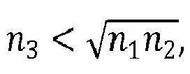
- Optical manipulation apparatus according to claim 1 wherein

- Optical manipulation apparatus according to any of the claims 2 to 5 wherein said height HA fulfils

- Optical manipulation apparatus according to claim 6 wherein Θ B1 and Θ B2 are targeted to be respectively equal to


- Optical manipulation apparatus according to claim 7 wherein


- Optical manipulation apparatus according to any of the claims 1 to 8 wherein said equivalent wavelength in vacuum, λ, of said incoming electromagnetic wave belongs to the visible light spectrum.
- Optical manipulation apparatus according to any of the claims 1 to 9 wherein at least one of said first and second materials belongs to the group comprising:- glass;- plastic;- a polymer material;- oxides; and- nitrides.
Priority Applications (5)
| Application Number | Priority Date | Filing Date | Title |
|---|---|---|---|
| EP18213584.8A EP3671310A1 (en) | 2018-12-18 | 2018-12-18 | Optical manipulation apparatus for trapping or moving micro or nanoparticles |
| US17/415,561 US12214493B2 (en) | 2018-12-18 | 2019-12-10 | Optical manipulation apparatus |
| EP19816721.5A EP3899632B1 (en) | 2018-12-18 | 2019-12-10 | Optical manipulation apparatus |
| PCT/EP2019/084526 WO2020126708A1 (en) | 2018-12-18 | 2019-12-10 | Optical manipulation apparatus |
| CN201980090828.1A CN113366365B (en) | 2018-12-18 | 2019-12-10 | Optical manipulation device |
Applications Claiming Priority (1)
| Application Number | Priority Date | Filing Date | Title |
|---|---|---|---|
| EP18213584.8A EP3671310A1 (en) | 2018-12-18 | 2018-12-18 | Optical manipulation apparatus for trapping or moving micro or nanoparticles |
Publications (1)
| Publication Number | Publication Date |
|---|---|
| EP3671310A1 true EP3671310A1 (en) | 2020-06-24 |
Family
ID=64745904
Family Applications (2)
| Application Number | Title | Priority Date | Filing Date |
|---|---|---|---|
| EP18213584.8A Withdrawn EP3671310A1 (en) | 2018-12-18 | 2018-12-18 | Optical manipulation apparatus for trapping or moving micro or nanoparticles |
| EP19816721.5A Active EP3899632B1 (en) | 2018-12-18 | 2019-12-10 | Optical manipulation apparatus |
Family Applications After (1)
| Application Number | Title | Priority Date | Filing Date |
|---|---|---|---|
| EP19816721.5A Active EP3899632B1 (en) | 2018-12-18 | 2019-12-10 | Optical manipulation apparatus |
Country Status (4)
| Country | Link |
|---|---|
| US (1) | US12214493B2 (en) |
| EP (2) | EP3671310A1 (en) |
| CN (1) | CN113366365B (en) |
| WO (1) | WO2020126708A1 (en) |
Families Citing this family (6)
| Publication number | Priority date | Publication date | Assignee | Title |
|---|---|---|---|---|
| EP3588150A1 (en) | 2018-06-29 | 2020-01-01 | Thomson Licensing | An optical device comprising multi-layer waveguides |
| EP3591700A1 (en) | 2018-07-02 | 2020-01-08 | Thomson Licensing | Image sensor comprising a color splitter with two different refractive indexes, and different height |
| EP3671310A1 (en) * | 2018-12-18 | 2020-06-24 | Thomson Licensing | Optical manipulation apparatus for trapping or moving micro or nanoparticles |
| EP3671322A1 (en) | 2018-12-18 | 2020-06-24 | Thomson Licensing | Device for forming an outgoing electromagnetic wave from an incident electromagnetic wave |
| EP3671293A1 (en) | 2018-12-21 | 2020-06-24 | Thomson Licensing | An optical device comprising at least one diffraction grating having a grating pitch above the wavelength |
| RU202241U1 (en) * | 2020-10-08 | 2021-02-08 | Федеральное государственное бюджетное образовательное учреждение высшего образования «Сибирский государственный университет геосистем и технологий» (СГУГиТ) | Subwavelength optical trap in a standing wave field based on a photonic jet |
Citations (4)
| Publication number | Priority date | Publication date | Assignee | Title |
|---|---|---|---|---|
| US3718383A (en) * | 1971-04-19 | 1973-02-27 | Eastman Kodak Co | Plastic optical element having refractive index gradient |
| EP3223063A1 (en) | 2016-03-24 | 2017-09-27 | Thomson Licensing | Device for forming a field intensity pattern in the near zone, from incident electromagnetic waves |
| EP3312674A1 (en) * | 2016-10-21 | 2018-04-25 | Thomson Licensing | A photolithography device for generating pattern on a photoresist substrate |
| EP3385219A1 (en) * | 2017-04-07 | 2018-10-10 | Thomson Licensing | Method for manufacturing a device for forming at least one focused beam in a near zone |
Family Cites Families (116)
| Publication number | Priority date | Publication date | Assignee | Title |
|---|---|---|---|---|
| JP3891628B2 (en) | 1997-02-04 | 2007-03-14 | オリンパス株式会社 | Illumination optical system and endoscope system including the same |
| EP1118884A4 (en) | 1999-08-04 | 2005-04-06 | Nippon Sheet Glass Co Ltd | Echelon diffraction grating and optical waveguide element |
| JP4345256B2 (en) | 2001-02-14 | 2009-10-14 | 旭硝子株式会社 | Wavelength selective diffraction element and optical head device |
| JP4049553B2 (en) | 2001-06-25 | 2008-02-20 | 日本放送協会 | Stereoscopic image transmitting apparatus and stereoscopic image receiving apparatus |
| CN1526079A (en) | 2001-07-10 | 2004-09-01 | 住友电气工业株式会社 | Optical waveguide type diffraction grating element and manufacturing method thereof |
| WO2003025635A1 (en) | 2001-09-19 | 2003-03-27 | Technion Research & Development Foundation Ltd. | Space-variant subwavelength dielectric grating and applications thereof |
| AU2003257697A1 (en) | 2002-09-19 | 2004-04-08 | Sumitomo Electric Industries, Ltd. | Diffractive optical device and method for producing same |
| CN101241202A (en) * | 2003-01-24 | 2008-08-13 | 住友电气工业株式会社 | Diffraction grating element |
| JP4609318B2 (en) * | 2003-02-18 | 2011-01-12 | 住友電気工業株式会社 | Diffraction grating element |
| TWI319124B (en) | 2003-02-27 | 2010-01-01 | Asml Netherlands Bv | Stationary and dynamic radial transverse electric polarizer for high numerical aperture systems |
| CN100386653C (en) * | 2003-03-13 | 2008-05-07 | 旭硝子株式会社 | Diffractive elements and optical devices |
| KR101162135B1 (en) | 2003-03-13 | 2012-07-03 | 아사히 가라스 가부시키가이샤 | Diffraction element and optical device |
| US20040198582A1 (en) * | 2003-04-01 | 2004-10-07 | Borrelli Nicholas F. | Optical elements and methods of making optical elements |
| US20060250933A1 (en) | 2003-04-25 | 2006-11-09 | Asada Jun-Ichi | Optical diffraction device and optical information processing device |
| FI115169B (en) | 2003-05-13 | 2005-03-15 | Nokia Corp | Method and optical system for coupling light to a waveguide |
| JP5055694B2 (en) | 2003-12-26 | 2012-10-24 | 旭硝子株式会社 | Polarizing diffraction element and optical head device |
| CN101614837A (en) | 2003-12-26 | 2009-12-30 | 旭硝子株式会社 | Polarization diffraction element and optical head device |
| US7456384B2 (en) | 2004-12-10 | 2008-11-25 | Sony Corporation | Method and apparatus for acquiring physical information, method for manufacturing semiconductor device including array of plurality of unit components for detecting physical quantity distribution, light-receiving device and manufacturing method therefor, and solid-state imaging device and manufacturing method therefor |
| CN1322339C (en) * | 2005-06-08 | 2007-06-20 | 中国科学院上海光学精密机械研究所 | High diffraction efficiency quartz transmission grating with 532 nm wavelength |
| NZ565682A (en) | 2005-07-08 | 2009-11-27 | Univ Illinois | Photonic crystal biosensor fabrication method |
| US7479404B2 (en) | 2005-07-08 | 2009-01-20 | The Board Of Trustees Of The University Of Illinois | Photonic crystal biosensor structure and fabrication method |
| US20090097122A1 (en) | 2005-09-14 | 2009-04-16 | Mirage Innovations Ltd | Diffractive Optical Device and System |
| FR2902226B1 (en) | 2006-06-12 | 2010-01-29 | Commissariat Energie Atomique | OPTICAL COMPONENT OPERATING IN NEAR FIELD TRANSMISSION |
| JP4893200B2 (en) | 2006-09-28 | 2012-03-07 | ブラザー工業株式会社 | Optical system for light beam transfer, and retinal scanning display using the same |
| US8212859B2 (en) | 2006-10-13 | 2012-07-03 | Apple Inc. | Peripheral treatment for head-mounted displays |
| WO2008073439A2 (en) | 2006-12-08 | 2008-06-19 | The City University Of New York Technology Commercialization Office | Devices and methods for light control in material composites |
| US7394535B1 (en) | 2007-03-20 | 2008-07-01 | Tokyo Electron Limited | Optical metrology using a photonic nanojet |
| JP5294584B2 (en) | 2007-07-27 | 2013-09-18 | キヤノン株式会社 | Optical element and optical apparatus |
| CN101359094B (en) * | 2007-07-31 | 2012-07-04 | 陈宽任 | Electro-magnetic wave transmission structure |
| WO2009083977A2 (en) | 2008-01-02 | 2009-07-09 | Mirage Innovations Ltd. | Optical device for relaying polychromatic light |
| US8384818B2 (en) | 2008-06-18 | 2013-02-26 | Panasonic Corporation | Solid-state imaging device including arrays of optical elements and photosensitive cells |
| US8717669B2 (en) | 2008-10-17 | 2014-05-06 | The Arizona Board Of Regents | Apparatus and method of generating nearly non-diffracting beams from multimode optical fibers |
| US8078027B2 (en) | 2008-12-03 | 2011-12-13 | National Cheng Kung University | Focus enhancing electromagnetic wave propagating device |
| EP2196729A1 (en) | 2008-12-12 | 2010-06-16 | BAE Systems PLC | Improvements in or relating to waveguides |
| CN101799589B (en) | 2009-02-09 | 2013-05-08 | 财团法人工业技术研究院 | Color separation optical element and image panel device |
| PL2229938T3 (en) | 2009-03-13 | 2012-09-28 | Sanovel Ilac Sanayi Ve Ticaret As | Ezetimibe compositions |
| JP4743917B2 (en) | 2009-08-25 | 2011-08-10 | Necシステムテクノロジー株式会社 | Optical unit |
| JP2012015424A (en) | 2010-07-02 | 2012-01-19 | Panasonic Corp | Solid-state imaging device |
| BR112013001536A2 (en) * | 2010-07-22 | 2019-09-24 | Univ Pittsburgh Commonwealth Sys Higher Education | vertical dipole array structures, methods of producing vertical dipole array structures and forming large-area vertical nano-aperture arrays, photovoltaic devices and 2d and vertical dipole nano-aperture arrays |
| JP5476247B2 (en) | 2010-07-26 | 2014-04-23 | 日本発條株式会社 | Silencer for laminated leaf spring |
| JP6007830B2 (en) | 2012-03-26 | 2016-10-12 | 旭硝子株式会社 | Transmission diffraction element |
| US8989535B2 (en) | 2012-06-04 | 2015-03-24 | Microsoft Technology Licensing, Llc | Multiple waveguide imaging structure |
| BR112015001491A2 (en) | 2012-07-25 | 2017-08-22 | Csem Centre Suisse D´Electronique Et De Microtechnique Sa Rech Et Developpement | METHOD TO OPTIMIZE A WAVEGUIDE BY LIGHT COUPLING |
| US9140602B2 (en) | 2012-08-11 | 2015-09-22 | The Board Of Trustees Of The Leland Stanford Junior University | Nanophotonic light-field sensor |
| FR2994602B1 (en) | 2012-08-16 | 2014-09-12 | Commissariat Energie Atomique | SPECTRAL FILTERING DEVICE IN VISIBLE AND INFRARED DOMAINS |
| US8885997B2 (en) | 2012-08-31 | 2014-11-11 | Microsoft Corporation | NED polarization system for wavelength pass-through |
| US9099370B2 (en) | 2012-09-03 | 2015-08-04 | Panasonic Intellectual Property Management Co., Ltd. | Solid-state imaging element and imaging device |
| FI125270B (en) | 2012-09-20 | 2015-08-14 | Teknologian Tutkimuskeskus Vtt Oy | Optical device with diffractive grating |
| JP6011826B2 (en) | 2012-10-18 | 2016-10-19 | パナソニックIpマネジメント株式会社 | Solid-state image sensor |
| FR2998979B1 (en) | 2012-11-30 | 2017-09-08 | Office National Detudes Et De Rech Aerospatiales Onera | DEVICE FOR CONTROLLING THE PHASE OF AN OPTICAL WAVEFRONT |
| JP2014134564A (en) | 2013-01-08 | 2014-07-24 | Canon Inc | Absorption type wire grid polarization element and optical instrument |
| DE102013003441A1 (en) | 2013-02-25 | 2014-09-11 | Fraunhofer-Gesellschaft zur Förderung der angewandten Forschung e.V. | Electromagnetic radiation scattering element |
| WO2014176277A1 (en) | 2013-04-22 | 2014-10-30 | Cornell University | Athermal optical devices based on composite structures |
| JP6271900B2 (en) | 2013-07-31 | 2018-01-31 | キヤノン株式会社 | Solid-state imaging device and imaging apparatus using the same |
| US10371898B2 (en) | 2013-09-05 | 2019-08-06 | Southern Methodist University | Enhanced coupling strength grating having a cover layer |
| WO2015062641A1 (en) | 2013-10-29 | 2015-05-07 | CSEM Centre Suisse d'Electronique et de Microtechnique SA - Recherche et Développement | Optical grating coupling structure |
| KR102276432B1 (en) | 2014-04-07 | 2021-07-09 | 삼성전자주식회사 | Color separation device and image sensor including the color separation device |
| KR102159166B1 (en) | 2014-05-09 | 2020-09-23 | 삼성전자주식회사 | Color separation device and image sensor including the color separation device |
| US10440244B2 (en) | 2014-05-27 | 2019-10-08 | Technion Research & Development Foundation Limited | Near-field imaging devices |
| US9726794B2 (en) | 2014-06-13 | 2017-08-08 | The Regents Of The University Of California | High index contrast grating structure for light manipulation and related method |
| US10670972B2 (en) | 2014-06-13 | 2020-06-02 | Infineon Technologies Ag | Method and apparatus for exposing a structure on a substrate |
| KR102261855B1 (en) | 2014-06-13 | 2021-06-07 | 삼성전자주식회사 | Stacked image sensor including color separation element and image pickup apparatus including the stacked image sensor |
| US9304235B2 (en) | 2014-07-30 | 2016-04-05 | Microsoft Technology Licensing, Llc | Microfabrication |
| GB2529003B (en) | 2014-08-03 | 2020-08-26 | Wave Optics Ltd | Optical device |
| KR20160023158A (en) | 2014-08-21 | 2016-03-03 | 삼성전자주식회사 | Image sensor having improved light utilization efficiency and method of manufacturing the same |
| KR102323204B1 (en) | 2014-08-22 | 2021-11-08 | 삼성전자주식회사 | Image sensor vividly embodying color and method of manufacturing the same |
| KR102316447B1 (en) | 2014-08-28 | 2021-10-22 | 삼성전자주식회사 | Image sensor having improved light utilization efficiency |
| US20160064172A1 (en) | 2014-09-02 | 2016-03-03 | Delta Systems, Inc. | Plunger switch assembly and method of operation |
| KR102307458B1 (en) | 2014-10-20 | 2021-09-30 | 삼성전자주식회사 | Color splitter and method for manufacturing the same and image sensor including the same |
| US9513480B2 (en) | 2015-02-09 | 2016-12-06 | Microsoft Technology Licensing, Llc | Waveguide |
| US9827209B2 (en) | 2015-02-09 | 2017-11-28 | Microsoft Technology Licensing, Llc | Display system |
| EP3113478A1 (en) | 2015-06-30 | 2017-01-04 | Thomson Licensing | Plenoptic foveated camera |
| US10431624B2 (en) | 2015-07-08 | 2019-10-01 | Samsung Electronics Co., Ltd. | Method of manufacturing image sensor including nanostructure color filter |
| WO2017031366A1 (en) | 2015-08-19 | 2017-02-23 | President And Fellows Of Harvard College | Broadband multifunctional efficient meta-gratings based on dielectric waveguide phase shifters |
| EP3339938A4 (en) | 2015-08-20 | 2019-05-01 | Hoya Lens Thailand Ltd. | Optical device |
| KR102501643B1 (en) | 2015-09-24 | 2023-02-20 | 삼성전자주식회사 | Optical device having high refractive index optical functional layer and method of fabricating the same |
| KR102519178B1 (en) | 2015-09-25 | 2023-04-06 | 삼성전자주식회사 | Image sensor including color separation element and image pickup apparatus including the image sensor |
| KR102465995B1 (en) | 2015-09-30 | 2022-11-25 | 삼성전자주식회사 | Color splitter structure, method of manufacturing the same, image sensor including color splitter structure and optical apparatus including image sensor |
| KR102409389B1 (en) | 2015-10-06 | 2022-06-15 | 삼성전자주식회사 | Image sensor including color separation element |
| KR102556008B1 (en) | 2015-10-06 | 2023-07-17 | 삼성전자주식회사 | Color splitter of image sensor |
| KR102561097B1 (en) | 2015-12-22 | 2023-07-28 | 삼성전자주식회사 | Color separation element array, image sensor having the same, and electronic apparatus |
| US9927614B2 (en) | 2015-12-29 | 2018-03-27 | Microsoft Technology Licensing, Llc | Augmented reality display system with variable focus |
| US9720237B1 (en) | 2016-01-27 | 2017-08-01 | Microsoft Technology Licensing, Llc. | Mixed environment display device and waveguide cross-coupling suppressors |
| US9891436B2 (en) | 2016-02-11 | 2018-02-13 | Microsoft Technology Licensing, Llc | Waveguide-based displays with anti-reflective and highly-reflective coating |
| EP3223062A1 (en) | 2016-03-24 | 2017-09-27 | Thomson Licensing | Device for forming at least one focused beam in the near zone, from incident electromagnetic waves |
| US9791703B1 (en) | 2016-04-13 | 2017-10-17 | Microsoft Technology Licensing, Llc | Waveguides with extended field of view |
| US10197804B2 (en) | 2016-04-25 | 2019-02-05 | Microsoft Technology Licensing, Llc | Refractive coating for diffractive optical elements |
| US10061124B2 (en) | 2016-04-29 | 2018-08-28 | Microsoft Technology Licensing, Llc | Robust architecture for large field of view components |
| EP3240046A1 (en) | 2016-04-29 | 2017-11-01 | BASF Coatings GmbH | Solar light collector |
| KR20170137364A (en) * | 2016-06-03 | 2017-12-13 | 삼성전자주식회사 | Electromagnetic wave focusing device and optical apparatus including the same |
| CN105911711B (en) | 2016-06-24 | 2019-03-15 | 京东方科技集团股份有限公司 | a display device |
| CN109716177B (en) | 2016-09-15 | 2024-01-30 | 麦格纳国际公司 | Super surface lens assembly for chromaticity separation |
| US11204452B2 (en) * | 2016-10-05 | 2021-12-21 | Agency For Science, Technology And Research | Diffractive optical element and method of forming thereof |
| EP3312660A1 (en) | 2016-10-21 | 2018-04-25 | Thomson Licensing | Device for forming at least one tilted focused beam in the near zone, from incident electromagnetic waves |
| EP3312646A1 (en) | 2016-10-21 | 2018-04-25 | Thomson Licensing | Device and method for shielding at least one sub-wavelength-scale object from an incident electromagnetic wave |
| CN114879358B (en) | 2016-10-26 | 2025-03-28 | 奇跃公司 | Outcoupling Gratings for Augmented Reality Systems |
| CA3045014A1 (en) | 2016-12-01 | 2018-06-07 | Magic Leap, Inc. | Projector with scanning array light engine |
| EP3548939A4 (en) | 2016-12-02 | 2020-11-25 | DigiLens Inc. | WAVE GUIDE DEVICE WITH UNIFORM OUTPUT LIGHTING |
| CN106772734A (en) | 2017-01-03 | 2017-05-31 | 中国科学院上海光学精密机械研究所 | The asymmetric pattern reflection type optical grid of broadband high-diffraction efficiency |
| EP4628965A3 (en) | 2017-02-15 | 2025-12-17 | Magic Leap, Inc. | Projector architecture incorporating artifact mitigation |
| US10534115B1 (en) | 2017-09-22 | 2020-01-14 | Facebook Technologies, Llc | Gray-tone electron-beam lithography |
| EP3460561A1 (en) | 2017-09-26 | 2019-03-27 | Thomson Licensing | Device for deviating and focusing light |
| KR20250026388A (en) | 2017-10-20 | 2025-02-25 | 매직 립, 인코포레이티드 | Configuring optical layers in imprint lithography processes |
| EP3499278A1 (en) | 2017-12-13 | 2019-06-19 | Thomson Licensing | A diffraction grating structure comprising several grating lines |
| EP3540499A1 (en) * | 2018-03-13 | 2019-09-18 | Thomson Licensing | Image sensor comprising a color splitter with two different refractive indexes |
| EP3540479A1 (en) * | 2018-03-13 | 2019-09-18 | Thomson Licensing | Diffraction grating comprising double-materials structures |
| CN108508506A (en) | 2018-04-16 | 2018-09-07 | 东莞理工学院 | Dual-function device combining wave plate and optical device based on medium super surface |
| JP7310809B2 (en) | 2018-06-11 | 2023-07-19 | Agc株式会社 | Diffractive optical element, projection device and measurement device |
| CN108919399B (en) * | 2018-06-11 | 2020-10-16 | 中山大学 | High-refractive-index contrast grating and preparation method and application thereof |
| EP3588150A1 (en) | 2018-06-29 | 2020-01-01 | Thomson Licensing | An optical device comprising multi-layer waveguides |
| EP3591700A1 (en) * | 2018-07-02 | 2020-01-08 | Thomson Licensing | Image sensor comprising a color splitter with two different refractive indexes, and different height |
| KR102621592B1 (en) | 2018-08-23 | 2024-01-08 | 삼성디스플레이 주식회사 | Display device and manufacturing method thereof |
| EP3671310A1 (en) * | 2018-12-18 | 2020-06-24 | Thomson Licensing | Optical manipulation apparatus for trapping or moving micro or nanoparticles |
| EP3671322A1 (en) | 2018-12-18 | 2020-06-24 | Thomson Licensing | Device for forming an outgoing electromagnetic wave from an incident electromagnetic wave |
| EP3671293A1 (en) | 2018-12-21 | 2020-06-24 | Thomson Licensing | An optical device comprising at least one diffraction grating having a grating pitch above the wavelength |
| EP4031927B1 (en) | 2019-09-19 | 2024-10-30 | InterDigital Madison Patent Holdings, SAS | Optical device for coupling a high field of view of incident light |
-
2018
- 2018-12-18 EP EP18213584.8A patent/EP3671310A1/en not_active Withdrawn
-
2019
- 2019-12-10 EP EP19816721.5A patent/EP3899632B1/en active Active
- 2019-12-10 WO PCT/EP2019/084526 patent/WO2020126708A1/en not_active Ceased
- 2019-12-10 US US17/415,561 patent/US12214493B2/en active Active
- 2019-12-10 CN CN201980090828.1A patent/CN113366365B/en active Active
Patent Citations (4)
| Publication number | Priority date | Publication date | Assignee | Title |
|---|---|---|---|---|
| US3718383A (en) * | 1971-04-19 | 1973-02-27 | Eastman Kodak Co | Plastic optical element having refractive index gradient |
| EP3223063A1 (en) | 2016-03-24 | 2017-09-27 | Thomson Licensing | Device for forming a field intensity pattern in the near zone, from incident electromagnetic waves |
| EP3312674A1 (en) * | 2016-10-21 | 2018-04-25 | Thomson Licensing | A photolithography device for generating pattern on a photoresist substrate |
| EP3385219A1 (en) * | 2017-04-07 | 2018-10-10 | Thomson Licensing | Method for manufacturing a device for forming at least one focused beam in a near zone |
Non-Patent Citations (5)
| Title |
|---|
| A. S. ANG; A. KARABCHEVSKY; I. V. MININ; O. V. MININ; S. V. SUKHOV; A. S. SHALIN: "''Photonic Hook' based optomechanical nanoparticle manipulator", SCIENT. REP., 2018 |
| ANGELEENE S. ANG ET AL: "'Photonic Hook' based optomechanical nanoparticle manipulator", SCIENTIFIC REPORTS, vol. 8, no. 1, 1 February 2018 (2018-02-01), XP055565926, DOI: 10.1038/s41598-018-20224-4 * |
| CHEN XU ET AL: "Photon nanojet lens: design, fabrication and characterization", NANOTECHNOLOGY, IOP, BRISTOL, GB, vol. 27, no. 16, 4 March 2016 (2016-03-04), pages 165302, XP020303438, ISSN: 0957-4484, [retrieved on 20160304], DOI: 10.1088/0957-4484/27/16/165302 * |
| LIYANG YUE ET AL: "Photonic hook: a new curved light beam", OPTICS LETTERS, vol. 43, no. 4, 15 February 2018 (2018-02-15), US, pages 771, XP055457895, ISSN: 0146-9592, DOI: 10.1364/OL.43.000771 * |
| P. CHAUMET; M. NIETO-VESPERINAS: "Time-averaged total force on a dipolar sphere in an electromagnetic field", OPT. LETT., vol. 25, 2000, pages 1065 - 1067 |
Also Published As
| Publication number | Publication date |
|---|---|
| US12214493B2 (en) | 2025-02-04 |
| EP3899632A1 (en) | 2021-10-27 |
| WO2020126708A1 (en) | 2020-06-25 |
| CN113366365A (en) | 2021-09-07 |
| US20220059250A1 (en) | 2022-02-24 |
| CN113366365B (en) | 2024-10-18 |
| EP3899632B1 (en) | 2024-04-10 |
Similar Documents
| Publication | Publication Date | Title |
|---|---|---|
| EP3899632B1 (en) | Optical manipulation apparatus | |
| EP3765873B1 (en) | Diffraction grating comprising double-materials structures | |
| US11391866B2 (en) | High quality factor non-uniform metasurfaces | |
| Karásek et al. | Long-range one-dimensional longitudinal optical binding | |
| Szameit et al. | Hexagonal waveguide arrays written with fs-laser pulses | |
| US20030227415A1 (en) | Photonic crystal exhibiting negative refraction without requiring a negative effective index | |
| Radko et al. | Plasmonic metasurfaces for waveguiding and field enhancement | |
| US8755661B2 (en) | Electromagnetic wave propagating structure | |
| Du et al. | Dielectric-based extremely-low-loss subwavelength-light transport at the nanoscale: An alternative to surface-plasmon-mediated waveguiding | |
| US20090142016A1 (en) | Plasmonic optics for plasmonic circuits | |
| CN101359094B (en) | Electro-magnetic wave transmission structure | |
| EP3861399B1 (en) | Inhomogeneous microlens device for near-field focusing, beam forming, and high-efficiency far-field device implementation | |
| CN113039475B (en) | Equipment intended to radiate at least one outgoing electromagnetic wave when illuminated by an incident electromagnetic wave | |
| WO2013039452A1 (en) | Method and structure for coupling light into a waveguide comprising nano - sized scattering elements | |
| Coello et al. | Surface plasmon polariton excitation and manipulation by nanoparticle arrays | |
| Ploss et al. | Young’s double-slit, invisible objects and the role of noise in an optical epsilon-near-zero experiment | |
| Naserpour et al. | Accelerating wide-angle converging waves in the near field | |
| Zhang et al. | Airy resonances in photonic crystal superpotentials | |
| Cai et al. | The Working Principles and Applications of Plasmonic Optical Tweezers | |
| Chauhan et al. | Plasmonic Devices for Electromagnetic Wave Concentration | |
| Zhang et al. | TE-polarized beam shaping by a subwavelength metal slit: Finite-difference at frequency-domain simulations | |
| Wang et al. | Nanopatterned Photonics on Probe: Modeling, Simulations, and Applications for Near-Field Light Manipulation | |
| Hoffman | Propagation characteristics of plasmonic gap waveguiding structures | |
| Stockman | Department of Physics and Astronomy, Georgia State University Atlanta, Georgia 30303, USA | |
| Segovia et al. | Coupling of Surface-Plasmon Polariton in nano-arrays of particles |
Legal Events
| Date | Code | Title | Description |
|---|---|---|---|
| PUAI | Public reference made under article 153(3) epc to a published international application that has entered the european phase |
Free format text: ORIGINAL CODE: 0009012 |
|
| STAA | Information on the status of an ep patent application or granted ep patent |
Free format text: STATUS: THE APPLICATION HAS BEEN PUBLISHED |
|
| AK | Designated contracting states |
Kind code of ref document: A1 Designated state(s): AL AT BE BG CH CY CZ DE DK EE ES FI FR GB GR HR HU IE IS IT LI LT LU LV MC MK MT NL NO PL PT RO RS SE SI SK SM TR |
|
| AX | Request for extension of the european patent |
Extension state: BA ME |
|
| RAP1 | Party data changed (applicant data changed or rights of an application transferred) |
Owner name: THOMSON LICENSING |
|
| STAA | Information on the status of an ep patent application or granted ep patent |
Free format text: STATUS: THE APPLICATION IS DEEMED TO BE WITHDRAWN |
|
| 18D | Application deemed to be withdrawn |
Effective date: 20210112 |