JP4609318B2 - Diffraction grating element - Google Patents
Diffraction grating element Download PDFInfo
- Publication number
- JP4609318B2 JP4609318B2 JP2005502667A JP2005502667A JP4609318B2 JP 4609318 B2 JP4609318 B2 JP 4609318B2 JP 2005502667 A JP2005502667 A JP 2005502667A JP 2005502667 A JP2005502667 A JP 2005502667A JP 4609318 B2 JP4609318 B2 JP 4609318B2
- Authority
- JP
- Japan
- Prior art keywords
- medium
- diffraction grating
- plane
- refractive index
- grating element
- Prior art date
- Legal status (The legal status is an assumption and is not a legal conclusion. Google has not performed a legal analysis and makes no representation as to the accuracy of the status listed.)
- Expired - Lifetime
Links
- 238000005530 etching Methods 0.000 claims description 27
- 239000000463 material Substances 0.000 claims description 27
- 229910004298 SiO 2 Inorganic materials 0.000 claims description 7
- 229910018072 Al 2 O 3 Inorganic materials 0.000 claims description 6
- 229910010413 TiO 2 Inorganic materials 0.000 claims description 6
- 230000005540 biological transmission Effects 0.000 claims description 6
- OKTJSMMVPCPJKN-UHFFFAOYSA-N Carbon Chemical compound [C] OKTJSMMVPCPJKN-UHFFFAOYSA-N 0.000 claims description 5
- YCKRFDGAMUMZLT-UHFFFAOYSA-N Fluorine atom Chemical compound [F] YCKRFDGAMUMZLT-UHFFFAOYSA-N 0.000 claims description 5
- 229910017493 Nd 2 O 3 Inorganic materials 0.000 claims description 5
- 229910052799 carbon Inorganic materials 0.000 claims description 5
- 150000001875 compounds Chemical class 0.000 claims description 5
- 229910052731 fluorine Inorganic materials 0.000 claims description 5
- 239000011737 fluorine Substances 0.000 claims description 5
- CPLXHLVBOLITMK-UHFFFAOYSA-N magnesium oxide Inorganic materials [Mg]=O CPLXHLVBOLITMK-UHFFFAOYSA-N 0.000 claims description 5
- 239000007787 solid Substances 0.000 claims description 5
- 230000010287 polarization Effects 0.000 description 30
- 238000010586 diagram Methods 0.000 description 24
- 238000000034 method Methods 0.000 description 22
- 238000004519 manufacturing process Methods 0.000 description 21
- 239000010410 layer Substances 0.000 description 17
- 238000012986 modification Methods 0.000 description 16
- 230000004048 modification Effects 0.000 description 16
- 230000001629 suppression Effects 0.000 description 13
- 238000013461 design Methods 0.000 description 10
- 230000003287 optical effect Effects 0.000 description 10
- VYPSYNLAJGMNEJ-UHFFFAOYSA-N Silicium dioxide Chemical compound O=[Si]=O VYPSYNLAJGMNEJ-UHFFFAOYSA-N 0.000 description 9
- 101100177165 Caenorhabditis elegans har-1 gene Proteins 0.000 description 7
- 239000002356 single layer Substances 0.000 description 7
- 238000004458 analytical method Methods 0.000 description 6
- 230000000052 comparative effect Effects 0.000 description 6
- 238000005457 optimization Methods 0.000 description 4
- 229910016569 AlF 3 Inorganic materials 0.000 description 3
- 229910004261 CaF 2 Inorganic materials 0.000 description 3
- 238000004891 communication Methods 0.000 description 3
- 239000006185 dispersion Substances 0.000 description 3
- 230000000694 effects Effects 0.000 description 3
- 229910052739 hydrogen Inorganic materials 0.000 description 3
- 238000005229 chemical vapour deposition Methods 0.000 description 2
- 238000011161 development Methods 0.000 description 2
- 239000007789 gas Substances 0.000 description 2
- 239000005304 optical glass Substances 0.000 description 2
- 230000000737 periodic effect Effects 0.000 description 2
- 238000007790 scraping Methods 0.000 description 2
- 230000002238 attenuated effect Effects 0.000 description 1
- 230000015572 biosynthetic process Effects 0.000 description 1
- 230000003247 decreasing effect Effects 0.000 description 1
- 230000006866 deterioration Effects 0.000 description 1
- 230000002068 genetic effect Effects 0.000 description 1
- GPRLSGONYQIRFK-UHFFFAOYSA-N hydron Chemical compound [H+] GPRLSGONYQIRFK-UHFFFAOYSA-N 0.000 description 1
- 238000010884 ion-beam technique Methods 0.000 description 1
- 229910001635 magnesium fluoride Inorganic materials 0.000 description 1
- 239000002245 particle Substances 0.000 description 1
- 238000005498 polishing Methods 0.000 description 1
- 239000004065 semiconductor Substances 0.000 description 1
- 238000002922 simulated annealing Methods 0.000 description 1
- 230000005469 synchrotron radiation Effects 0.000 description 1
- 238000002834 transmittance Methods 0.000 description 1
Images


Classifications
-
- G—PHYSICS
- G02—OPTICS
- G02B—OPTICAL ELEMENTS, SYSTEMS OR APPARATUS
- G02B5/00—Optical elements other than lenses
- G02B5/18—Diffraction gratings
- G02B5/1866—Transmission gratings characterised by their structure, e.g. step profile, contours of substrate or grooves, pitch variations, materials
-
- G—PHYSICS
- G02—OPTICS
- G02B—OPTICAL ELEMENTS, SYSTEMS OR APPARATUS
- G02B6/00—Light guides; Structural details of arrangements comprising light guides and other optical elements, e.g. couplings
- G02B6/10—Light guides; Structural details of arrangements comprising light guides and other optical elements, e.g. couplings of the optical waveguide type
- G02B6/12—Light guides; Structural details of arrangements comprising light guides and other optical elements, e.g. couplings of the optical waveguide type of the integrated circuit kind
- G02B2006/12083—Constructional arrangements
- G02B2006/12107—Grating
Landscapes
- Physics & Mathematics (AREA)
- General Physics & Mathematics (AREA)
- Optics & Photonics (AREA)
- Diffracting Gratings Or Hologram Optical Elements (AREA)
Description
本発明は、透過型の回折格子素子に関するものである。 The present invention relates to a transmissive diffraction grating element .
回折格子素子は、一般に、互いに平行な第1面および第2面を有する透明平板において第1面に回折格子が形成されたものである(例えば、小舘香椎子、「回折光学の発展と新展開」、日本女子大学紀要、理学部、第10号、pp.7-24, (2002)を参照)。この回折格子素子では、例えば、第1面に接する媒質から該第1面に光が一定入射角で入射すると、その光は、第1面に形成された回折格子により回折され、透明平板の内部を通過して、第2面に接する媒質へ出射される。透明平板の第2面から出射されるときの光の回折角は、波長によって異なる。 A diffraction grating element is generally a transparent flat plate having a first surface and a second surface parallel to each other, and a diffraction grating is formed on the first surface (for example, Kyoko Ogura, “Development and New Development of Diffraction Optics”). "See the bulletin of Japan Women's University, Faculty of Science, No. 10, pp.7-24, (2002)). In this diffraction grating element, for example, when light is incident on the first surface at a constant incident angle from a medium in contact with the first surface, the light is diffracted by the diffraction grating formed on the first surface, and the inside of the transparent flat plate And is emitted to the medium in contact with the second surface. The diffraction angle of light when emitted from the second surface of the transparent flat plate varies depending on the wavelength.
このように、この回折格子素子は、入射した光を分波して出射する光分波器として用いられ得る。また、この回折格子素子は、上記の場合とは逆の方向に光を導く場合には、入射した光を合波して出射する光合波器として用いられ得る。さらに、回折格子素子と他の光学素子とを組み合わせることで、例えば、波長に応じて光の群遅延時間を調整する分散調整器を構成することもできる。したがって、回折格子素子は、多波長の信号光を多重化して伝送する波長分割多重(WDM: Wavelength Division Multiplexing)光通信システムにおいて重要な光デバイスの1つとなっている。 Thus, this diffraction grating element can be used as an optical demultiplexer that demultiplexes incident light and emits it. In addition, this diffraction grating element can be used as an optical multiplexer that combines and emits incident light when guiding light in the direction opposite to that described above. Furthermore, by combining a diffraction grating element and another optical element, for example, a dispersion adjuster that adjusts the group delay time of light according to the wavelength can be configured. Therefore, the diffraction grating element is one of important optical devices in a wavelength division multiplexing (WDM) optical communication system that multiplexes and transmits multi-wavelength signal light.
このような回折格子素子では回折効率が高いことが要求される。そして、回折効率向上の為の構造上の工夫が幾つか提案されており、95%程度の回折効率が報告されている(例えば、米国特許出願公開第2002/0135876号明細書や、Hendrick J. Gerritsen, et al., "Rectangular surface-relief transmission gratings with a very large first-order diffraction efficiency(〜95%) for unpolarized light", Applied Optics, Vol.37, No.25, pp.5823-5829 (1998)、を参照)。 Such a diffraction grating element is required to have high diffraction efficiency. Some structural ideas for improving the diffraction efficiency have been proposed, and a diffraction efficiency of about 95% has been reported (for example, US Patent Application Publication No. 2002/0135876, Hendrick J. et al. Gerritsen, et al., "Rectangular surface-relief transmission gratings with a very large first-order diffraction efficiency (~ 95%) for unpolarized light", Applied Optics, Vol.37, No.25, pp.5823-5829 (1998 )).
しかしながら、回折格子素子に入射する入射光の入射角、または、回折格子素子により回折されて出射する回折光の回折角は、0度(回折格子が形成された透明平板の第1面または第2面に垂直)では無く、反射による偏波依存性が発生する。また、回折格子は、一方向のみに周期的に屈折率が変化するという構造であるから、特に格子周期が短い(例えば2λ以下)ときに、周期方向と偏波方向との角度とが変わると、回折効率が変化する。このように、一般に、回折格子素子の回折効率は偏波依存性を有しており、TE偏波光およびTM偏波光それぞれの回折効率は互いに異なる。特に、回折角の角分散が大きい(合分波における波長分解能が高い)ときに、周期が短くなるから、偏波依存性は顕著になる。 However, the incident angle of the incident light incident on the diffraction grating element or the diffraction angle of the diffracted light emitted after being diffracted by the diffraction grating element is 0 degree (the first surface or the second surface of the transparent flat plate on which the diffraction grating is formed). Polarization dependence due to reflection occurs instead of (perpendicular to the surface). In addition, since the diffraction grating has a structure in which the refractive index changes periodically only in one direction, particularly when the grating period is short (for example, 2λ or less), the angle between the periodic direction and the polarization direction changes. The diffraction efficiency changes. As described above, generally, the diffraction efficiency of the diffraction grating element has polarization dependency, and the diffraction efficiency of the TE polarized light and the TM polarized light is different from each other. In particular, when the angular dispersion of the diffraction angle is large (the wavelength resolution in the multiplexing / demultiplexing is high), the period becomes short, so that the polarization dependency becomes remarkable.
TE偏波光およびTM偏波光それぞれの回折効率の差を低減するには、反射による偏波依存性と構造による偏波依存性とをキャンセルするように、回折格子の断面形状(格子の高さや幅など)を適切に設計することにより可能である。しかし、そのように設計した場合であっても、回折効率の向上および回折効率の偏波依存性の低減を広い波長域で実現することはできない。 To reduce the difference in diffraction efficiency between TE-polarized light and TM-polarized light, the cross-sectional shape of the diffraction grating (grating height and width) should be canceled so as to cancel the polarization dependence due to reflection and the polarization dependence due to structure. Etc.) can be designed properly. However, even in such a design, it is impossible to improve the diffraction efficiency and reduce the polarization dependence of the diffraction efficiency in a wide wavelength range.
本発明は、上記問題点を解消する為になされたものであり、反射による偏波依存性と構造による偏波依存性とを個別にキャンセルすることで、回折効率の向上および回折効率の偏波依存性の低減を広い波長域で実現することができる回折格子素子を提供することを目的とする。 The present invention has been made in order to solve the above-described problems. By separately canceling the polarization dependency due to reflection and the polarization dependency due to the structure, the diffraction efficiency can be improved and the polarization efficiency polarization can be improved. It is an object of the present invention to provide a diffraction grating element that can realize a reduction in dependence in a wide wavelength range .
本発明に係る回折格子素子は、複数の波長を含む光を分波又は合波する透過型の回折格子素子であって、平面を有する第1媒質(屈折率n 1 )と、第1媒質の平面に平行な平面を有する第4媒質(屈折率n 4 )と、第1媒質の平面と第4媒質の平面との間において、第1媒質の平面および第4媒質の平面に接して、第1媒質の平面に平行な所定方向に交互に設けられて回折格子を形成している第2媒質(屈折率n 2 )および第3媒質(屈折率n 3 、ただし、n 3 <n 2 )と、を備え、第1媒質、第2媒質、第3媒質および第4媒質それぞれの屈折率n 1 〜n 4 が「n 3 <n 1 <n 2 、n 3 ≦n 4 ≦n 2 」または「n 3 ≦n 1 ≦n 2 、n 3 <n 4 <n 2 」なる関係式を満たすことを特徴とする。さらに、第2媒質および第3媒質の双方が固体であることを特徴とし、或いは、第1媒質または第4媒質が等方性材料からなることを特徴とする。また、第1媒質の平面と第4媒質の平面との間における平均屈折率をn av としたときに、第1媒質の屈折率n 1 が「n av −0.2≦n 1 ≦n av +0.2」なる関係式を満たし、第4媒質の屈折率n 4 が「n av −0.2≦n 4 ≦n av +0.2」なる関係式を満たし、第2媒質の屈折率n 2 と第3媒質の屈折率n 3 との差が0.7以上であることを特徴とする。 A diffraction grating element according to the present invention is a transmission type diffraction grating element that demultiplexes or multiplexes light including a plurality of wavelengths, and includes a first medium (refractive index n 1 ) having a plane , A fourth medium having a plane parallel to the plane (refractive index n 4 ), and between the first medium plane and the fourth medium plane, in contact with the first medium plane and the fourth medium plane; A second medium (refractive index n 2 ) and a third medium (refractive index n 3 , where n 3 <n 2 ) alternately arranged in a predetermined direction parallel to the plane of one medium to form a diffraction grating; The refractive indexes n 1 to n 4 of the first medium, the second medium, the third medium, and the fourth medium are “n 3 <n 1 <n 2 , n 3 ≦ n 4 ≦ n 2 ” or “ The relational expression of n 3 ≦ n 1 ≦ n 2 and n 3 <n 4 <n 2 is satisfied. Furthermore, both the second medium and the third medium are solid, or the first medium or the fourth medium is made of an isotropic material. When the average refractive index between the plane of the first medium and the plane of the fourth medium is n av , the refractive index n 1 of the first medium is “n av −0.2 ≦ n 1 ≦ n av +0.2 ”, the refractive index n 4 of the fourth medium satisfies the relation “ n av −0.2 ≦ n 4 ≦ n av +0.2 ”, and the refractive index n 2 of the second medium. And the refractive index n 3 of the third medium is 0.7 or more.
本発明に係る回折格子素子では、第1媒質と第4媒質との間において、第2媒質と第3媒質とが交互に設けられて回折格子が形成されている。第1媒質から回折格子へ入射した光は、回折格子部において回折され、第4媒質へ出射される。或いは、第4媒質から回折格子へ入射した光は、回折格子部において回折され、第1媒質へ出射される。この回折格子素子は、各媒質の屈折率が上記関係式を満たしていることから、回折効率の向上および回折効率の偏波依存性の低減を広い波長域で実現することができる。 In the diffraction grating element according to the present invention, the second medium and the third medium are alternately provided between the first medium and the fourth medium to form a diffraction grating. The light that has entered the diffraction grating from the first medium is diffracted by the diffraction grating portion and emitted to the fourth medium. Alternatively, the light incident on the diffraction grating from the fourth medium is diffracted by the diffraction grating portion and emitted to the first medium. In this diffraction grating element, since the refractive index of each medium satisfies the above relational expression, it is possible to improve the diffraction efficiency and reduce the polarization dependence of the diffraction efficiency in a wide wavelength range.
また、第1平面に垂直な方向についての第1媒質の厚みが5μm以上であるのが好適であり、さらに、第1平面に垂直な方向についての第4媒質の厚みが5μm以上であるのが好適である。これらの場合には、回折効率の向上および回折効率の偏波依存性の低減を広い波長域で実現する上で更に好ましい。 The thickness of the first medium in the direction perpendicular to the first plane is preferably 5 μm or more, and the thickness of the fourth medium in the direction perpendicular to the first plane is 5 μm or more. Is preferred. In these cases, it is more preferable to improve the diffraction efficiency and reduce the polarization dependence of the diffraction efficiency in a wide wavelength region.
本発明に係る回折格子素子は、第2媒質がTiO2,Ta2O5およびNb2O5の何れかであるのが好適であり、第3媒質が気体であるのが好適である。こられの場合には、回折格子部の高さを低くすることができることから、回折格子素子の製造が容易である。 In the diffraction grating element according to the present invention, the second medium is preferably any one of TiO 2 , Ta 2 O 5 and Nb 2 O 5 , and the third medium is preferably a gas. In these cases, the diffraction grating element can be easily manufactured because the height of the diffraction grating portion can be reduced.
本発明に係る回折格子素子は、第2媒質または第3媒質がエネルギ線照射により屈折率が変化し得る所定材料からなるのが好適であり、所定材料がダイヤモンド様炭素であるのが好適である。これらの場合には、所望の特性を有する回折格子素子を容易に製造することができる。 In the diffraction grating element according to the present invention, the second medium or the third medium is preferably made of a predetermined material whose refractive index can be changed by energy beam irradiation, and the predetermined material is preferably diamond-like carbon. . In these cases, a diffraction grating element having desired characteristics can be easily manufactured.
本発明に係る回折格子素子は、第1媒質または第4媒質が、第2媒質または第3媒質よりエッチングレートが遅い所定材料からなるのが好適である。このように、エッチング層に接する非エッチング層のエッチングレートが遅い材料を用いるのが好ましく、例えば、エッチングレート比が2倍以上であるのが好適である。ここで、上記所定材料がAl2O3,MgO,Nd2O3およびフッ素系化合物の何れかであるのが好適であり、また、第2媒質または第3媒質がTiO2,Nb2O5,Ta2O5,SiN,SiO2,SiO,ZrO2,Sb2O3の何れかであるのが好適である。これらの場合には、回折格子素子をエッチング法により製造する上で好ましい。 In the diffraction grating element according to the present invention, it is preferable that the first medium or the fourth medium is made of a predetermined material having an etching rate slower than that of the second medium or the third medium. As described above, it is preferable to use a material with a slow etching rate of the non-etching layer in contact with the etching layer. For example, it is preferable that the etching rate ratio is twice or more. Here, the predetermined material is preferably Al 2 O 3 , MgO, Nd 2 O 3 or a fluorine-based compound, and the second medium or the third medium is TiO 2 , Nb 2 O 5. , Ta 2 O 5 , SiN, SiO 2 , SiO, ZrO 2 , or Sb 2 O 3 is preferable. In these cases, it is preferable to manufacture the diffraction grating element by an etching method.
以下、添付図面を参照して本発明の実施の形態を詳細に説明する。なお、図面の説明において同一の要素には同一の符号を付し、重複する説明を省略する。 Hereinafter, embodiments of the present invention will be described in detail with reference to the accompanying drawings. In the description of the drawings, the same elements are denoted by the same reference numerals, and redundant description is omitted.
(実施形態) ( Embodiment )
先ず、本発明に係る回折格子素子の実施形態について説明する。図1は、実施形態に係る回折格子素子10の説明図である。この図は、格子に垂直な面で切断したときの回折格子素子10の断面を示している。この図に示される回折格子素子10は、第1媒質11、第2媒質12、第3媒質13および第4媒質14を備えて構成されている。
First, description will be given of an embodiment of a diffraction grating element according to the present invention. Figure 1 is an explanatory diagram of a
この回折格子素子10において、互いに平行な第1平面P1および第2平面P2を仮想する。このとき、第1媒質11は、第1平面P1より外側(図では上側)に第1平面P1に接して設けられている。第2媒質12および第3媒質13は、第1平面P1と第2平面P2との間に、第1平面P1および第2平面P2に接して、第1平面P1に平行な所定方向に交互に設けられていて、回折格子を形成している。また、第4媒質14は、第2平面P2より外側(図では下側)に第2平面P2に接して設けられている。第2媒質12および第3媒質13の双方が固体であり、或いは、第1媒質11または第4媒質14が等方性材料からなる。
In this
この回折格子素子10では、第1媒質11と第4媒質14との間において、第2媒質12と第3媒質13とが交互に設けられて回折格子が形成されている。第1媒質11から回折格子へ入射した光Li(入射角θ)は、回折格子部において回折され、第4媒質14へ出射される(図1には、0次光Ld0、1次回折光Ld1が示されている)。或いは、第4媒質14から回折格子へ入射した光は、回折格子部において回折され、第1媒質11へ出射される。
In the
第2媒質12の各領域および第3媒質13の各領域は、何れも断面が長方形である。第2媒質12および第3媒質13が所定方向に交互に設けられることによって回折格子が形成された回折格子部において、その回折格子の周期をΛとし、その周期Λにおける第2媒質12が占める割合(デューティ比)をfとする。第1平面P1と第2平面P2との間の距離(すなわち、格子の高さ)をHとする。第1媒質11の屈折率をn1とし、第2媒質12の屈折率をn2とし、第3媒質13の屈折率をn3(ただし、n3<n2)とし、第4媒質14の屈折率をn4とする。
Each region of the
このとき、第1平面P1と第2平面P2との間の回折格子部の平均屈折率navは、

そして、回折格子の周期Λが入射光の波長λのオーダー以下(例えば2λ以下)であれば、第1平面P1および第2平面P2それぞれでの光の反射を考える際に、第1平面P1と第2平面P2との間を屈折率navの均質な媒質で置き換えことができる。このとき、第1媒質11の屈折率n1または第4媒質14の屈折率n4が回折格子部の平均屈折率navに近いほど、第1平面P1または第2平面P2における反射が低減され、回折特性が向上する。
If the period Λ of the diffraction grating is less than or equal to the order of the wavelength λ of the incident light (for example, 2λ or less), the first plane is considered when reflection of light on the first plane P 1 and the second plane P 2 is considered. A space between P 1 and the second plane P 2 can be replaced with a homogeneous medium having a refractive index n av . At this time, as the refractive index n 1 of the first medium 11 or the refractive index n 4 of the
そこで、本実施形態では、各媒質の屈折率n1〜n4は、
上記(3)式または(4)式に従って各媒質の屈折率n1〜n4が決定され、その後、厳密結合波解析法(RCWA: Rigorous Coupled-Wave Analysis)により回折格子素子10の回折特性の解析が行なわれる。そして、最適化手法(例えば、非線形計画法、シミュレーティドアニーリング法、遺伝アルゴリズムなど)により、デューティ比f、格子周期Λおよび格子高さHが最適化されることで、回折特性が優れた回折格子素子10が設計される。
The refractive indexes n 1 to n 4 of each medium are determined according to the above formula (3) or (4), and then the diffraction characteristics of the
次に、実施形態に係る回折格子素子10の実施例について、比較例とともに説明する。実施例1の回折格子素子10は、第1媒質11および第4媒質14それぞれが石英ガラス(n1=n4=1.45)であり、第2媒質12の屈折率n2が1.75であり、第3媒質13が空気(n3=1)であり、デューティ比fが0.70であり、格子周期Λが1.01μmであり、格子高さHが2.26μmである。比較例1の回折格子素子は、第1媒質および第3媒質それぞれが空気(n1=n3=1)であり、第2媒質および第4媒質それぞれが石英ガラス(n2=n4=1.45)であり、デューティ比fが0.84であり、格子周期Λが1.01μmであり、格子高さHが6.02μmである。
Next, examples of the
図2は、実施例1の回折格子素子10の回折特性を示すグラフである。図3は、比較例1の回折格子素子の回折特性を示すグラフである。これらの図には、光の入射角θが波長1.55μmにおけるブラッグ入射角であるときの回折効率の波長依存性がTE偏波光およびTM偏波光それぞれについて示されている。なお、ブラッグ入射角は、0次光および1次光それぞれの角度が等しくなる入射角をいう。また、これら実施例1および比較例1それぞれにおいては、波長帯域1.52μm〜1.57μmにおいて、回折効率の偏波依存性および波長依存性ができる限り小さく、回折効率ができる限り大きくなるように、各パラメータが設計された。
FIG. 2 is a graph showing the diffraction characteristics of the
これらの図を対比して判るように、比較例1の場合(図3)と比較して、実施例1の場合(図2)には、広い波長域で、TE偏波光およびTM偏波光それぞれの回折効率が高く95%以上であり、TE偏波光およびTM偏波光それぞれの回折効率の差が2%以下であった。このように、本実施形態に係る回折格子素子10は、回折効率の向上および回折効率の偏波依存性の低減を広い波長域で実現することができる。
As can be seen by comparing these figures, in the case of Example 1 (FIG. 2) compared to the case of Comparative Example 1 (FIG. 3), each of TE polarized light and TM polarized light in a wide wavelength range. The diffraction efficiency was 95% or more, and the difference in diffraction efficiency between TE polarized light and TM polarized light was 2% or less. As described above, the
図4は、実施例1の回折格子素子10の回折効率と第4媒質14の屈折率n4との関係を示すグラフである。ここでは、波長λは1.55μmに固定された。この図から判るように、第4媒質14の屈折率n4が上記(4b)式の関係式を満たす場合には、回折効率が大きく、偏波依存性が小さい。
FIG. 4 is a graph showing the relationship between the diffraction efficiency of the
次に、実施形態に係る回折格子素子10を製造する方法について幾つか説明する。
Next, several methods for manufacturing the
第1の製造方法では、第4媒質14の面上に第2媒質12からなる層を形成し、その層に対して所定の空間的パターンでエッチングにより溝を形成し、その上に第1媒質11を貼り合わせる。この場合、エッチングにより形成された溝の領域が、空気からなる第3媒質13となる。或いは、エッチングにより形成された溝の領域にCVD(Chemical Vapor Deposition)法等により第3領域13となるべき他の材料を埋め込み、研磨等により第2領域12および第3領域13それぞれの高さを揃えて、その上に第1媒質11を設けてもよい。ここで、第2領域12および第3領域13の双方が固体であれば、第1媒質11に貼り合わせる際の圧力による溝形状の変形を抑制することができ、また、CVD法等で第1媒質11を設ける際にも溝への第1媒質11の入り込みを抑制することができて、好適である。なお、第4媒質14の面上に第2媒質12からなる層を形成するのでは無く、第3媒質13からなる層を形成してもよい。
In the first manufacturing method, a layer made of the
第2媒質12または第3媒質13からなる層がエッチングされる際に、第4媒質14が、第2媒質12または第3媒質13よりエッチングレートが遅い所定材料からなるのが好ましく、この場合には、第4媒質14の上面(第2平面P2)でエッチングを終了させることができる。このような観点から、例えば、第4媒質14は、Al2O3,MgO,Nd2O3およびフッ素系化合物(AlF3,MgF2,CaF2,NdF3など)の何れかであるのが好ましい。また、第2媒質12または第3媒質13は、TiO2,Nb2O5,Ta2O5,SiN,SiO2,SiO,ZrO2,Sb2O3の何れかであるのが好ましい。
When the layer made of the second medium 12 or the third medium 13 is etched, the
なお、上記のエッチングに替えてリフトオフ等により第2媒質12および第3媒質13が交互に形成されてもよい。
Note that the
エッチングおよびリフトオフの何れの場合にも、格子高さHが低いほど溝形成が容易である。実施形態では、各媒質の屈折率n1〜n4それぞれを独立に設定することができるから、第2媒質12の屈折率n2と第3媒質13の屈折率n3との差(n2−n3)を大きくすることができ、したがって、格子高さHを低くすることができる。このような観点から、第2媒質12の屈折率n2と第3媒質13の屈折率n3との差(n2−n3)が0.7以上であれは、格子高さHを3μm以下とすることができ製造が容易となるので好適である。また、その為には、第2媒質12がTiO2,Ta2O5およびNb2O5の何れかであるのが好適であり、第3媒質13が気体であるのが好適である。また、第2媒質、第3媒質ともに固体の場合、第3媒質としてMgF2(屈折率1.35)のような低屈折率材料を用い、第2媒質として半導体、例えばSi(屈折率3.5)のような高屈折率材料を用いれば、さらに好適である。
In both cases of etching and lift-off, the lower the lattice height H, the easier the groove formation. In embodiments, since it is possible to independently set the respective refractive index n 1 ~n 4 of each medium, the difference between the refractive index n 3 of the refractive index n 2 and the
第2の製造方法では、第4媒質14の面上に、エネルギ線(例えばX線や粒子線など)の照射により屈折率が変化し得る所定材料からなる層を形成し、その層に対してエネルギ線を所定の空間的強度変調パターンで照射して、その層において互いに屈折率が異なる第2媒質12および第3媒質13が交互に設けられた回折格子を形成し、その上に第1媒質11を設ける。或いは、所定材料からなる層の上に第1媒質11を設け、その後に、その層に対してエネルギ線を所定の空間的強度変調パターンで照射して、その層において互いに屈折率が異なる第2媒質12および第3媒質13が交互に設けられた回折格子を形成するのも好適である。
In the second manufacturing method, a layer made of a predetermined material whose refractive index can be changed by irradiation with energy rays (for example, X-rays or particle rays) is formed on the surface of the
エネルギ線照射により屈折率が変化し得る所定材料としてダイヤモンド様炭素(DLC: Diamond-Like Carbon)が好適に用いられる。この場合、このダイヤモンド様炭素の屈折率を変化させる為に照射されるエネルギ線として、シンクロトロン放射光(SR光: Synchrotron Radiation)や水素イオンビームが用いられ、エネルギ線が照射されたダイヤモンド様炭素の領域の屈折率が大きくなる。すなわち、エネルギ線が照射されていない領域が第3媒質13(屈折率n3)となり、エネルギ線が照射された領域が第2媒質12(屈折率n2)となる。 Diamond-like carbon (DLC) is suitably used as a predetermined material whose refractive index can be changed by energy beam irradiation. In this case, synchrotron radiation (SR light) or a hydrogen ion beam is used as the energy rays irradiated to change the refractive index of the diamond-like carbon, and the diamond-like carbon irradiated with the energy rays. The refractive index of the region becomes larger. That is, the region not irradiated with the energy beam becomes the third medium 13 (refractive index n 3 ), and the region irradiated with the energy beam becomes the second medium 12 (refractive index n 2 ).
この第2の製造方法は、第1の製造方法と比較して、回折格子素子10の製造が簡略である点で好適である。また、第1の製造方法では、エッチングにより形成される溝の断面形状を完全な長方形とするのは困難であるが、これに対して、第2の製造方法では、第2媒質12および第3媒質13それぞれの各領域の断面形状がより完全な長方形となり得る点でも好適である。
This second manufacturing method is preferable in that the manufacturing of the
次に、実施形態に係る回折格子素子10の変形例について説明する。図5は、変形例1の回折格子素子10Aの説明図である。この図に示される変形例1の回折格子素子10Aは、上述した回折格子素子10の構成に対して、第1媒質11(屈折率n1)の外側(図では上側)に反射低減膜11aが形成され、更に反射低減膜11aの外側に媒質11b(屈折率n0)が存在し、また、第4媒質14(屈折率n4)の外側(図では下側)に反射低減膜14aが形成され、更に反射低減膜14aの外側に媒質14b(屈折率n5)が存在するものである。例えば、外側の媒質11bおよび媒質14bは、空気であり、或いは、回折格子素子10A全体の線膨張係数を調整して光学特性の温度依存性を低減する為の光学ガラスである。
Next, a description will be given of a variation of the
この変形例1の回折格子素子10Aでは、回折格子において発生するエバネセント波が充分に減衰するように、第1媒質11および第4媒質14それぞれの厚み(第1平面P1に垂直な方向についての厚み)は、波長λより充分に厚いのが好ましい。例えば、波長λが1.55μmであれば、第1媒質11および第4媒質14それぞれの厚みは5μm以上であるのが好適である。また、第1媒質11と外側の媒質11bとの間に反射低減膜11aが設けられ、また、第4媒質14と外側の媒質14bとの間に反射低減膜14aが設けられていることにより、これらの界面での反射が低減されて、回折特性の低下が抑制される。
In the diffraction
ここで、第1媒質11または第4媒質14が異方性材料からなる場合、偏波モード分散が発生し又は偏波状態が変化するので、光通信に影響を及ぼす。しかし、第1媒質11および第4媒質14を等方性材料のものとすることで、これらの影響を抑制することができ、また、反射低減膜11aや反射低減膜14aにおける反射低減の為の設計も容易になる。
Here, when the first medium 11 or the
図6は、変形例2の回折格子素子10Bの説明図である。図6においては、入射光Li、第4媒質14と媒質14bとの境界からの反射光Lr、回折光Ldそれぞれの軌跡が例示されている。この図に示される変形例2の回折格子素子10Bは、上述した回折格子素子10の構成に対して、第1媒質11(屈折率n1)の外側(図では上側)に媒質11b(屈折率n0)が存在し、また、第4媒質14(屈折率n4)の外側(図では下側)に媒質14b(屈折率n5)が存在するものである。例えば、外側の媒質11bおよび媒質14bは、空気であり、或いは、回折格子素子10A全体の線膨張係数を調整して光学特性の温度依存性を低減する為の光学ガラスである。特に、この変形例2の回折格子素子10Bでは、回折格子部での反射光・透過光・回折光が再び回折格子部に入射しないように、第1媒質11および第4媒質14それぞれは充分な厚みを有している。このことにより、回折特性の低下が抑制される。
FIG. 6 is an explanatory diagram of the diffraction
(第1参考形態) ( First reference form)
次に、回折格子素子の第1参考形態について説明する。図7は、第1参考形態に係る回折格子素子20の説明図である。この図は、格子に垂直な面で切断したときの回折格子素子20の断面を示している。この図に示される回折格子素子20は、第1媒質21、第2媒質22、第3媒質23、第4媒質24、第5媒質25および第6媒質26を備えて構成されている。
Next, a first reference embodiment of the diffraction grating element will be described. FIG. 7 is an explanatory diagram of the
この回折格子素子20において、互いに平行で順に並んだ第1平面P1、第2平面P2、第3平面P3および第4平面P4を仮想する。このとき、第1媒質21は、第1平面P1より外側(図では上側)に第1平面P1に接して設けられている。第2媒質22および第3媒質23は、第2平面P2と第3平面P3との間に、第2平面P2および第3平面P3に接して、第1平面P1に平行な所定方向に交互に設けられて、回折格子を形成している。第4媒質24は、第4平面P4より外側(図では下側)に第4平面P4に接して設けられている。第5媒質25は、第1平面P1と第2平面P2との間に、第1平面P1および第2平面P2に接して設けられている。第6媒質26は、第3平面P3と第4平面P4との間に、第3平面P3および第4平面P4に接して設けられている。
In this diffraction
この回折格子素子20では、第5媒質25と第6媒質26との間において、第2媒質22と第3媒質23とが交互に設けられて回折格子が形成されている。第1媒質21から回折格子へ入射した光は、第5媒質25を経て、回折格子部において回折され、第6媒質26を経て、第4媒質24へ出射される。或いは、第4媒質24から回折格子へ入射した光は、第6媒質26を経て、回折格子部において回折され、第5媒質25を経て、第1媒質21へ出射される。
In the
第2媒質22の各領域および第3媒質23の各領域は、何れも断面が長方形である。第2媒質22および第3媒質23が所定方向に交互に設けられることによって回折格子が形成された回折格子部において、その回折格子の周期をΛとし、その周期Λにおける第2媒質22が占める割合(デューティ比)をfとする。第1平面P1と第2平面P2との間の距離(すなわち、第5媒質25の厚み)をh5とする。第2平面P2と第3平面P3との間の距離(すなわち、格子の高さ)をHとする。第3平面P3と第4平面P4との間の距離(すなわち、第6媒質26の厚み)をh6とする。第1媒質21の屈折率をn1とし、第2媒質22の屈折率をn2とし、第3媒質23の屈折率をn3(ただし、n3<n2)とし、第4媒質24の屈折率をn4とし、第5媒質25の屈折率をn5とし、第6媒質26の屈折率をn6とする。
Each region of the
このとき、第2平面P2と第3平面P3との間の回折格子部の平均屈折率navは上記(1)式で表される。また、この平均屈折率navは、第2媒質22の屈折率n2および第3媒質23の屈折率n3との間で、上記(2)式の関係式を満たす。
At this time, the average refractive index n av of the diffraction grating portion between the second plane P 2 and the third plane P 3 is expressed by the above equation (1). Also, the average refractive index n av is between the refractive index n 3 of the refractive index n 2 and the
第5媒質25および第6媒質26それぞれは、反射低減の為の多層膜であってもよいし、単層の膜であってもよい。単層膜であるとき、第5媒質25の屈折率n5は、
![]()
![]()
さらに、第5媒質25の屈折率n5は、
また、界面での反射を広い波長帯域で低減する為には、第5媒質25の高さh5および第6媒質26の高さh6それぞれは、波長オーダー以下であることが好ましく、例えば5μm以下であるのが好適である。
Further, in order to reduce reflection at the interface in a wide wavelength band, the height h 6 each height h 5 and the
特に、第5媒質25中における波長λの光の角度をθ5とすると、第5媒質25の厚みh5は、
また、光がブラッグ角で入射するとすれば、上記(9)式は、
上記(5)式〜(12)式の何れかに従って各媒質の屈折率n1〜n6および厚みh5,h6が決定され、その後、RCWA法により回折格子素子20の回折特性の解析が行なわれる。そして、最適化手法により、デューティ比f、格子周期Λおよび格子高さHが最適化されることで、回折特性が優れた回折格子素子20が設計される。
The refractive indexes n 1 to n 6 and the thicknesses h 5 and h 6 of each medium are determined according to any of the above formulas (5) to (12), and then the diffraction characteristics of the
なお、以上では第5媒質25および第6媒質26それぞれが均一な単層膜であるとして説明してきたが、第5媒質25または第6媒質26が反射低減の為の多層膜であってもよい。後者の場合、TE偏波光およびTM偏波光それぞれの反射が抑制されて回折効率が向上し、多層膜の偏波依存性を利用することにより回折効率の偏波依存性を低減することができ、また、高次回折光やエバネセント波に対しても反射低減効果を期待することができる。
In the above description, each of the
次に、第1参考形態に係る回折格子素子20の参考例について説明する。参考例1の回折格子素子20は、第1媒質21が空気(n1=1)であり、第2媒質22がDLCのSR光照射部(n2=2.15)であり、第3媒質23がDLCのSR光非照射部(n3=1.55)であり、第4媒質24が石英ガラス(n4=1.45)であり、第5媒質25が石英ガラス(n5=1.45)であり、第6媒質26がMgO(n6=1.70)であった。デューティ比fが0.74であり、格子周期Λが1.01μmであり、格子高さHが3.35μmであり、第5媒質25の厚みh5が0.30μmであり、第6媒質26の厚みh6が0.23μmであった。
Next, a reference example of the
図8は、参考例1の回折格子素子20の回折特性を示すグラフである。この図には、光の入射角θが波長1.55μmにおけるブラッグ入射角であるときの回折効率の波長依存性がTE偏波光およびTM偏波光それぞれについて示されている。波長帯域1.52μm〜1.57μmにおいて、回折効率の偏波依存性および波長依存性ができる限り小さく、回折効率ができる限り大きくなるように、各パラメータが設計された。この図から判るように、参考例1の場合にも、広い波長域で、TE偏波光およびTM偏波光それぞれの回折効率が高く95%以上であり、TE偏波光およびTM偏波光それぞれの回折効率の差が2%以下であった。このように、本参考形態に係る回折格子素子20は、回折効率の向上および回折効率の偏波依存性の低減を広い波長域で実現することができる。
FIG. 8 is a graph showing the diffraction characteristics of the
次に、第1参考形態に係る回折格子素子20を製造する方法について説明する。上記実施形態の場合と略同様に、第1参考形態に係る回折格子素子20は、エッチング法やリフトオフ法を用いる第1の製造方法や、エネルギ線の照射により屈折率が変化し得る所定材料を用いる第2の製造方法により、製造することができる。ただし、第1参考形態では、第6媒質26は、第2媒質22または第3媒質23よりエッチングレートが遅い所定材料からなるのが好ましく、Al2O3,MgO,Nd2O3およびフッ素系化合物(AlF3,MgF2,CaF2,NdF3など)の何れかであるのが好ましい。
Next, a method for manufacturing the
次に、第1参考形態に係る回折格子素子20の変形例について説明する。回折格子素子20の変形例では、第5媒質25および第6媒質26の双方または何れか一方が所定方向に交互に設けられた複数の媒質からなる。
Next, a modification of the
図9は、変形例の回折格子素子20Aの説明図である。この図に示される変形例の回折格子素子20Aは、上述した回折格子素子20の構成に対して、第5媒質25および第6媒質26の双方が所定方向に交互に設けられた複数の媒質からなるものである。ここで、所定方向は、第2媒質22および第3媒質23が交互に設けられている方向と同じである。
FIG. 9 is an explanatory diagram of a modified diffraction
第5媒質25は、媒質25a(屈折率n5a)と媒質25b(屈折率n5b)とがΛ5で交互に設けられている。第6媒質26は、媒質26a(屈折率n6a)と媒質26b(屈折率n6b)とがΛ6で交互に設けられている。第5媒質25の周期Λ5における媒質25aが占める割合(デューティ比)をf5とし、第6媒質26の周期Λ6における媒質26aが占める割合(デューティ比)をf6とする。なお、第5媒質25の周期Λ5および第6媒質26の周期Λ6それぞれは、第2媒質22および第3媒質23からなる回折格子部の周期Λと等しいのが好適であり、或いは、周期Λの整数分の1であるのが好適である。また、第5媒質25の周期Λ5および第6媒質26の周期Λ6それぞれは、入射光の波長λと比べて充分に小さいのが好適であり、例えば波長λの1/5以下であるのが好適である。
In the
このとき、第5媒質25の平均屈折率n5は、
次に、この変形例の回折格子素子20の参考例について説明する。図10は、参考例2の回折格子素子20Bの説明図である。この参考例2の回折格子素子20Bでは、第5媒質25は所定方向に交互に設けられた2つの媒質25a,25bからなり、第6媒質26は均一である。参考例2の回折格子素子20Bは、第1媒質21が空気(n1=1)であり、第2媒質22がTa2O5(n2=2.0)であり、第3媒質23が空気(n3=1)であり、第4媒質24が石英ガラス(n4=1.45)であり、第5媒質25のうち媒質25aが石英ガラス(n5a=1.45)であって媒質25bが空気(n5b=1)であり、第6媒質26がAl2O3(n6=1.60)であった。デューティ比fおよびf5が0.66であり、格子周期Λが1.01μmであり、格子高さHが1.49μmであり、第5媒質25の厚みh5が0.36μmであり、第6媒質26の厚みh6が0.34μmであった。
Next, a reference example of the
図11は、参考例2の回折格子素子20Bの回折特性を示すグラフである。この図には、光の入射角θ(図10参照)が波長1.55μmにおけるブラッグ入射角であるときの回折効率の波長依存性がTE偏波光およびTM偏波光それぞれについて示されている。波長帯域1.52μm〜1.57μmにおいて、回折効率の偏波依存性および波長依存性ができる限り小さく、回折効率ができる限り大きくなるように、各パラメータが設計された。この図から判るように、参考例2の場合にも、広い波長域で、TE偏波光およびTM偏波光それぞれの回折効率が高く95%以上であり、TE偏波光およびTM偏波光それぞれの回折効率の差が2%以下であった。このように、第1参考形態に係る回折格子素子20は、回折効率の向上および回折効率の偏波依存性の低減を広い波長域で実現することができる。
FIG. 11 is a graph showing the diffraction characteristics of the diffraction
また、参考例2では、第2媒質22および第5媒質25を同時にエッチングすることができるので、製造が容易である。この際、第6媒質26として第2媒質22および第5媒質25よりエッチングレートが遅い所定材料を用いることで、製造する上で更に好都合である。また、第2媒質22、第5媒質25および第6媒質26を同時にエッチングすることも可能であり、この場合には、第4媒質24のエッチングレートが遅いのが好適である。
In the reference example 2 , the
(第2参考形態) ( Second reference form)
次に、回折格子素子の第2参考形態について説明する。図12は、第2参考形態に係る回折格子素子30の説明図である。この図は、格子に垂直な面で切断したときの回折格子素子30の断面を示している。この図に示される回折格子素子30は、第1媒質31、第2媒質32、第3媒質33、第4媒質34および第5媒質35を備えて構成されている。
Next, a second reference embodiment of the diffraction grating element will be described. FIG. 12 is an explanatory diagram of the
この回折格子素子30において、互いに平行で順に並んだ第1平面P1、第2平面P2および第3平面P3を仮想する。このとき、第1媒質31は、第1平面P1より外側(図では上側)に第1平面P1に接して設けられている。第2媒質32および第3媒質33は、第2平面P2と第3平面P3との間に、第2平面P2および第3平面P3に接して、第1平面P1に平行な所定方向に交互に設けられて、回折格子を形成している。第4媒質34は、第3平面P3より外側(図では下側)に第3平面P3に接して設けられている。第5媒質35は、第1平面P1と第2平面P2との間に、第1平面P1および第2平面P2に接して設けられている。
In this diffraction
この回折格子素子30では、第4媒質34と第5媒質35との間において、第2媒質32と第3媒質33とが交互に設けられて回折格子が形成されている。第1媒質31から回折格子へ入射した光は、第5媒質35を経て、回折格子部において回折され、第4媒質34へ出射される。或いは、第4媒質34から回折格子へ入射した光は、回折格子部において回折され、第5媒質35を経て、第1媒質31へ出射される。
In the
第2媒質32の各領域および第3媒質33の各領域は、何れも断面が長方形である。第2媒質32および第3媒質33が所定方向に交互に設けられることによって回折格子が形成された回折格子部において、その回折格子の周期をΛとし、その周期Λにおける第2媒質32が占める割合(デューティ比)をfとする。第1平面P1と第2平面P2との間の距離(すなわち、第5媒質35の厚み)をh5とする。第2平面P2と第3平面P3との間の距離(すなわち、格子の高さ)をHとする。第1媒質31の屈折率をn1とし、第2媒質32の屈折率をn2とし、第3媒質33の屈折率をn3(ただし、n3<n2)とし、第4媒質34の屈折率をn4とし、第5媒質35の屈折率をn5とする。
Each region of the
このとき、第2平面P2と第3平面P3との間の回折格子部の平均屈折率navは上記(1)式で表される。また、この平均屈折率navは、第2媒質32の屈折率n2および第3媒質33の屈折率n3との間で、上記(2)式の関係式を満たす。
At this time, the average refractive index n av of the diffraction grating portion between the second plane P 2 and the third plane P 3 is expressed by the above equation (1). Also, the average refractive index n av is between the refractive index n 3 of the refractive index n 2 and the
第5媒質35は、第1参考形態の場合と同様に、反射低減の為の多層膜であってもよいし、単層の膜であってもよい。単層膜であるとき、第5媒質35の屈折率n5は上記(5)式の関係式を満たす。本参考形態に係る回折格子素子30は、このように設定されていることにより、この界面での反射が低減されて、回折特性の低下が抑制される。さらに、第5媒質35の屈折率n5は上記(7)式の関係式を満たすのが好適である。
As in the case of the first reference embodiment, the fifth medium 35 may be a multilayer film for reducing reflection or a single layer film. In the case of a single layer film, the refractive index n 5 of the
また、界面での反射を広い波長帯域で低減する為には、第5媒質35の高さh5は、波長オーダー以下であることが好ましく、例えば5μm以下であるのが好適である。特に、第5媒質35中における波長λの光の角度をθ5とすると、第5媒質35の厚みh5は上記(9)式の関係式を満たすのが好適である。また、光がブラッグ角で入射するとすれば、上記(9)式は上記(11)式で表される。なお、上記(11)式は、ブラッグ入射角を仮定した場合に導出されるものであるが、ブラッグ入射角で無い場合にも近似的に当てはまる。
Further, in order to reduce reflection at the interface in a wide wavelength band, the height h 5 of the
一方、第4媒質34の屈折率n4については、上記実施形態の場合と同様に、上記(3)式または(4)式を満たすのが好適である。本参考形態に係る回折格子素子30は、このように設定されていることにより、この界面での反射が低減されて、回折特性の低下が抑制される。
On the other hand, the refractive index n 4 of the fourth medium 34 preferably satisfies the above formula (3) or (4) as in the case of the above embodiment. The
上記の各式に従って各媒質の屈折率n1〜n3および厚みh5が決定され、その後、RCWA法により回折格子素子30の回折特性の解析が行なわれる。そして、最適化手法により、デューティ比f、格子周期Λおよび格子高さHが最適化されることで、回折特性が優れた回折格子素子30が設計される。
The refractive indexes n 1 to n 3 and thickness h 5 of each medium are determined according to the above equations, and then the diffraction characteristics of the
なお、以上では第5媒質35が均一な単層膜であるとして説明してきたが、第5媒質35が反射低減の為の多層膜であってもよい。後者の場合、TE偏波光およびTM偏波光それぞれの反射が抑制されて回折効率が向上し、多層膜の偏波依存性を利用することにより回折効率の偏波依存性を低減することができ、また、高次回折光やエバネセント波に対しても反射低減効果を期待することができる。
In the above description, the
また、第1参考形態の変形例と同様に、本参考形態でも、第5媒質35は所定方向に交互に設けられた複数の媒質からなるものであってもよい。このとき、第5媒質35の平均屈折率n5は上記(13)式で表される。上記(13)式で表される平均屈折率n5を用いることで、既述した回折格子素子30と同様の議論が可能となる。
Further, similarly to the modification of the first reference embodiment, in the present reference embodiment, the fifth medium 35 may be composed of a plurality of media provided alternately in a predetermined direction. At this time, the average refractive index n 5 of the
次に、第2参考形態に係る回折格子素子30を製造する方法について説明する。上記実施形態の場合と同様に、第2参考形態に係る回折格子素子30は、エッチング法やリフトオフ法を用いる第1の製造方法や、エネルギ線の照射により屈折率が変化し得る所定材料を用いる第2の製造方法により、製造することができる。第4媒質34は、第2媒質32または第3媒質33よりエッチングレートが遅い所定材料からなるのが好ましく、Al2O3,MgO,Nd2O3およびフッ素系化合物(AlF3,MgF2,CaF2,NdF3など)の何れかであるのが好ましい。
Next, a method for manufacturing the
次に、第2参考形態に係る回折格子素子30の参考例について説明する。図13は、参考例3の回折格子素子30Aの説明図である。この参考例3の回折格子素子30Aでは、第5媒質35は所定方向に交互に設けられた2つの媒質35a,35bからなる。参考例3の回折格子素子30Aは、第1媒質31が空気(n1=1)であり、第2媒質32がTa2O5(n2=1.98)であり、第3媒質33が空気(n3=1)であり、第4媒質34が石英ガラス(n4=1.45)であり、第5媒質35のうち媒質35aが石英ガラス(n5a=1.45)であって媒質35bが空気(n5b=1)であった。デューティ比fおよびf5が0.60であり、格子周期Λが1.01μmであり、格子高さHが1.45μmであり、第5媒質35の厚みh5が0.33μmであった。
Next, a reference example of the
図14は、参考例3の回折格子素子30Aの回折特性を示すグラフである。この図には、光の入射角θ(図13を参照)が波長1.55μmにおけるブラッグ入射角であるときの回折効率の波長依存性がTE偏波光およびTM偏波光それぞれについて示されている。波長帯域1.52μm〜1.57μmにおいて、回折効率の偏波依存性および波長依存性ができる限り小さく、回折効率ができる限り大きくなるように、各パラメータが設計された。この図から判るように、参考例3の場合にも、広い波長域で、TE偏波光およびTM偏波光それぞれの回折効率が高く95%以上であり、TE偏波光およびTM偏波光それぞれの回折効率の差が2%以下であった。このように、第2参考形態に係る回折格子素子30は、回折効率の向上および回折効率の偏波依存性の低減を広い波長域で実現することができる。また、参考例3では、第2媒質32および第5媒質35を同時にエッチングすることができるから、製造が容易である。
FIG. 14 is a graph showing the diffraction characteristics of the diffraction
(第3参考形態) ( 3rd reference form)
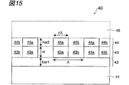
回折格子素子の第3参考形態について説明する。図15は、第3参考形態に係る回折格子素子40の説明図である。この図は、格子に垂直な面で切断したときの回折格子素子40の断面を示している。この図に示される回折格子素子40は、ベース板41、第1の反射抑制部42、回折格子部43、及び第2の反射抑制部44を備えて構成されている。
A third reference embodiment of the diffraction grating element will be described. FIG. 15 is an explanatory diagram of the
この回折格子素子40では、ベース板41上に第1の反射抑制部42が設けられており、第1の反射抑制部42上に回折格子部43が設けられており、回折格子部43上に第2の反射抑制部44が設けられている。第2の反射抑制部44は、第1媒質45に接している。回折格子部43では、ベース板41に実質的に平行な所定方向において第2媒質43aと第3媒質43bとが交互に設けられることによって回折格子が形成されている。第2の反射抑制部44においては、第2媒質43a上に媒質44a、第3媒質43b上に媒質44bが設けられている。この回折格子素子40は、反射率が10%以下となるように設計されたものである。
In this diffraction
この回折格子素子40では、第1媒質45から回折格子へ入射した光は、第2の反射抑制部44を経て、回折格子部43において回折され、第1の反射抑制部42を経て、ベース板41へ出射される。或いは、ベース板41から第1の反射抑制部42を経て回折格子へ入射した光は、回折格子部43において回折され、第2の反射抑制部44を経て、第1媒質45へ出射される。
In this diffraction
ここで回折格子部43は、以下のように定義される。すなわち、第2媒質43a及び第3媒質43bが交互に設けられた方向をx方向とし、第1の反射抑制部42、回折格子部43、及び第2の反射抑制部44が順に並ぶ方向をz方向とし、回折格子の周期をΛとし、周期Λにおける第2媒質43aが占める割合(デューティ比)をf、z方向における第1の反射抑制部42の長さ(すなわち、第1の反射抑制部42の高さ)をhar1、z方向における第2の反射抑制部44の長さ(すなわち、第2の反射抑制部44の高さ)をhar2、z方向における回折格子部43の長さ(すなわち、格子の高さ)をHとする。
Here, the diffraction
そして、平均屈折率nav(z)
![]()
![]()
回折格子素子40では、ベース板41が石英ガラス(屈折率:1.444)、回折格子部43の第2媒質43aがTa2O5(屈折率:2.107)、第2の反射抑制部44の媒質44aがSiO2、第1媒質45,第3媒質43b,及び媒質44bが空気(屈折率:1)であるものとして、RCWA法により回折格子部43のf,Hが設計され、以下に述べる等価モデルによる解析法で反射抑制部のhar1、har2が設計されている。
In the
等価モデルによる解析法とは、第1の反射抑制部42、回折格子部43、第2の反射抑制部44のそれぞれを、各々に含まれる媒質の平均屈折率をもつ単層膜と仮定し、かつ、回折格子部43での回折に伴う光の位相変化を90度と仮定し、回折格子素子40を多層膜に置き換えて、透過1次の回折効率、及び反射0次の回折効率を解析する方法である。この多層膜の透過率、反射率が、それぞれ回折格子素子40の透過1次回折効率、及び反射0次回折効率に相当する。よって、この等価モデルを用いることで、光学フィルタに代表される多層膜の設計理論が適用可能となり、回折格子素子40の反射0次回折効率の抑制設計が容易にできる。最終的に解析精度の高いRCWA法を用いて、回折格子素子40全体で、f,H,har1、har2の設計の微調整を行うとなお好適である。
The analysis method based on the equivalent model assumes that each of the first
図16は、第3参考形態に係る回折格子素子の反射0次回折効率と等価モデルの反射0次回折効率の特性を示すグラフである。このグラフは、周期Λ=1.0μm、f=0.579、H=1.164μm、har2=0.252μm、har1=−0.2μm、光の波長帯が1550nm帯(Cバンド帯)、光の入射角θ=50.58度の条件において、実際に製造された回折格子素子40と上記等価モデルの両者の反射0次回折効率の特性を示している。ここで、har1は負の値となっているが、この絶対値が第1の反射抑制部の厚みを表し、符号は後述のように反射抑制部の構造を表している。図16において、実線で示される特性は実際に製造された回折格子素子40によるものであり、点線で示される特性は上記等価モデルを用いた解析結果によるものである。このグラフから明確なように、中心波長に微小な差があるものの、この等価モデルを用いた設計方法によれば、本参考形態の回折格子素子40の特性を正確に得ることができる。
FIG. 16 is a graph showing the characteristics of the reflection zero-order diffraction efficiency of the diffraction grating element according to the third reference embodiment and the reflection zero-order diffraction efficiency of the equivalent model. This graph shows a period Λ = 1.0 μm, f = 0.579, H = 1.164 μm, h ar2 = 0.252 μm, h ar1 = −0.2 μm, and a light wavelength band of 1550 nm band (C band band). The graph shows the characteristics of the reflection zero-order diffraction efficiency of both the actually manufactured diffraction
回折格子素子40は、上記の等価モデルを用いた設計方法を用い、f,H,har1,har2の最適化が行われることによって設計されている。この設計においては、光の波長帯が1550nm帯(Cバンド帯)、光の入射角θ=50.58度の条件において、har1が−0.5μm〜0.3μmの範囲(0.1μm間隔)で最適化が行われている。
The
ここで、har1が正であることは、第1の反射抑制部42が、回折格子部43の媒質43aと同じ媒質によって構成されていることを示す。また、har1が負であることは、第1の反射抑制部42が、ベース板41の媒質と同じ媒質によって構成されていることを示す。図17は、参考例4の回折格子素子40Aの説明図であり、図18は、参考例5の回折格子素子40Bの説明図である。図17及び図18は共に、格子に垂直な面で切断した場合の回折格子素子の断面を示している。
Here, har1 being positive indicates that the first
回折格子素子40Aは、har1が正の場合の第3参考形態の回折格子素子40の例である。回折格子素子40Bは、har1が負の場合の第3参考形態の回折格子素子40の例である。回折格子素子40Aは、例えば、ベース板41上の一面に設けられた第2媒質43aをエッチングし、当該エッチングをベース板41に到達する前に停止させた場合に製造される。したがって、第2媒質43aと同一の媒質が第1の反射抑制部42を構成している。
The diffraction
一方、回折格子素子40Bは、har1が負の場合の第3参考形態の回折格子素子40の例である。回折格子素子40Bは、例えば、ベース板41上の一面に設けられた第2媒質43aをエッチングし、ベース板41の一部が削られるまで当該エッチングを行った場合に製造される。したがって、回折格子素子40Bは、交互に設けられた媒質42aと媒質42bとによって構成されており、媒質42aはベース板41と同一の媒質であり、媒質42bは空気となっている。
On the other hand, the diffraction
上記最適化の結果を表1、及び図19〜図21に示す。
図19は、第3参考形態に係る回折格子素子の回折効率を示すグラフである。図19は、表1に示す最小回折効率及び最大回折効率をそれぞれプロットしたものである。ここで、最大回折効率,最小回折効率とは、TE偏波光およびTM偏波光を含めて、Cバンド帯で最大の回折効率と最小の回折効率を示している。表1及び図19によれば、回折格子素子40は、90%以上の回折効率を有し、偏波依存性が小さいことがわかる。なお、上記実施形態並びに第1及び第2参考形態では、第2媒質及び第3媒質からなる回折格子部の上下にAR層、すなわち、回折格子部の外側の媒質と回折格子部との屈折率の差を吸収する層が設けられることによって、反射戻り光が抑制されている。これに対して、回折格子素子40の反射抑制部は上記実施形態並びに第1及び第2参考形態におけるAR層とは異なる条件の平均屈折率を有している。しかしながら、第1の反射抑制部42、回折格子部43、第2の反射抑制部44の多層膜によってベース板41と第1媒質45間のAR層が構成されることによって、回折格子素子40全体としての反射が抑制されている。
FIG. 19 is a graph showing the diffraction efficiency of the diffraction grating element according to the third reference embodiment. FIG. 19 is a plot of the minimum diffraction efficiency and the maximum diffraction efficiency shown in Table 1. Here, the maximum diffraction efficiency and the minimum diffraction efficiency indicate the maximum diffraction efficiency and the minimum diffraction efficiency in the C-band including TE polarized light and TM polarized light. According to Table 1 and FIG. 19, it can be seen that the
図20は、第3参考形態に係る回折格子素子における回折格子部のアスペクト比を示すグラフである。図20によれば、har1が−0.2μmまたは0.1μmの場合に、特にアスペクト比が小さいので、回折格子部43の製造が容易であることがわかる
FIG. 20 is a graph showing the aspect ratio of the diffraction grating portion in the diffraction grating element according to the third reference embodiment. According to Figure 20, when h ar1 is -0.2μm or 0.1 [mu] m, in particular because the aspect ratio is small, it can be seen that it is easy to manufacture the diffraction
図21は、第3参考形態に係る回折格子素子の溝深さトレランスを示すグラフである。ここで、溝深さトレランスとは、回折効率の変化を1%許容した場合にのhar1の変化の許容値、すなわち、溝深さ誤差を示している。図21によれば、har1が約−0.2μmの場合に溝深さ誤差の許容値が大きく、回折格子素子40の製造が容易であることがわかる。
FIG. 21 is a graph showing the groove depth tolerance of the diffraction grating element according to the third embodiment. Here, the groove depth tolerance indicates an allowable value of change in har1 when a change in diffraction efficiency is allowed 1%, that is, a groove depth error. According to FIG. 21, large tolerance of groove depth error when h ar1 is about -0.2, it can be seen that it is easy to manufacture the
(変形例) (Modification)
本発明は、上記実施形態に限定されるものではなく、種々の変形が可能である。例えば、回折格子部を形成する第2媒質および第3媒質の各領域の断面形状は、上記の実施形態では長方形であるとしたが、必ずしも長方形である必要はなく、例えば台形であってもよい。デューティ比f,f5およびf6は、上記の実施例では等しいとしたが、互いに異なっていてもよく、後者のようにすることにより回折特性が更に向上し得る。また、実施形態の回折格子素子において、第1媒質の側から光が入射してもよいし、第4媒質の側から光が入射してもよい。 The present invention is not limited to the above embodiment, and various modifications can be made. For example, the cross-sectional shape of each region of the second medium and the third medium forming the diffraction grating portion is a rectangle in the above embodiment , but it is not necessarily a rectangle, and may be a trapezoid, for example. . The duty ratios f, f 5 and f 6 are equal in the above embodiment , but may be different from each other, and the diffraction characteristics can be further improved by using the latter. In the diffraction grating element of the embodiment , light may be incident from the first medium side or light may be incident from the fourth medium side.
また、上記実施形態においては、第2媒質と第3媒質が互いに接し、かつ、交互に設けられることによって、回折格子部が形成されているが、第2媒質と第3媒質との間に異なる媒質が設けられていても良い。かかる態様を、第2参考形態の参考例3に係る回折格子素子30Aの変形態様を例として説明する。図22は、変形態様に係る回折格子素子の説明図である。図22は、格子に垂直な面で切断したときの回折格子素子の断面を示している。図22に示す回折格子素子30Bは、回折格子素子30Aと同様の構成を有し、第2媒質32と第3媒質33との間に、媒質36が設けられている。例えば、媒質35aがSiO2によって構成されており、エッチング時の媒質35aの側面の削れを補うために、第2媒質32のエッチング時にSiO2を付着させるプロセスを導入した場合には、媒質36がSiO2によって構成される回折格子素子30Bが製造される。また、第2媒質32がTa2O5によって構成されており、エッチング時の第2媒質32の側面の削れを補うために、第2媒質32のエッチング時にTa2O5を付着させるプロセスを導入した場合には、媒質36がTa2O5によって構成される回折格子素子30Bが製造される。
Moreover, in the said embodiment, although a 2nd medium and a 3rd medium mutually contact and are provided alternately, the diffraction grating part is formed, but it differs between a 2nd medium and a 3rd medium. A medium may be provided. Such a mode will be described by taking a modified mode of the diffraction
実施例は、波長帯域1.5μm〜1.6μmで設計を行なったものであるが、これに限定されるものではない。回折格子の設計では、相似則が成立するので、例えば中心波長を1.55μmから1.3μmに変更する場合、長さの単位を持つ設計パラメータ(周期や厚み)を全て1.3/1.55倍にすればよい。このようにして、光通信で用いられる波長帯域1.26μm〜1.675μm内の何れかの波長を中心波長とした回折格子を容易に設計することができる。 The embodiment is designed in the wavelength band of 1.5 μm to 1.6 μm, but is not limited to this. In the design of a diffraction grating, a similarity rule is established, and therefore, for example, when the center wavelength is changed from 1.55 μm to 1.3 μm, all design parameters (period and thickness) having a unit of length are 1.3 / 1. What is necessary is just to make it 55 times. In this way, it is possible to easily design a diffraction grating whose center wavelength is any wavelength within the wavelength band of 1.26 μm to 1.675 μm used in optical communication.
以上、詳細に説明したとおり、本発明によれば、回折効率の向上および回折効率の偏波依存性の低減を広い波長域で実現することができる。 As described above in detail, according to the present invention, it is possible to improve the diffraction efficiency and reduce the polarization dependence of the diffraction efficiency in a wide wavelength range.
Claims (11)
平面を有する第1媒質(屈折率n1)と、
前記第1媒質の前記平面に平行な平面を有する第4媒質(屈折率n4)と、
前記第1媒質の前記平面と前記第4媒質の前記平面との間において、前記第1媒質の前記平面および前記第4媒質の前記平面に接して、前記第1媒質の前記平面に平行な所定方向に交互に設けられて回折格子を形成している第2媒質(屈折率n2)および第3媒質(屈折率n3、ただし、n3<n2)と、
を備え、
前記第1媒質、前記第2媒質、前記第3媒質および前記第4媒質それぞれの屈折率n1〜n4が「n3<n1<n2、n3≦n4≦n2」または「n3≦n1≦n2、n3<n4<n2」なる関係式を満たし、
前記第2媒質および前記第3媒質の双方が固体であり、
前記第1媒質の前記平面と前記第4媒質の前記平面との間における平均屈折率をn av としたときに、前記第1媒質の屈折率n 1 が「n av −0.2≦n 1 ≦n av +0.2」なる関係式を満たし、
前記第4媒質の屈折率n 4 が「n av −0.2≦n 4 ≦n av +0.2」なる関係式を満たし、
前記第2媒質の屈折率n 2 と前記第3媒質の屈折率n 3 との差が0.7以上である、
回折格子素子。A transmission type diffraction grating element that demultiplexes or multiplexes light including a plurality of wavelengths,
A first medium having a plane (refractive index n 1 );
A fourth medium (refractive index n 4 ) having a plane parallel to the plane of the first medium;
A predetermined plane parallel to the plane of the first medium in contact with the plane of the first medium and the plane of the fourth medium between the plane of the first medium and the plane of the fourth medium. A second medium (refractive index n 2 ) and a third medium (refractive index n 3 , where n 3 <n 2 ) alternately provided in the direction to form a diffraction grating;
With
Refractive indexes n 1 to n 4 of the first medium, the second medium, the third medium, and the fourth medium are “n 3 <n 1 <n 2 , n 3 ≦ n 4 ≦ n 2 ” or “ n 3 ≦ n 1 ≦ n 2 , n 3 <n 4 <n 2 ”is satisfied,
Ri both solid der of the second medium and the third medium,
When the average refractive index between the plane of the first medium and the plane of the fourth medium is n av , the refractive index n 1 of the first medium is “n av −0.2 ≦ n 1. ≦ n av +0.2 ”is satisfied,
The refractive index n 4 of the fourth medium satisfies the relational expression “n av −0.2 ≦ n 4 ≦ n av +0.2”,
The difference between the refractive index n 3 of the third medium and the refractive index n 2 of the second medium is 0.7 or more,
Diffraction grating element.
平面を有する第1媒質(屈折率n1)と、
前記第1媒質の前記平面に平行な平面を有する第4媒質(屈折率n4)と、
前記第1媒質の前記平面と前記第4媒質の前記平面との間に、前記第1媒質の前記平面および前記第4媒質の前記平面に接して、前記第1媒質の前記平面に平行な所定方向に交互に設けられて回折格子を形成している第2媒質(屈折率n2)および第3媒質(屈折率n3、ただし、n3<n2)と、
を備え、
前記第1媒質、前記第2媒質、前記第3媒質および前記第4媒質それぞれの屈折率n1〜n4が「n3<n1<n2、n3≦n4≦n2」または「n3≦n1≦n2、n3<n4<n2」なる関係式を満たし、
前記第1媒質または前記第4媒質が等方性材料からなり、
前記第1媒質の前記平面と前記第4媒質の前記平面との間における平均屈折率をnavとしたときに、前記第1媒質の屈折率n1が「nav−0.2≦n1≦nav+0.2」なる関係式を満たし、
前記第4媒質の屈折率n 4 が「n av −0.2≦n 4 ≦n av +0.2」なる関係式を満たし、
前記第2媒質の屈折率n 2 と前記第3媒質の屈折率n 3 との差が0.7以上である、
回折格子素子。A transmission type diffraction grating element that demultiplexes or multiplexes light including a plurality of wavelengths,
A first medium having a plane (refractive index n 1 );
A fourth medium (refractive index n 4 ) having a plane parallel to the plane of the first medium;
A predetermined plane parallel to the plane of the first medium in contact with the plane of the first medium and the plane of the fourth medium between the plane of the first medium and the plane of the fourth medium. A second medium (refractive index n 2 ) and a third medium (refractive index n 3 , where n 3 <n 2 ) alternately provided in the direction to form a diffraction grating;
With
Refractive indexes n 1 to n 4 of the first medium, the second medium, the third medium, and the fourth medium are “n 3 <n 1 <n 2 , n 3 ≦ n 4 ≦ n 2 ” or “ n 3 ≦ n 1 ≦ n 2 , n 3 <n 4 <n 2 ”is satisfied,
Ri Do from the first medium or the fourth medium isotropic material,
When the average refractive index between the plane of the first medium and the plane of the fourth medium is nav, the refractive index n1 of the first medium is “nav−0.2 ≦ n1 ≦ nav + 0.2”. Is satisfied,
The refractive index n 4 of the fourth medium satisfies the relational expression “n av −0.2 ≦ n 4 ≦ n av +0.2”,
The difference between the refractive index n 3 of the third medium and the refractive index n 2 of the second medium is 0.7 or more,
Diffraction grating element.
Applications Claiming Priority (3)
| Application Number | Priority Date | Filing Date | Title |
|---|---|---|---|
| JP2003040196 | 2003-02-18 | ||
| JP2003040196 | 2003-02-18 | ||
| PCT/JP2004/000686 WO2004074888A1 (en) | 2003-02-18 | 2004-01-27 | Diffraction lattice element, production method for diffraction lattice element, and design method for diffraction lattice element |
Related Child Applications (3)
| Application Number | Title | Priority Date | Filing Date |
|---|---|---|---|
| JP2009089446A Division JP4600578B2 (en) | 2003-02-18 | 2009-04-01 | Diffraction grating element |
| JP2009089432A Division JP4600577B2 (en) | 2003-02-18 | 2009-04-01 | Diffraction grating element |
| JP2009089448A Division JP4600579B2 (en) | 2003-02-18 | 2009-04-01 | Diffraction grating element |
Publications (2)
| Publication Number | Publication Date |
|---|---|
| JPWO2004074888A1 JPWO2004074888A1 (en) | 2006-06-01 |
| JP4609318B2 true JP4609318B2 (en) | 2011-01-12 |
Family
ID=32905208
Family Applications (4)
| Application Number | Title | Priority Date | Filing Date |
|---|---|---|---|
| JP2005502667A Expired - Lifetime JP4609318B2 (en) | 2003-02-18 | 2004-01-27 | Diffraction grating element |
| JP2009089446A Expired - Lifetime JP4600578B2 (en) | 2003-02-18 | 2009-04-01 | Diffraction grating element |
| JP2009089448A Expired - Lifetime JP4600579B2 (en) | 2003-02-18 | 2009-04-01 | Diffraction grating element |
| JP2009089432A Expired - Lifetime JP4600577B2 (en) | 2003-02-18 | 2009-04-01 | Diffraction grating element |
Family Applications After (3)
| Application Number | Title | Priority Date | Filing Date |
|---|---|---|---|
| JP2009089446A Expired - Lifetime JP4600578B2 (en) | 2003-02-18 | 2009-04-01 | Diffraction grating element |
| JP2009089448A Expired - Lifetime JP4600579B2 (en) | 2003-02-18 | 2009-04-01 | Diffraction grating element |
| JP2009089432A Expired - Lifetime JP4600577B2 (en) | 2003-02-18 | 2009-04-01 | Diffraction grating element |
Country Status (6)
| Country | Link |
|---|---|
| EP (2) | EP2214037B1 (en) |
| JP (4) | JP4609318B2 (en) |
| CN (4) | CN100338486C (en) |
| CA (5) | CA2703171C (en) |
| DK (2) | DK1596226T3 (en) |
| WO (1) | WO2004074888A1 (en) |
Families Citing this family (22)
| Publication number | Priority date | Publication date | Assignee | Title |
|---|---|---|---|---|
| WO2004081620A1 (en) | 2003-03-13 | 2004-09-23 | Asahi Glass Company Limited | Diffraction element and optical device |
| US7420735B2 (en) * | 2004-07-26 | 2008-09-02 | Nippon Sheet Glass Co., Ltd. | Transmission type diffraction grating |
| JP4759973B2 (en) * | 2004-10-18 | 2011-08-31 | 日立電線株式会社 | Demultiplexer and wavelength division multiplexing optical transmission module |
| JP2006350126A (en) * | 2005-06-17 | 2006-12-28 | Sharp Corp | Wavelength selection element |
| JP2007101926A (en) * | 2005-10-05 | 2007-04-19 | Nippon Sheet Glass Co Ltd | Transmission grating and spectral element and spectroscope using the same |
| JP4908838B2 (en) * | 2005-12-13 | 2012-04-04 | 富士通株式会社 | Multi-wavelength spectrometer |
| JP5280654B2 (en) * | 2006-09-21 | 2013-09-04 | 日本板硝子株式会社 | Transmission diffraction grating, and spectroscopic element and spectroscope using the same |
| CA2600900A1 (en) | 2006-09-21 | 2008-03-21 | Nippon Sheet Glass Company, Limited | Transmissive diffraction grating, and spectral separation element and spectroscope using the same |
| JP5146317B2 (en) * | 2006-10-10 | 2013-02-20 | 旭硝子株式会社 | Diffraction element and optical head device provided with the same |
| TW200913238A (en) | 2007-06-04 | 2009-03-16 | Sony Corp | Optical member, solid state imaging apparatus, and manufacturing method |
| FR2954524B1 (en) * | 2009-12-17 | 2012-09-28 | Ecole Polytech | OPTIMIZED DIELECTRIC REFLECTING DIFFRACTION NETWORK |
| JP5724213B2 (en) * | 2010-05-13 | 2015-05-27 | セイコーエプソン株式会社 | Detection device |
| WO2013096974A1 (en) * | 2011-12-21 | 2013-06-27 | THE UNITED STATES OF AMERICA, as represented by THE SECRETARY DEPT. OF HEALTH AND HUMAN SERVICES | Multilayer-coated micro grating array for x-ray phase sensitive and scattering sensitive imaging |
| JP6007830B2 (en) | 2012-03-26 | 2016-10-12 | 旭硝子株式会社 | Transmission diffraction element |
| CN103645530B (en) * | 2013-11-06 | 2016-03-02 | 中国科学院物理研究所 | Reflection type optical element and method for designing thereof and application in solar cells |
| CN108761610A (en) * | 2018-06-13 | 2018-11-06 | 成都精密光学工程研究中心 | Regulate and control the unrelated reflective dielectric grating of polarization of film based on refractive index |
| CN108917927B (en) * | 2018-07-27 | 2020-08-25 | 京东方科技集团股份有限公司 | Dispersion device and spectrometer |
| CN109343163B (en) * | 2018-12-06 | 2021-04-20 | 深圳大学 | Manufacturing method of simple-period grating structure and terahertz filter |
| EP3671310A1 (en) * | 2018-12-18 | 2020-06-24 | Thomson Licensing | Optical manipulation apparatus for trapping or moving micro or nanoparticles |
| US11256012B2 (en) | 2019-02-27 | 2022-02-22 | Boe Technology Group Co., Ltd. | Color dispersion apparatus and spectrometer |
| CN113161463B (en) * | 2021-03-01 | 2023-04-07 | 武汉光迅科技股份有限公司 | Inclined cavity chip structure |
| CN116338856B (en) * | 2023-04-19 | 2023-09-29 | 嘉兴驭光光电科技有限公司 | Optical waveguide device for display and display apparatus having the same |
Family Cites Families (16)
| Publication number | Priority date | Publication date | Assignee | Title |
|---|---|---|---|---|
| US4484797A (en) * | 1981-07-20 | 1984-11-27 | Rca Corporation | Diffractive subtractive color filter responsive to angle of incidence of polychromatic illuminating light |
| DE3412958A1 (en) * | 1984-04-06 | 1985-10-17 | Dr. Johannes Heidenhain Gmbh, 8225 Traunreut | Phase grating |
| JPS63109402A (en) * | 1986-10-27 | 1988-05-14 | Sharp Corp | Preparation of optical phase operating plate |
| JP3199829B2 (en) * | 1992-03-26 | 2001-08-20 | 株式会社半導体エネルギー研究所 | Manufacturing method of amorphous carbon film |
| US5598300A (en) | 1995-06-05 | 1997-01-28 | Board Of Regents, The University Of Texas System | Efficient bandpass reflection and transmission filters with low sidebands based on guided-mode resonance effects |
| US5728456A (en) * | 1996-02-01 | 1998-03-17 | Optical Coating Laboratory, Inc. | Methods and apparatus for providing an absorbing, broad band, low brightness, antireflection coating |
| IL118209A0 (en) * | 1996-05-09 | 1998-02-08 | Yeda Res & Dev | Active electro-optical wavelength-selective mirrors and active electro-optic wavelength-selective filters |
| JPH1010306A (en) * | 1996-06-24 | 1998-01-16 | Matsushita Electric Ind Co Ltd | Artificial lattice and formation of artificial lattice |
| US6233381B1 (en) * | 1997-07-25 | 2001-05-15 | Corning Incorporated | Photoinduced grating in oxynitride glass |
| JP2000137109A (en) * | 1998-10-30 | 2000-05-16 | Shimadzu Corp | Reflection preventive device using diffraction grating |
| US6365428B1 (en) * | 2000-06-15 | 2002-04-02 | Sandia Corporation | Embedded high-contrast distributed grating structures |
| CA2387716A1 (en) * | 2000-08-29 | 2002-03-07 | Jsr Corporation | Radiation sensitive refractive index changing composition and refractive index changing method |
| JP2002182003A (en) * | 2000-12-14 | 2002-06-26 | Canon Inc | Antireflection functional element, optical element, optical system and optical appliance |
| US6762880B2 (en) * | 2001-02-21 | 2004-07-13 | Ibsen Photonics A/S | Grating structures and methods of making the grating structures |
| JP3711446B2 (en) * | 2001-03-05 | 2005-11-02 | 独立行政法人科学技術振興機構 | Wavelength filter |
| JP2003014914A (en) * | 2001-07-02 | 2003-01-15 | Sharp Corp | Diffraction element and optical pickup device assembled with the same |
-
2004
- 2004-01-27 CN CNB2004800001206A patent/CN100338486C/en not_active Expired - Lifetime
- 2004-01-27 WO PCT/JP2004/000686 patent/WO2004074888A1/en active Application Filing
- 2004-01-27 CN CNB2007101417036A patent/CN100526918C/en not_active Expired - Lifetime
- 2004-01-27 CA CA2703171A patent/CA2703171C/en not_active Expired - Lifetime
- 2004-01-27 DK DK04705514.0T patent/DK1596226T3/en active
- 2004-01-27 CA CA2703119A patent/CA2703119C/en not_active Expired - Lifetime
- 2004-01-27 DK DK10160274.6T patent/DK2214037T3/en active
- 2004-01-27 CA CA2703098A patent/CA2703098C/en not_active Expired - Lifetime
- 2004-01-27 CA CA2702951A patent/CA2702951C/en not_active Expired - Lifetime
- 2004-01-27 CN CNB2007101417040A patent/CN100526919C/en not_active Expired - Lifetime
- 2004-01-27 CA CA2480350A patent/CA2480350C/en not_active Expired - Lifetime
- 2004-01-27 EP EP10160274A patent/EP2214037B1/en not_active Expired - Lifetime
- 2004-01-27 CN CNB2007101417021A patent/CN100485424C/en not_active Expired - Lifetime
- 2004-01-27 EP EP04705514A patent/EP1596226B1/en not_active Expired - Lifetime
- 2004-01-27 JP JP2005502667A patent/JP4609318B2/en not_active Expired - Lifetime
-
2009
- 2009-04-01 JP JP2009089446A patent/JP4600578B2/en not_active Expired - Lifetime
- 2009-04-01 JP JP2009089448A patent/JP4600579B2/en not_active Expired - Lifetime
- 2009-04-01 JP JP2009089432A patent/JP4600577B2/en not_active Expired - Lifetime
Also Published As
| Publication number | Publication date |
|---|---|
| JP2009187016A (en) | 2009-08-20 |
| CA2702951C (en) | 2012-01-10 |
| EP2214037B1 (en) | 2012-11-14 |
| CA2703098C (en) | 2012-01-24 |
| CA2480350A1 (en) | 2004-09-02 |
| EP1596226A1 (en) | 2005-11-16 |
| JP4600578B2 (en) | 2010-12-15 |
| EP1596226A4 (en) | 2009-09-02 |
| CA2480350C (en) | 2011-06-21 |
| CA2702951A1 (en) | 2004-09-02 |
| DK1596226T3 (en) | 2012-09-03 |
| JP4600577B2 (en) | 2010-12-15 |
| CN101114031A (en) | 2008-01-30 |
| CA2703119C (en) | 2012-08-14 |
| WO2004074888A1 (en) | 2004-09-02 |
| CN101114030A (en) | 2008-01-30 |
| CN100485424C (en) | 2009-05-06 |
| CA2703119A1 (en) | 2004-09-02 |
| CN100338486C (en) | 2007-09-19 |
| JPWO2004074888A1 (en) | 2006-06-01 |
| EP2214037A1 (en) | 2010-08-04 |
| JP4600579B2 (en) | 2010-12-15 |
| JP2009187018A (en) | 2009-08-20 |
| CN101114032A (en) | 2008-01-30 |
| EP1596226B1 (en) | 2012-06-13 |
| DK2214037T3 (en) | 2013-02-11 |
| CN1697986A (en) | 2005-11-16 |
| CA2703171C (en) | 2012-01-24 |
| CN100526919C (en) | 2009-08-12 |
| CA2703171A1 (en) | 2004-09-02 |
| CN100526918C (en) | 2009-08-12 |
| CA2703098A1 (en) | 2004-09-02 |
| JP2009187017A (en) | 2009-08-20 |
Similar Documents
| Publication | Publication Date | Title |
|---|---|---|
| JP4600578B2 (en) | Diffraction grating element | |
| US7184214B2 (en) | Diffraction grating element, production method of diffraction grating element, and method of designing diffraction grating element | |
| US8165436B2 (en) | Highly efficient optical gratings with reduced thickness requirements and impedance-matching layers | |
| US7379241B2 (en) | High efficiency phase grating having a planar reflector | |
| US7554734B1 (en) | Polarization independent grating | |
| JP5280654B2 (en) | Transmission diffraction grating, and spectroscopic element and spectroscope using the same | |
| JP2011138169A (en) | Transmission diffraction optical element | |
| US20100091369A1 (en) | Double-layer grating | |
| JP4369256B2 (en) | Spectroscopic optical element | |
| JP4749789B2 (en) | Transmission type diffractive optical element | |
| JP2007101926A (en) | Transmission grating and spectral element and spectroscope using the same | |
| JP4139420B2 (en) | Wavelength filter | |
| JP2008276074A (en) | Filter for optical communication, and module for optical communication using the same |
Legal Events
| Date | Code | Title | Description |
|---|---|---|---|
| A621 | Written request for application examination |
Free format text: JAPANESE INTERMEDIATE CODE: A621 Effective date: 20060510 |
|
| A131 | Notification of reasons for refusal |
Free format text: JAPANESE INTERMEDIATE CODE: A131 Effective date: 20090210 |
|
| A521 | Request for written amendment filed |
Free format text: JAPANESE INTERMEDIATE CODE: A523 Effective date: 20090401 |
|
| A131 | Notification of reasons for refusal |
Free format text: JAPANESE INTERMEDIATE CODE: A131 Effective date: 20100427 |
|
| A521 | Request for written amendment filed |
Free format text: JAPANESE INTERMEDIATE CODE: A523 Effective date: 20100622 |
|
| A131 | Notification of reasons for refusal |
Free format text: JAPANESE INTERMEDIATE CODE: A131 Effective date: 20100713 |
|
| A521 | Request for written amendment filed |
Free format text: JAPANESE INTERMEDIATE CODE: A523 Effective date: 20100729 |
|
| TRDD | Decision of grant or rejection written | ||
| A01 | Written decision to grant a patent or to grant a registration (utility model) |
Free format text: JAPANESE INTERMEDIATE CODE: A01 Effective date: 20100914 |
|
| A01 | Written decision to grant a patent or to grant a registration (utility model) |
Free format text: JAPANESE INTERMEDIATE CODE: A01 |
|
| A61 | First payment of annual fees (during grant procedure) |
Free format text: JAPANESE INTERMEDIATE CODE: A61 Effective date: 20100927 |
|
| FPAY | Renewal fee payment (event date is renewal date of database) |
Free format text: PAYMENT UNTIL: 20131022 Year of fee payment: 3 |
|
| R150 | Certificate of patent or registration of utility model |
Ref document number: 4609318 Country of ref document: JP Free format text: JAPANESE INTERMEDIATE CODE: R150 |
|
| R250 | Receipt of annual fees |
Free format text: JAPANESE INTERMEDIATE CODE: R250 |
|
| R250 | Receipt of annual fees |
Free format text: JAPANESE INTERMEDIATE CODE: R250 |
|
| R250 | Receipt of annual fees |
Free format text: JAPANESE INTERMEDIATE CODE: R250 |
|
| R250 | Receipt of annual fees |
Free format text: JAPANESE INTERMEDIATE CODE: R250 |
|
| R250 | Receipt of annual fees |
Free format text: JAPANESE INTERMEDIATE CODE: R250 |
|
| R250 | Receipt of annual fees |
Free format text: JAPANESE INTERMEDIATE CODE: R250 |
|
| R250 | Receipt of annual fees |
Free format text: JAPANESE INTERMEDIATE CODE: R250 |
|
| R250 | Receipt of annual fees |
Free format text: JAPANESE INTERMEDIATE CODE: R250 |
|
| R250 | Receipt of annual fees |
Free format text: JAPANESE INTERMEDIATE CODE: R250 |
|
| R250 | Receipt of annual fees |
Free format text: JAPANESE INTERMEDIATE CODE: R250 |
|
| EXPY | Cancellation because of completion of term |