EP3668078A1 - Kameramodul und herstellungsverfahren dafür und zugehöriges intelligentes endgerät - Google Patents
Kameramodul und herstellungsverfahren dafür und zugehöriges intelligentes endgerät Download PDFInfo
- Publication number
- EP3668078A1 EP3668078A1 EP18843308.0A EP18843308A EP3668078A1 EP 3668078 A1 EP3668078 A1 EP 3668078A1 EP 18843308 A EP18843308 A EP 18843308A EP 3668078 A1 EP3668078 A1 EP 3668078A1
- Authority
- EP
- European Patent Office
- Prior art keywords
- camera module
- circuit board
- module according
- indented
- photosensitive element
- Prior art date
- Legal status (The legal status is an assumption and is not a legal conclusion. Google has not performed a legal analysis and makes no representation as to the accuracy of the status listed.)
- Granted
Links
Images




Classifications
-
- H—ELECTRICITY
- H04—ELECTRIC COMMUNICATION TECHNIQUE
- H04N—PICTORIAL COMMUNICATION, e.g. TELEVISION
- H04N23/00—Cameras or camera modules comprising electronic image sensors; Control thereof
- H04N23/50—Constructional details
-
- H—ELECTRICITY
- H04—ELECTRIC COMMUNICATION TECHNIQUE
- H04N—PICTORIAL COMMUNICATION, e.g. TELEVISION
- H04N23/00—Cameras or camera modules comprising electronic image sensors; Control thereof
- H04N23/50—Constructional details
- H04N23/54—Mounting of pick-up tubes, electronic image sensors, deviation or focusing coils
-
- H—ELECTRICITY
- H04—ELECTRIC COMMUNICATION TECHNIQUE
- H04N—PICTORIAL COMMUNICATION, e.g. TELEVISION
- H04N23/00—Cameras or camera modules comprising electronic image sensors; Control thereof
- H04N23/57—Mechanical or electrical details of cameras or camera modules specially adapted for being embedded in other devices
-
- H—ELECTRICITY
- H04—ELECTRIC COMMUNICATION TECHNIQUE
- H04M—TELEPHONIC COMMUNICATION
- H04M1/00—Substation equipment, e.g. for use by subscribers
- H04M1/02—Constructional features of telephone sets
- H04M1/0202—Portable telephone sets, e.g. cordless phones, mobile phones or bar type handsets
- H04M1/026—Details of the structure or mounting of specific components
- H04M1/0264—Details of the structure or mounting of specific components for a camera module assembly
-
- H—ELECTRICITY
- H05—ELECTRIC TECHNIQUES NOT OTHERWISE PROVIDED FOR
- H05K—PRINTED CIRCUITS; CASINGS OR CONSTRUCTIONAL DETAILS OF ELECTRIC APPARATUS; MANUFACTURE OF ASSEMBLAGES OF ELECTRICAL COMPONENTS
- H05K1/00—Printed circuits
- H05K1/02—Details
-
- H—ELECTRICITY
- H05—ELECTRIC TECHNIQUES NOT OTHERWISE PROVIDED FOR
- H05K—PRINTED CIRCUITS; CASINGS OR CONSTRUCTIONAL DETAILS OF ELECTRIC APPARATUS; MANUFACTURE OF ASSEMBLAGES OF ELECTRICAL COMPONENTS
- H05K2201/00—Indexing scheme relating to printed circuits covered by H05K1/00
- H05K2201/10—Details of components or other objects attached to or integrated in a printed circuit board
- H05K2201/10007—Types of components
- H05K2201/10121—Optical component, e.g. opto-electronic component
Definitions
- the invention relates to technical field of camera modules and intelligent terminals.
- Full-screen mobile phones In recent years, full-screen mobile phones have become a foreseen mobile phone development trend.
- Full-screen mobile phones generally refer to mobile phones with a front screen ratio of more than 80%.
- the use of ultra-narrow border screens has obvious appearance advantages compared to ordinary mobile phones, and brings a more shocking visual experience to mobile phone users. It is foreseeable that many mobile phone manufacturers are willing to adopt a full-screen solution.
- the front camera module of the mobile phone must be arranged on the side of the mobile phone that is very close to the side frame, such as the top and bottom sides.
- the frame or the back shell is often curved.
- the height of the camera module cannot be reduced synchronously due to the structural and optical design requirements, so the bottom of the mobile phone module is getting closer to the back shell or the curved surface of the curved frame.
- the edge of the camera module near the side of the mobile phone frame or the back shell is sharp and protruded, and it will interfere with the phone frame or back shell during installation, which is not convenient to installation.
- the present application aims to provide a solution capable of overcoming at least one of the aforementioned disadvantages.
- a camera module including: a circuit board; a photosensitive element mounted on the circuit board; and a support body formed on the circuit board and surrounding the photosensitive element, and the support body extending toward the photosensitive element and contacting the photosensitive element; wherein, the support body and the circuit board are fixed together to form a combined body, the combined body has a side surface, the side surface includes an indented surface indented toward the direction of the photosensitive element, and one end of the indented surface is located on the bottom surface of the circuit board.
- the indented surface is a curved surface in a stepped shape.
- the indented surface is a curved surface in a multi stepped shape.
- the indented surface is an inclined surface.
- the indented surface is composed of only a surface located on the circuit board.
- the indented surface is composed of a surface located on the circuit board and a surface located on the support body.
- the indented surface crosses an interface between the circuit board and the support body.
- the indented surface has a first end located on a bottom surface of the circuit board, and the photosensitive element has a first side closest to the indented surface; wherein, in a direction parallel to the bottom surface of the circuit board, a distance from the first end to the first side is 0.35 mm or less.
- the indented surface has a first end located on a bottom surface of the circuit board, and the photosensitive element has a first side closest to the indented surface; wherein, in a direction parallel to the bottom surface of the circuit board, a distance from the first end to the first side is 0.05 mm or more.
- the indented surface has a first end located on a bottom surface of the circuit board, and the photosensitive element has a first side closest to the indented surface; wherein, in a direction parallel to the bottom surface of the circuit board, a distance from the first end to the first side is 0.05 mm-0.35 mm.
- the indented surface is formed by performing a removal process on the combined body.
- the indented surface is formed by cutting or grinding the combined body.
- the support body extends towards the photosensitive element and covers at least a part of an edge region of the photosensitive element.
- the edge region is a region outside of an imaging region of the photosensitive element.
- the edge region surrounds periphery of the imaging region.
- the camera module has a lead wire electrically connecting the photosensitive element and the circuit board, and the support body covers the lead wire.
- the indented surface has a first end located on a bottom surface of the circuit board, and the circuit board has a soldering point connected to the lead wire; wherein, in a direction parallel to the bottom surface of the circuit board, a distance from the first end to the soldering point is 0.35 mm or less.
- the indented surface has a first end located on a bottom surface of the circuit board, and the circuit board has a soldering point connected to the lead wire; wherein, in a direction parallel to the bottom surface of the circuit board, a distance from the first end to the soldering point is 0.05 mm or more.
- the indented surface has a first end located on a bottom surface of the circuit board, and the circuit board has a soldering point connected to the lead wire; wherein, in a direction parallel to the bottom surface of the circuit board, a distance from the first end to the soldering point is 0.05 mm-0.35 mm.
- the support body is formed by a molding process.
- the camera module further includes an optical assembly mounted on the support body.
- the optical assembly includes a lens.
- the optical assembly includes a lens and a filter element.
- a method for manufacturing a camera module including: mounting a photosensitive element on a circuit board; forming a support body surrounding the photosensitive element on the circuit board, and the support body extending toward the photosensitive element and contacting the photosensitive element to form a combined body including the support body and the circuit board; performing a removal process on the combined body so that a side surface of the combined body forms a indented surface indented toward the direction of the photosensitive element, wherein one end of the indented surface is located on a bottom surface of the circuit board; and mounting an optical assembly on the support body to produce the camera module.
- the combined body in the step of performing a removal process on the combined body, is cut to form the indented surface in a stepped shape or the indented surface in an inclined shape.
- the combined body in the step of performing a removal process on the combined body, is grinded to form the indented surface in an inclined shape.
- the combined body in the step of performing a removal process on the combined body, is cut from the bottom surface of the circuit board to form the indented surface.
- the step of performing a removal process on the combined body includes: making a groove in an edge region of the bottom surface of the circuit board, the edge region being an area other than a central region supporting the photosensitive element, the groove being formed having two side walls and a top surface connecting the two side walls; and aligning at any position on the top surface and cuting the combined body to form the side surface with the indented surface along a direction perpendicular to the bottom surface of the circuit board.
- the depth of the groov is greater than the thickness of the circuit board.
- the depth of the groove is equal to the thickness of the circuit board.
- the depth of the groov is smaller than the thickness of the circuit board.
- the support body in the step of forming a support body on the circuit board, is formed on the circuit board by a molding process.
- the support body in the step of forming a support body on the circuit board, the support body extends toward the photosensitive element and covers at least a part of the edge area of the photosensitive element.
- an intelligent terminal including a curved case and the above mentioned camera module; wherein, the side of the camera module having the indented surface is close to the a curved case.
- the intelligent terminal is a smart phone.
- the curved case is a curved back shell or a curved frame.
- the camera module is a front camera module of the smart phone.
- the side surface with the indented surface is close to the curved surface of the top or bottom of the curved back shell.
- the side surface with the indented surface is close to the curved surface of the curved frame.
- the expressions of the first, second, etc. are only used to distinguish one feature from another feature, and do not indicate any limitation on the feature. Therefore, without departing from the teachings of this application, the first subject discussed below may also be referred to as the second subject.
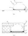
- Fig. 1 illustrates an embodiment of the camera module provided by the present application.
- the camera module 100 includes a circuit board 101, a photosensitive element 102, a support body 103, and an optical assembly 105.
- the circuit board 101 has a first surface and an opposite second surface, and the photosensitive element 102 is mounted on the first surface of the circuit board 101.
- the second surface serves as the bottom surface of the circuit board 101 (herein, the bottom surface of the circuit board refers to the second surface).
- the support body 103 is formed on the circuit board 101 and surrounds the photosensitive element 102, and the support body 103 extends toward the photosensitive element 102 and contacts the photosensitive element 102, so that there is no gap between the support body 103 and a side surface of the photosensitive element 102.
- the optical assembly 105 includes a lens and/or a color filter element. The optical assembly 105 is mounted on the supporting body 103 to form a complete camera module.
- the supporting body 103 is manufactured on the circuit board 101 by a molding process, and the supporting body 103 and the circuit board 101 are fixed together to form a combined body.
- the combined body has a side surface 104, the side surface 104 includes a indented surface 1041 indented toward the direction of the photosensitive element, and one end of the indented surface 1041 (for example, the first end 1048 shown in Fig. 1 ) is located on the bottom surface of the circuit board 101.
- the indented surface 1041 is a curved surface in a single-stepped state.
- the camera module 100 of this embodiment is particularly suitable for an intelligent terminal having an curved case. Since the camera module 100 has an indented surface 1041 near the edge of a side of the frame or the back shell of the intelligent terminal, the camera module 100 does not interfere with the frame or the back shell of the intelligent terminal when it is mounted. Thus, the curved frame or back shell of the intelligent terminal is closer, thereby further increasing the screen ratio of the intelligent terminal and allowing the thickness of the intelligent terminal to be further reduced.
- Fig. 2 is a schematic diagram showing the camera module 100 of the embodiment in Fig. 1 being mounted in an intelligent terminal 200 having a curved case.
- This drawing is a schematic partial cross-sectional view of the intelligent terminal 200 in a horizontally placed state, with the front of the intelligent terminal 200 facing up and the top on the right side.
- the camera module 100 is a front camera module, and the orientation of the lens is the same as that of the screen 202.
- the side surface 104 of the camera module 100 having the indented surface 1041 is close to the curved case 201, so that the camera module 100 can be as close to the top or bottom of the mobile phone as possible, thereby increasing the screen ratio.
- Fig. 3 is a schematic diagram showing a conventional camera module mounted in an intelligent terminal with a curved case. It can be seen that the side surface of the conventional camera module cannot be close to the curved case of the intelligent terminal, which makes it difficult to increase the screen ratio.
- Fig. 4 is a schematic diagram showing a comparison between an intelligent terminal (a lower side intelligent terminal) with a built-in camera module in the embodiment of Fig. 1 and an intelligent terminal (an upper side intelligent terminal) with a built-in conventional camera module. It can be seen that the camera module in the embodiment of Fig. 1 is closer to the curved case of the intelligent terminal than the conventional camera module, so that the mounting position of the camera module can be closer to the top of the intelligent terminal.
- Fig. 5 is a schematic diagram showing a comparison of screen ratios of an intelligent terminal (a right-side intelligent terminal) with a built-in camera module in the embodiment of Fig. 1 and an intelligent terminal (a left-side intelligent terminal) with a built-in conventional camera module. It can be seen that since the mounting position of the camera module is closer to the top of the intelligent terminal, the intelligent terminal with the built-in camera module in the embodiment of Fig. 1 increases the screen ratio.
- FIG. 6 is a schematic diagram showing a comparison between an intelligent terminal (a right-side intelligent terminal) with the built-in camera module of the embodiment in Fig. 1 and another intelligent terminal (a left-side intelligent terminal) with a built-in conventional camera module.
- the intelligent terminal the left-side intelligent terminal
- a side surface of the conventional camera module is close to the non-curved part of the case of the intelligent terminal, resulting in that the bottom surface of the circuit board cannot be close to or support the back shell of the intelligent terminal.
- the camera module in the embodiment of Fig. 1 can solve this problem well, thereby allowing the thickness of the intelligent terminal to be further reduced.
- the indented surface 1041 of the camera module in the embodiment of Fig. 1 uses a curved surface in a single-stepped state, but this shape is not unique.
- Fig. 7 is an enlarged schematic diagram showing a area near the indented surface 1041 in another embodiment of the present application.
- the indented surface 1041 is an inclined surface.
- the inclined surface can be obtained by cutting or grinding the circuit board 101. It is easy to think that the indented surface may also be a curved surface in a multi-stepped state.
- Fig. 8 to Fig. 10 are enlarged schematic diagrams showing the area near the indented surface 1041 in several other embodiments of the present application.
- the indented surface 1041 is a curved surface in a single-stepped state, and is composed of a surface 1042 on the circuit board 101 and a surface 1043 on the support body 103.
- the indented surface 1041 crosses the interface 106 between the circuit board 101 and the support body 103.
- the indented surface 1041 can be obtained by cutting the circuit board 101 and the support body 103.
- the indented surface 1041 is a curved surface in a single-stepped state, and is composed of only two surfaces 1044 and 1045 on the circuit board 101.
- the indented surface 1041 can be obtained by cutting the circuit board 101 and the support body 103.
- the indented surface 1041 is an inclined surface, and is composed of a surface 1046 on the circuit board 101 and a surface 1047 on the support body 103.
- the indented surface 1041 crosses the interface 106 between the circuit board 101 and the support body 103.
- the indented surface 1041 can be obtained by cutting or grinding the circuit board 101 and the supporting body 103.
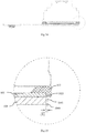
- Fig. 11 is an enlarged schematic diagram showing a area near a indented surface according to another embodiment of the present application.
- the camera module has a lead wire 107 (e.g., a gold wire) electrically connecting the photosensitive element 102 and the circuit board 101, and the support body 103 covers the lead wire 107 during molding.
- the indented surface 1041 has a first end 1048 on the bottom surface of the circuit board, and the circuit board 101 has a soldering point 1019 connected to the lead wire 107.
- a distance d1 between the first end 1048 and the soldering point 1019 may be preferably 0.05 mm-0.35 mm.
- this distance can better avoid the lead wire 107 (e.g., gold wires) and avoid damage to the camera module due to the manufacturing tolerances of the removal process.
- the indented surface can be used more fully to further improve the screen ratio of the intelligent terminal or reduce the thickness of the intelligent terminal.
- Fig. 12 is an enlarged schematic view showing the area near a side surface 304 of a combined body of a comparative embodiment.
- a conventional lens holder 303 is mounted on a circuit board 301 in an adhesive manner using a conventional dispensing process.
- a sufficient gap needs to be left between the conventional lens holder 303 and a photosensitive element 302.
- the conventional lens holder 303 needs to have a sufficient width d2 to provide support for other components (such as an optical assembly 305 or the circuit board 301) to prevent the camera module from deforming during manufacturing, mounting or usage, and it is also necessary to encapsulate the photosensitive element 302 to prevents dust from entering.
- the width d2 of the conventional lens holder 303 must not be too small, which results in a longer distance from the side surface 304 of the combined body to the photosensitive element 302, which is not beneficial for the miniaturization of the camera module and cannot achieve the effect of increasing the screen ratio of the intelligent terminal or reducing the thickness of the intelligent terminal.
- the supporting body 103 extends toward the photosensitive element 102 and covers at least a part of the edge region of the photosensitive element 102. Since there is no gap between the support body 103 and the photosensitive element 102, the side surface 104 of the combined body of the embodiment of Fig. 11 can be closer to the photosensitive element 102 compared to the comparative embodiment.
- the combined body can also be cut or grinded to form an indented surface 1041 indented toward the direction of the photosensitive element 102, thereby further achieving the effect of increasing the screen ratio of the intelligent terminal or reducing the thickness of the intelligent terminal.
- the camera module in the comparative embodiment it is difficult to cut or grind the combined body.
- Fig. 13 is a diagram showing an effect of cutting the camera module of the comparative embodiment of Fig. 12 . It can be seen that the cut camera module cannot be sealed, which may cause problems such as water leakage.
- Fig. 14 is a schematic diagram showing another embodiment of the present application.
- Fig. 15 is an enlarged view showing an area near an indented surface in the embodiment of Fig. 14 .
- there is no gold wire near the indented surface for embodiment, a lead wire is arranged on other side surface of the combined body, so that the area near the side surface including the indented surface is free of gold wire.
- the photosensitive element 102 has a first side 1021 closest to the indented surface 1041, and the indented surface 1041 has a first end 1048 located on a bottom surface of the circuit board 101.
- a distance d1 between the first end 1048 and the first side 1021 is 0.05 mm-0.35 mm.
- this distance can better avoid the photosensitive element 102 and avoid damage to the camera module due to the manufacturing tolerances of the removal process.
- the indented surface can be used more fully to further increase the screen ratio of the intelligent terminal or reduce the thickness of the intelligent terminal.
- Fig. 16 is a bottom view showing a camera module according to another embodiment of the present application.
- Fig. 17 is a schematic diagram showing an A-A cross section of the embodiment in Fig. 16.
- Fig. 18 is a schematic diagram showing a B-B cross section of the embodiment in Fig. 16 .
- a circuit board 401 and a supporting body 403 constitute a combined body, which includes a first side surface 404 having a first indented surface 4041 and a second side surface 405 having a second indented surface 4051.
- This design with two indented surfaces provided on both side surfaces can increase the screen ratio of the intelligent terminal and reduce the thickness of the intelligent terminal, while making the internal structure of the intelligent terminal more compact.
- the combined body may further have more side surfaces including an indented surface.
- the combined body may have three side surfaces including an indented surface.
- the edge region is a region outside of an imaging region of the photosensitive element. The edge region surrounds the imaging region.
- the combined body in the step 3, is cut to form the indented surface in a stepped state or the indented surface in an inclined surface state. Further, in an embodiment of the present application, in the step 3, the combined body is grinded to form the indented surface in an inclined surface state.
- step 3 the combined body is cut from the bottom surface of the circuit board to form the indented surface.
- the step 3 includes:
- the groove depth is equal to the thickness of the circuit board 101, so that the top surface 1016 is located at an interface between the support body 103 and the circuit board 101.
- the depth of the groove depth is smaller than the thickness of the circuit board 101, so that the top surface 1016 is located on the circuit board 101.
- step 2 when the support body is molded, the support body extends towards the photosensitive element and covers at least a part of the edge region of the photosensitive element.
- an intelligent terminal with a built-in camera module with an indented surface is also provided.
- the intelligent terminal includes a curved case and a camera module in any of the foregoing embodiments. Wherein, the side surface of the camera module having the indented surface is close to the curved case.
- the intelligent terminal may be a smart phone, or of course, other smart devices such as a tablet computer.
- the curved case may be a curved back shell or a curved frame.
- the camera module may be a front camera module of a smart phone.
- the side surface of the camera module having the indented surface is close to the curved surface of the top or bottom of the curved back shell. In another embodiment of the present application, the side surface with the indented surface is close to the curved surface of the curved frame.
Landscapes
- Engineering & Computer Science (AREA)
- Signal Processing (AREA)
- Multimedia (AREA)
- Microelectronics & Electronic Packaging (AREA)
- Camera Bodies And Camera Details Or Accessories (AREA)
- Studio Devices (AREA)
- Telephone Set Structure (AREA)
Priority Applications (1)
| Application Number | Priority Date | Filing Date | Title |
|---|---|---|---|
| EP22164915.5A EP4047920B1 (de) | 2017-08-07 | 2018-07-19 | Kameramodul, dessen herstellungsverfahren und entsprechendes intelligentes endgerät |
Applications Claiming Priority (3)
| Application Number | Priority Date | Filing Date | Title |
|---|---|---|---|
| CN201720978352.3U CN207304699U (zh) | 2017-08-07 | 2017-08-07 | 摄像模组以及相应的智能终端 |
| CN201710666721.XA CN107277336B (zh) | 2017-08-07 | 2017-08-07 | 摄像模组及其制作方法以及相应的智能终端 |
| PCT/CN2018/096307 WO2019029332A1 (zh) | 2017-08-07 | 2018-07-19 | 摄像模组及其制作方法以及相应的智能终端 |
Related Child Applications (2)
| Application Number | Title | Priority Date | Filing Date |
|---|---|---|---|
| EP22164915.5A Division-Into EP4047920B1 (de) | 2017-08-07 | 2018-07-19 | Kameramodul, dessen herstellungsverfahren und entsprechendes intelligentes endgerät |
| EP22164915.5A Division EP4047920B1 (de) | 2017-08-07 | 2018-07-19 | Kameramodul, dessen herstellungsverfahren und entsprechendes intelligentes endgerät |
Publications (3)
| Publication Number | Publication Date |
|---|---|
| EP3668078A4 EP3668078A4 (de) | 2020-06-17 |
| EP3668078A1 true EP3668078A1 (de) | 2020-06-17 |
| EP3668078B1 EP3668078B1 (de) | 2022-07-06 |
Family
ID=65273278
Family Applications (2)
| Application Number | Title | Priority Date | Filing Date |
|---|---|---|---|
| EP18843308.0A Active EP3668078B1 (de) | 2017-08-07 | 2018-07-19 | Kameramodul und zugehöriges herstellungsverfahren, und korrespondierendes intelligentes endgerät |
| EP22164915.5A Active EP4047920B1 (de) | 2017-08-07 | 2018-07-19 | Kameramodul, dessen herstellungsverfahren und entsprechendes intelligentes endgerät |
Family Applications After (1)
| Application Number | Title | Priority Date | Filing Date |
|---|---|---|---|
| EP22164915.5A Active EP4047920B1 (de) | 2017-08-07 | 2018-07-19 | Kameramodul, dessen herstellungsverfahren und entsprechendes intelligentes endgerät |
Country Status (5)
| Country | Link |
|---|---|
| US (1) | US11394861B2 (de) |
| EP (2) | EP3668078B1 (de) |
| JP (1) | JP6847300B2 (de) |
| KR (1) | KR102291793B1 (de) |
| WO (1) | WO2019029332A1 (de) |
Family Cites Families (21)
| Publication number | Priority date | Publication date | Assignee | Title |
|---|---|---|---|---|
| JP3782406B2 (ja) * | 2003-07-01 | 2006-06-07 | 松下電器産業株式会社 | 固体撮像装置およびその製造方法 |
| US7329861B2 (en) | 2003-10-14 | 2008-02-12 | Micron Technology, Inc. | Integrally packaged imaging module |
| KR101038492B1 (ko) * | 2004-08-31 | 2011-06-01 | 삼성테크윈 주식회사 | 카메라 모듈 및 그 제조 방법 |
| JP2007012995A (ja) * | 2005-07-01 | 2007-01-18 | Toshiba Corp | 超小型カメラモジュール及びその製造方法 |
| KR100770684B1 (ko) * | 2006-05-18 | 2007-10-29 | 삼성전기주식회사 | 카메라 모듈 패키지 |
| KR100813599B1 (ko) * | 2006-08-29 | 2008-03-17 | 삼성전기주식회사 | 칩 내장형 기판을 이용한 카메라 모듈 |
| KR20080079086A (ko) * | 2007-02-26 | 2008-08-29 | 삼성테크윈 주식회사 | 이미지 센서 모듈과 이를 구비한 카메라 모듈 및 그 제조방법 |
| JP2009025698A (ja) * | 2007-07-23 | 2009-02-05 | Konica Minolta Opto Inc | 撮像装置 |
| US7964945B2 (en) * | 2007-09-28 | 2011-06-21 | Samsung Electro-Mechanics Co., Ltd. | Glass cap molding package, manufacturing method thereof and camera module |
| JP5601000B2 (ja) | 2010-03-31 | 2014-10-08 | 株式会社リコー | 撮像装置 |
| JP2013101799A (ja) * | 2011-11-08 | 2013-05-23 | Smk Corp | 電子部品の基板接続構造 |
| CN203734738U (zh) * | 2014-02-28 | 2014-07-23 | 北京中科虹霸科技有限公司 | 一种用于移动终端的虹膜识别摄像头模组 |
| CN104767916A (zh) * | 2015-03-10 | 2015-07-08 | 南昌欧菲光电技术有限公司 | 摄像头模组 |
| CN104966724B (zh) * | 2015-06-15 | 2024-04-12 | 格科微电子(上海)有限公司 | 配置摄像头模组于终端主板的方法及终端设备 |
| CN105611135B (zh) | 2015-11-13 | 2019-03-19 | 宁波舜宇光电信息有限公司 | 系统级摄像模组及其电气支架和制造方法 |
| CN105554352A (zh) * | 2015-11-27 | 2016-05-04 | 小米科技有限责任公司 | 摄像头模组和电子设备 |
| CN106998415B (zh) * | 2016-01-25 | 2020-12-15 | Lg伊诺特有限公司 | 相机模块和光学设备 |
| CN206060925U (zh) * | 2016-04-20 | 2017-03-29 | 深圳市成像通科技有限公司 | 一种紧凑型摄像模组 |
| CN106131383A (zh) * | 2016-07-18 | 2016-11-16 | 信利光电股份有限公司 | 一种摄像模组及电子设备 |
| CN207304699U (zh) * | 2017-08-07 | 2018-05-01 | 宁波舜宇光电信息有限公司 | 摄像模组以及相应的智能终端 |
| CN107277336B (zh) * | 2017-08-07 | 2023-03-24 | 宁波舜宇光电信息有限公司 | 摄像模组及其制作方法以及相应的智能终端 |
-
2018
- 2018-07-19 WO PCT/CN2018/096307 patent/WO2019029332A1/zh not_active Ceased
- 2018-07-19 US US16/636,775 patent/US11394861B2/en active Active
- 2018-07-19 EP EP18843308.0A patent/EP3668078B1/de active Active
- 2018-07-19 JP JP2020506888A patent/JP6847300B2/ja active Active
- 2018-07-19 KR KR1020207006204A patent/KR102291793B1/ko active Active
- 2018-07-19 EP EP22164915.5A patent/EP4047920B1/de active Active
Also Published As
| Publication number | Publication date |
|---|---|
| US11394861B2 (en) | 2022-07-19 |
| JP2020530136A (ja) | 2020-10-15 |
| WO2019029332A1 (zh) | 2019-02-14 |
| EP3668078B1 (de) | 2022-07-06 |
| KR20200033327A (ko) | 2020-03-27 |
| EP4047920A1 (de) | 2022-08-24 |
| EP3668078A4 (de) | 2020-06-17 |
| KR102291793B1 (ko) | 2021-08-19 |
| JP6847300B2 (ja) | 2021-03-24 |
| EP4047920B1 (de) | 2024-08-28 |
| US20200382686A1 (en) | 2020-12-03 |
Similar Documents
| Publication | Publication Date | Title |
|---|---|---|
| US11785325B2 (en) | Camera module having circuit board, molded base, and optical lens, electronic device having same and method for manufacturing camera module | |
| CN107277336B (zh) | 摄像模组及其制作方法以及相应的智能终端 | |
| CN109683434B (zh) | 摄像模组阵列 | |
| US8190021B2 (en) | Smart phone with lens | |
| US10306032B2 (en) | Bracket assembly, camera module, and mobile terminal | |
| US20200382683A1 (en) | Array camera module and application thereof | |
| US11758253B2 (en) | Camera module having chamfer, photosensitive assembly, preparation method, and electronic device | |
| US11394861B2 (en) | Camera module, manufacturing method thereof and corresponding intelligent terminal | |
| US20220294941A1 (en) | Base, camera module and electronic device | |
| US20200304693A1 (en) | Camera module and electronic device using same | |
| CN115915745B (zh) | 显示模组及显示设备 | |
| TWI735084B (zh) | 複合座體、複合座體的製造方法、攝像頭模組及電子裝置 | |
| US11316278B2 (en) | Mobile terminal and glass housing thereof, and performance optimization method of antenna module thereof | |
| CN209897090U (zh) | 应用于移动终端的弯折显示玻璃 | |
| CN112596135A (zh) | 透镜、镜头模组及电子设备 | |
| CN110634960B (zh) | 感光组件、摄像模组及相应的终端设备和制作方法 | |
| CN214845970U (zh) | 一种镜头模组、成像装置及电子设备 | |
| US12308570B2 (en) | Electric connecting device | |
| US20260059730A1 (en) | Wireless communication device | |
| US20230327366A1 (en) | Electrical connector | |
| JP7335261B2 (ja) | 面取りを有する撮像モジュール、感光モジュールおよび電子機器 | |
| CN113126227A (zh) | 镜头模组、成像装置及电子设备 | |
| EP3291517B1 (de) | Anzeigebildschirmanordnung und mobiles endgerät | |
| TWM590803U (zh) | 具有雙重貼合片體之接地中板及其連接器 |
Legal Events
| Date | Code | Title | Description |
|---|---|---|---|
| STAA | Information on the status of an ep patent application or granted ep patent |
Free format text: STATUS: THE INTERNATIONAL PUBLICATION HAS BEEN MADE |
|
| PUAI | Public reference made under article 153(3) epc to a published international application that has entered the european phase |
Free format text: ORIGINAL CODE: 0009012 |
|
| STAA | Information on the status of an ep patent application or granted ep patent |
Free format text: STATUS: REQUEST FOR EXAMINATION WAS MADE |
|
| 17P | Request for examination filed |
Effective date: 20200227 |
|
| A4 | Supplementary search report drawn up and despatched |
Effective date: 20200520 |
|
| AK | Designated contracting states |
Kind code of ref document: A1 Designated state(s): AL AT BE BG CH CY CZ DE DK EE ES FI FR GB GR HR HU IE IS IT LI LT LU LV MC MK MT NL NO PL PT RO RS SE SI SK SM TR |
|
| AX | Request for extension of the european patent |
Extension state: BA ME |
|
| DAV | Request for validation of the european patent (deleted) | ||
| DAX | Request for extension of the european patent (deleted) | ||
| STAA | Information on the status of an ep patent application or granted ep patent |
Free format text: STATUS: EXAMINATION IS IN PROGRESS |
|
| 17Q | First examination report despatched |
Effective date: 20210414 |
|
| GRAP | Despatch of communication of intention to grant a patent |
Free format text: ORIGINAL CODE: EPIDOSNIGR1 |
|
| STAA | Information on the status of an ep patent application or granted ep patent |
Free format text: STATUS: GRANT OF PATENT IS INTENDED |
|
| INTG | Intention to grant announced |
Effective date: 20220127 |
|
| GRAS | Grant fee paid |
Free format text: ORIGINAL CODE: EPIDOSNIGR3 |
|
| GRAA | (expected) grant |
Free format text: ORIGINAL CODE: 0009210 |
|
| STAA | Information on the status of an ep patent application or granted ep patent |
Free format text: STATUS: THE PATENT HAS BEEN GRANTED |
|
| AK | Designated contracting states |
Kind code of ref document: B1 Designated state(s): AL AT BE BG CH CY CZ DE DK EE ES FI FR GB GR HR HU IE IS IT LI LT LU LV MC MK MT NL NO PL PT RO RS SE SI SK SM TR |
|
| REG | Reference to a national code |
Ref country code: AT Ref legal event code: REF Ref document number: 1503699 Country of ref document: AT Kind code of ref document: T Effective date: 20220715 Ref country code: CH Ref legal event code: EP |
|
| REG | Reference to a national code |
Ref country code: DE Ref legal event code: R096 Ref document number: 602018037725 Country of ref document: DE |
|
| REG | Reference to a national code |
Ref country code: IE Ref legal event code: FG4D |
|
| REG | Reference to a national code |
Ref country code: LT Ref legal event code: MG9D |
|
| REG | Reference to a national code |
Ref country code: NL Ref legal event code: MP Effective date: 20220706 |
|
| REG | Reference to a national code |
Ref country code: DE Ref legal event code: R079 Ref document number: 602018037725 Country of ref document: DE Free format text: PREVIOUS MAIN CLASS: H04N0005225000 Ipc: H04N0023000000 |
|
| PG25 | Lapsed in a contracting state [announced via postgrant information from national office to epo] |
Ref country code: SE Free format text: LAPSE BECAUSE OF FAILURE TO SUBMIT A TRANSLATION OF THE DESCRIPTION OR TO PAY THE FEE WITHIN THE PRESCRIBED TIME-LIMIT Effective date: 20220706 Ref country code: RS Free format text: LAPSE BECAUSE OF FAILURE TO SUBMIT A TRANSLATION OF THE DESCRIPTION OR TO PAY THE FEE WITHIN THE PRESCRIBED TIME-LIMIT Effective date: 20220706 Ref country code: PT Free format text: LAPSE BECAUSE OF FAILURE TO SUBMIT A TRANSLATION OF THE DESCRIPTION OR TO PAY THE FEE WITHIN THE PRESCRIBED TIME-LIMIT Effective date: 20221107 Ref country code: NO Free format text: LAPSE BECAUSE OF FAILURE TO SUBMIT A TRANSLATION OF THE DESCRIPTION OR TO PAY THE FEE WITHIN THE PRESCRIBED TIME-LIMIT Effective date: 20221006 Ref country code: NL Free format text: LAPSE BECAUSE OF FAILURE TO SUBMIT A TRANSLATION OF THE DESCRIPTION OR TO PAY THE FEE WITHIN THE PRESCRIBED TIME-LIMIT Effective date: 20220706 Ref country code: LV Free format text: LAPSE BECAUSE OF FAILURE TO SUBMIT A TRANSLATION OF THE DESCRIPTION OR TO PAY THE FEE WITHIN THE PRESCRIBED TIME-LIMIT Effective date: 20220706 Ref country code: LT Free format text: LAPSE BECAUSE OF FAILURE TO SUBMIT A TRANSLATION OF THE DESCRIPTION OR TO PAY THE FEE WITHIN THE PRESCRIBED TIME-LIMIT Effective date: 20220706 Ref country code: FI Free format text: LAPSE BECAUSE OF FAILURE TO SUBMIT A TRANSLATION OF THE DESCRIPTION OR TO PAY THE FEE WITHIN THE PRESCRIBED TIME-LIMIT Effective date: 20220706 Ref country code: ES Free format text: LAPSE BECAUSE OF FAILURE TO SUBMIT A TRANSLATION OF THE DESCRIPTION OR TO PAY THE FEE WITHIN THE PRESCRIBED TIME-LIMIT Effective date: 20220706 |
|
| REG | Reference to a national code |
Ref country code: AT Ref legal event code: MK05 Ref document number: 1503699 Country of ref document: AT Kind code of ref document: T Effective date: 20220706 |
|
| PG25 | Lapsed in a contracting state [announced via postgrant information from national office to epo] |
Ref country code: PL Free format text: LAPSE BECAUSE OF FAILURE TO SUBMIT A TRANSLATION OF THE DESCRIPTION OR TO PAY THE FEE WITHIN THE PRESCRIBED TIME-LIMIT Effective date: 20220706 Ref country code: IS Free format text: LAPSE BECAUSE OF FAILURE TO SUBMIT A TRANSLATION OF THE DESCRIPTION OR TO PAY THE FEE WITHIN THE PRESCRIBED TIME-LIMIT Effective date: 20221106 Ref country code: HR Free format text: LAPSE BECAUSE OF FAILURE TO SUBMIT A TRANSLATION OF THE DESCRIPTION OR TO PAY THE FEE WITHIN THE PRESCRIBED TIME-LIMIT Effective date: 20220706 Ref country code: GR Free format text: LAPSE BECAUSE OF FAILURE TO SUBMIT A TRANSLATION OF THE DESCRIPTION OR TO PAY THE FEE WITHIN THE PRESCRIBED TIME-LIMIT Effective date: 20221007 |
|
| REG | Reference to a national code |
Ref country code: CH Ref legal event code: PL |
|
| REG | Reference to a national code |
Ref country code: BE Ref legal event code: MM Effective date: 20220731 |
|
| REG | Reference to a national code |
Ref country code: DE Ref legal event code: R097 Ref document number: 602018037725 Country of ref document: DE |
|
| PG25 | Lapsed in a contracting state [announced via postgrant information from national office to epo] |
Ref country code: SM Free format text: LAPSE BECAUSE OF FAILURE TO SUBMIT A TRANSLATION OF THE DESCRIPTION OR TO PAY THE FEE WITHIN THE PRESCRIBED TIME-LIMIT Effective date: 20220706 Ref country code: RO Free format text: LAPSE BECAUSE OF FAILURE TO SUBMIT A TRANSLATION OF THE DESCRIPTION OR TO PAY THE FEE WITHIN THE PRESCRIBED TIME-LIMIT Effective date: 20220706 Ref country code: MC Free format text: LAPSE BECAUSE OF FAILURE TO SUBMIT A TRANSLATION OF THE DESCRIPTION OR TO PAY THE FEE WITHIN THE PRESCRIBED TIME-LIMIT Effective date: 20220706 Ref country code: LU Free format text: LAPSE BECAUSE OF NON-PAYMENT OF DUE FEES Effective date: 20220719 Ref country code: LI Free format text: LAPSE BECAUSE OF NON-PAYMENT OF DUE FEES Effective date: 20220731 Ref country code: DK Free format text: LAPSE BECAUSE OF FAILURE TO SUBMIT A TRANSLATION OF THE DESCRIPTION OR TO PAY THE FEE WITHIN THE PRESCRIBED TIME-LIMIT Effective date: 20220706 Ref country code: CZ Free format text: LAPSE BECAUSE OF FAILURE TO SUBMIT A TRANSLATION OF THE DESCRIPTION OR TO PAY THE FEE WITHIN THE PRESCRIBED TIME-LIMIT Effective date: 20220706 Ref country code: CH Free format text: LAPSE BECAUSE OF NON-PAYMENT OF DUE FEES Effective date: 20220731 Ref country code: AT Free format text: LAPSE BECAUSE OF FAILURE TO SUBMIT A TRANSLATION OF THE DESCRIPTION OR TO PAY THE FEE WITHIN THE PRESCRIBED TIME-LIMIT Effective date: 20220706 |
|
| PLBE | No opposition filed within time limit |
Free format text: ORIGINAL CODE: 0009261 |
|
| STAA | Information on the status of an ep patent application or granted ep patent |
Free format text: STATUS: NO OPPOSITION FILED WITHIN TIME LIMIT |
|
| PG25 | Lapsed in a contracting state [announced via postgrant information from national office to epo] |
Ref country code: SK Free format text: LAPSE BECAUSE OF FAILURE TO SUBMIT A TRANSLATION OF THE DESCRIPTION OR TO PAY THE FEE WITHIN THE PRESCRIBED TIME-LIMIT Effective date: 20220706 Ref country code: EE Free format text: LAPSE BECAUSE OF FAILURE TO SUBMIT A TRANSLATION OF THE DESCRIPTION OR TO PAY THE FEE WITHIN THE PRESCRIBED TIME-LIMIT Effective date: 20220706 Ref country code: BE Free format text: LAPSE BECAUSE OF NON-PAYMENT OF DUE FEES Effective date: 20220731 |
|
| 26N | No opposition filed |
Effective date: 20230411 |
|
| P01 | Opt-out of the competence of the unified patent court (upc) registered |
Effective date: 20230523 |
|
| PG25 | Lapsed in a contracting state [announced via postgrant information from national office to epo] |
Ref country code: AL Free format text: LAPSE BECAUSE OF FAILURE TO SUBMIT A TRANSLATION OF THE DESCRIPTION OR TO PAY THE FEE WITHIN THE PRESCRIBED TIME-LIMIT Effective date: 20220706 |
|
| PG25 | Lapsed in a contracting state [announced via postgrant information from national office to epo] |
Ref country code: IE Free format text: LAPSE BECAUSE OF NON-PAYMENT OF DUE FEES Effective date: 20220719 |
|
| PG25 | Lapsed in a contracting state [announced via postgrant information from national office to epo] |
Ref country code: SI Free format text: LAPSE BECAUSE OF FAILURE TO SUBMIT A TRANSLATION OF THE DESCRIPTION OR TO PAY THE FEE WITHIN THE PRESCRIBED TIME-LIMIT Effective date: 20220706 |
|
| PG25 | Lapsed in a contracting state [announced via postgrant information from national office to epo] |
Ref country code: IT Free format text: LAPSE BECAUSE OF FAILURE TO SUBMIT A TRANSLATION OF THE DESCRIPTION OR TO PAY THE FEE WITHIN THE PRESCRIBED TIME-LIMIT Effective date: 20220706 |
|
| PG25 | Lapsed in a contracting state [announced via postgrant information from national office to epo] |
Ref country code: MK Free format text: LAPSE BECAUSE OF FAILURE TO SUBMIT A TRANSLATION OF THE DESCRIPTION OR TO PAY THE FEE WITHIN THE PRESCRIBED TIME-LIMIT Effective date: 20220706 Ref country code: CY Free format text: LAPSE BECAUSE OF FAILURE TO SUBMIT A TRANSLATION OF THE DESCRIPTION OR TO PAY THE FEE WITHIN THE PRESCRIBED TIME-LIMIT Effective date: 20220706 |
|
| PG25 | Lapsed in a contracting state [announced via postgrant information from national office to epo] |
Ref country code: HU Free format text: LAPSE BECAUSE OF FAILURE TO SUBMIT A TRANSLATION OF THE DESCRIPTION OR TO PAY THE FEE WITHIN THE PRESCRIBED TIME-LIMIT; INVALID AB INITIO Effective date: 20180719 |
|
| PG25 | Lapsed in a contracting state [announced via postgrant information from national office to epo] |
Ref country code: TR Free format text: LAPSE BECAUSE OF FAILURE TO SUBMIT A TRANSLATION OF THE DESCRIPTION OR TO PAY THE FEE WITHIN THE PRESCRIBED TIME-LIMIT Effective date: 20220706 |
|
| PG25 | Lapsed in a contracting state [announced via postgrant information from national office to epo] |
Ref country code: BG Free format text: LAPSE BECAUSE OF FAILURE TO SUBMIT A TRANSLATION OF THE DESCRIPTION OR TO PAY THE FEE WITHIN THE PRESCRIBED TIME-LIMIT Effective date: 20220706 |
|
| PG25 | Lapsed in a contracting state [announced via postgrant information from national office to epo] |
Ref country code: MT Free format text: LAPSE BECAUSE OF FAILURE TO SUBMIT A TRANSLATION OF THE DESCRIPTION OR TO PAY THE FEE WITHIN THE PRESCRIBED TIME-LIMIT Effective date: 20220706 |
|
| PGFP | Annual fee paid to national office [announced via postgrant information from national office to epo] |
Ref country code: GB Payment date: 20250529 Year of fee payment: 8 |
|
| PGFP | Annual fee paid to national office [announced via postgrant information from national office to epo] |
Ref country code: FR Payment date: 20250508 Year of fee payment: 8 |
|
| PGFP | Annual fee paid to national office [announced via postgrant information from national office to epo] |
Ref country code: DE Payment date: 20250528 Year of fee payment: 8 |