EP3661080A1 - Optischer empfänger und kohärentes optisches empfangsverfahren - Google Patents
Optischer empfänger und kohärentes optisches empfangsverfahren Download PDFInfo
- Publication number
- EP3661080A1 EP3661080A1 EP18837341.9A EP18837341A EP3661080A1 EP 3661080 A1 EP3661080 A1 EP 3661080A1 EP 18837341 A EP18837341 A EP 18837341A EP 3661080 A1 EP3661080 A1 EP 3661080A1
- Authority
- EP
- European Patent Office
- Prior art keywords
- polarization
- electric signal
- light
- component
- converting
- Prior art date
- Legal status (The legal status is an assumption and is not a legal conclusion. Google has not performed a legal analysis and makes no representation as to the accuracy of the status listed.)
- Granted
Links
Images


Classifications
-
- H—ELECTRICITY
- H04—ELECTRIC COMMUNICATION TECHNIQUE
- H04B—TRANSMISSION
- H04B10/00—Transmission systems employing electromagnetic waves other than radio-waves, e.g. infrared, visible or ultraviolet light, or employing corpuscular radiation, e.g. quantum communication
- H04B10/60—Receivers
- H04B10/61—Coherent receivers
- H04B10/614—Coherent receivers comprising one or more polarization beam splitters, e.g. polarization multiplexed [PolMux] X-PSK coherent receivers, polarization diversity heterodyne coherent receivers
-
- G—PHYSICS
- G02—OPTICS
- G02B—OPTICAL ELEMENTS, SYSTEMS OR APPARATUS
- G02B27/00—Optical systems or apparatus not provided for by any of the groups G02B1/00 - G02B26/00, G02B30/00
- G02B27/28—Optical systems or apparatus not provided for by any of the groups G02B1/00 - G02B26/00, G02B30/00 for polarising
- G02B27/283—Optical systems or apparatus not provided for by any of the groups G02B1/00 - G02B26/00, G02B30/00 for polarising used for beam splitting or combining
-
- G—PHYSICS
- G02—OPTICS
- G02B—OPTICAL ELEMENTS, SYSTEMS OR APPARATUS
- G02B5/00—Optical elements other than lenses
- G02B5/30—Polarising elements
- G02B5/3025—Polarisers, i.e. arrangements capable of producing a definite output polarisation state from an unpolarised input state
-
- G—PHYSICS
- G02—OPTICS
- G02B—OPTICAL ELEMENTS, SYSTEMS OR APPARATUS
- G02B5/00—Optical elements other than lenses
- G02B5/30—Polarising elements
- G02B5/3083—Birefringent or phase retarding elements
-
- G—PHYSICS
- G02—OPTICS
- G02F—OPTICAL DEVICES OR ARRANGEMENTS FOR THE CONTROL OF LIGHT BY MODIFICATION OF THE OPTICAL PROPERTIES OF THE MEDIA OF THE ELEMENTS INVOLVED THEREIN; NON-LINEAR OPTICS; FREQUENCY-CHANGING OF LIGHT; OPTICAL LOGIC ELEMENTS; OPTICAL ANALOGUE/DIGITAL CONVERTERS
- G02F2/00—Demodulating light; Transferring the modulation of modulated light; Frequency-changing of light
-
- H—ELECTRICITY
- H04—ELECTRIC COMMUNICATION TECHNIQUE
- H04B—TRANSMISSION
- H04B10/00—Transmission systems employing electromagnetic waves other than radio-waves, e.g. infrared, visible or ultraviolet light, or employing corpuscular radiation, e.g. quantum communication
- H04B10/60—Receivers
- H04B10/61—Coherent receivers
- H04B10/615—Arrangements affecting the optical part of the receiver
- H04B10/6151—Arrangements affecting the optical part of the receiver comprising a polarization controller at the receiver's input stage
-
- H—ELECTRICITY
- H04—ELECTRIC COMMUNICATION TECHNIQUE
- H04B—TRANSMISSION
- H04B10/00—Transmission systems employing electromagnetic waves other than radio-waves, e.g. infrared, visible or ultraviolet light, or employing corpuscular radiation, e.g. quantum communication
- H04B10/60—Receivers
- H04B10/61—Coherent receivers
- H04B10/616—Details of the electronic signal processing in coherent optical receivers
-
- H—ELECTRICITY
- H04—ELECTRIC COMMUNICATION TECHNIQUE
- H04B—TRANSMISSION
- H04B10/00—Transmission systems employing electromagnetic waves other than radio-waves, e.g. infrared, visible or ultraviolet light, or employing corpuscular radiation, e.g. quantum communication
- H04B10/60—Receivers
- H04B10/61—Coherent receivers
Definitions
- the present invention relates to an optical receiver of a coherent optical communication system and a coherent optical reception method.
- a coherent optical communication system has been used in order to increase communication capacity.
- an optical receiver of the coherent optical communication system performs demodulation using two 90° optical hybrid circuits, four balanced receivers, and four analog/digital converters (ADCs) that respectively performs analog/digital conversion on the electric signals output from the four balanced receivers.
- ADCs analog/digital converters
- each balanced receiver outputs the difference between electric signals output from two photodiodes (PDs). That is, a known optical receiver needs two 90° optical hybrid circuits, eight PDs, and four ADCs.
- Non-Patent Literature 1 discloses an optical receiver in which the number of components can be reduced relative to the known optical receiver. According to NPTL 1, two 3 ⁇ 3 couplers are used in place of the two 90° optical hybrid circuits, and with this, the number of PDs and ADCs are reduced to six and four, respectively. Specifically, the optical receiver of NPTL 1 first converts three optical signals output from one 3 ⁇ 3 coupler to electric signals using three PDs. Then, the optical receiver of NPTL 1 outputs two electric signals by performing weighted addition/subtraction of three electric signals output from these three PDs in an analog manner, and converts the two electric signals to digital signals using two ADCs.
- NPTL 1 C. Xie et al., "Colorless coherent receiver using 3 ⁇ 3 coupler hybrid and single-ended detection", Opt. Express, vol. 20, 1164-1171, 2012 .
- Non-Patent Literature 1 needs to perform complicated weighted addition/subtraction of three electric signals in an analog domain. Therefore, Non-Patent Literature 1 discloses another configuration in which complicated addition/subtraction in an analog region is not needed. According to the other configuration, the optical receiver first converts three optical signals output from one 3 ⁇ 3 coupler to electric signals using three PDs. Then, three electric signals output from these three PDs are converted to digital signals using three ADCs, and thereafter complicated addition/subtraction is performed in a digital domain. That is, in the other configuration, two 3 ⁇ 3 couplers, six PDs, and six ADCs are used.
- the present invention provides technology for realizing coherent optical reception with a simple configuration relative to a known configuration.
- an optical receiver includes: first combining means for outputting first combined light by combining local light of first polarization and signal light of second polarization that is orthogonal to the first polarization; first conversion means for converting the first combined light to a first electric signal; first polarization means for allowing a component of polarization plane having an angle of 45 degrees relative to each of polarization planes of the first polarization and the second polarization to pass through; second conversion means for converting a component of the first combined light that has passed through the first polarization means to a second electric signal; first delay means for delaying light of the first polarization or the second polarization by 1/4 wavelength; second polarization means for allowing a component of polarization plane having an angle of 45 degrees relative to each of polarization planes of the first polarization and the second polarization to pass through; third conversion means for converting a component of the first combined light that has passed through the first delay means and the second polarization means to a third electric signal;
- coherent optical reception can be realized with a simple configuration relative to a known configuration.
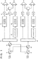
- FIG. 1 is a configuration of an optical receiver according to one embodiment.
- Signal light from an optical transmitter is input to a polarization beam separator 11.
- the polarization beam splitter 11 polarization-separates the signal light, and outputs a Y polarized component Sy of the signal light to a polarization beam splitter 13, and outputs an X polarized component Sx of the signal light to a polarization beam splitter 14.
- the X polarized component Sx and the Y polarized component Sy of the signal light are respectively referred to as signal light Sx and signal light Sy.
- local light generated by an unshown light source is input to a polarization beam splitter 12.
- the polarization beam splitter 12 polarization-separates the local light, and outputs a Y polarized component Ly of the local light to the polarization beam splitter 14, and outputs an X polarized component Lx of the local light to the polarization beam splitter 13.
- the X polarized component Lx and the Y polarized component Ly of the local light are respectively referred to as local light Lx and local light Ly.
- the X polarization plane and the Y polarization plane are orthogonal to each other.
- the polarization beam splitter 13 outputs an optical signal (combined light) including the signal light Sy and the local light Lx to a 1 ⁇ 3 coupler 21, and the optical beam splitter 14 outputs an optical signal (combined light) including the signal light Sx and the local light Ly to a 1 ⁇ 3 coupler 22.
- the 1 ⁇ 3 couplers 21 and 22 each branch the input optical signal to three optical signals having an equal amplitude (equal power), and outputs the three optical signals.
- One of the three optical signals output from the 1 ⁇ 3 coupler 21 is input to a PD 52.
- the PD 52 outputs an electric signal corresponding to the power of the input optical signal to a branching unit 61.
- One of the three optical signals output from the 1 ⁇ 3 coupler 21 is input to a 45 degree polarizer 41.
- the 45 degree polarizer 41 allows only components (hereinafter, referred to as 45 degree components) of polarization plane having an angle of 45 degrees relative to each of the X polarization plane and the Y polarization plane to pass through.
- the optical signal that has passed through the 45 degree polarizer 41 is input to a PD 51. Therefore, the PD 51 outputs a beat signal of the 45 degree component of the signal light Sy and the 45 degree component of the local light Lx as an electric signal.
- One of the three optical signals output from the 1 ⁇ 3 coupler 21 is, after passing through a 1/4 wave plate 31, input to a 45 degree polarizer 42.
- the 1/4 wave plate 31 delays Y polarized light by 1/4 wavelength relative to X polarized light, and outputs the resultant light to a 45 degree polarizer 42.
- the 1/4 wave plate 31 may delay X polarized light by 1/4 wavelength relative to Y polarized light.
- the 45 degree polarizer 42 allows only components (45 degree components) having an angle of 45 degrees relative to each of the X polarization plane and the Y polarization plane to pass through.
- the optical signal that has passed through the 45 degree polarizer 42 is input to a PD 53.
- the PD 53 outputs a beat signal of the 45 degree component of the signal light Sy and the 45 degree component of the local light Lx as an electric signal. Note that the 45 degree component of the signal light Sy input to the PD 53 is delayed by 1/4 wavelength by the 1/4 wave plate 31.
- the electric signal output from the PD 51 is input to a plus terminal of the subtracter 71, and the electric signal output from the PD 53 is input to a plus terminal of the subtracter 72.
- the electric signal output from the PD 52 is branched by a branching unit 61, and the branched electric signals are respectively input to minus terminals of the subtracters 71 and 72. Note that the amplitude of each of the two electric signals output from the branching unit 61 is assumed to be half the amplitude of the electric signal output from the PD 52.
- the subtracters 71 and 72 each output an electric signal obtained by subtracting the electric signal input to the minus terminal from the electric signal input to the plus terminal.
- the electric signals output from the subtracters 71 and 72 are converted to digital signals by unshown ADCs, and the digital signals are input to a processing circuit such as a DSP.
- the reason why demodulation is possible with the configuration in FIG. 1 will be described.
- the Stokes parameters with respect to a combined light including the signal light Sy and the local light Lx that is output from the 1 ⁇ 3 coupler 21 will be described.
- the local light Lx is expressed by a complex number Ex
- the signal light Sy is expressed by a complex number Ey
- the Stokes parameters S 0 , S 1 , S 2 , and S 3 of the combined light are respectively expressed by the following equations.
- Equations (3) and (4) Ex* in Equations (3) and (4) is a complex conjugate of Ex, and Re and Im respectively mean extracting a real part and an imaginary part.
- S 2 +jS 3 corresponds to a signal obtained by performing coherent detection on the signal light Sy, and the signal light Sy can be demodulated by calculating S 2 +jS 3 .
- An optical signal which is the measurement target, is branched into four signals having an equal amplitude (equal power), and the branched signals are respectively input to circuits 81 to 84 shown in FIG. 2 .
- a PD outputs a current I 0 corresponding to the total light receiving amount of a branched light.
- the circuit 82 in FIG. 2 only the light component of a reference polarization plane of the branch light is extracted using a 0 degree polarizer, and a PD outputs a current I 1 corresponding to this light component.
- the light component of a polarization plane having an angle of 45 degrees relative to the reference polarization plane is extracted from the branched light, and a PD outputs a current I 2 corresponding to this light component.
- the phase of a light component of a polarization plane having an angle of 90 degrees relative to the reference polarization plane is delayed by 1/4 wavelength, and thereafter, a light component of a polarization plane having an angle of 45 degrees relative to the reference polarization plane is extracted from the branched light, and a PD outputs a current I 3 corresponding to this light component.
- the Stokes parameters can be obtained from the currents I 0 , I 1 , I 2 , and I 3 using the following equations.
- S 0 I 0
- S 1 2 ⁇ I 1 ⁇ I 0
- S 2 2 ⁇ I 2 ⁇ I 0
- S 3 2 ⁇ I 3 ⁇ I 0
- the PD 52 in FIG. 1 corresponds to the circuit 81 in FIG. 2
- the 45 degree polarizer 41 and the PD 51 in FIG. 1 correspond to the circuit 83 in FIG. 2
- the 1/4 wave plate 31, the 45 degree polarizer 42, and the PD 53 in FIG. 1 correspond to the circuit 84 in FIG. 2 . That is, the PD 52 in FIG. 1 outputs the aforementioned current I 0 with respect to the combined light, the PD 51 outputs the aforementioned current I 2 with respect to the combined light, and the PD 53 outputs the aforementioned current I 3 with respect to the combined light.
- S 2 and S 3 can be obtained from Equations (8) and (9) based on the current I 0 output from the PD 52, the current I 2 output from the PD 51, and the current I 3 output from the PD 53.
- the subtracter 71 subtracts half the amplitude of the electric signal (current I 0 ) output from the PD 52 from the electric signal (current I 2 ) output from the PD 51, and therefore the output of the subtracter 71 indicates S 2 .
- the subtracter 72 subtracts half the amplitude of the electric signal (current I 0 ) output from the PD 52 from the electric signal (current I 3 ) output from the PD 53, and therefore the output of the subtracter 72 indicates S 3 .
- the electric signals output from the subtracters 71 and 72 based on the optical signals output from the 1 ⁇ 3 coupler 21 are converted to digital signals, and the digital signals are input to an unshown processing unit. These electric signals correspond to the signals obtained by coherent-detecting the Y polarized component of the signal light, as described above.
- the electric signals output from the two subtracters based on the optical signals output from the 1 ⁇ 3 coupler 22 are converted to digital signals, and the digital signals are input to the unshown processing unit. Because the X polarized component of the original signal light is input to the 1 ⁇ 3 coupler 22, these electric signals correspond to signals obtained by coherent-detecting the X polarized component of the signal light. Therefore, the processing unit can demodulate the signal light based on these four electric signals.
- the configuration can be changed such that the addition/subtraction in an analog domain is performed in a digital domain.
- the three electric signals output from the PDs 51 to 53 are respectively converted to digital signals by three ADCs, and the digital signals are input to the processing unit.
- the value indicated by the digital signal based on the output of the PD 52 is denoted as a first digital value
- the value indicated by the digital signal based on the output of the PD 51 is denoted as a second digital value
- the value indicated by the digital signal based on the output of the PD 53 is denoted as a third digital value.
- the processing unit obtains a fourth digital value by multiplying the first digital value by a predetermined coefficient.
- the processing unit obtains S 2 by subtracting the fourth digital value from the second digital value, and obtains S 3 by subtracting the fourth digital value from the third digital value.
- the processing load in digital computation in the processing unit can be reduced relative to the other configuration of Non-Patent Literature 1.
- the polarization beam splitters 13 and 14 and the 1 ⁇ 3 couplers 21 and 22 in FIG. 1 can also be replaced by 3 ⁇ 3 couplers 23 and 24, as shown in FIG. 3 .
- the 3 ⁇ 3 coupler 23 combines the input signal light Sy and local light Lx, branches the combined light into three light beams, and outputs the three branched light beams.
- the 3 ⁇ 3 coupler 24 combines the input signal light Sx and local light Ly, branches the combined light into three light beams, and outputs the three branched light beams.
- the polarization beam splitter 11 polarization-separates the signal light
- the polarization beam splitter 12 polarization-separates the local light
- the polarization beam splitters 13 and 14 each combine signal light and local light that are orthogonally polarized to each other.
- the polarization beam splitters 11 to 14 can also be replaced by a polarization beam splitter 15, as shown in FIG. 4 .
- the polarization beam splitter 15 shown in FIG. 4 deflects the X polarized component of input light by 90 degrees, and allows the Y polarized component to pass straight.
- the polarization beam splitter 15 outputs light obtained by combining the signal light Sx and the local light Ly, and light obtained by combining the signal light Sy and the local light Lx.
- an MZI (Mach-Zehnder interferometer) type polarization beam splitter can be used as the polarization beam splitter 15 in FIG. 4 , and in this case, the incident directions of the local light and the signal light need not be adjusted so as to be orthogonal to each other.
- the 1 ⁇ 3 couplers 21 and 22 each branch an input optical signal to three optical signals having an equal amplitude (equal power), and output the branched optical signals, and the branching unit 61 outputs electric signals having half the amplitude of the electric signal output from the PD 52.
- the subtracter 71 can output an electric signal indicating S 2 by performing subtraction of the two input signals
- subtracter 72 can output an electric signal indicating S 3 by performing subtraction of the two input signals.
- the electric power of the electric signal output from the branching unit 61 decreases to a quarter of the electric power of the input electric signal.
- branching unit 61 that outputs an electric signal having half the electric power of the electric signal output from the PD 52 is used as the branching unit 61, in order to suppress degradation of the signal-to-noise ratio (SN ratio).
- the branching unit 61 outputs electric signals having an amplitude that is 1/( ⁇ 2) times the amplitude of the electric signal output from the PD 52.
- the amplitude of each of the electric signals input to the plus terminals of the subtracters 71 and 72 must be twice the amplitude of the signal output from the branching unit 61. That is, the amplitude of each of the electric signals input to the plus terminals of the subtracters 71 and 72 must be ⁇ 2 times the amplitude of the signal output from the PD 52.
- the photodiode outputs an electric signal having an amplitude that is proportional to input light power. Therefore, in this case, the 1 ⁇ 3 couplers 21 and 22 each need only branch the input optical signal such that the power ratio of the branched optical signals is ⁇ 2:1: ⁇ 2. That is, the 1 ⁇ 3 coupler 21 need only output an optical signal having power that is ⁇ 2 times the power of the optical signal to be output to the PD 52 to each of the 45 degree polarizer 41 and the 1/4 wave plate 31. The same applies to the 1 ⁇ 3 coupler 22. Also, when the three electric signals output from the PDs 51 to 53 are converted to digital signals, in order to be subjected to processing, by three ADCs, the aforementioned predetermined coefficient need only be 1/ ⁇ 2.
Landscapes
- Physics & Mathematics (AREA)
- General Physics & Mathematics (AREA)
- Optics & Photonics (AREA)
- Electromagnetism (AREA)
- Engineering & Computer Science (AREA)
- Computer Networks & Wireless Communication (AREA)
- Signal Processing (AREA)
- Nonlinear Science (AREA)
- Optical Communication System (AREA)
- Optical Modulation, Optical Deflection, Nonlinear Optics, Optical Demodulation, Optical Logic Elements (AREA)
Applications Claiming Priority (2)
| Application Number | Priority Date | Filing Date | Title |
|---|---|---|---|
| JP2017143411 | 2017-07-25 | ||
| PCT/JP2018/026998 WO2019021917A1 (ja) | 2017-07-25 | 2018-07-19 | 光受信機及びコヒーレント光受信方法 |
Publications (3)
| Publication Number | Publication Date |
|---|---|
| EP3661080A1 true EP3661080A1 (de) | 2020-06-03 |
| EP3661080A4 EP3661080A4 (de) | 2020-08-19 |
| EP3661080B1 EP3661080B1 (de) | 2021-09-01 |
Family
ID=65040216
Family Applications (1)
| Application Number | Title | Priority Date | Filing Date |
|---|---|---|---|
| EP18837341.9A Active EP3661080B1 (de) | 2017-07-25 | 2018-07-19 | Optischer empfänger und kohärentes optisches empfangsverfahren |
Country Status (5)
| Country | Link |
|---|---|
| US (1) | US10841014B2 (de) |
| EP (1) | EP3661080B1 (de) |
| JP (1) | JP6983891B2 (de) |
| CN (1) | CN110945803B (de) |
| WO (1) | WO2019021917A1 (de) |
Families Citing this family (5)
| Publication number | Priority date | Publication date | Assignee | Title |
|---|---|---|---|---|
| CN110945803B (zh) | 2017-07-25 | 2022-04-19 | 凯迪迪爱通信技术有限公司 | 光接收机和相干光接收方法 |
| JP2022012983A (ja) * | 2020-07-02 | 2022-01-18 | 国立大学法人 東京大学 | 光信号処理装置及び光信号処理方法 |
| JP7540982B2 (ja) * | 2021-09-03 | 2024-08-27 | Kddi株式会社 | ライダ装置 |
| JP7824243B2 (ja) * | 2023-02-10 | 2026-03-04 | Kddi株式会社 | 光受信装置 |
| CN119628752B (zh) * | 2024-12-13 | 2025-09-26 | 哈尔滨工业大学 | 一种集成化光学分集接收装置 |
Family Cites Families (14)
| Publication number | Priority date | Publication date | Assignee | Title |
|---|---|---|---|---|
| JPH0734080B2 (ja) * | 1988-10-20 | 1995-04-12 | 富士通株式会社 | コヒーレント光通信用ヘテロダイン検波受信装置 |
| US20040208646A1 (en) * | 2002-01-18 | 2004-10-21 | Seemant Choudhary | System and method for multi-level phase modulated communication |
| US20060159452A1 (en) * | 2003-01-31 | 2006-07-20 | Tucker Rodney S | Polarization resolving heterodyne optical receiver |
| US7209670B2 (en) * | 2003-04-29 | 2007-04-24 | Nortel Networks Limited | Polarization diversity receiver for optical transmission system |
| JP4170298B2 (ja) * | 2005-01-31 | 2008-10-22 | 富士通株式会社 | 差分4位相偏移変調方式に対応した光受信器および光受信方法 |
| JP4531740B2 (ja) * | 2006-12-15 | 2010-08-25 | 富士通株式会社 | コヒーレント光受信機 |
| JP5437858B2 (ja) * | 2010-03-05 | 2014-03-12 | 富士通テレコムネットワークス株式会社 | 光伝送システム |
| JP5737874B2 (ja) * | 2010-07-06 | 2015-06-17 | 日本オクラロ株式会社 | 復調器及び光送受信機 |
| EP2541810B1 (de) * | 2011-06-29 | 2014-09-24 | Alcatel Lucent | Verfahren zur Demodulation eines phasenmodulierten optischen Signals |
| US8989571B2 (en) * | 2012-09-14 | 2015-03-24 | Fujitsu Limited | In-band supervisory data modulation using complementary power modulation |
| JP2015136015A (ja) * | 2014-01-16 | 2015-07-27 | 国立大学法人 東京大学 | 光信号受信装置、ストークスベクトル処理回路及び光信号送受信システム |
| US10116410B2 (en) * | 2014-09-19 | 2018-10-30 | Telefonaktiebolaget Lm Ericsson (Publ) | Optical transmitters and receivers using polarization multiplexing |
| JP2017143411A (ja) | 2016-02-10 | 2017-08-17 | パナソニックIpマネジメント株式会社 | タイムインターリーブ型ad変換装置、受信装置、及び通信装置 |
| CN110945803B (zh) | 2017-07-25 | 2022-04-19 | 凯迪迪爱通信技术有限公司 | 光接收机和相干光接收方法 |
-
2018
- 2018-07-19 CN CN201880048057.5A patent/CN110945803B/zh active Active
- 2018-07-19 EP EP18837341.9A patent/EP3661080B1/de active Active
- 2018-07-19 JP JP2019532541A patent/JP6983891B2/ja active Active
- 2018-07-19 WO PCT/JP2018/026998 patent/WO2019021917A1/ja not_active Ceased
-
2019
- 2019-10-24 US US16/662,516 patent/US10841014B2/en active Active
Also Published As
| Publication number | Publication date |
|---|---|
| EP3661080A4 (de) | 2020-08-19 |
| WO2019021917A1 (ja) | 2019-01-31 |
| CN110945803A (zh) | 2020-03-31 |
| US20200059302A1 (en) | 2020-02-20 |
| JPWO2019021917A1 (ja) | 2020-03-19 |
| EP3661080B1 (de) | 2021-09-01 |
| CN110945803B (zh) | 2022-04-19 |
| US10841014B2 (en) | 2020-11-17 |
| JP6983891B2 (ja) | 2021-12-17 |
Similar Documents
| Publication | Publication Date | Title |
|---|---|---|
| US10841014B2 (en) | Optical receiver and coherent optical reception method | |
| JP5340004B2 (ja) | バランス補償型光バランスド受信器及び光iq受信器 | |
| JP5326584B2 (ja) | 遅延処理装置,信号増幅装置,光電変換装置,アナログ/デジタル変換装置,受信装置および受信方法 | |
| US8725006B2 (en) | Digital signal-to-signal beat noise reduction for filter-less coherent receiving system | |
| US8977140B2 (en) | Optical receiver and optical reception method | |
| JP7427094B2 (ja) | コヒーレント光受信装置およびコヒーレント光受信装置を使用した光学システム | |
| US8768180B2 (en) | All-optical, phase sensitive optical signal sampling | |
| US8849130B2 (en) | Coherent optical receivers for colorless reception | |
| US10090933B2 (en) | Polarization insensitive self-homodyne detection receiver | |
| CN112291018B (zh) | 一种相干接收机的光电接收装置、接收方法及相干接收机 | |
| CN105850051B (zh) | 一种接收机 | |
| JP7318886B2 (ja) | 光受信装置 | |
| JP6761782B2 (ja) | 光受信機及びコヒーレント光受信方法 | |
| JP7340190B2 (ja) | 光受信装置 | |
| JP5312366B2 (ja) | 光受信器 | |
| CN118784087A (zh) | 偏振复用信号直接检测方法、装置、设备及存储介质 | |
| JP2012015634A (ja) | 偏波多重差動位相変調光伝送システムにおける受信装置 |
Legal Events
| Date | Code | Title | Description |
|---|---|---|---|
| STAA | Information on the status of an ep patent application or granted ep patent |
Free format text: STATUS: THE INTERNATIONAL PUBLICATION HAS BEEN MADE |
|
| PUAI | Public reference made under article 153(3) epc to a published international application that has entered the european phase |
Free format text: ORIGINAL CODE: 0009012 |
|
| STAA | Information on the status of an ep patent application or granted ep patent |
Free format text: STATUS: REQUEST FOR EXAMINATION WAS MADE |
|
| 17P | Request for examination filed |
Effective date: 20191029 |
|
| AK | Designated contracting states |
Kind code of ref document: A1 Designated state(s): AL AT BE BG CH CY CZ DE DK EE ES FI FR GB GR HR HU IE IS IT LI LT LU LV MC MK MT NL NO PL PT RO RS SE SI SK SM TR |
|
| AX | Request for extension of the european patent |
Extension state: BA ME |
|
| A4 | Supplementary search report drawn up and despatched |
Effective date: 20200716 |
|
| RIC1 | Information provided on ipc code assigned before grant |
Ipc: H04J 14/06 20060101ALI20200710BHEP Ipc: G02F 2/00 20060101ALI20200710BHEP Ipc: H04B 10/61 20130101AFI20200710BHEP |
|
| DAV | Request for validation of the european patent (deleted) | ||
| DAX | Request for extension of the european patent (deleted) | ||
| GRAP | Despatch of communication of intention to grant a patent |
Free format text: ORIGINAL CODE: EPIDOSNIGR1 |
|
| STAA | Information on the status of an ep patent application or granted ep patent |
Free format text: STATUS: GRANT OF PATENT IS INTENDED |
|
| INTG | Intention to grant announced |
Effective date: 20210414 |
|
| GRAS | Grant fee paid |
Free format text: ORIGINAL CODE: EPIDOSNIGR3 |
|
| GRAA | (expected) grant |
Free format text: ORIGINAL CODE: 0009210 |
|
| STAA | Information on the status of an ep patent application or granted ep patent |
Free format text: STATUS: THE PATENT HAS BEEN GRANTED |
|
| AK | Designated contracting states |
Kind code of ref document: B1 Designated state(s): AL AT BE BG CH CY CZ DE DK EE ES FI FR GB GR HR HU IE IS IT LI LT LU LV MC MK MT NL NO PL PT RO RS SE SI SK SM TR |
|
| REG | Reference to a national code |
Ref country code: GB Ref legal event code: FG4D |
|
| REG | Reference to a national code |
Ref country code: CH Ref legal event code: EP Ref country code: AT Ref legal event code: REF Ref document number: 1427329 Country of ref document: AT Kind code of ref document: T Effective date: 20210915 |
|
| REG | Reference to a national code |
Ref country code: DE Ref legal event code: R096 Ref document number: 602018023058 Country of ref document: DE |
|
| REG | Reference to a national code |
Ref country code: IE Ref legal event code: FG4D |
|
| REG | Reference to a national code |
Ref country code: LT Ref legal event code: MG9D |
|
| REG | Reference to a national code |
Ref country code: NL Ref legal event code: MP Effective date: 20210901 |
|
| PG25 | Lapsed in a contracting state [announced via postgrant information from national office to epo] |
Ref country code: NO Free format text: LAPSE BECAUSE OF FAILURE TO SUBMIT A TRANSLATION OF THE DESCRIPTION OR TO PAY THE FEE WITHIN THE PRESCRIBED TIME-LIMIT Effective date: 20211201 Ref country code: HR Free format text: LAPSE BECAUSE OF FAILURE TO SUBMIT A TRANSLATION OF THE DESCRIPTION OR TO PAY THE FEE WITHIN THE PRESCRIBED TIME-LIMIT Effective date: 20210901 Ref country code: LT Free format text: LAPSE BECAUSE OF FAILURE TO SUBMIT A TRANSLATION OF THE DESCRIPTION OR TO PAY THE FEE WITHIN THE PRESCRIBED TIME-LIMIT Effective date: 20210901 Ref country code: BG Free format text: LAPSE BECAUSE OF FAILURE TO SUBMIT A TRANSLATION OF THE DESCRIPTION OR TO PAY THE FEE WITHIN THE PRESCRIBED TIME-LIMIT Effective date: 20211201 Ref country code: FI Free format text: LAPSE BECAUSE OF FAILURE TO SUBMIT A TRANSLATION OF THE DESCRIPTION OR TO PAY THE FEE WITHIN THE PRESCRIBED TIME-LIMIT Effective date: 20210901 Ref country code: ES Free format text: LAPSE BECAUSE OF FAILURE TO SUBMIT A TRANSLATION OF THE DESCRIPTION OR TO PAY THE FEE WITHIN THE PRESCRIBED TIME-LIMIT Effective date: 20210901 Ref country code: SE Free format text: LAPSE BECAUSE OF FAILURE TO SUBMIT A TRANSLATION OF THE DESCRIPTION OR TO PAY THE FEE WITHIN THE PRESCRIBED TIME-LIMIT Effective date: 20210901 Ref country code: RS Free format text: LAPSE BECAUSE OF FAILURE TO SUBMIT A TRANSLATION OF THE DESCRIPTION OR TO PAY THE FEE WITHIN THE PRESCRIBED TIME-LIMIT Effective date: 20210901 |
|
| REG | Reference to a national code |
Ref country code: AT Ref legal event code: MK05 Ref document number: 1427329 Country of ref document: AT Kind code of ref document: T Effective date: 20210901 |
|
| PG25 | Lapsed in a contracting state [announced via postgrant information from national office to epo] |
Ref country code: PL Free format text: LAPSE BECAUSE OF FAILURE TO SUBMIT A TRANSLATION OF THE DESCRIPTION OR TO PAY THE FEE WITHIN THE PRESCRIBED TIME-LIMIT Effective date: 20210901 Ref country code: LV Free format text: LAPSE BECAUSE OF FAILURE TO SUBMIT A TRANSLATION OF THE DESCRIPTION OR TO PAY THE FEE WITHIN THE PRESCRIBED TIME-LIMIT Effective date: 20210901 Ref country code: GR Free format text: LAPSE BECAUSE OF FAILURE TO SUBMIT A TRANSLATION OF THE DESCRIPTION OR TO PAY THE FEE WITHIN THE PRESCRIBED TIME-LIMIT Effective date: 20211202 |
|
| PG25 | Lapsed in a contracting state [announced via postgrant information from national office to epo] |
Ref country code: AT Free format text: LAPSE BECAUSE OF FAILURE TO SUBMIT A TRANSLATION OF THE DESCRIPTION OR TO PAY THE FEE WITHIN THE PRESCRIBED TIME-LIMIT Effective date: 20210901 |
|
| PG25 | Lapsed in a contracting state [announced via postgrant information from national office to epo] |
Ref country code: IS Free format text: LAPSE BECAUSE OF FAILURE TO SUBMIT A TRANSLATION OF THE DESCRIPTION OR TO PAY THE FEE WITHIN THE PRESCRIBED TIME-LIMIT Effective date: 20220101 Ref country code: SM Free format text: LAPSE BECAUSE OF FAILURE TO SUBMIT A TRANSLATION OF THE DESCRIPTION OR TO PAY THE FEE WITHIN THE PRESCRIBED TIME-LIMIT Effective date: 20210901 Ref country code: SK Free format text: LAPSE BECAUSE OF FAILURE TO SUBMIT A TRANSLATION OF THE DESCRIPTION OR TO PAY THE FEE WITHIN THE PRESCRIBED TIME-LIMIT Effective date: 20210901 Ref country code: RO Free format text: LAPSE BECAUSE OF FAILURE TO SUBMIT A TRANSLATION OF THE DESCRIPTION OR TO PAY THE FEE WITHIN THE PRESCRIBED TIME-LIMIT Effective date: 20210901 Ref country code: PT Free format text: LAPSE BECAUSE OF FAILURE TO SUBMIT A TRANSLATION OF THE DESCRIPTION OR TO PAY THE FEE WITHIN THE PRESCRIBED TIME-LIMIT Effective date: 20220103 Ref country code: NL Free format text: LAPSE BECAUSE OF FAILURE TO SUBMIT A TRANSLATION OF THE DESCRIPTION OR TO PAY THE FEE WITHIN THE PRESCRIBED TIME-LIMIT Effective date: 20210901 Ref country code: EE Free format text: LAPSE BECAUSE OF FAILURE TO SUBMIT A TRANSLATION OF THE DESCRIPTION OR TO PAY THE FEE WITHIN THE PRESCRIBED TIME-LIMIT Effective date: 20210901 Ref country code: CZ Free format text: LAPSE BECAUSE OF FAILURE TO SUBMIT A TRANSLATION OF THE DESCRIPTION OR TO PAY THE FEE WITHIN THE PRESCRIBED TIME-LIMIT Effective date: 20210901 Ref country code: AL Free format text: LAPSE BECAUSE OF FAILURE TO SUBMIT A TRANSLATION OF THE DESCRIPTION OR TO PAY THE FEE WITHIN THE PRESCRIBED TIME-LIMIT Effective date: 20210901 |
|
| REG | Reference to a national code |
Ref country code: DE Ref legal event code: R097 Ref document number: 602018023058 Country of ref document: DE |
|
| PLBE | No opposition filed within time limit |
Free format text: ORIGINAL CODE: 0009261 |
|
| STAA | Information on the status of an ep patent application or granted ep patent |
Free format text: STATUS: NO OPPOSITION FILED WITHIN TIME LIMIT |
|
| PG25 | Lapsed in a contracting state [announced via postgrant information from national office to epo] |
Ref country code: IT Free format text: LAPSE BECAUSE OF FAILURE TO SUBMIT A TRANSLATION OF THE DESCRIPTION OR TO PAY THE FEE WITHIN THE PRESCRIBED TIME-LIMIT Effective date: 20210901 Ref country code: DK Free format text: LAPSE BECAUSE OF FAILURE TO SUBMIT A TRANSLATION OF THE DESCRIPTION OR TO PAY THE FEE WITHIN THE PRESCRIBED TIME-LIMIT Effective date: 20210901 |
|
| 26N | No opposition filed |
Effective date: 20220602 |
|
| PG25 | Lapsed in a contracting state [announced via postgrant information from national office to epo] |
Ref country code: SI Free format text: LAPSE BECAUSE OF FAILURE TO SUBMIT A TRANSLATION OF THE DESCRIPTION OR TO PAY THE FEE WITHIN THE PRESCRIBED TIME-LIMIT Effective date: 20210901 |
|
| PG25 | Lapsed in a contracting state [announced via postgrant information from national office to epo] |
Ref country code: MC Free format text: LAPSE BECAUSE OF FAILURE TO SUBMIT A TRANSLATION OF THE DESCRIPTION OR TO PAY THE FEE WITHIN THE PRESCRIBED TIME-LIMIT Effective date: 20210901 |
|
| REG | Reference to a national code |
Ref country code: CH Ref legal event code: PL |
|
| REG | Reference to a national code |
Ref country code: BE Ref legal event code: MM Effective date: 20220731 |
|
| PG25 | Lapsed in a contracting state [announced via postgrant information from national office to epo] |
Ref country code: LU Free format text: LAPSE BECAUSE OF NON-PAYMENT OF DUE FEES Effective date: 20220719 Ref country code: LI Free format text: LAPSE BECAUSE OF NON-PAYMENT OF DUE FEES Effective date: 20220731 Ref country code: CH Free format text: LAPSE BECAUSE OF NON-PAYMENT OF DUE FEES Effective date: 20220731 |
|
| PG25 | Lapsed in a contracting state [announced via postgrant information from national office to epo] |
Ref country code: BE Free format text: LAPSE BECAUSE OF NON-PAYMENT OF DUE FEES Effective date: 20220731 |
|
| PG25 | Lapsed in a contracting state [announced via postgrant information from national office to epo] |
Ref country code: IE Free format text: LAPSE BECAUSE OF NON-PAYMENT OF DUE FEES Effective date: 20220719 |
|
| PG25 | Lapsed in a contracting state [announced via postgrant information from national office to epo] |
Ref country code: MK Free format text: LAPSE BECAUSE OF FAILURE TO SUBMIT A TRANSLATION OF THE DESCRIPTION OR TO PAY THE FEE WITHIN THE PRESCRIBED TIME-LIMIT Effective date: 20210901 Ref country code: CY Free format text: LAPSE BECAUSE OF FAILURE TO SUBMIT A TRANSLATION OF THE DESCRIPTION OR TO PAY THE FEE WITHIN THE PRESCRIBED TIME-LIMIT Effective date: 20210901 |
|
| PG25 | Lapsed in a contracting state [announced via postgrant information from national office to epo] |
Ref country code: HU Free format text: LAPSE BECAUSE OF FAILURE TO SUBMIT A TRANSLATION OF THE DESCRIPTION OR TO PAY THE FEE WITHIN THE PRESCRIBED TIME-LIMIT; INVALID AB INITIO Effective date: 20180719 |
|
| PG25 | Lapsed in a contracting state [announced via postgrant information from national office to epo] |
Ref country code: MT Free format text: LAPSE BECAUSE OF FAILURE TO SUBMIT A TRANSLATION OF THE DESCRIPTION OR TO PAY THE FEE WITHIN THE PRESCRIBED TIME-LIMIT Effective date: 20210901 |
|
| PGFP | Annual fee paid to national office [announced via postgrant information from national office to epo] |
Ref country code: DE Payment date: 20250722 Year of fee payment: 8 |
|
| PGFP | Annual fee paid to national office [announced via postgrant information from national office to epo] |
Ref country code: GB Payment date: 20250722 Year of fee payment: 8 |
|
| PGFP | Annual fee paid to national office [announced via postgrant information from national office to epo] |
Ref country code: FR Payment date: 20250725 Year of fee payment: 8 |
|
| PG25 | Lapsed in a contracting state [announced via postgrant information from national office to epo] |
Ref country code: TR Free format text: LAPSE BECAUSE OF FAILURE TO SUBMIT A TRANSLATION OF THE DESCRIPTION OR TO PAY THE FEE WITHIN THE PRESCRIBED TIME-LIMIT Effective date: 20210901 |