EP3639166B1 - Retikel optimierungsalgorithmen und optimales zieldesign - Google Patents
Retikel optimierungsalgorithmen und optimales zieldesign Download PDFInfo
- Publication number
- EP3639166B1 EP3639166B1 EP17912654.5A EP17912654A EP3639166B1 EP 3639166 B1 EP3639166 B1 EP 3639166B1 EP 17912654 A EP17912654 A EP 17912654A EP 3639166 B1 EP3639166 B1 EP 3639166B1
- Authority
- EP
- European Patent Office
- Prior art keywords
- target
- sub
- metrology
- pitch
- measurement direction
- Prior art date
- Legal status (The legal status is an assumption and is not a legal conclusion. Google has not performed a legal analysis and makes no representation as to the accuracy of the status listed.)
- Active
Links
Images




Classifications
-
- G—PHYSICS
- G03—PHOTOGRAPHY; CINEMATOGRAPHY; ANALOGOUS TECHNIQUES USING WAVES OTHER THAN OPTICAL WAVES; ELECTROGRAPHY; HOLOGRAPHY
- G03F—PHOTOMECHANICAL PRODUCTION OF TEXTURED OR PATTERNED SURFACES, e.g. FOR PRINTING, FOR PROCESSING OF SEMICONDUCTOR DEVICES; MATERIALS THEREFOR; ORIGINALS THEREFOR; APPARATUS SPECIALLY ADAPTED THEREFOR
- G03F7/00—Photomechanical, e.g. photolithographic, production of textured or patterned surfaces, e.g. printing surfaces; Materials therefor, e.g. comprising photoresists; Apparatus specially adapted therefor
- G03F7/70—Microphotolithographic exposure; Apparatus therefor
- G03F7/70483—Information management; Active and passive control; Testing; Wafer monitoring, e.g. pattern monitoring
- G03F7/70605—Workpiece metrology
- G03F7/70616—Monitoring the printed patterns
- G03F7/70633—Overlay, i.e. relative alignment between patterns printed by separate exposures in different layers, or in the same layer in multiple exposures or stitching
-
- G—PHYSICS
- G03—PHOTOGRAPHY; CINEMATOGRAPHY; ANALOGOUS TECHNIQUES USING WAVES OTHER THAN OPTICAL WAVES; ELECTROGRAPHY; HOLOGRAPHY
- G03F—PHOTOMECHANICAL PRODUCTION OF TEXTURED OR PATTERNED SURFACES, e.g. FOR PRINTING, FOR PROCESSING OF SEMICONDUCTOR DEVICES; MATERIALS THEREFOR; ORIGINALS THEREFOR; APPARATUS SPECIALLY ADAPTED THEREFOR
- G03F1/00—Originals for photomechanical production of textured or patterned surfaces, e.g., masks, photo-masks, reticles; Mask blanks or pellicles therefor; Containers specially adapted therefor; Preparation thereof
- G03F1/38—Masks having auxiliary features, e.g. special coatings or marks for alignment or testing; Preparation thereof
- G03F1/44—Testing or measuring features, e.g. grid patterns, focus monitors, sawtooth scales or notched scales
-
- G—PHYSICS
- G03—PHOTOGRAPHY; CINEMATOGRAPHY; ANALOGOUS TECHNIQUES USING WAVES OTHER THAN OPTICAL WAVES; ELECTROGRAPHY; HOLOGRAPHY
- G03F—PHOTOMECHANICAL PRODUCTION OF TEXTURED OR PATTERNED SURFACES, e.g. FOR PRINTING, FOR PROCESSING OF SEMICONDUCTOR DEVICES; MATERIALS THEREFOR; ORIGINALS THEREFOR; APPARATUS SPECIALLY ADAPTED THEREFOR
- G03F7/00—Photomechanical, e.g. photolithographic, production of textured or patterned surfaces, e.g. printing surfaces; Materials therefor, e.g. comprising photoresists; Apparatus specially adapted therefor
- G03F7/70—Microphotolithographic exposure; Apparatus therefor
- G03F7/70058—Mask illumination systems
- G03F7/7015—Details of optical elements
-
- G—PHYSICS
- G03—PHOTOGRAPHY; CINEMATOGRAPHY; ANALOGOUS TECHNIQUES USING WAVES OTHER THAN OPTICAL WAVES; ELECTROGRAPHY; HOLOGRAPHY
- G03F—PHOTOMECHANICAL PRODUCTION OF TEXTURED OR PATTERNED SURFACES, e.g. FOR PRINTING, FOR PROCESSING OF SEMICONDUCTOR DEVICES; MATERIALS THEREFOR; ORIGINALS THEREFOR; APPARATUS SPECIALLY ADAPTED THEREFOR
- G03F7/00—Photomechanical, e.g. photolithographic, production of textured or patterned surfaces, e.g. printing surfaces; Materials therefor, e.g. comprising photoresists; Apparatus specially adapted therefor
- G03F7/70—Microphotolithographic exposure; Apparatus therefor
- G03F7/70483—Information management; Active and passive control; Testing; Wafer monitoring, e.g. pattern monitoring
- G03F7/70605—Workpiece metrology
- G03F7/70681—Metrology strategies
- G03F7/70683—Mark designs
Definitions
- the present invention relates to the field of metrology, and more particularly, to overlay target design.
- US2017/146810 discloses metrology targets and methods which provide self-Moiré measurements of unresolved target features.
- WO2016/123552 describes device metrology targets and methods.
- WO2015/153497 discloses target designs and methods which relate to periodic structures having elements recurring with a first pitch in a first direction.
- US2017/146915 discloses topographic phase control for overlay measurement.
- US2016/062231 describes a method for fabricating a photolithographic mask.
- One aspect of the present invention provides a metrology target design as recited in claim 1.
- a second aspect of the present invention as recited in claim 8 provides a method of producing a configurable metrology target on a wafer using the metrology target design.
- Overlay control is one of the main challenges of current lithography. Generally it is achieved by printing special marks, or targets on the wafer, with respect to which the overlay is measured. During the design of the mask, or reticle, the printability (process window) and aberration stability issues must be taken into account. This makes the design of the mask a very difficult task, which includes both simulations and experimental parts.
- One of the ways to handle the problem is the usage of the assist unprintable features on the mask (Assist Sub-Resolution Features ASRAF). These features are not printed by themselves (as they are sub-resolved), however they improve printability of the designed structures and reduce their sensitivity to scanner's aberrations. However, the usage of assist features adds a huge number of degrees of freedom which together with the absence of generic methodology pushes the target design domain to use a trial and error approach.
- disclosed target designs and methods make the design process of overlay targets more intuitive and predictable, by combining CD-modulation and field-modulation targets with an orthogonal periodic structure, perpendicular to the measurement direction and having an unresolved pitch.
- Target designs on the reticle and on the wafer, and target design and processing methods comprise coarse pitched periodic structures having fine pitched sub-elements, which vary in sub-element CD and/or height, an orthogonal periodic structure, perpendicular to the measurement direction, with an orthogonal unresolved pitch among periodically recurring bars, which provide a calibration parameter for achieving well-printed targets.
- Orthogonal periodic structures may be designed on the reticle and be unresolved, or be applied in cut patterns on the process layer, with relatively low sensitivity to the cut layer overlay. Designed targets may be used for overlay metrology as well as for measuring process parameters such as scanner aberrations and pitch walk.
- FIG. 1A is a high level schematic illustration of a metrology target design 100, according to some embodiments of the invention. Illustrated is target design 100 on the reticle (photoreticle, used in lithography to define patterned layers on the wafer, also termed mask or photomask), which is used to produce a corresponding target on the wafer, which may have some different features, as explained below.
- Metrology target design 100 comprises a periodic structure along a measurement direction, having a coarse pitch P among periodically recurring elements 110. Each element 110 is periodic along the measurement direction with a fine pitch P1 among periodically recurring sub-elements 120.
- Target design 100 further comprises an orthogonal periodic structure having periodically recurring bars 130, perpendicular to the measurement direction, with an orthogonal unresolved pitch P2 among periodically recurring bars 130, which have a CD of CD(B).
- the unresolved orthogonal pitch P2 is smaller than a specified minimal design rule pitch and is therefore not printed on the wafer itself, but merely help provides controllable targets, as explained below.
- element 110 is denoted somewhat arbitrarily as a unit cell, and could have been chosen in different locations of metrology target design 100.
- FIG. 1B is a high level schematic and highly simplified illustration of the settings of the lithography process, according to some embodiments of the invention.
- Targets 150 on a wafer 104 are produced using illumination from illumination source 70 which is projected through a reticle 102 (also termed mask) with target design 100 thereupon.
- reticle 102 typically includes circuit design data and possibly multiple target designs 100, relating to one, or possibly more layers of integrated circuit(s) produced on wafer 104.
- the disclosed description of target designs 100 and targets 150 relates merely to these components on reticle 102 and wafer 104, respectively, and are typically part of much more complex designs.
- Certain embodiments comprise lithography reticle(s) 102 comprising metrology target designs 100 disclosed herein.
- Certain embodiments comprise wafers 104 comprising metrology target(s) 150 produced using metrology target design(s) 100 disclosed herein, as well as metrology target(s) 150 themselves. Certain embodiments comprise target design file of metrology target(s) 150. Certain embodiments comprise metrology overlay measurements target design file of metrology targets 150.
- target coarse pitch P(T) is an integer multiple of target fine pitch P1(T)
- P(T) n ⁇ P1(T) for integer n.
- Non-limiting examples for metrology target(s) 150 are presented in Figure 5 .
- FIGs 2A-2C are high level schematic illustrations of prior art target designs 80.
- typical target design for overlay measurements comprises a periodic structure with elements 82 set at a pitch P.
- Target design on the reticle and actual target geometry are similar as all elements 82 are printed.
- pitch P is large (much larger than the minimal design rule, typically larger than 1000nm, as required for achieving optical resolution with the illumination spectrum in the visual range.
- designs 80 leaves wide empty spaces and wide unsegmented bar 82 they are generally process incompatible and cause significant bias with respect to devices due to asymmetric scanner aberrations.
- FIGS 2B and 2C illustrate, respectively, prior art target designs 90, 95 on the reticle and on the wafer, respectively.
- Prior art design 90 includes segmentation of wide bars 82 into a finely segmented periodic structure, having elements 92 repeating with a fine pitch P1, which yields device-like structures within the coarse pitch P.
- elements 92 have pitch P1 which is in the order of magnitude or even the same as device structures (minimal design rule pitch), and the required optical resolution is achieved by setting the parameters of device-like printed structures 97 to vary over the coarse pitch, as disclosed in more details in U.S. Patent Application No. 14/820917 and WIPO Application No. PCT/US16/60626 .
- targets designs 90 have too many free parameters which influence the resulting performance, and optimizing all of them simultaneously may be a quite difficult task.
- the free parameters include the width values of each of bars 92 and make sure that all bars 92 are printed and have a large enough process window. This is a significant challenge, requiring well-calibrated simulations which are rarely available due to the difficulty of calibrating the chemistry of the resist, which is therefore typically handled by a trial and error approach.
- this prior art approach almost inapplicable.
- the inventors have found out that analysis is hampered by discontinuities and non-differentiable regions, which also prevent forming intuitive rules of thumb for guessing the conditions for target 95 to be well-printed.
- the inventors suggest, in target designs 100, to reduce significantly the number of varying parameters in target design 100 and to use parameters which affect the target printability in an intuitive way from a physical point of view. Since the main printability problem is connected to the luck of knowning of correct value of aerial image threshold, the inventors suggested using orthogonal bars 130 to control the printability of sub-elements 120 and their parameters, while keeping orthogonal bars 130 themselves not printed and unresolved in direction perpendicular to printed structures 155.
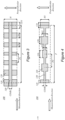
- Figures 3 and 4 are high level schematic illustrations of metrology target design 100, according to some embodiments of the invention. It is noted that Figures 3 and 4 merely illustrate a small part of respective target designs 100, for the purpose of explaining their design principles, namely that (i) added orthogonal pattern 130 is periodic in the perpendicular direction (to the measurement direction) and has pitch P2 (see Figure 1A ) which is smaller than the minimal design rule pitch and is therefore unresolved by the printing tool's optical system; (ii) added orthogonal pattern 130 does not affect the positions of the diffraction orders (from elements 110, 120 in the measurement direction) in the pupil plane of the metrology system and, correspondingly, in quasi two-beam imaging scheme provided by CD modulation targets (having different CD's for sub-elements 120), pattern 130 does not change the position of the printed pattern in the field plane (causing no bias with respect to the devices); and (iii) by varying the width (CD(B)) of orthogonal bars 130, the intensity of zero and first
- Figure 5 is a high level schematic illustration of printed metrology targets 150 using target designs 100 with varying width (CD(B)) of orthogonal bars 130, according to some embodiments of the invention.
- Printed metrology targets 150 illustrated in Figure 5 were printed using target designs 100 illustrated in Figure 1A and 3 , as non-limiting examples.
- Figure 5 demonstrates that varying the width (CD(B)) of orthogonal bars 130 results in different widths (CD's) of target sub-elements 155, allowing simple selection of the optimal CD(B).
- orthogonal periodic structure 130 perpendicular to the measurement direction and having an unresolved pitch
- sub-elements 120 may be designed to have varying heights (H1, H2, H3 etc.) instead of (or possibly in addition to) having varying widths (CD1, CD2, CD3, etc.) to provide other (or additional) parameters for the optimization process.
- the modulation in vertical direction may be set to be unresolved and not affect the positions of diffraction orders in the pupil plane, forming no bias with respect to the devices, but still affects the mask's transmittance properties, as explained e.g., in U.S. Patent Application Publication No. 2015/0309402 .
- Target designs 100 such as disclosed in Figure 4 may be used to add additional flexibility (e.g., widths of bars 130 and heights of sub-elements 120) for achieving good printability conditions.
- disclosed embodiments enable using a single parametric relaxation of the optimization process and possibly build the CD-modulation of sub-elements 120 and printed targets 150 with unified parametric sets. Moreover, disclosed embodiments provide innovative mask design capabilities including effective Aerial image threshold control using a single parametric family optimization, and a unified target design optimization relaxation using heights and/or widths of sub-elements 120.
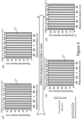
- FIGS 6A-6C are high level schematic illustrations of printed metrology targets 150, according to some embodiments of the invention. It is noted that Figures 6A-6C merely illustrate a small part, corresponding to one period, of respective metrology target production stages 150A, 150B and 150, respectively, for the purpose of explaining their design principles Figures 6A-6C illustrate schematically process stages 150A, 150B for producing targets 150, respectively, on the wafer.
- Metrology targets 150 may comprise periodic structure 151 along the measurement direction, having coarse pitch (P) among periodically recurring elements 151, wherein each element 151 is periodic along the measurement direction with fine pitch (P1) among periodically recurring sub-elements 155 and all sub-elements 155 have the same CD.
- Sub-elements 155 may be cut (moving from patterns 150A to pattern 150B in Figures 6A and 6B , respectively) by an orthogonal periodic structure 160, perpendicular to the measurement direction, having periodically recurring cuts.
- the inventors have found out that the cuts may be configured to simulate CD modulation of printed target 150, and simplify the production process.
- Sub-elements 155 may be configured to represent device structures without any CD variation (thereby avoiding printability problems) while the cutting process transfers these structures into effectively CD-modulated target 150 which is measurable by the metrology optical tool.
- Sub-elements 155 may have varying CD's (as illustrated e.g., in Figures 1A and 1B ) or have a same CD. Disclosed targets 150 with sub-elements 155 with a same CD may have better printability than sub-elements 155 varying CD's and achieve an almost zero offset with respect to device structures. Respective overlay targets 150 may be used for metrology overlay measurements.
- a standard device printing procedure which includes printing of periodic gratings with minimal design rule and subsequent lines cutting in the perpendicular direction, is utilized for producing targets 150. It is noted that as this procedure is applicable only for targets 150 in the process layer as they involve cuts, however just these targets pose a main challenge from the process compatibility point of view.
- Coarse pitch (P) may be configured to be resolved by the metrology tool optics, operating e.g., above 400nm.
- Fine pitch (P1) may be configured to satisfy printing requirements, and cuts 160 may be configured to maintain process compatibility as well, e.g., by leaving no gaps larger than a printability threshold, e.g., 100nm.
- targets 150 do not suffer from printability issues, they also do not impose tough specs on the location of cutting patterns 160, in neither measurement direction or in the perpendicular direction, resulting in a large allowable range of overlay errors for cutting patterns 160, of several nm, possibly even up to 10nm.
- FIGS 7A and 7B are high level schematic illustrations of additional measurements 170 using targets 150, according to some embodiments of the invention. Certain embodiments may utilize targets 150 for additional measurements, such as scanner aberrations measurement 174, pitch walk measurement 176 etc.
- targets 150 for additional measurements such as scanner aberrations measurement 174, pitch walk measurement 176 etc.
- simultaneous targets 150 with segmentation pitches fine pitch P1 in the range from minimal design rule (DR) up to twice the minimal design rule (2 ⁇ DR) may be printed, cut as disclosed above and measured by overlay metrology tools 172.
- the results of overlay measurements between different cells 150 corresponding to different segmentation pitches (fine pitch P1) provide a basis for scanner aberration amplitudes calculation as it is described in U.S. Patent Application No. 14/820917 .
- simultaneous targets 150 may comprise two cells 150A, each representing a periodic structure printed on different steps of the double patterning procedure (multiple cells 150A may be used for measuring pitch walk in a multiple patterning procedure), while other periodic structures in target 150 are transformed into CD modulation targets using the cutting procedure.
- Figure 8 is a high level flowchart illustrating a method 200, according to some embodiments of the invention.
- the method stages may be carried out with respect to target designs 100 and/or targets 150 described above, which may optionally be configured to implement method 200.
- Method 200 may be at least partially implemented by at least one computer processor, e.g., in a metrology module.
- Certain embodiments comprise computer program products comprising a computer readable storage medium having computer readable program embodied therewith and configured to carry out the relevant stages of method 200.
- Certain embodiments comprise target design files of respective targets designed by embodiments of method 200.
- Method 200 may comprise the following stages, irrespective of their order.
- Method 200 may comprise introducing (stage 210), to a metrology target design comprising a periodic structure along a measurement direction, an orthogonal periodic structure having an orthogonal unresolved pitch, perpendicular to the measurement direction, and using (stage 220) the metrology target design on a lithography reticle to produce a configurable metrology target with a periodic structure along the measurement direction only.
- Method 200 may comprise configuring (stage 230) the metrology target design to have the periodic structure comprise periodically recurring elements at a coarse pitch with each element being periodic along the measurement direction with a fine pitch among periodically recurring sub-elements, which vary in sub-element CD, wherein the coarse pitch is an integer multiple of the fine pitch.
- Method 200 may further comprise configuring a width of orthogonal periodic structure elements to optimize target printability (stage 240). Method 200 may further comprise deriving overlay metrology measurements from metrology targets produced from the metrology target design (stage 250).
- Method 200 may comprise producing (stage 260) a periodic structure along a measurement direction on a process layer, the periodic structure having a coarse pitch among periodically recurring elements, wherein each element is periodic along the measurement direction with a fine pitch among periodically recurring sub-elements, which have a same CD; and cutting (stage 270) the sub-elements by an orthogonal periodic structure, perpendicular to the measurement direction, having periodically recurring cuts.
- method 200 may comprise producing the fine pitched sub-elements to have a same CD, and using the cutting to effectively simulate variable CD (stage 272).
- the fine pitch may be configured to be between once and twice a minimal design rule pitch (DR), possibly, twice the DR to broaden the process window (stage 275).
- DR minimal design rule pitch
- Method 200 may further comprise measuring scanner aberrations (stage 280) using a plurality of produced metrology targets having fine pitches between one and two times a minimal design rule, measured by an overlay measurement tool.
- Method 200 may further comprise comprising measuring pitch walk (stage 290) by including in produced metrology targets, periodic cells relating to different steps of a multiple patterning procedure.
- These computer program instructions may also be stored in a computer readable medium that can direct a computer, other programmable data processing apparatus, or other devices to function in a particular manner, such that the instructions stored in the computer readable medium produce an article of manufacture including instructions which implement the function/act specified in the flowchart and/or portion diagram or portions thereof.
- the computer program instructions may also be loaded onto a computer, other programmable data processing apparatus, or other devices to cause a series of operational steps to be performed on the computer, other programmable apparatus or other devices to produce a computer implemented process such that the instructions which execute on the computer or other programmable apparatus provide processes for implementing the functions/acts specified in the flowchart and/or portion diagram or portions thereof.
- each portion in the flowchart or portion diagrams may represent a module, segment, or portion of code, which comprises one or more executable instructions for implementing the specified logical function(s).
- the functions noted in the portion may occur out of the order noted in the figures. For example, two portions shown in succession may, in fact, be executed substantially concurrently, or the portions may sometimes be executed in the reverse order, depending upon the functionality involved.
- each portion of the portion diagrams and/or flowchart illustration, and combinations of portions in the portion diagrams and/or flowchart illustration can be implemented by special purpose hardware-based systems that perform the specified functions or acts, or combinations of special purpose hardware and computer instructions.
Landscapes
- Physics & Mathematics (AREA)
- General Physics & Mathematics (AREA)
- Exposure And Positioning Against Photoresist Photosensitive Materials (AREA)
- Engineering & Computer Science (AREA)
- Computer Hardware Design (AREA)
- Theoretical Computer Science (AREA)
- Preparing Plates And Mask In Photomechanical Process (AREA)
- Evolutionary Computation (AREA)
- Geometry (AREA)
- General Engineering & Computer Science (AREA)
- Exposure Of Semiconductors, Excluding Electron Or Ion Beam Exposure (AREA)
- Electron Beam Exposure (AREA)
Claims (9)
- Messtechnikzieldesign (100), umfassend eine periodische Struktur entlang einer Messrichtung, die eine Grobteilung (P) unter periodisch wiederkehrenden Elementen (110) hat,wobei jedes Element entlang der Messrichtung mit einer Feinteilung in der Messrichtung unter periodisch wiederkehrenden Teilelementen (120) periodisch ist, wobei die Grobteilung ein ganzzahliges Vielfaches der Feinteilung (P1) und in der Messrichtung ist und wobei eines der periodisch wiederkehrenden Teilelemente eine kritische Dimension eines ersten Teilelements in der Messrichtung und ein anderes der periodisch wiederkehrenden Teilelemente eine kritische Dimension eines zweiten Teilelements (CD2) in der Messrichtung hat, die von der kritischen Dimension des ersten Teilelements (CD1) verschieden ist, undwobei das Zieldesign ferner eine orthogonale periodische Struktur umfasst, die periodisch wiederkehrende Stäbe (130) beinhaltet, die eine orthogonale ungelöste Teilung (P2) orthogonal zu der Messrichtung haben.
- Lithographieretikel (102), umfassend das Messtechnikzieldesign (100) nach Anspruch 1.
- Messtechnikziel (150), das auf einem Wafer mithilfe des Retikels (102) nach Anspruch 2 hergestellt ist.
- Messtechnikziel (150) nach Anspruch 3, umfassend eine periodische Zielstruktur entlang der Messrichtung, die eine Zielgrobteilung unter periodisch wiederkehrenden Zielelementen hat,
wobei jedes Zielelement entlang der Messrichtung periodisch mit einer Zielfeinteilung unter periodisch wiederkehrenden Zielteilelementen, die in Zielteilelement CD variieren, periodisch ist, wobei die Zielgrobteilung ein ganzzahliges Vielfaches der Zielfeinteilung ist. - Wafer, umfassend mindestens ein Messtechnikziel nach Anspruch 3 oder 4.
- Messtechnikzieldesigndatei mindestens eines Messtechnikziels nach Anspruch 3 oder 4.
- Messtechniküberlagerungsmessungen einer Vielzahl von Messtechnikzielen nach Anspruch 3 oder 4.
- Verfahren (200), umfassend:Einführen einer orthogonalen periodischen Struktur, die periodisch wiederkehrende Stäbe beinhaltet, die eine orthogonale ungelöste Teilung orthogonal zu der Messrichtung haben, wobei die orthogonale ungelöste Teilung derart kleiner als eine definierte minimale Designregelteilung ist, dass die periodisch wiederkehrenden Stäbe so konfiguriert sind, dass sie nicht gedruckt werden, zu einem Messtechnikzieldesign, umfassend eine periodische Struktur entlang einer Messrichtung (210), undVerwenden des Messtechnikzieldesigns auf einem Lithographieretikel, um ein konfigurierbares Messtechnikziel auf einem Wafer mit einer periodischen Struktur nur entlang der Messrichtung (220) herzustellen,Konfigurieren des Messtechnikzieldesigns (230), um die periodische Struktur zu haben, umfassend periodisch wiederkehrende Elemente in einer Grobteilung, wobei jedes Element entlang der Messrichtung mit einer Feinteilung unter periodisch wiederkehrenden Teilelementen periodisch ist, wobei die Grobteilung ein ganzzahliges Vielfaches der Feinteilung ist und wobei eines der periodisch wiederkehrenden Teilelemente eine kritische Dimension eines ersten Teilelements in der Messrichtung hat und ein anderes der periodisch wiederkehrenden Teilelemente eine kritische Dimension eines zweiten Teilelements in der Messrichtung hat, die von der kritischen Dimension des ersten Teilelements verschieden ist.
- Verfahren nach Anspruch 8, ferner umfassend Ableiten von Überlagerungsmesstechnikmessungen von Messtechnikzielen, die aus dem Messtechnikzieldesign (250) hergestellt werden.
Applications Claiming Priority (1)
| Application Number | Priority Date | Filing Date | Title |
|---|---|---|---|
| PCT/US2017/036219 WO2018226215A1 (en) | 2017-06-06 | 2017-06-06 | Reticle optimization algorithms and optimal target design |
Publications (3)
| Publication Number | Publication Date |
|---|---|
| EP3639166A1 EP3639166A1 (de) | 2020-04-22 |
| EP3639166A4 EP3639166A4 (de) | 2021-02-24 |
| EP3639166B1 true EP3639166B1 (de) | 2025-05-28 |
Family
ID=64458803
Family Applications (1)
| Application Number | Title | Priority Date | Filing Date |
|---|---|---|---|
| EP17912654.5A Active EP3639166B1 (de) | 2017-06-06 | 2017-06-06 | Retikel optimierungsalgorithmen und optimales zieldesign |
Country Status (7)
| Country | Link |
|---|---|
| US (1) | US10754261B2 (de) |
| EP (1) | EP3639166B1 (de) |
| JP (2) | JP2020529621A (de) |
| KR (1) | KR102447611B1 (de) |
| CN (1) | CN110741374B (de) |
| TW (1) | TWI805587B (de) |
| WO (1) | WO2018226215A1 (de) |
Families Citing this family (2)
| Publication number | Priority date | Publication date | Assignee | Title |
|---|---|---|---|---|
| NL2024878A (en) * | 2019-02-19 | 2020-08-27 | Asml Holding Nv | Metrology system, lithographic apparatus, and method |
| US11487929B2 (en) * | 2020-04-28 | 2022-11-01 | Kla Corporation | Target design process for overlay targets intended for multi-signal measurements |
Family Cites Families (28)
| Publication number | Priority date | Publication date | Assignee | Title |
|---|---|---|---|---|
| JPH09167731A (ja) * | 1995-12-14 | 1997-06-24 | Mitsubishi Electric Corp | 投影露光装置、収差評価用マスクパタン、収差量評価方法、収差除去フィルター及び半導体装置の製造方法 |
| JP3630269B2 (ja) * | 1997-08-18 | 2005-03-16 | 株式会社ルネサステクノロジ | 重ね合わせマ−クおよびこの重ね合わせマークを使用した半導体装置の製造方法 |
| US7804994B2 (en) * | 2002-02-15 | 2010-09-28 | Kla-Tencor Technologies Corporation | Overlay metrology and control method |
| EP1709490B1 (de) * | 2003-12-19 | 2010-08-04 | International Business Machines Corporation | Differentielle metrologie für kritische abmessung und überlagerung |
| JP4758358B2 (ja) * | 2004-01-29 | 2011-08-24 | ケーエルエー−テンカー コーポレイション | レチクル設計データにおける欠陥を検出するためのコンピュータに実装される方法 |
| JP4904034B2 (ja) * | 2004-09-14 | 2012-03-28 | ケーエルエー−テンカー コーポレイション | レチクル・レイアウト・データを評価するための方法、システム及び搬送媒体 |
| KR101370154B1 (ko) * | 2005-11-18 | 2014-03-04 | 케이엘에이-텐코 코포레이션 | 검사 데이터와 조합하여 설계 데이터를 활용하는 방법 및 시스템 |
| US7911612B2 (en) * | 2007-06-13 | 2011-03-22 | Asml Netherlands B.V. | Inspection method and apparatus, lithographic apparatus, lithographic processing cell and device manufacturing method |
| KR101295203B1 (ko) * | 2008-10-06 | 2013-08-09 | 에이에스엠엘 네델란즈 비.브이. | 2차원 타겟을 이용한 리소그래피 포커스 및 조사량 측정 |
| NL2007176A (en) * | 2010-08-18 | 2012-02-21 | Asml Netherlands Bv | Substrate for use in metrology, metrology method and device manufacturing method. |
| JP5882590B2 (ja) * | 2011-02-28 | 2016-03-09 | キヤノン株式会社 | 光学式エンコーダおよび光学式エンコーダを有する装置 |
| US20130328155A1 (en) * | 2012-06-07 | 2013-12-12 | Toshiba America Electronic Components, Inc. | Generation of additional shapes on a photomask for a multiple exposure process |
| US8913237B2 (en) * | 2012-06-26 | 2014-12-16 | Kla-Tencor Corporation | Device-like scatterometry overlay targets |
| US8908181B2 (en) * | 2012-06-28 | 2014-12-09 | Taiwan Semiconductor Manufacturing Company, Ltd. | Overlay mark and method of measuring the same |
| WO2014194095A1 (en) * | 2013-05-30 | 2014-12-04 | Kla-Tencor Corporation | Combined imaging and scatterometry metrology |
| CN105408721B (zh) * | 2013-06-27 | 2020-01-10 | 科磊股份有限公司 | 计量学目标的极化测量及对应的目标设计 |
| WO2015080858A1 (en) | 2013-12-01 | 2015-06-04 | Kla-Tencor Corporation | Target element types for process parameter metrology |
| NL2013839A (en) * | 2013-12-13 | 2015-06-16 | Asml Netherlands Bv | Inspection apparatus and methods, lithographic system and device manufacturing method. |
| KR102119290B1 (ko) * | 2014-02-12 | 2020-06-05 | 케이엘에이 코포레이션 | 부정확도를 감소시키고 콘트라스트를 유지하는 충전 요소를 갖는 계측 타겟 |
| KR102285895B1 (ko) * | 2014-03-31 | 2021-08-04 | 케이엘에이 코포레이션 | 산란측정 계측을 이용한 초점 측정 |
| US9594862B2 (en) * | 2014-06-20 | 2017-03-14 | Taiwan Semiconductor Manufacturing Company, Ltd. | Method of fabricating an integrated circuit with non-printable dummy features |
| US10228320B1 (en) | 2014-08-08 | 2019-03-12 | KLA—Tencor Corporation | Achieving a small pattern placement error in metrology targets |
| CN105446072B (zh) * | 2014-08-26 | 2019-11-01 | 中芯国际集成电路制造(上海)有限公司 | 掩模版及其形成方法 |
| WO2016123552A1 (en) * | 2015-01-30 | 2016-08-04 | Kla-Tencor Corporation | Device metrology targets and methods |
| WO2016134954A1 (en) * | 2015-02-23 | 2016-09-01 | Asml Netherlands B.V. | Device manufacturing method and patterning devices for use in device manufacturing method |
| WO2016187453A1 (en) * | 2015-05-19 | 2016-11-24 | Kla-Tencor Corporation | Self-moiré target design principles for measuring unresolved device-like pitches |
| TWI752764B (zh) * | 2015-05-19 | 2022-01-11 | 美商克萊譚克公司 | 用於疊對測量之形貌相位控制 |
| WO2017176314A1 (en) | 2016-04-04 | 2017-10-12 | Kla-Tencor Corporation | Process compatibility improvement by fill factor modulation |
-
2017
- 2017-06-06 US US15/571,427 patent/US10754261B2/en active Active
- 2017-06-06 CN CN201780091701.2A patent/CN110741374B/zh active Active
- 2017-06-06 KR KR1020207000231A patent/KR102447611B1/ko active Active
- 2017-06-06 JP JP2019567284A patent/JP2020529621A/ja active Pending
- 2017-06-06 EP EP17912654.5A patent/EP3639166B1/de active Active
- 2017-06-06 WO PCT/US2017/036219 patent/WO2018226215A1/en not_active Ceased
-
2018
- 2018-06-04 TW TW107119107A patent/TWI805587B/zh active
-
2022
- 2022-04-18 JP JP2022068387A patent/JP7378530B2/ja active Active
Also Published As
| Publication number | Publication date |
|---|---|
| EP3639166A1 (de) | 2020-04-22 |
| KR102447611B1 (ko) | 2022-09-26 |
| TWI805587B (zh) | 2023-06-21 |
| TW201903517A (zh) | 2019-01-16 |
| CN110741374B (zh) | 2024-06-11 |
| KR20200005682A (ko) | 2020-01-15 |
| WO2018226215A1 (en) | 2018-12-13 |
| JP7378530B2 (ja) | 2023-11-13 |
| CN110741374A (zh) | 2020-01-31 |
| US10754261B2 (en) | 2020-08-25 |
| US20180348648A1 (en) | 2018-12-06 |
| JP2022087346A (ja) | 2022-06-09 |
| JP2020529621A (ja) | 2020-10-08 |
| EP3639166A4 (de) | 2021-02-24 |
Similar Documents
| Publication | Publication Date | Title |
|---|---|---|
| EP3507653B1 (de) | Metrologie mit diffraktionsbasiertem fokus | |
| US10228320B1 (en) | Achieving a small pattern placement error in metrology targets | |
| CN106164733B (zh) | 使用散射术计量的焦点测量 | |
| US12013634B2 (en) | Reduction or elimination of pattern placement error in metrology measurements | |
| DE102006017938A1 (de) | Fokusüberwachungsverfahren, Photomaske und photolithographisches System | |
| US20040219439A1 (en) | Reticle set, method for designing a reticle set, exposure monitoring method, inspection method for reticle set and manufacturing method for a semiconductor device | |
| KR100763222B1 (ko) | 향상된 포토리소그래피 공정 윈도우를 제공하는 포토마스크구조 및 그 제조 방법 | |
| Kim et al. | Improving full-wafer on-product overlay using computationally designed process-robust and device-like metrology targets | |
| JP7378530B2 (ja) | 計量ターゲットデザイン及び方法 | |
| KR100843228B1 (ko) | 마스크 포토그래피 해석방법 및 이를 이용한 이미지 형성방법 | |
| Puthankovilakam et al. | Unified rule based correction for corners in proximity lithography mask using high resolution features | |
| US10824082B2 (en) | Estimation of asymmetric aberrations | |
| US20070198965A1 (en) | Simulation method and semiconductor device fabrication method | |
| US7695871B2 (en) | Notched trim mask for phase shifting mask | |
| Hashimoto et al. | Model-based PPC verification methodology with two dimentional pattern feature extraction | |
| KR100278834B1 (ko) | 위상오차측정용마스크및이를이용한위상오차측정방법 | |
| Duan et al. | Improving 130nm node patterning using inverse lithography techniques for an analog process | |
| Semmler et al. | Alternating phase-shifting mask application: effect of width and geometry of shifters, 3D EMF simulation and experimental verification |
Legal Events
| Date | Code | Title | Description |
|---|---|---|---|
| STAA | Information on the status of an ep patent application or granted ep patent |
Free format text: STATUS: THE INTERNATIONAL PUBLICATION HAS BEEN MADE |
|
| PUAI | Public reference made under article 153(3) epc to a published international application that has entered the european phase |
Free format text: ORIGINAL CODE: 0009012 |
|
| STAA | Information on the status of an ep patent application or granted ep patent |
Free format text: STATUS: REQUEST FOR EXAMINATION WAS MADE |
|
| 17P | Request for examination filed |
Effective date: 20200106 |
|
| AK | Designated contracting states |
Kind code of ref document: A1 Designated state(s): AL AT BE BG CH CY CZ DE DK EE ES FI FR GB GR HR HU IE IS IT LI LT LU LV MC MK MT NL NO PL PT RO RS SE SI SK SM TR |
|
| AX | Request for extension of the european patent |
Extension state: BA ME |
|
| DAV | Request for validation of the european patent (deleted) | ||
| DAX | Request for extension of the european patent (deleted) | ||
| REG | Reference to a national code |
Ref country code: DE Ref legal event code: R079 Free format text: PREVIOUS MAIN CLASS: G06F0017500000 Ipc: G03F0007200000 Ref country code: DE Ref legal event code: R079 Ref document number: 602017089717 Country of ref document: DE Free format text: PREVIOUS MAIN CLASS: G06F0017500000 Ipc: G03F0007200000 |
|
| A4 | Supplementary search report drawn up and despatched |
Effective date: 20210122 |
|
| RIC1 | Information provided on ipc code assigned before grant |
Ipc: G03F 7/20 20060101AFI20210118BHEP Ipc: G03F 1/00 20120101ALI20210118BHEP Ipc: G03F 1/44 20120101ALI20210118BHEP |
|
| P01 | Opt-out of the competence of the unified patent court (upc) registered |
Effective date: 20230526 |
|
| GRAP | Despatch of communication of intention to grant a patent |
Free format text: ORIGINAL CODE: EPIDOSNIGR1 |
|
| STAA | Information on the status of an ep patent application or granted ep patent |
Free format text: STATUS: GRANT OF PATENT IS INTENDED |
|
| INTG | Intention to grant announced |
Effective date: 20241223 |
|
| GRAS | Grant fee paid |
Free format text: ORIGINAL CODE: EPIDOSNIGR3 |
|
| GRAA | (expected) grant |
Free format text: ORIGINAL CODE: 0009210 |
|
| STAA | Information on the status of an ep patent application or granted ep patent |
Free format text: STATUS: THE PATENT HAS BEEN GRANTED |
|
| AK | Designated contracting states |
Kind code of ref document: B1 Designated state(s): AL AT BE BG CH CY CZ DE DK EE ES FI FR GB GR HR HU IE IS IT LI LT LU LV MC MK MT NL NO PL PT RO RS SE SI SK SM TR |
|
| REG | Reference to a national code |
Ref country code: GB Ref legal event code: FG4D |
|
| REG | Reference to a national code |
Ref country code: CH Ref legal event code: EP |
|
| REG | Reference to a national code |
Ref country code: IE Ref legal event code: FG4D Ref country code: DE Ref legal event code: R096 Ref document number: 602017089717 Country of ref document: DE |
|
| REG | Reference to a national code |
Ref country code: NL Ref legal event code: FP |
|
| PGFP | Annual fee paid to national office [announced via postgrant information from national office to epo] |
Ref country code: DE Payment date: 20250627 Year of fee payment: 9 |
|
| PGFP | Annual fee paid to national office [announced via postgrant information from national office to epo] |
Ref country code: NL Payment date: 20250626 Year of fee payment: 9 |
|
| PG25 | Lapsed in a contracting state [announced via postgrant information from national office to epo] |
Ref country code: FI Free format text: LAPSE BECAUSE OF FAILURE TO SUBMIT A TRANSLATION OF THE DESCRIPTION OR TO PAY THE FEE WITHIN THE PRESCRIBED TIME-LIMIT Effective date: 20250528 Ref country code: ES Free format text: LAPSE BECAUSE OF FAILURE TO SUBMIT A TRANSLATION OF THE DESCRIPTION OR TO PAY THE FEE WITHIN THE PRESCRIBED TIME-LIMIT Effective date: 20250528 |
|
| REG | Reference to a national code |
Ref country code: LT Ref legal event code: MG9D |
|
| PG25 | Lapsed in a contracting state [announced via postgrant information from national office to epo] |
Ref country code: NO Free format text: LAPSE BECAUSE OF FAILURE TO SUBMIT A TRANSLATION OF THE DESCRIPTION OR TO PAY THE FEE WITHIN THE PRESCRIBED TIME-LIMIT Effective date: 20250828 Ref country code: GR Free format text: LAPSE BECAUSE OF FAILURE TO SUBMIT A TRANSLATION OF THE DESCRIPTION OR TO PAY THE FEE WITHIN THE PRESCRIBED TIME-LIMIT Effective date: 20250829 |
|
| PG25 | Lapsed in a contracting state [announced via postgrant information from national office to epo] |
Ref country code: PL Free format text: LAPSE BECAUSE OF FAILURE TO SUBMIT A TRANSLATION OF THE DESCRIPTION OR TO PAY THE FEE WITHIN THE PRESCRIBED TIME-LIMIT Effective date: 20250528 |
|
| PG25 | Lapsed in a contracting state [announced via postgrant information from national office to epo] |
Ref country code: BG Free format text: LAPSE BECAUSE OF FAILURE TO SUBMIT A TRANSLATION OF THE DESCRIPTION OR TO PAY THE FEE WITHIN THE PRESCRIBED TIME-LIMIT Effective date: 20250528 |
|
| PG25 | Lapsed in a contracting state [announced via postgrant information from national office to epo] |
Ref country code: HR Free format text: LAPSE BECAUSE OF FAILURE TO SUBMIT A TRANSLATION OF THE DESCRIPTION OR TO PAY THE FEE WITHIN THE PRESCRIBED TIME-LIMIT Effective date: 20250528 |
|
| PG25 | Lapsed in a contracting state [announced via postgrant information from national office to epo] |
Ref country code: RS Free format text: LAPSE BECAUSE OF FAILURE TO SUBMIT A TRANSLATION OF THE DESCRIPTION OR TO PAY THE FEE WITHIN THE PRESCRIBED TIME-LIMIT Effective date: 20250828 |
|
| PG25 | Lapsed in a contracting state [announced via postgrant information from national office to epo] |
Ref country code: IS Free format text: LAPSE BECAUSE OF FAILURE TO SUBMIT A TRANSLATION OF THE DESCRIPTION OR TO PAY THE FEE WITHIN THE PRESCRIBED TIME-LIMIT Effective date: 20250928 |
|
| PG25 | Lapsed in a contracting state [announced via postgrant information from national office to epo] |
Ref country code: LV Free format text: LAPSE BECAUSE OF FAILURE TO SUBMIT A TRANSLATION OF THE DESCRIPTION OR TO PAY THE FEE WITHIN THE PRESCRIBED TIME-LIMIT Effective date: 20250528 |
|
| REG | Reference to a national code |
Ref country code: AT Ref legal event code: MK05 Ref document number: 1798938 Country of ref document: AT Kind code of ref document: T Effective date: 20250528 |
|
| PG25 | Lapsed in a contracting state [announced via postgrant information from national office to epo] |
Ref country code: DK Free format text: LAPSE BECAUSE OF FAILURE TO SUBMIT A TRANSLATION OF THE DESCRIPTION OR TO PAY THE FEE WITHIN THE PRESCRIBED TIME-LIMIT Effective date: 20250528 Ref country code: AT Free format text: LAPSE BECAUSE OF FAILURE TO SUBMIT A TRANSLATION OF THE DESCRIPTION OR TO PAY THE FEE WITHIN THE PRESCRIBED TIME-LIMIT Effective date: 20250528 Ref country code: SM Free format text: LAPSE BECAUSE OF FAILURE TO SUBMIT A TRANSLATION OF THE DESCRIPTION OR TO PAY THE FEE WITHIN THE PRESCRIBED TIME-LIMIT Effective date: 20250528 |
|
| PG25 | Lapsed in a contracting state [announced via postgrant information from national office to epo] |
Ref country code: CZ Free format text: LAPSE BECAUSE OF FAILURE TO SUBMIT A TRANSLATION OF THE DESCRIPTION OR TO PAY THE FEE WITHIN THE PRESCRIBED TIME-LIMIT Effective date: 20250528 |
|
| PG25 | Lapsed in a contracting state [announced via postgrant information from national office to epo] |
Ref country code: EE Free format text: LAPSE BECAUSE OF FAILURE TO SUBMIT A TRANSLATION OF THE DESCRIPTION OR TO PAY THE FEE WITHIN THE PRESCRIBED TIME-LIMIT Effective date: 20250528 |
|
| PG25 | Lapsed in a contracting state [announced via postgrant information from national office to epo] |
Ref country code: RO Free format text: LAPSE BECAUSE OF FAILURE TO SUBMIT A TRANSLATION OF THE DESCRIPTION OR TO PAY THE FEE WITHIN THE PRESCRIBED TIME-LIMIT Effective date: 20250528 Ref country code: SK Free format text: LAPSE BECAUSE OF FAILURE TO SUBMIT A TRANSLATION OF THE DESCRIPTION OR TO PAY THE FEE WITHIN THE PRESCRIBED TIME-LIMIT Effective date: 20250528 |
|
| REG | Reference to a national code |
Ref country code: CH Ref legal event code: H13 Free format text: ST27 STATUS EVENT CODE: U-0-0-H10-H13 (AS PROVIDED BY THE NATIONAL OFFICE) Effective date: 20260127 |
|
| PG25 | Lapsed in a contracting state [announced via postgrant information from national office to epo] |
Ref country code: IT Free format text: LAPSE BECAUSE OF FAILURE TO SUBMIT A TRANSLATION OF THE DESCRIPTION OR TO PAY THE FEE WITHIN THE PRESCRIBED TIME-LIMIT Effective date: 20250528 |
|
| PG25 | Lapsed in a contracting state [announced via postgrant information from national office to epo] |
Ref country code: LU Free format text: LAPSE BECAUSE OF NON-PAYMENT OF DUE FEES Effective date: 20250606 |
|
| PG25 | Lapsed in a contracting state [announced via postgrant information from national office to epo] |
Ref country code: MC Free format text: LAPSE BECAUSE OF FAILURE TO SUBMIT A TRANSLATION OF THE DESCRIPTION OR TO PAY THE FEE WITHIN THE PRESCRIBED TIME-LIMIT Effective date: 20250528 |
|
| REG | Reference to a national code |
Ref country code: BE Ref legal event code: MM Effective date: 20250630 |
|
| REG | Reference to a national code |
Ref country code: DE Ref legal event code: R097 Ref document number: 602017089717 Country of ref document: DE |
|
| PLBE | No opposition filed within time limit |
Free format text: ORIGINAL CODE: 0009261 |
|
| STAA | Information on the status of an ep patent application or granted ep patent |
Free format text: STATUS: NO OPPOSITION FILED WITHIN TIME LIMIT |
|
| REG | Reference to a national code |
Ref country code: CH Ref legal event code: L10 Free format text: ST27 STATUS EVENT CODE: U-0-0-L10-L00 (AS PROVIDED BY THE NATIONAL OFFICE) Effective date: 20260409 |
|
| PG25 | Lapsed in a contracting state [announced via postgrant information from national office to epo] |
Ref country code: IE Free format text: LAPSE BECAUSE OF NON-PAYMENT OF DUE FEES Effective date: 20250606 |
|
| PG25 | Lapsed in a contracting state [announced via postgrant information from national office to epo] |
Ref country code: BE Free format text: LAPSE BECAUSE OF NON-PAYMENT OF DUE FEES Effective date: 20250630 |
|
| PG25 | Lapsed in a contracting state [announced via postgrant information from national office to epo] |
Ref country code: FR Free format text: LAPSE BECAUSE OF NON-PAYMENT OF DUE FEES Effective date: 20250728 |
|
| PG25 | Lapsed in a contracting state [announced via postgrant information from national office to epo] |
Ref country code: CH Free format text: LAPSE BECAUSE OF NON-PAYMENT OF DUE FEES Effective date: 20250630 |
|
| GBPC | Gb: european patent ceased through non-payment of renewal fee |
Effective date: 20250828 |
|
| 26N | No opposition filed |
Effective date: 20260303 |