EP3633074A1 - Cathode plate for metal electrodeposition and manufacturing method for same - Google Patents
Cathode plate for metal electrodeposition and manufacturing method for same Download PDFInfo
- Publication number
- EP3633074A1 EP3633074A1 EP18809926.1A EP18809926A EP3633074A1 EP 3633074 A1 EP3633074 A1 EP 3633074A1 EP 18809926 A EP18809926 A EP 18809926A EP 3633074 A1 EP3633074 A1 EP 3633074A1
- Authority
- EP
- European Patent Office
- Prior art keywords
- conductive film
- cathode plate
- protrusion
- section
- metal plate
- Prior art date
- Legal status (The legal status is an assumption and is not a legal conclusion. Google has not performed a legal analysis and makes no representation as to the accuracy of the status listed.)
- Granted
Links
Images


Classifications
-
- C—CHEMISTRY; METALLURGY
- C25—ELECTROLYTIC OR ELECTROPHORETIC PROCESSES; APPARATUS THEREFOR
- C25D—PROCESSES FOR THE ELECTROLYTIC OR ELECTROPHORETIC PRODUCTION OF COATINGS; ELECTROFORMING; APPARATUS THEREFOR
- C25D17/00—Constructional parts, or assemblies thereof, of cells for electrolytic coating
- C25D17/16—Apparatus for electrolytic coating of small objects in bulk
-
- C—CHEMISTRY; METALLURGY
- C23—COATING METALLIC MATERIAL; COATING MATERIAL WITH METALLIC MATERIAL; CHEMICAL SURFACE TREATMENT; DIFFUSION TREATMENT OF METALLIC MATERIAL; COATING BY VACUUM EVAPORATION, BY SPUTTERING, BY ION IMPLANTATION OR BY CHEMICAL VAPOUR DEPOSITION, IN GENERAL; INHIBITING CORROSION OF METALLIC MATERIAL OR INCRUSTATION IN GENERAL
- C23F—NON-MECHANICAL REMOVAL OF METALLIC MATERIAL FROM SURFACE; INHIBITING CORROSION OF METALLIC MATERIAL OR INCRUSTATION IN GENERAL; MULTI-STEP PROCESSES FOR SURFACE TREATMENT OF METALLIC MATERIAL INVOLVING AT LEAST ONE PROCESS PROVIDED FOR IN CLASS C23 AND AT LEAST ONE PROCESS COVERED BY SUBCLASS C21D OR C22F OR CLASS C25
- C23F1/00—Etching metallic material by chemical means
- C23F1/02—Local etching
-
- C—CHEMISTRY; METALLURGY
- C23—COATING METALLIC MATERIAL; COATING MATERIAL WITH METALLIC MATERIAL; CHEMICAL SURFACE TREATMENT; DIFFUSION TREATMENT OF METALLIC MATERIAL; COATING BY VACUUM EVAPORATION, BY SPUTTERING, BY ION IMPLANTATION OR BY CHEMICAL VAPOUR DEPOSITION, IN GENERAL; INHIBITING CORROSION OF METALLIC MATERIAL OR INCRUSTATION IN GENERAL
- C23F—NON-MECHANICAL REMOVAL OF METALLIC MATERIAL FROM SURFACE; INHIBITING CORROSION OF METALLIC MATERIAL OR INCRUSTATION IN GENERAL; MULTI-STEP PROCESSES FOR SURFACE TREATMENT OF METALLIC MATERIAL INVOLVING AT LEAST ONE PROCESS PROVIDED FOR IN CLASS C23 AND AT LEAST ONE PROCESS COVERED BY SUBCLASS C21D OR C22F OR CLASS C25
- C23F1/00—Etching metallic material by chemical means
- C23F1/02—Local etching
- C23F1/04—Chemical milling
-
- C—CHEMISTRY; METALLURGY
- C25—ELECTROLYTIC OR ELECTROPHORETIC PROCESSES; APPARATUS THEREFOR
- C25C—PROCESSES FOR THE ELECTROLYTIC PRODUCTION, RECOVERY OR REFINING OF METALS; APPARATUS THEREFOR
- C25C1/00—Electrolytic production, recovery or refining of metals by electrolysis of solutions
- C25C1/06—Electrolytic production, recovery or refining of metals by electrolysis of solutions or iron group metals, refractory metals or manganese
- C25C1/08—Electrolytic production, recovery or refining of metals by electrolysis of solutions or iron group metals, refractory metals or manganese of nickel or cobalt
-
- C—CHEMISTRY; METALLURGY
- C25—ELECTROLYTIC OR ELECTROPHORETIC PROCESSES; APPARATUS THEREFOR
- C25C—PROCESSES FOR THE ELECTROLYTIC PRODUCTION, RECOVERY OR REFINING OF METALS; APPARATUS THEREFOR
- C25C7/00—Constructional parts, or assemblies thereof, of cells; Servicing or operating of cells
- C25C7/02—Electrodes; Connections thereof
-
- C—CHEMISTRY; METALLURGY
- C25—ELECTROLYTIC OR ELECTROPHORETIC PROCESSES; APPARATUS THEREFOR
- C25D—PROCESSES FOR THE ELECTROLYTIC OR ELECTROPHORETIC PRODUCTION OF COATINGS; ELECTROFORMING; APPARATUS THEREFOR
- C25D1/00—Electroforming
- C25D1/003—3D structures, e.g. superposed patterned layers
-
- C—CHEMISTRY; METALLURGY
- C25—ELECTROLYTIC OR ELECTROPHORETIC PROCESSES; APPARATUS THEREFOR
- C25D—PROCESSES FOR THE ELECTROLYTIC OR ELECTROPHORETIC PRODUCTION OF COATINGS; ELECTROFORMING; APPARATUS THEREFOR
- C25D1/00—Electroforming
- C25D1/20—Separation of the formed objects from the electrodes with no destruction of said electrodes
-
- C—CHEMISTRY; METALLURGY
- C25—ELECTROLYTIC OR ELECTROPHORETIC PROCESSES; APPARATUS THEREFOR
- C25D—PROCESSES FOR THE ELECTROLYTIC OR ELECTROPHORETIC PRODUCTION OF COATINGS; ELECTROFORMING; APPARATUS THEREFOR
- C25D17/00—Constructional parts, or assemblies thereof, of cells for electrolytic coating
- C25D17/10—Electrodes, e.g. composition, counter electrode
- C25D17/12—Shape or form
Definitions
- the small mass-shaped electric nickel for example, can be manufactured by using a cathode plate on which a plurality of circular conductive sections are arranged at regular intervals, by precipitating nickel on the conductive section with electrolysis, and then, by peeling off electrodeposited nickel from the conductive section. According to such a method, it is possible to effectively manufacture a plurality of small mass-shaped electric nickels from one cathode plate.
- the present invention has been made in consideration of such circumstances of the related art, an object thereof is to provide a cathode plate for metal electrodeposition in which a non-conductive film on a metal plate is less likely to be lost, and thus, can be repeatedly used, and even in a case where the non-conductive film is lost, maintenance becomes easy, and a manufacturing method for the same.
- the non-conductive film 3 is not particularly limited insofar as the non-conductive film has non-conductivity, and is formed of a material that is less corrosive with respect to an electrolysis solution to be used.
- the non-conductive film 3 is configured of a thermosetting resin or a photocurable resin (an ultraviolet curable resin or the like), from the viewpoint of easy film formation.
- an insulating resin such as an epoxy-based resin, a phenolic resin, a polyamide-based resin, a polyimide-based resin is exemplified.
- the cathode plate 1 was prepared as with Example 1, except that the height L1 of the protrusion 2a of the metal plate 2 was 40 ⁇ m.
- the height L2 of the substantially vertical section 2d was measured by the laser displacement meter, and thus, was 30 ⁇ m on average
- the height L3 of the inclined section 2e was 10 ⁇ m on average
- the length L4 of the inclined section 2e was 50 ⁇ m on average.
Landscapes
- Chemical & Material Sciences (AREA)
- Metallurgy (AREA)
- Engineering & Computer Science (AREA)
- Materials Engineering (AREA)
- Chemical Kinetics & Catalysis (AREA)
- Organic Chemistry (AREA)
- Electrochemistry (AREA)
- General Chemical & Material Sciences (AREA)
- Mechanical Engineering (AREA)
- Crystallography & Structural Chemistry (AREA)
- Electrolytic Production Of Metals (AREA)
- ing And Chemical Polishing (AREA)
- Milling Processes (AREA)
Abstract
Description
- The present invention relates to a cathode plate for metal electrodeposition and a manufacturing method for the same.
- In the related art, electric nickel used as an anode raw material of nickel plating is used by being put into a titanium basket that is an anode retainer, and by being hanged in a nickel plating bath. At this time, as the electric nickel that is the anode raw material, plate-shaped electric nickel that is electrodeposited on a cathode plate is used by being cut into a small piece.
- However, the small piece-shaped electric nickel has a sharp corner section, and thus, it is difficult to handle the small piece-shaped electric nickel at the time of being put into the titanium basket. In addition, the corner section is caught by the reticulation of the titanium basket after the small piece-shaped electric nickel is put into the titanium basket, and thus, so-called shelf hanging occurs, a filled state in the titanium basket is changed, and there is a case where plating unevenness is caused.
Therefore, it has been proposed to use rounded small mass-shaped (button-shaped) electric nickel of which a corner section is chamfered. The small mass-shaped electric nickel, for example, can be manufactured by using a cathode plate on which a plurality of circular conductive sections are arranged at regular intervals, by precipitating nickel on the conductive section with electrolysis, and then, by peeling off electrodeposited nickel from the conductive section. According to such a method, it is possible to effectively manufacture a plurality of small mass-shaped electric nickels from one cathode plate. -
Fig. 5 is a diagram illustrating an example of a cathode plate of the related art that is used for manufacturing small mass-shaped electric nickel. Acathode plate 11 is masked with anon-conductive film 13 by leaving a portion to be aconductive section 12a on a flat plate-shaped metal plate 12, and in thecathode plate 11, theconductive section 12a is a concave section, and thenon-conductive film 13 is a convex section. By using such acathode plate 11, nickel having a suitable size is electrodeposited on theconductive section 12a, and small mass-shaped electric nickel is manufactured. - Examples of a method of forming the
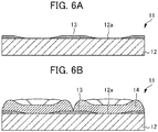
non-conductive film 13 on themetal plate 12, as with thecathode plate 11, include a method in which a thermosetting non-conductive resin such as an epoxy resin is applied onto the flat plate-shaped metal plate 12 by a screen printing method, and is heated, and thus, thenon-conductive film 13 having a desired pattern is formed, as illustrated inFig. 6A (refer toPatent Documents 1 and 2). Furthermore,Fig. 6B illustrates a state in which nickel (electric nickel) 14 is electrodeposited on theconductive section 12a by using thecathode plate 11 on which thenon-conductive film 13 is formed. In thecathode plate 11, thenickel 14 starts to be electrodeposited from theconductive section 12a, and grows not only in a thickness (vertical) direction but also in a planar (horizontal) direction, and thus, is in a state where thenickel 14 rises to the upper section of thenon-conductive film 13. - In addition, for example, as illustrated in
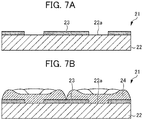
Fig. 7A , a method has been also proposed in which a photosensitive non-conductive resin is applied onto ametal plate 22, and is exposed and developed, and the non-conductive resin in a portion corresponding to aconductive section 22a is removed, and thus, anon-conductive film 23 having a desired pattern is formed. Furthermore,Fig. 7B illustrates a state in which the nickel (electric nickel) 24 is electrodeposited on theconductive section 22a by using thecathode plate 21 on which thenon-conductive film 23 is formed. Even in thecathode plate 21, thenickel 24 starts to be electrodeposited from theconductive section 22a, and grows not only in the thickness direction but also in the planar direction. - Further, a method has been also proposed in which the periphery of a metal structure that is incorporated such that a plurality of studs to be a conductive section are arranged at regular intervals is solidified with an insulating resin by an injection molding method, and thus, a cathode plate configuring a non-conductive section is manufactured (refer to Patent Document 3).
- Patent Document 1: Japanese Examined Patent Application Publication No.
S51-036693 - Patent Document 2: Japanese Unexamined Patent Application, Publication No.
S52-152832 - Patent Document 3: Japanese Examined Patent Application Publication No.
S56-029960 - In a case where the small mass-shaped electric nickel is manufactured by using the cathode plate as described above, it is required that the lifetime of the non-conductive film formed on the cathode plate (the non-conductive section) is long, and even in a case where the non-conductive film is lost (degraded), the maintenance can be easily performed.
- As illustrated in
Fig. 6A , in a case where thenon-conductive film 13 is formed by applying the non-conductive resin onto themetal plate 12 by screen printing, a film thickness of thenon-conductive film 13 gradually decreases as being close to theconductive section 12a, and thus, becomes extremely thin on the boundary with respect to theconductive section 12a. Such a change in the film thickness of thenon-conductive film 13 depends on a coating amount of the non-conductive resin, the viscosity of the non-conductive resin, temperature properties of the viscosity, a curing temperature of the non-conductive resin, surface roughness of a metal surface, surface free energy, and the like. For this reason, the film thickness of thenon-conductive film 13 becomes extremely thin on the boundary with respect to theconductive section 12a. - As described above, in a case where small mass-shaped electric nickel is manufactured by using the
cathode plate 11 as illustrated inFig. 5 andFig. 6 , thenickel 14 starts to be electrodeposited from theconductive section 12a, grows not only in the vertical direction but also in the horizontal direction, and thus, is in a state where thenickel 14 gradually rises to thenon-conductive film 13. For this reason, in the portion of the thinnon-conductive film 13 that is formed in the vicinity of the boundary with respect to theconductive section 12a, adhesiveness with respect to themetal plate 12 easily decreases due to the permeation of an electrolysis solution, and the non-conductive film is easily lost due to a stress at the time of electrodepositing thenickel 14 or an impact at the time of peeling off the electric nickel. In addition, in a case where thenon-conductive film 13 is lost once, thenon-conductive film 13 in the vicinity of the lost portion floats from the surface of themetal plate 12, and thus, the electrolysis solution more easily permeates through the gap, and as a result thereof, in the case of continuously electrodepositing nickel, the electrolysis solution is sunk into the gap of thenon-conductive film 13 that floats from the surface of themetal plate 12, and thus, thenickel 14 is electrodeposited. Then, in the case of peeling off thenickel 14 that is sunk into the gap and is electrodeposited, thenon-conductive film 13 that is bitten by thenickel 14 is further lost. - As described above, in the
cathode plate 11 of the related art, in a case where thenon-conductive film 13 is lost in a chain reaction, and the lost portion spreads, thenickels 14 grown from the adjacentconductive section 12a are easily joined to each other, and thus, it is not possible to obtain electric nickel having a desired shape, and a defective product is obtained. Therefore, it is necessary to maintain thecathode plate 11 by peeling off the entirenon-conductive film 13 before thenon-conductive film 13 is lost, and by forming again thenon-conductive film 13. However, in practice, it is necessary to maintain thecathode plate 11 in a step where an electrodeposition treatment of nickel is performed several times to less than 10 times at a maximum, and thus, not only does productivity decrease, but also a maintenance cost increases. - On the other hand, as illustrated in
Fig. 7A , in thecathode plate 21 on which thenon-conductive film 23 is formed by being exposed and developed by using the photosensitive non-conductive resin, it is possible to form thenon-conductive film 23 with a uniform film thickness. However, when thenickel 24 is peeled off after the electrodeposition, thenickel 24 is caught by a step of thenon-conductive film 23 configuring the convex section, and a large impact is easily applied to thenon-conductive film 23, and thus, thenon-conductive film 23 is lost. - Furthermore, as with
Patent Document 3, in the method of configuring the non-conductive section by injection molding, the lifetime of the non-conductive section to be formed is lengthened, but a manufacturing cost of the cathode plate itself increases, and thus, it is difficult to maintain the cathode plate in a case where the non-conductive section is degraded. - The present invention has been made in consideration of such circumstances of the related art, an object thereof is to provide a cathode plate for metal electrodeposition in which a non-conductive film on a metal plate is less likely to be lost, and thus, can be repeatedly used, and even in a case where the non-conductive film is lost, maintenance becomes easy, and a manufacturing method for the same.
- The present inventors have conducted intensive studies in order to solve the problems described above. As a result thereof, it has been found that a conductive section is formed by providing protrusions on a metal plate, and a non-conductive film is provided on a metal surface other than the protrusion, and thus, the non-conductive film is less likely to be lost. Further, it has been found that a side face of the protrusion has a predetermined shape, and thus, the non-conductive film is more effectively prevented from being lost, and even in a case where the non-conductive film is formed again, and thus, maintenance is necessary, the non-conductive film does not remain at the time of peeling off the non-conductive film, and the maintenance is easily performed, and the present invention has been completed.
- (1) A first invention of the present invention is a cathode plate for metal electrodeposition, including: a metal plate in which a plurality of disk-shaped protrusions are arranged on at least one surface; and a non-conductive film formed on a surface of the metal plate other than the protrusion, in which the protrusion has a side face that is in a shape formed of a substantially vertical section and an inclined section, a height L1 of the protrusion is greater than or equal to 50 µm and less than or equal to 1000 µm, and when an intersection between a vertical line vertically lowered from a position X that is 20 µm outward from an outer peripheral edge of the protrusion and the side face is defined as Y, a length L2 from X to Y is greater than or equal to 40 µm and less than or equal to 0.8 × L1 µm.
- (2) A second invention of the present invention is the cathode plate for metal electrodeposition in which the metal plate is formed of titanium or stainless steel, in the first invention.
- (3) A third invention of the present invention is the cathode plate for metal electrodeposition that is used for manufacturing electric nickel for plating, in the first invention or the second invention.
- (4) A fourth invention of the present invention is a manufacturing method of the cathode plate for metal electrodeposition according to any one of the first invention to the third invention, in which the plurality of disk-shaped protrusions are formed on at least one surface of the metal plate by wet etching processing or end mill processing.
- (5) A fifth invention of the present invention is the manufacturing method of the cathode plate for metal electrodeposition in which in the end mill processing, a radius end mill is used, in the fourth invention.
- According to the present invention, it is possible to provide a cathode plate for metal electrodeposition in which a non-conductive film is less likely to be lost, and thus, can be repeatedly used, and even in a case where the non-conductive film is lost, maintenance becomes easy, and a manufacturing method for the same.
-
-
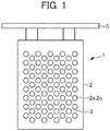
Fig. 1 is a plan view illustrating a configuration of a cathode plate. -
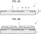
Fig. 2 is an enlarged sectional view of main parts illustrating the configuration of the cathode plate, in which -
Fig. 2A is an enlarged sectional view of main parts describing a state of the cathode plate before nickel electrodeposition, andFig. 2B is an enlarged sectional view of main parts describing a state of the cathode plate after the nickel electrodeposition. -
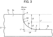
Fig. 3 is an enlarged sectional view of main parts enlarging an A section inFig. 2 , and is an enlarged sectional view of main parts describing a shape of a side face of a protrusion on a metal plate. -
Fig. 4 is an enlarged sectional view of main parts describing a manufacturing method of the cathode plate, in whichFig. 4A is an enlarged sectional view of main parts describing a first step, andFig. 4B is an enlarged sectional view of main parts describing a second step. -
Fig. 5 is a plan view illustrating a configuration of a cathode plate of the related art. -
Fig. 6 is an enlarged sectional view of main parts illustrating the configuration of the cathode plate of the related art, in whichFig. 6A is an enlarged sectional view of main parts describing a state of the cathode plate before the nickel electrodeposition,Fig. 6B is an enlarged sectional view of main parts describing a state of the cathode plate after the nickel electrodeposition. -
Fig. 7 is an enlarged sectional view of main parts illustrating the configuration of the cathode plate of the related art, in whichFig. 7A is an enlarged sectional view of main parts describing a state of the cathode plate before the nickel electrodeposition,Fig. 7B is an enlarged sectional view of main parts describing a state of the cathode plate after the nickel electrodeposition. - Hereinafter, an embodiment in which a cathode plate for metal electrodeposition of the present invention is applied to a cathode plate for metal electrodeposition that is used for manufacturing electric nickel (hereinafter, referred to as "this embodiment") will be described in detail. Furthermore, the present invention is not limited to the following embodiment, but can be suitably changed within a range not departing from the gist of the present invention.
- As illustrated in
Fig. 1 , acathode plate 1 according to this embodiment includes ametal plate 2 on which a plurality of disk-shapedprotrusions 2a are arranged and anon-conductive film 3 that is formed on a surface of themetal plate 2 other than theprotrusion 2a. As described below, for example, thecathode plate 1 is used by being hung in an electrolysis bath in which an electrolysis solution containing nickel or an anode is contained by a hangingmember 5, and nickel is electrodeposited on the surface into a desired shape. - As illustrated in
Fig. 1 andFig. 2A , themetal plate 2 is a flat plate-shaped metal plate, and includes the plurality of disk-shapedprotrusions 2a. Here, in themetal plate 2, the surface other than theprotrusion 2a is referred to as a "flat section 2b" with respect to theprotrusion 2a. In addition, a "height L1 of the protrusion" is a protruding height from the surface of theflat section 2b in themetal plate 2. - Furthermore, in
Fig. 2 , an example in which theprotrusions 2a are provided on one face of themetal plate 2 is illustrated, and theprotrusions 2a may be provided on both faces. - The size of the
metal plate 2 is not particularly limited, and may be suitably set in accordance with a desired size or the number of electric nickels to be manufactured. For example, the size of themetal plate 2 can be a rectangular size in which one side is greater than or equal to 100 mm and less than or equal to 2000 mm. In addition, in a case where theprotrusions 2a are provided on one surface, for example, it is preferable that the thickness of themetal plate 2 is approximately greater than 1.5 mm and less than or equal to 5 mm, and in a case where theprotrusions 2a are provided on both surfaces, for example, it is preferable that the thickness of the metal plate is approximately greater than or equal to 3 mm and less than or equal to 10 mm. In a case where the thickness of themetal plate 2 is excessively small, there is a tendency that warpage easily occurs by theprotrusion 2a and theflat section 2b. On the other hand, in a case where the thickness of themetal plate 2 is excessively large, the weight of themetal plate 2 increases, and thus, it is difficult to handle themetal plate 2. - The material of the
metal plate 2 is not particularly limited insofar as the material is a metal that is less corrosive with respect to an electrolysis solution to be used, and forms only loose adhesion with respect to an electrodeposition such as nickel, and examples of the material preferably include titanium and stainless steel. - In the
metal plate 2, the plurality of disk-shapedprotrusions 2a have a function as a conductive section by exposing the upper face from thenon-conductive film 3 described below, and theadjacent protrusions 2a form a concave step such that thenon-conductive film 3 is formed to have a predetermined thickness. Hereinafter, in theprotrusions 2a, the upper face exposed from thenon-conductive film 3 may be referred to as a "conductive section 2c". In theconductive section 2c,nickel 4 is electrodeposited by an electrolysis treatment. - The size of the disk-shaped
protrusion 2a may be suitably set in accordance with the size of desired electric nickel, and the diameter of the disk-shapedprotrusion 2a, for example, can be greater than or equal to 5 mm and less than or equal to 30 mm. In addition, the height L1 of theprotrusion 2a is preferably greater than or equal to 50 µm and less than or equal to 1000 µm, and is more preferably greater than or equal to 100 µm and less than or equal to 500 µm. In a case where the height L1 of theprotrusion 2a is excessively small, a film thickness of thenon-conductive film 3 that is formed on theflat section 2b of themetal plate 2 becomes insufficient, and thus, thenon-conductive film 3 is easily lost due to a stress at the time of electrodepositing thenickel 4 or an impact at the time of peeling off the electric nickel. On the other hand, in a case where the height L1 of theprotrusion 2a is excessively large, for example, when the non-conductive film is formed by screen printing, the number of times of performing coating increases, and thus, productivity decreases. In addition, in a case where the height L1 is excessively large, the distortion of themetal plate 2 easily occurs at the time of processing theprotrusion 2a, and themetal plate 2 is easily warped, and thus, it is difficult to form thenon-conductive film 3. Furthermore, in order to decrease the influence of the distortion of themetal plate 2, it is also possible to increase the thickness of themetal plate 2, but the weight of themetal plate 2 increases, and thus, it is difficult to handle themetal plate 2. - Here,
Fig. 3 is an enlarged sectional view of main parts enlarging an A section inFig. 2 , and is an enlarged sectional view of main parts describing the shape of the side face of the protrusion on the metal plate. As illustrated inFig. 3 , in themetal plate 2, the side face of theprotrusion 2a is in a shape formed of a substantiallyvertical section 2d and aninclined section 2e. Specifically, the substantiallyvertical section 2d is a portion that is substantially vertically formed with respect to the upper face formed of theconductive section 2c of theprotrusion 2a. In addition, theinclined section 2e is a portion that is formed by being inclined towardsflat section 2c from the substantiallyvertical section 2d. - As described above, the side face of the
protrusion 2a is configured to be in the shape formed of the substantiallyvertical section 2d and theinclined section 2e, and thus, even in a case where the electrodeposition treatment is repeatedly performed, it is possible to more effectively prevent thenon-conductive film 3 from being lost, and to repeatedly use thenon-conductive film 3. In addition, even in a case where thenon-conductive film 3 is formed again due to degradation such as the loss of thenon-conductive film 3, and thus, the maintenance is necessary, a phenomenon that thenon-conductive film 3 remains on the side face of theprotrusion 2a at the time of peeling off thenon-conductive film 3 from themetal plate 2, a so-called peeling residue is less likely to be generated, and thus, the maintenance becomes easy. - For example, in a case where the side face of the protrusion is in a shape formed only of the substantially vertical section without the inclined section, the non-conductive film easily remains on the corner of the side face of the protrusion that is formed at an approximately right angle, even in the case of peeling off the non-conductive film from the metal plate. On the other hand, in a case where the side face of the protrusion is in a shape formed only of the inclined section without the substantially vertical section, the non-conductive film in the vicinity of the conductive section becomes thin, and the degradation of the non-conductive film is accelerated, for example, the non-conductive film is easily lost by the electrodeposition treatment.
- More specifically, as illustrated in
Fig. 3 , in the shape of the side face of theprotrusion 2a, when an intersection between a vertically lowered line from a position X 20 µm outward from an outer peripheral edge of theprotrusion 2a and the side face of theprotrusion 2a is defined as Y, a length L2 from X to Y is greater than or equal to 40 µm, and is preferably greater than or equal to 100 µm. By setting the length L2 to be greater than or equal to 40 µm, even in a case where thenon-conductive film 3 that is formed on the metal plate 2 (theflat section 2b) is repeatedly subjected to the electrolysis treatment, thenon-conductive film 3 is less likely to be lost. Furthermore, here, the outer peripheral edge of theprotrusion 2a is an outer peripheral edge (an edge portion) of an upper face that is theconductive section 2c of theprotrusion 2a. - In addition, the length L2 is less than or equal to 0.8 times the height L1 of the
protrusion 2a (L1 × 0.8 µm). By setting the length L2 to be less than or equal to L1 × 0.8 µm, it is possible to effectively ensure theinclined section 2e, and as described above, the peeling residue of thenon-conductive film 3 is less likely to be generated on the side face of theprotrusion 2a, at the time of peeling off thenon-conductive film 3 from themetal plate 2. - Furthermore, the length L2 from X to Y corresponds to the height of the substantially
vertical section 2d, but it is not necessary that the intersection Y is a branch point from which the shape of the side face of theprotrusion 2a is obviously divided into the substantiallyvertical section 2d and theinclined section 2e. Hereinafter, there will be a case where the length L2 is referred to as the "height L2 of the substantiallyvertical section 2d". - In addition, a length L3 that is a difference between the height L1 of the
protrusion 2a and the length L2 is preferably greater than or equal to 10 µm, is more preferably greater than or equal to 25 µm and less than or equal to 0.7 × L1 µm. Hereinafter, there will be a case where the length L3 is referred to as the "height of theinclined section 2e". Further, when an intersection between a vertically lowered line from the intersection Y and a virtual face that is formed by extending the surface of theflat section 2b in a horizontal direction is defined as Y', a boundary position between theprotrusion 2a and theflat section 2b is defined as Z, and a length from Y' to Z is defined as L4, it is preferable that L3/L4 is greater than or equal to 0.2 and less than or equal to 1. Hereinafter, there will be a case where the length L4 is referred to as the "length L4 of theinclined section 2e". L3/L4 corresponds to an inclined angle of theinclined section 2e. - By setting the length L3 or L3/L4 to be in the range described above, even in a case where the
non-conductive film 3 is formed again, and thus, the maintenance is necessary, the peeling residue of thenon-conductive film 3 is less likely to be generated on the side face of theprotrusion 2a, at the time of peeling off thenon-conductive film 3 from themetal plate 2, and the maintenance becomes easy. - In addition, fine roughness may be provided on the surface of the
metal plate 2, that is, the upper face of the disk-shapedprotrusion 2a in themetal plate 2 by sandblasting or etching. Accordingly, thenickel 4 that is electrodeposited on theprotrusion 2a can be peeled off by a suitable impact without dropping out during the electrolysis treatment. In this case, it is preferable that the film thickness of thenon-conductive film 3 described below is greater than or equal to twice maximum surface roughness Rz of themetal plate 2. In a case where the film thickness of thenon-conductive film 3 is less than twice the maximum surface roughness Rz of themetal plate 2, there is a concern that a pinhole or an insulation failure portion is generated in thenon-conductive film 3. - As illustrated in
Fig. 2 , thenon-conductive film 3 is formed on theflat section 2b that is the surface of themetal plate 2 other than theprotrusion 2a, and thus, is in a state where the upper face of the plurality ofprotrusions 2a arranged on themetal plate 2, that is, theconductive section 2c is exposed. Then, thenickel 4 is electrodeposited in such aconductive section 2c of themetal plate 2, and thus, thenickel 4 is formed by being divided into each small mass. - The
non-conductive film 3 is formed on theflat section 2b on which the concave step formed by theadjacent protrusions 2a is provided. For this reason, in thenon-conductive film 3, the film thickness of the end section is less likely to be thin as with thenon-conductive film 13 of the related art illustrated inFig. 6 , and thus, thenon-conductive film 3 is less likely to be lost due to a stress at the time of electrodepositing thenickel 4 or an impact at the time of peeling off thenickel 4 after the electrodeposition. In addition, thenon-conductive film 3 does not concavely protrude as with thenon-conductive film 23 of the related art illustrated inFig. 7 , and thus, the end section is protected from the concave step. Accordingly, the impact of thenickel 4 that is applied to the end section of thenon-conductive film 3 is small even at the time of peeling off thenickel 4 from thecathode plate 1, and thus, thenon-conductive film 3 is less likely to be lost. As described above, in thecathode plate 1, thenon-conductive film 3 is less likely to be lost, and thus, it is possible to repeatedly use thenon-conductive film 3 in the electrodeposition without replacing thenon-conductive film 3, and it is possible to reduce a maintenance cost and to improve the productivity. - Furthermore, in a case where the
non-conductive film 3 is formed in theflat section 2b on themetal plate 2 by a screen printing method, the material of thenon-conductive film 3 is also applied onto the upper face of theprotrusion 2a, and thus, a surface area of theconductive section 2c may decrease, and an initial current density may increase, but there is no problem insofar as the properties of theelectrodeposited nickel 4 are not degraded. In addition, the film thickness of thenon-conductive film 3 attached onto the upper face of theprotrusion 2a is extremely thin, and thus, thenon-conductive film 3 is easily lost, but the film thickness of thenon-conductive film 3 that is formed on theflat section 2b is thick, and thus, thenon-conductive film 3 is prevented from being lost, and therefore, there is no problem. - The
non-conductive film 3 is not particularly limited insofar as the non-conductive film has non-conductivity, and is formed of a material that is less corrosive with respect to an electrolysis solution to be used. For example, it is preferable that thenon-conductive film 3 is configured of a thermosetting resin or a photocurable resin (an ultraviolet curable resin or the like), from the viewpoint of easy film formation. Specifically, an insulating resin such as an epoxy-based resin, a phenolic resin, a polyamide-based resin, a polyimide-based resin is exemplified. - In the
cathode plate 1 configured as described above, as illustrated inFig. 2B , the upper face of theprotrusion 2a that is exposed from thenon-conductive film 3 is theconductive section 2c, and thenickel 4 is electrodeposited. In thecathode plate 1, thenickel 4 grows not only in a thickness direction but also in a planar direction, and thus, is in a state where thenickel 4 rises to the upper section of thenon-conductive film 3. For this reason, it is preferable that the electrodeposition is ended before thenickels 4 grown from theconductive section 2c are in contact with each other in theadjacent protrusions 2a. - Then, the
nickel 4 is peeled off from thecathode plate 1 after the electrodeposition of thenickel 4 is ended, and thus, a plurality of small mass-shaped electric nickels can be obtained by onecathode plate 1. As described above, in thecathode plate 1 according to this embodiment, thenon-conductive film 3 is less likely to be lost, and thus, it is possible to repeatedly use thenon-conductive film 3 in the electrodeposition without replacing thenon-conductive film 3, and it is possible to reduce the maintenance cost and to improve the productivity. - Furthermore, in the
cathode plate 1 according to this embodiment, thenickel 4 is electrodeposited, but the present invention is not limited to nickel, and silver, gold, zinc, tin, chromium, cobalt, or an alloy thereof may be electrodeposited. - As illustrated in
Fig. 4 , a manufacturing method of thecathode plate 1 according to this embodiment includes a first step of forming the plurality of disk-shapedprotrusions 2a on at least one surface of the metal plate 2 (Fig. 4A ), and a second step of forming thenon-conductive film 3 on the surface of themetal plate 2 other than theprotrusion 2a (Fig. 4B ). - In the first step, the plurality of disk-shaped
protrusions 2a are formed on the surface of themetal plate 2. For example, a portion other than theprotrusions 2a is removed from the flat plate-shapedmetal plate 2 to leave theprotrusions 2a having the height L1, and thus, theflat section 2b is formed. As a processing method, wet etching processing or end mill processing is preferable, and the wet etching processing is more preferable in order to process a large area. - For example, in a case where the flat plate-shaped stainless steel plate is processed by wet etching, a photosensitive etching resist is applied onto a surface of a stainless steel plate, and then, is exposed through a film or glass on which desired pattern is drawn, the etching resist on a portion to be etched is removed by a development treatment. Then, the stainless steel plate subjected to the development treatment is applied to an etching solution (for example, a ferric chloride solution), a part of the stainless steel plate from which the etching resist is removed is removed, and finally, the etching resist is peeled off, and thus, the plurality of disk-shaped
protrusions 2a corresponding to a desired pattern can be formed. In the case of the wet etching, an etching rate with respect to stainless steel in a portion in the vicinity of the resist is slower than an etching rate with respect to stainless steel in a portion separated from a resist end section, and thus, a sectional shape of theprotrusion 2a is a shape formed of the substantiallyvertical section 2d and theinclined section 2e. In addition, it is possible to process a large area at one time, and thus, it is possible to perform the production for a short period of time. - On the other hand, in the case of the end mill processing, the
metal plate 2 is processed by a radius end mill having a desired shape in which a tip end of a blade of a drill is rounded, and thus, the substantiallyvertical section 2d and theinclined section 2e can be more precisely formed. - Furthermore, the
protrusion 2a may be formed on only one surface of themetal plate 2, or may be formed on both surfaces of themetal plate 2. - In the second step, the
non-conductive film 3 is formed on theflat section 2b that is the surface of themetal plate 2 other than theprotrusion 2a. A formation method of thenon-conductive film 3 is not particularly limited, and thenon-conductive film 3 can be formed by screen printing. In a case where the material of thenon-conductive film 3 is a thermosetting resin or a photocurable resin, as necessary, thermal curing or photo curing may be performed. - According to the manufacturing method of the cathode plate according to this embodiment, it is possible to obtain the
cathode plate 1 in which thenon-conductive film 3 on themetal plate 2 is less likely to be lost, and thus, can be repeatedly used, by a simple method described above. In addition, even in a case where thenon-conductive film 3 is formed again due to degradation such as the loss of thenon-conductive film 3, and thus, the maintenance is necessary, the peeling residue of thenon-conductive film 3 is less likely to be generated on the side face of theprotrusion 2a, at the time of peeling off thenon-conductive film 3, and the maintenance is easy. - Hereinafter, examples of the present invention will be described in more detail, but the present invention is not limited to the examples. Furthermore, for the sake of convenience, the description will be given by applying the same reference numerals to members having the same functions as those of the members illustrated in
Fig. 1 to Fig. 6 . - The
cathode plate 1 as illustrated inFig. 1 andFig. 2 was prepared. Specifically, first, themetal plate 2 of stainless steel (a cold rolling material) having a size of 200 mm × 100 mm × 4 mm was subjected to wet etching, and thus, the (18) disk-shapedprotrusions 2a were formed. At this time, in the size of theprotrusion 2a, the diameter was 14 mm, the height L1 was 300 µm, and a minimum distance between centers of theadjacent protrusions 2a was 21 mm. The shape was measured by a laser displacement meter, and thus, the height L2 of the substantiallyvertical section 2d was 120 µm on average, the height L3 of theinclined section 2e was 180 µm on average, and the length L4 of theinclined section 2e was 420 µm on average. - Next, a thermosetting epoxy resin was applied onto the
flat section 2b of themetal plate 2 by a screen printing method, and was cured by being heated at 150°C for 60 minutes, and thus, thenon-conductive film 3 was formed. - The
cathode plate 1 was prepared as with Example 1, except that the height L1 of theprotrusion 2a of themetal plate 2 was 500 µm. In thecathode plate 1 prepared as described above, the height L2 of the substantiallyvertical section 2d was measured by the laser displacement meter, and thus, was 200 µm on average, the height L3 of theinclined section 2e was 300 µm on average, and the length L4 of theinclined section 2e was 650 µm on average. - The
cathode plate 1 was prepared as with Example 1, except that the height L1 of theprotrusion 2a of themetal plate 2 was 60 µm. In thecathode plate 1 prepared as described above, the height L2 of the substantiallyvertical section 2d was measured by the laser displacement meter, and thus, was 45 µm on average, the height L3 of theinclined section 2e was 15 µm on average, and the length L4 of theinclined section 2e was 20 µm on average. - The
cathode plate 1 was prepared as with Example 1, except that the height L1 of theprotrusion 2a of themetal plate 2 was 200 µm. In thecathode plate 1 prepared as described above, the height L2 of the substantiallyvertical section 2d was measured by the laser displacement meter, and thus, was 90 µm on average, the height L3 of theinclined section 2e was 110 µm on average, and the length L4 of theinclined section 2e was 240 µm on average. - The
cathode plate 1 was prepared as with Example 1, except that the disk-shaped protrusion was formed by using a radius end mill drill. In thecathode plate 1 prepared as described above, the height L2 of the substantiallyvertical section 2d was measured by the laser displacement meter, and thus, was 100 µm on average, the height L3 of theinclined section 2e was 200 µm on average, and the length L4 of theinclined section 2e was 220 µm on average. - In Comparative Example 1, the
cathode plate 11 of the related art as illustrated inFig. 5 andFig. 6 was prepared. Specifically, a thermosetting epoxy resin was applied onto the flat plate-shapedmetal plate 12 of stainless steel (a cold rolling material) having a size of 200 mm × 100 mm × 4 mm by a screen printing method while leaving the (18)conductive sections 12a having a diameter of 14 mm, and was cured by being heated at 150°C for 60 minutes, and thus, thenon-conductive film 13 was formed, and thecathode plate 11 was prepared. - The
cathode plate 1 was prepared as with Example 1, except that the height L1 of theprotrusion 2a of themetal plate 2 was 40 µm. In thecathode plate 1 prepared as described above, the height L2 of the substantiallyvertical section 2d was measured by the laser displacement meter, and thus, was 30 µm on average, the height L3 of theinclined section 2e was 10 µm on average, and the length L4 of theinclined section 2e was 50 µm on average. - The
cathode plate 1 was prepared as with Example 4, except that themetal plate 2 of stainless steel (a hot rolling material) having a size of 200 mm × 100 mm × 4 mm was used. In thecathode plate 1 prepared as described above, the height L2 of the substantiallyvertical section 2d was measured by the laser displacement meter, and thus, a part thereof was approximately 20 µm, the height L3 of theinclined section 2e was 180 µm on average, and the length L4 of theinclined section 2e was 300 µm on average. Such a portion in which the height L2 of the substantiallyvertical section 2d is low is formed by a concave section of surface roughness that is formed in the manufacturing step of the hot rolling material. - The
cathode plate 1 was prepared as with Example 4, except that the disk-shapedprotrusion 2a was formed by using a flat end mill drill. In thecathode plate 1 prepared as described above, the height L2 of the substantiallyvertical section 2d was measured by the laser displacement meter, and thus, was 200 µm, and there was no inclined section. - As with Example 1, the metal plate was subjected to the wet etching, and protrusions of which the height L1 was 2000 µm were formed. However, the warpage of the metal plate was large, and it was difficult to form the non-conductive film by screen printing.
- The electric nickel was manufactured by an electrolysis treatment, by using the cathode plate prepared in each of the examples and each of the comparative examples. Specifically, the cathode plate, and an anode plate of electric nickel having a size of 200 mm × 100 mm × 10 mm were immersed in an electrolysis bath containing a nickel chloride electrolysis solution to face each other. Then, nickel was electrodeposited on the surface of the cathode plate, in a condition of an initial current density of 710 A/m2 and an electrolysis time for 3 days. The electric nickel precipitated on the cathode plate was peeled off after the electrolysis, and thus, small mass-shaped electric nickel for plating was obtained.
- The number of times that the cathode plate used in the electrolysis treatment can be directly repeatedly used was evaluated. In a case where the loss of the non-conductive film spreads, the adjacent protrusions, and the nickels electrodeposited on the conductive section are joined to each to each other, and thus, electric nickel having desired shape may not be obtained. Therefore, in a case where the non-conductive film was lost over greater than or equal to 1 mm from the boundary with respect to the protrusion in a flat section direction, the use was stopped, and the number of repeating times up to that time point was evaluated. In addition, the electrodeposition and the peeling of nickel were repeated up to 20 times. In addition, even in a case where the non-conductive film was lost and the diameter of the conductive section was enlarged by greater than or equal to 1 mm, the use was stopped, and the number of repeating times up to that time point was evaluated.
- The non-conductive film of the cathode plate of which the number of repeating times was evaluated was peeled off by a waterjet, and peeling properties of the non-conductive film were evaluated. Specifically, a rotary nozzle of which a hole diameter was 0.4 mm and the number of holes was 3 was used as the waterjet, and the non-conductive film was peeled off at a hydraulic pressure of 200 MPa, the quantity of water of 10 L/minute, and an effective width of 30 mm, while moving the nozzle at 2 m/minute. In the peeling properties of the non-conductive film, a case where the non-conductive film was capable of being approximately completely removed within approximately 20 seconds per one cathode plate (200 mm × 100 mm) was evaluated as "Excellent" and a case where the non-conductive film was not capable of being removed even after 20 seconds was evaluated as "Peeling Residue Occurs".
- In Table 1, an evaluation result is shown along with the configuration of the cathode plate.
[Table 1] Cathode plate material Processing method Shape of cathode plate L1 (µm) L2 (µm) L3 (µm) L4 (µm) L3/L4 Number of repeating times Peeling properties of non-conductive film Example 1 Cold rolling material Wet etching With projection 300 120 180 420 0.43 >20 Excellent Example 2 Cold rolling material Wet etching With projection 500 200 300 650 0.46 >20 Excellent Example 3 Cold rolling material Wet etching With projection 60 45 15 20 0.75 16 Excellent Example 4 Cold rolling material Wet etching With projection 200 90 110 240 0.46 >20 Excellent Example 5 Cold rolling material End mill With projection 300 100 200 220 0.91 >20 Excellent Comparative Example 1 Cold rolling material - Plate shape - - - - - 7 Excellent Comparative Example 2 Cold rolling material Wet etching With projection 40 30 10 50 0.2 9 Excellent Comparative Example 3 Hot rolling material Wet etching With projection 200 20 180 300 0.6 10 Excellent Comparative Example 4 Cold rolling material End mill With projection 200 200 - - - >20 Peeling residue Comparative Example 5 Cold rolling material Wet etching With projection 2000 - - - - (Difficult to print non-conductive film due to large warpage) - As shown in Table 1, in Examples 1 to 5 using the
cathode plate 1 in which thenon-conductive film 3 was formed on theflat section 2b of themetal plate 2, and the height L1 of theprotrusion 2a was greater than or equal to 60 µm and less than or equal to 500 µm, the loss of thenon-conductive film 3 was suppressed, and thus, was capable of being sufficiently repeatedly used. In particular, in Examples 1, 2, 4, and 5 in which the height L1 of theprotrusion 2a was greater than or equal to 100 µm, the number of times that thenon-conductive film 3 was capable of being repeatedly used was greater than 20 times. In addition, in Examples 1 to 5 in which the height L2 of the substantiallyvertical section 2d was greater than or equal to 40 µm and less than or equal to 0.8 × L1 µm, when thenon-conductive film 3 was peeled off by the waterjet, thenon-conductive film 3 was capable of being excellently peeled off without generating a peeling residue or the like. - On the other hand, in Comparative Example 1 in which the
non-conductive film 13 was formed on the flat plate-shapedmetal plate 12, thenon-conductive film 14 was lost, and thus, was not capable of being sufficiently repeatedly used. In addition, in Comparative Example 2 in which the height L1 of theprotrusion 2a was low, thenon-conductive film 3 was lost, and thus, was not capable of being sufficiently repeatedly used. In addition, in Comparative Example 3, thenon-conductive film 3 is lost from a portion in which the height L2 of the substantiallyvertical section 2d was as low as 20 µm, in the shape of the side face of theprotrusion 2a, and thus, was not capable of being sufficiently repeatedly used. In Comparative Example 4, there was no inclined section in the shape of the side face of theprotrusion 2a, and thus, when thenon-conductive film 3 was peeled off by the waterjet, a peeling residue was generated on the corner of the side face of theprotrusion 2a that was formed at an approximately right angle. Further, in Comparative Example 5, the height L1 of theprotrusion 2a was excessively high, and thus, warpage of themetal plate 2 was large, it was difficult to perform coating with respect to the non-conductive film, and thus, it was not possible to configure the cathode plate. -
- 1
- CATHODE PLATE
- 2
- METAL PLATE
- 2a
- PROTRUSION
- 2b
- FLAT SECTION
- 2c
- CONDUCTIVE SECTION
- 2d
- SUBSTANTIALLY VERTICAL SECTION
- 2e
- INCLINED SECTION
- 3
- NON-CONDUCTIVE FILM
- 4
- NICKEL
Claims (5)
- A cathode plate for metal electrodeposition, comprising:a metal plate in which a plurality of disk-shaped protrusions are arranged on at least one surface; anda non-conductive film formed on a surface of the metal plate other than the protrusion,wherein the protrusion has a side face that is in a shape formed of a substantially vertical section and an inclined section,a height L1 of the protrusion is greater than or equal to 50 µm and less than or equal to 1000 µm, andwhen an intersection between a vertical line vertically lowered from a position X that is 20 µm outward from an outer peripheral edge of the protrusion and the side face is defined as Y, a length L2 from X to Y is greater than or equal to 40 µm and less than or equal to 0.8 × L1 µm.
- The cathode plate for metal electrodeposition according to claim 1,
wherein the metal plate is formed of titanium or stainless steel. - The cathode plate for metal electrodeposition according to claim 1 or 2,
wherein the cathode plate for metal electrodeposition is used for manufacturing electric nickel for plating. - A manufacturing method of the cathode plate for metal electrodeposition according to any one of claims 1 to 3,
wherein the plurality of disk-shaped protrusions are formed on at least one surface of the metal plate by wet etching processing or end mill processing. - The manufacturing method of the cathode plate for metal electrodeposition according to claim 4,
wherein in the end mill processing, a radius end mill is used.
Applications Claiming Priority (2)
| Application Number | Priority Date | Filing Date | Title |
|---|---|---|---|
| JP2017105796A JP6500937B2 (en) | 2017-05-29 | 2017-05-29 | Negative electrode plate for metal electrodeposition and method of manufacturing the same |
| PCT/JP2018/013187 WO2018220979A1 (en) | 2017-05-29 | 2018-03-29 | Cathode plate for metal electrodeposition and manufacturing method for same |
Publications (3)
| Publication Number | Publication Date |
|---|---|
| EP3633074A1 true EP3633074A1 (en) | 2020-04-08 |
| EP3633074A4 EP3633074A4 (en) | 2021-03-10 |
| EP3633074B1 EP3633074B1 (en) | 2022-10-05 |
Family
ID=64454726
Family Applications (1)
| Application Number | Title | Priority Date | Filing Date |
|---|---|---|---|
| EP18809926.1A Active EP3633074B1 (en) | 2017-05-29 | 2018-03-29 | Cathode plate for metal electrodeposition and manufacturing method for same |
Country Status (5)
| Country | Link |
|---|---|
| EP (1) | EP3633074B1 (en) |
| JP (1) | JP6500937B2 (en) |
| CN (1) | CN110546310B (en) |
| CA (1) | CA3064525C (en) |
| WO (1) | WO2018220979A1 (en) |
Families Citing this family (6)
| Publication number | Priority date | Publication date | Assignee | Title |
|---|---|---|---|---|
| JP7188219B2 (en) * | 2019-03-25 | 2022-12-13 | 住友金属鉱山株式会社 | Cathode plate for metal electrodeposition |
| JP7188216B2 (en) * | 2019-03-25 | 2022-12-13 | 住友金属鉱山株式会社 | Manufacturing method of cathode plate for metal electrodeposition |
| JP7188218B2 (en) * | 2019-03-25 | 2022-12-13 | 住友金属鉱山株式会社 | Cathode plate for metal electrodeposition |
| JP7238524B2 (en) * | 2019-03-25 | 2023-03-14 | 住友金属鉱山株式会社 | Cathode plate for metal electrodeposition |
| JP7188217B2 (en) * | 2019-03-25 | 2022-12-13 | 住友金属鉱山株式会社 | Manufacturing method of cathode plate for metal electrodeposition |
| JP2021095594A (en) * | 2019-12-13 | 2021-06-24 | 住友金属鉱山株式会社 | Production method of button-type electric nickel |
Family Cites Families (9)
| Publication number | Priority date | Publication date | Assignee | Title |
|---|---|---|---|---|
| US3668081A (en) * | 1971-03-17 | 1972-06-06 | Int Nickel Co | Production of electrolytic metal |
| GB1573449A (en) * | 1976-04-01 | 1980-08-20 | Falconbridge Nickel Mines Ltd | Reusable electrolysis cathode |
| US4040915A (en) * | 1976-06-15 | 1977-08-09 | The International Nickel Company, Inc. | Method for producing regular electronickel or S nickel rounds from electroplating baths giving highly stressed deposits |
| JPS6038678Y2 (en) * | 1981-05-15 | 1985-11-19 | 住友金属鉱山株式会社 | Mother plate for metal electrodeposition |
| JPH10317197A (en) * | 1997-05-14 | 1998-12-02 | Sumitomo Metal Mining Co Ltd | Electric nickel for plating, cathode plate for manufacturing the same, and manufacturing method |
| KR20030023640A (en) * | 2000-06-30 | 2003-03-19 | 허니웰 인터내셔널 인코포레이티드 | Method and apparatus for processing metals, and the metals so produced |
| WO2010028428A1 (en) * | 2008-09-09 | 2010-03-18 | Steelmore Holdings Pty Ltd | A cathode and a method of forming a cathode |
| KR101664540B1 (en) * | 2014-04-02 | 2016-10-25 | 오씨아이 주식회사 | Electrolytic plating electrode and plating apparatus comprising thereof |
| US10676831B2 (en) * | 2014-07-15 | 2020-06-09 | De Nora Permelec Ltd | Electrolysis cathode and method for producing electrolysis cathode |
-
2017
- 2017-05-29 JP JP2017105796A patent/JP6500937B2/en active Active
-
2018
- 2018-03-29 WO PCT/JP2018/013187 patent/WO2018220979A1/en not_active Ceased
- 2018-03-29 CA CA3064525A patent/CA3064525C/en active Active
- 2018-03-29 EP EP18809926.1A patent/EP3633074B1/en active Active
- 2018-03-29 CN CN201880026566.8A patent/CN110546310B/en active Active
Also Published As
| Publication number | Publication date |
|---|---|
| JP2018199857A (en) | 2018-12-20 |
| WO2018220979A1 (en) | 2018-12-06 |
| EP3633074A4 (en) | 2021-03-10 |
| CA3064525C (en) | 2020-03-24 |
| CA3064525A1 (en) | 2018-12-06 |
| CN110546310A (en) | 2019-12-06 |
| JP6500937B2 (en) | 2019-04-17 |
| EP3633074B1 (en) | 2022-10-05 |
| CN110546310B (en) | 2020-09-15 |
Similar Documents
| Publication | Publication Date | Title |
|---|---|---|
| EP3633074B1 (en) | Cathode plate for metal electrodeposition and manufacturing method for same | |
| CN102149855B (en) | Electroforming method | |
| EP3489395A1 (en) | Metal electrodeposition cathode plate and production method therefor | |
| KR101889165B1 (en) | Deposition mask, method for preparing the same and method for preparing organic electroluminescent device using the deposition mask | |
| MY144932A (en) | Production apparatus for electro-deposited metal foil, production method of thin plate insoluble metal electrode used in production apparatus for electro-deposited metal foil, and electro-deposited metal foil produced by using production apparatus for electro-deposited metal foil | |
| US20200095697A1 (en) | Manufacturing Apparatus of Electrolytic Copper Foil | |
| JP6638589B2 (en) | Cathode plate for metal electrodeposition and method for producing the same | |
| KR101879080B1 (en) | Apparatus for preparing fe-ni alloy foil | |
| US3695927A (en) | Electrodeposition process for producing perforated foils with raised portions at the edges of the holes | |
| KR101282327B1 (en) | Method for manufacturing film with metal fine pattern | |
| CN101713086B (en) | Mould for electroplating connector terminal | |
| JP7188217B2 (en) | Manufacturing method of cathode plate for metal electrodeposition | |
| JP7188216B2 (en) | Manufacturing method of cathode plate for metal electrodeposition | |
| JP7188218B2 (en) | Cathode plate for metal electrodeposition | |
| JP7238524B2 (en) | Cathode plate for metal electrodeposition | |
| JP7188219B2 (en) | Cathode plate for metal electrodeposition | |
| JP6737036B2 (en) | Metal electrodeposited cathode plate and method for producing the same | |
| JP6737035B2 (en) | Metal electrodeposited cathode plate and method for producing the same | |
| US8012329B2 (en) | Dimensional control in electroforms | |
| CN113416924B (en) | Mask, method for manufacturing mask, and master mold for manufacturing mask | |
| JP6760191B2 (en) | Manufacturing method of specially shaped electrodeposition | |
| TW202120328A (en) | Hole structure and manufacturing method thereof, and different material joint structure and manufacturing method thereof | |
| CN103938230A (en) | Manufacturing method for light guide plate mold insert | |
| KR102325255B1 (en) | Mask and producing method of the same | |
| JP2003082491A (en) | Micro electroforming mold and its manufacturing method |
Legal Events
| Date | Code | Title | Description |
|---|---|---|---|
| STAA | Information on the status of an ep patent application or granted ep patent |
Free format text: STATUS: THE INTERNATIONAL PUBLICATION HAS BEEN MADE |
|
| PUAI | Public reference made under article 153(3) epc to a published international application that has entered the european phase |
Free format text: ORIGINAL CODE: 0009012 |
|
| STAA | Information on the status of an ep patent application or granted ep patent |
Free format text: STATUS: REQUEST FOR EXAMINATION WAS MADE |
|
| 17P | Request for examination filed |
Effective date: 20191218 |
|
| AK | Designated contracting states |
Kind code of ref document: A1 Designated state(s): AL AT BE BG CH CY CZ DE DK EE ES FI FR GB GR HR HU IE IS IT LI LT LU LV MC MK MT NL NO PL PT RO RS SE SI SK SM TR |
|
| AX | Request for extension of the european patent |
Extension state: BA ME |
|
| DAV | Request for validation of the european patent (deleted) | ||
| DAX | Request for extension of the european patent (deleted) | ||
| A4 | Supplementary search report drawn up and despatched |
Effective date: 20210208 |
|
| RIC1 | Information provided on ipc code assigned before grant |
Ipc: C25C 7/02 20060101AFI20210202BHEP Ipc: C25D 17/12 20060101ALI20210202BHEP Ipc: C25D 1/20 20060101ALI20210202BHEP Ipc: C23F 1/02 20060101ALI20210202BHEP Ipc: C25D 17/16 20060101ALI20210202BHEP Ipc: C25C 1/08 20060101ALI20210202BHEP Ipc: C25D 1/00 20060101ALI20210202BHEP |
|
| STAA | Information on the status of an ep patent application or granted ep patent |
Free format text: STATUS: EXAMINATION IS IN PROGRESS |
|
| 17Q | First examination report despatched |
Effective date: 20211104 |
|
| RIC1 | Information provided on ipc code assigned before grant |
Ipc: C23F 1/04 20060101ALI20220524BHEP Ipc: C25D 17/16 20060101ALI20220524BHEP Ipc: C25D 1/20 20060101ALI20220524BHEP Ipc: C25D 1/00 20060101ALI20220524BHEP Ipc: C25D 17/12 20060101ALI20220524BHEP Ipc: C25C 1/08 20060101ALI20220524BHEP Ipc: C23F 1/02 20060101ALI20220524BHEP Ipc: C25C 7/02 20060101AFI20220524BHEP |
|
| GRAP | Despatch of communication of intention to grant a patent |
Free format text: ORIGINAL CODE: EPIDOSNIGR1 |
|
| STAA | Information on the status of an ep patent application or granted ep patent |
Free format text: STATUS: GRANT OF PATENT IS INTENDED |
|
| INTG | Intention to grant announced |
Effective date: 20220704 |
|
| GRAS | Grant fee paid |
Free format text: ORIGINAL CODE: EPIDOSNIGR3 |
|
| GRAA | (expected) grant |
Free format text: ORIGINAL CODE: 0009210 |
|
| STAA | Information on the status of an ep patent application or granted ep patent |
Free format text: STATUS: THE PATENT HAS BEEN GRANTED |
|
| AK | Designated contracting states |
Kind code of ref document: B1 Designated state(s): AL AT BE BG CH CY CZ DE DK EE ES FI FR GB GR HR HU IE IS IT LI LT LU LV MC MK MT NL NO PL PT RO RS SE SI SK SM TR |
|
| REG | Reference to a national code |
Ref country code: GB Ref legal event code: FG4D |
|
| REG | Reference to a national code |
Ref country code: CH Ref legal event code: EP |
|
| REG | Reference to a national code |
Ref country code: AT Ref legal event code: REF Ref document number: 1522807 Country of ref document: AT Kind code of ref document: T Effective date: 20221015 |
|
| REG | Reference to a national code |
Ref country code: IE Ref legal event code: FG4D |
|
| REG | Reference to a national code |
Ref country code: DE Ref legal event code: R096 Ref document number: 602018041478 Country of ref document: DE |
|
| REG | Reference to a national code |
Ref country code: NO Ref legal event code: T2 Effective date: 20221005 |
|
| REG | Reference to a national code |
Ref country code: LT Ref legal event code: MG9D |
|
| REG | Reference to a national code |
Ref country code: NL Ref legal event code: MP Effective date: 20221005 |
|
| REG | Reference to a national code |
Ref country code: AT Ref legal event code: MK05 Ref document number: 1522807 Country of ref document: AT Kind code of ref document: T Effective date: 20221005 |
|
| PG25 | Lapsed in a contracting state [announced via postgrant information from national office to epo] |
Ref country code: NL Free format text: LAPSE BECAUSE OF FAILURE TO SUBMIT A TRANSLATION OF THE DESCRIPTION OR TO PAY THE FEE WITHIN THE PRESCRIBED TIME-LIMIT Effective date: 20221005 |
|
| PG25 | Lapsed in a contracting state [announced via postgrant information from national office to epo] |
Ref country code: SE Free format text: LAPSE BECAUSE OF FAILURE TO SUBMIT A TRANSLATION OF THE DESCRIPTION OR TO PAY THE FEE WITHIN THE PRESCRIBED TIME-LIMIT Effective date: 20221005 Ref country code: PT Free format text: LAPSE BECAUSE OF FAILURE TO SUBMIT A TRANSLATION OF THE DESCRIPTION OR TO PAY THE FEE WITHIN THE PRESCRIBED TIME-LIMIT Effective date: 20230206 Ref country code: LT Free format text: LAPSE BECAUSE OF FAILURE TO SUBMIT A TRANSLATION OF THE DESCRIPTION OR TO PAY THE FEE WITHIN THE PRESCRIBED TIME-LIMIT Effective date: 20221005 Ref country code: FI Free format text: LAPSE BECAUSE OF FAILURE TO SUBMIT A TRANSLATION OF THE DESCRIPTION OR TO PAY THE FEE WITHIN THE PRESCRIBED TIME-LIMIT Effective date: 20221005 Ref country code: ES Free format text: LAPSE BECAUSE OF FAILURE TO SUBMIT A TRANSLATION OF THE DESCRIPTION OR TO PAY THE FEE WITHIN THE PRESCRIBED TIME-LIMIT Effective date: 20221005 Ref country code: AT Free format text: LAPSE BECAUSE OF FAILURE TO SUBMIT A TRANSLATION OF THE DESCRIPTION OR TO PAY THE FEE WITHIN THE PRESCRIBED TIME-LIMIT Effective date: 20221005 |
|
| PG25 | Lapsed in a contracting state [announced via postgrant information from national office to epo] |
Ref country code: RS Free format text: LAPSE BECAUSE OF FAILURE TO SUBMIT A TRANSLATION OF THE DESCRIPTION OR TO PAY THE FEE WITHIN THE PRESCRIBED TIME-LIMIT Effective date: 20221005 Ref country code: PL Free format text: LAPSE BECAUSE OF FAILURE TO SUBMIT A TRANSLATION OF THE DESCRIPTION OR TO PAY THE FEE WITHIN THE PRESCRIBED TIME-LIMIT Effective date: 20221005 Ref country code: LV Free format text: LAPSE BECAUSE OF FAILURE TO SUBMIT A TRANSLATION OF THE DESCRIPTION OR TO PAY THE FEE WITHIN THE PRESCRIBED TIME-LIMIT Effective date: 20221005 Ref country code: IS Free format text: LAPSE BECAUSE OF FAILURE TO SUBMIT A TRANSLATION OF THE DESCRIPTION OR TO PAY THE FEE WITHIN THE PRESCRIBED TIME-LIMIT Effective date: 20230205 Ref country code: HR Free format text: LAPSE BECAUSE OF FAILURE TO SUBMIT A TRANSLATION OF THE DESCRIPTION OR TO PAY THE FEE WITHIN THE PRESCRIBED TIME-LIMIT Effective date: 20221005 Ref country code: GR Free format text: LAPSE BECAUSE OF FAILURE TO SUBMIT A TRANSLATION OF THE DESCRIPTION OR TO PAY THE FEE WITHIN THE PRESCRIBED TIME-LIMIT Effective date: 20230106 |
|
| REG | Reference to a national code |
Ref country code: DE Ref legal event code: R097 Ref document number: 602018041478 Country of ref document: DE |
|
| PG25 | Lapsed in a contracting state [announced via postgrant information from national office to epo] |
Ref country code: SM Free format text: LAPSE BECAUSE OF FAILURE TO SUBMIT A TRANSLATION OF THE DESCRIPTION OR TO PAY THE FEE WITHIN THE PRESCRIBED TIME-LIMIT Effective date: 20221005 Ref country code: RO Free format text: LAPSE BECAUSE OF FAILURE TO SUBMIT A TRANSLATION OF THE DESCRIPTION OR TO PAY THE FEE WITHIN THE PRESCRIBED TIME-LIMIT Effective date: 20221005 Ref country code: EE Free format text: LAPSE BECAUSE OF FAILURE TO SUBMIT A TRANSLATION OF THE DESCRIPTION OR TO PAY THE FEE WITHIN THE PRESCRIBED TIME-LIMIT Effective date: 20221005 Ref country code: DK Free format text: LAPSE BECAUSE OF FAILURE TO SUBMIT A TRANSLATION OF THE DESCRIPTION OR TO PAY THE FEE WITHIN THE PRESCRIBED TIME-LIMIT Effective date: 20221005 Ref country code: CZ Free format text: LAPSE BECAUSE OF FAILURE TO SUBMIT A TRANSLATION OF THE DESCRIPTION OR TO PAY THE FEE WITHIN THE PRESCRIBED TIME-LIMIT Effective date: 20221005 |
|
| PLBE | No opposition filed within time limit |
Free format text: ORIGINAL CODE: 0009261 |
|
| STAA | Information on the status of an ep patent application or granted ep patent |
Free format text: STATUS: NO OPPOSITION FILED WITHIN TIME LIMIT |
|
| PG25 | Lapsed in a contracting state [announced via postgrant information from national office to epo] |
Ref country code: SK Free format text: LAPSE BECAUSE OF FAILURE TO SUBMIT A TRANSLATION OF THE DESCRIPTION OR TO PAY THE FEE WITHIN THE PRESCRIBED TIME-LIMIT Effective date: 20221005 Ref country code: AL Free format text: LAPSE BECAUSE OF FAILURE TO SUBMIT A TRANSLATION OF THE DESCRIPTION OR TO PAY THE FEE WITHIN THE PRESCRIBED TIME-LIMIT Effective date: 20221005 |
|
| 26N | No opposition filed |
Effective date: 20230706 |
|
| REG | Reference to a national code |
Ref country code: DE Ref legal event code: R119 Ref document number: 602018041478 Country of ref document: DE |
|
| PG25 | Lapsed in a contracting state [announced via postgrant information from national office to epo] |
Ref country code: MC Free format text: LAPSE BECAUSE OF FAILURE TO SUBMIT A TRANSLATION OF THE DESCRIPTION OR TO PAY THE FEE WITHIN THE PRESCRIBED TIME-LIMIT Effective date: 20221005 |
|
| REG | Reference to a national code |
Ref country code: CH Ref legal event code: PL |
|
| GBPC | Gb: european patent ceased through non-payment of renewal fee |
Effective date: 20230329 |
|
| PG25 | Lapsed in a contracting state [announced via postgrant information from national office to epo] |
Ref country code: SI Free format text: LAPSE BECAUSE OF FAILURE TO SUBMIT A TRANSLATION OF THE DESCRIPTION OR TO PAY THE FEE WITHIN THE PRESCRIBED TIME-LIMIT Effective date: 20221005 |
|
| REG | Reference to a national code |
Ref country code: BE Ref legal event code: MM Effective date: 20230331 |
|
| PG25 | Lapsed in a contracting state [announced via postgrant information from national office to epo] |
Ref country code: LU Free format text: LAPSE BECAUSE OF NON-PAYMENT OF DUE FEES Effective date: 20230329 |
|
| REG | Reference to a national code |
Ref country code: IE Ref legal event code: MM4A |
|
| PG25 | Lapsed in a contracting state [announced via postgrant information from national office to epo] |
Ref country code: GB Free format text: LAPSE BECAUSE OF NON-PAYMENT OF DUE FEES Effective date: 20230329 |
|
| PG25 | Lapsed in a contracting state [announced via postgrant information from national office to epo] |
Ref country code: LI Free format text: LAPSE BECAUSE OF NON-PAYMENT OF DUE FEES Effective date: 20230331 Ref country code: IE Free format text: LAPSE BECAUSE OF NON-PAYMENT OF DUE FEES Effective date: 20230329 Ref country code: GB Free format text: LAPSE BECAUSE OF NON-PAYMENT OF DUE FEES Effective date: 20230329 Ref country code: FR Free format text: LAPSE BECAUSE OF NON-PAYMENT OF DUE FEES Effective date: 20230331 Ref country code: DE Free format text: LAPSE BECAUSE OF NON-PAYMENT OF DUE FEES Effective date: 20231003 Ref country code: CH Free format text: LAPSE BECAUSE OF NON-PAYMENT OF DUE FEES Effective date: 20230331 |
|
| PG25 | Lapsed in a contracting state [announced via postgrant information from national office to epo] |
Ref country code: BE Free format text: LAPSE BECAUSE OF NON-PAYMENT OF DUE FEES Effective date: 20230331 |
|
| PG25 | Lapsed in a contracting state [announced via postgrant information from national office to epo] |
Ref country code: IT Free format text: LAPSE BECAUSE OF FAILURE TO SUBMIT A TRANSLATION OF THE DESCRIPTION OR TO PAY THE FEE WITHIN THE PRESCRIBED TIME-LIMIT Effective date: 20221005 |
|
| PG25 | Lapsed in a contracting state [announced via postgrant information from national office to epo] |
Ref country code: BG Free format text: LAPSE BECAUSE OF FAILURE TO SUBMIT A TRANSLATION OF THE DESCRIPTION OR TO PAY THE FEE WITHIN THE PRESCRIBED TIME-LIMIT Effective date: 20221005 |
|
| PG25 | Lapsed in a contracting state [announced via postgrant information from national office to epo] |
Ref country code: BG Free format text: LAPSE BECAUSE OF FAILURE TO SUBMIT A TRANSLATION OF THE DESCRIPTION OR TO PAY THE FEE WITHIN THE PRESCRIBED TIME-LIMIT Effective date: 20221005 |
|
| PG25 | Lapsed in a contracting state [announced via postgrant information from national office to epo] |
Ref country code: CY Free format text: LAPSE BECAUSE OF FAILURE TO SUBMIT A TRANSLATION OF THE DESCRIPTION OR TO PAY THE FEE WITHIN THE PRESCRIBED TIME-LIMIT; INVALID AB INITIO Effective date: 20180329 |
|
| PG25 | Lapsed in a contracting state [announced via postgrant information from national office to epo] |
Ref country code: HU Free format text: LAPSE BECAUSE OF FAILURE TO SUBMIT A TRANSLATION OF THE DESCRIPTION OR TO PAY THE FEE WITHIN THE PRESCRIBED TIME-LIMIT; INVALID AB INITIO Effective date: 20180329 |
|
| PG25 | Lapsed in a contracting state [announced via postgrant information from national office to epo] |
Ref country code: TR Free format text: LAPSE BECAUSE OF FAILURE TO SUBMIT A TRANSLATION OF THE DESCRIPTION OR TO PAY THE FEE WITHIN THE PRESCRIBED TIME-LIMIT Effective date: 20221005 |
|
| PGFP | Annual fee paid to national office [announced via postgrant information from national office to epo] |
Ref country code: NO Payment date: 20260310 Year of fee payment: 9 |