EP3627543A1 - Method for manufacturing tft substrate - Google Patents
Method for manufacturing tft substrate Download PDFInfo
- Publication number
- EP3627543A1 EP3627543A1 EP17909921.3A EP17909921A EP3627543A1 EP 3627543 A1 EP3627543 A1 EP 3627543A1 EP 17909921 A EP17909921 A EP 17909921A EP 3627543 A1 EP3627543 A1 EP 3627543A1
- Authority
- EP
- European Patent Office
- Prior art keywords
- layer
- graphene
- insulation layer
- metal foil
- substrate manufacturing
- Prior art date
- Legal status (The legal status is an assumption and is not a legal conclusion. Google has not performed a legal analysis and makes no representation as to the accuracy of the status listed.)
- Granted
Links
Images






Classifications
-
- H—ELECTRICITY
- H10—SEMICONDUCTOR DEVICES; ELECTRIC SOLID-STATE DEVICES NOT OTHERWISE PROVIDED FOR
- H10D—INORGANIC ELECTRIC SEMICONDUCTOR DEVICES
- H10D30/00—Field-effect transistors [FET]
- H10D30/01—Manufacture or treatment
-
- H—ELECTRICITY
- H10—SEMICONDUCTOR DEVICES; ELECTRIC SOLID-STATE DEVICES NOT OTHERWISE PROVIDED FOR
- H10D—INORGANIC ELECTRIC SEMICONDUCTOR DEVICES
- H10D30/00—Field-effect transistors [FET]
- H10D30/01—Manufacture or treatment
- H10D30/021—Manufacture or treatment of FETs having insulated gates [IGFET]
- H10D30/031—Manufacture or treatment of FETs having insulated gates [IGFET] of thin-film transistors [TFT]
-
- H—ELECTRICITY
- H10—SEMICONDUCTOR DEVICES; ELECTRIC SOLID-STATE DEVICES NOT OTHERWISE PROVIDED FOR
- H10D—INORGANIC ELECTRIC SEMICONDUCTOR DEVICES
- H10D30/00—Field-effect transistors [FET]
- H10D30/40—FETs having zero-dimensional [0D], one-dimensional [1D] or two-dimensional [2D] charge carrier gas channels
- H10D30/47—FETs having zero-dimensional [0D], one-dimensional [1D] or two-dimensional [2D] charge carrier gas channels having two-dimensional [2D] charge carrier gas channels, e.g. nanoribbon FETs or high electron mobility transistors [HEMT]
-
- H—ELECTRICITY
- H10—SEMICONDUCTOR DEVICES; ELECTRIC SOLID-STATE DEVICES NOT OTHERWISE PROVIDED FOR
- H10D—INORGANIC ELECTRIC SEMICONDUCTOR DEVICES
- H10D30/00—Field-effect transistors [FET]
- H10D30/60—Insulated-gate field-effect transistors [IGFET]
- H10D30/67—Thin-film transistors [TFT]
- H10D30/6729—Thin-film transistors [TFT] characterised by the electrodes
- H10D30/6737—Thin-film transistors [TFT] characterised by the electrodes characterised by the electrode materials
- H10D30/6739—Conductor-insulator-semiconductor electrodes
-
- H—ELECTRICITY
- H10—SEMICONDUCTOR DEVICES; ELECTRIC SOLID-STATE DEVICES NOT OTHERWISE PROVIDED FOR
- H10D—INORGANIC ELECTRIC SEMICONDUCTOR DEVICES
- H10D30/00—Field-effect transistors [FET]
- H10D30/60—Insulated-gate field-effect transistors [IGFET]
- H10D30/67—Thin-film transistors [TFT]
- H10D30/674—Thin-film transistors [TFT] characterised by the active materials
- H10D30/6741—Group IV materials, e.g. germanium or silicon carbide
-
- H—ELECTRICITY
- H10—SEMICONDUCTOR DEVICES; ELECTRIC SOLID-STATE DEVICES NOT OTHERWISE PROVIDED FOR
- H10D—INORGANIC ELECTRIC SEMICONDUCTOR DEVICES
- H10D30/00—Field-effect transistors [FET]
- H10D30/60—Insulated-gate field-effect transistors [IGFET]
- H10D30/67—Thin-film transistors [TFT]
- H10D30/6757—Thin-film transistors [TFT] characterised by the structure of the channel, e.g. transverse or longitudinal shape or doping profile
-
- H—ELECTRICITY
- H10—SEMICONDUCTOR DEVICES; ELECTRIC SOLID-STATE DEVICES NOT OTHERWISE PROVIDED FOR
- H10D—INORGANIC ELECTRIC SEMICONDUCTOR DEVICES
- H10D30/00—Field-effect transistors [FET]
- H10D30/60—Insulated-gate field-effect transistors [IGFET]
- H10D30/67—Thin-film transistors [TFT]
- H10D30/6758—Thin-film transistors [TFT] characterised by the insulating substrates
-
- H—ELECTRICITY
- H10—SEMICONDUCTOR DEVICES; ELECTRIC SOLID-STATE DEVICES NOT OTHERWISE PROVIDED FOR
- H10D—INORGANIC ELECTRIC SEMICONDUCTOR DEVICES
- H10D62/00—Semiconductor bodies, or regions thereof, of devices having potential barriers
- H10D62/10—Shapes, relative sizes or dispositions of the regions of the semiconductor bodies; Shapes of the semiconductor bodies
- H10D62/117—Shapes of semiconductor bodies
- H10D62/118—Nanostructure semiconductor bodies
-
- H—ELECTRICITY
- H10—SEMICONDUCTOR DEVICES; ELECTRIC SOLID-STATE DEVICES NOT OTHERWISE PROVIDED FOR
- H10D—INORGANIC ELECTRIC SEMICONDUCTOR DEVICES
- H10D62/00—Semiconductor bodies, or regions thereof, of devices having potential barriers
- H10D62/80—Semiconductor bodies, or regions thereof, of devices having potential barriers characterised by the materials
- H10D62/83—Semiconductor bodies, or regions thereof, of devices having potential barriers characterised by the materials being Group IV materials, e.g. B-doped Si or undoped Ge
- H10D62/8303—Diamond
-
- H—ELECTRICITY
- H10—SEMICONDUCTOR DEVICES; ELECTRIC SOLID-STATE DEVICES NOT OTHERWISE PROVIDED FOR
- H10D—INORGANIC ELECTRIC SEMICONDUCTOR DEVICES
- H10D62/00—Semiconductor bodies, or regions thereof, of devices having potential barriers
- H10D62/80—Semiconductor bodies, or regions thereof, of devices having potential barriers characterised by the materials
- H10D62/881—Semiconductor bodies, or regions thereof, of devices having potential barriers characterised by the materials being a two-dimensional material
- H10D62/882—Graphene
-
- H—ELECTRICITY
- H10—SEMICONDUCTOR DEVICES; ELECTRIC SOLID-STATE DEVICES NOT OTHERWISE PROVIDED FOR
- H10D—INORGANIC ELECTRIC SEMICONDUCTOR DEVICES
- H10D64/00—Electrodes of devices having potential barriers
- H10D64/01—Manufacture or treatment
- H10D64/011—Manufacture or treatment of electrodes ohmically coupled to a semiconductor
- H10D64/0111—Manufacture or treatment of electrodes ohmically coupled to a semiconductor to Group IV semiconductors
- H10D64/0114—Manufacture or treatment of electrodes ohmically coupled to a semiconductor to Group IV semiconductors to diamond, semiconducting diamond-like carbon or graphene
-
- H—ELECTRICITY
- H10—SEMICONDUCTOR DEVICES; ELECTRIC SOLID-STATE DEVICES NOT OTHERWISE PROVIDED FOR
- H10D—INORGANIC ELECTRIC SEMICONDUCTOR DEVICES
- H10D64/00—Electrodes of devices having potential barriers
- H10D64/01—Manufacture or treatment
- H10D64/013—Manufacture or treatment of electrodes having a conductor capacitively coupled to a semiconductor by an insulator
- H10D64/01364—Manufacture or treatment of electrodes having a conductor capacitively coupled to a semiconductor by an insulator the semiconductor being diamond, semiconducting diamond-like carbon or graphene
-
- H—ELECTRICITY
- H10—SEMICONDUCTOR DEVICES; ELECTRIC SOLID-STATE DEVICES NOT OTHERWISE PROVIDED FOR
- H10D—INORGANIC ELECTRIC SEMICONDUCTOR DEVICES
- H10D86/00—Integrated devices formed in or on insulating or conducting substrates, e.g. formed in silicon-on-insulator [SOI] substrates or on stainless steel or glass substrates
- H10D86/01—Manufacture or treatment
- H10D86/021—Manufacture or treatment of multiple TFTs
- H10D86/0231—Manufacture or treatment of multiple TFTs using masks, e.g. half-tone masks
-
- B—PERFORMING OPERATIONS; TRANSPORTING
- B82—NANOTECHNOLOGY
- B82Y—SPECIFIC USES OR APPLICATIONS OF NANOSTRUCTURES; MEASUREMENT OR ANALYSIS OF NANOSTRUCTURES; MANUFACTURE OR TREATMENT OF NANOSTRUCTURES
- B82Y10/00—Nanotechnology for information processing, storage or transmission, e.g. quantum computing or single electron logic
-
- H—ELECTRICITY
- H10—SEMICONDUCTOR DEVICES; ELECTRIC SOLID-STATE DEVICES NOT OTHERWISE PROVIDED FOR
- H10D—INORGANIC ELECTRIC SEMICONDUCTOR DEVICES
- H10D86/00—Integrated devices formed in or on insulating or conducting substrates, e.g. formed in silicon-on-insulator [SOI] substrates or on stainless steel or glass substrates
- H10D86/40—Integrated devices formed in or on insulating or conducting substrates, e.g. formed in silicon-on-insulator [SOI] substrates or on stainless steel or glass substrates characterised by multiple TFTs
- H10D86/411—Integrated devices formed in or on insulating or conducting substrates, e.g. formed in silicon-on-insulator [SOI] substrates or on stainless steel or glass substrates characterised by multiple TFTs characterised by materials, geometry or structure of the substrates
-
- H—ELECTRICITY
- H10—SEMICONDUCTOR DEVICES; ELECTRIC SOLID-STATE DEVICES NOT OTHERWISE PROVIDED FOR
- H10D—INORGANIC ELECTRIC SEMICONDUCTOR DEVICES
- H10D86/00—Integrated devices formed in or on insulating or conducting substrates, e.g. formed in silicon-on-insulator [SOI] substrates or on stainless steel or glass substrates
- H10D86/40—Integrated devices formed in or on insulating or conducting substrates, e.g. formed in silicon-on-insulator [SOI] substrates or on stainless steel or glass substrates characterised by multiple TFTs
- H10D86/60—Integrated devices formed in or on insulating or conducting substrates, e.g. formed in silicon-on-insulator [SOI] substrates or on stainless steel or glass substrates characterised by multiple TFTs wherein the TFTs are in active matrices
Definitions
- the present invention relates to the field of display technology, and more particular to a thin-film transistor (TFT) substrate manufacturing method.
- TFT thin-film transistor
- pixels are each driven by a thin-film transistor (TFT) integrated therewith on the back side in order to achieve a desired screen displaying effect of high speed, high brightness, and high contrast.
- TFTs that are commonly available are made up of three electrodes of gate, source, and drain, an insulation layer, and a semiconductor layer.
- Graphene is the thinnest and toughest nanometer material that is currently known in the world and is one of the hot spots of study and research due to excellent conductivity adjustability, mechanical properties, and thermal conductivity. Being a novel material that is extremely thin and has extremely high electrical conductivity, graphene has greater potential for application in electronic elements and transistors. Graphene is reportedly having extremely low sheet resistance (less than 100 ⁇ / ⁇ ), but can become a wide-band two-dimensional insulation material after being subjected to doping. Thus, having been treated properly, graphene may show property of n type or p type semiconductor and can be used in TFT devices of the display business.
- a technique that is commonly used and may provide better performance of graphene is chemical vapor deposition (CVD).
- CVD chemical vapor deposition
- a process involving such a technique to fabricate a TFT device is first depositing, through CVD, graphene on a metal base, such as copper and nickel, followed by etching off the metal base to obtain a graphene film, and then transferring the graphene film, through a roll-to-roll process or other processes, to a base on which a desired film has been deposited for being assembled into a TFT device.
- a metal base such as copper and nickel
- An objective of the present invention is to provide a thin film transistor (TFT) substrate manufacturing method, which lowers down manufacturing costs, simplifies operations, and reducing the number of mask involved.
- TFT thin film transistor
- the present invention provides a TFT substrate manufacturing method, which comprises the following steps:
- the metal foil is made of a material of copper or nickel.
- Step S1 the operation of changing graphene band gap involves chemical doping, wherein chemical doping is conducted on the graphene film at the same time of deposition thereof so that graphene so deposited is a doped graphene film so as to obtain the graphene semiconductor active layer; or, alternatively, the operation of changing graphene band gap involves photolithography, wherein, after the deposition of the graphene film, the graphene film is cut into thin ribbons to form graphene nanoribbon, so as to obtain the graphene semiconductor active layer.
- Step S1 plasma enhanced chemical vapor deposition is used to deposit the graphene film, and the graphene film so deposited is a single-layered graphene film; and the graphene semiconductor active layer has a bang gap that is greater than 0.1 eV.
- Step S2 chemical vapor deposition is used to deposit and form the inorganic insulation layer, and the inorganic insulation layer is made of a material comprising silicon nitride, silicon oxide, diyttrium trioxide, or hafnium dioxide.
- Step S3 the organic base is formed through solution coating and curing and the organic base is made of a material of polydimethylsiloxane.
- Step S5 a wet etching operation is applied to subject the metal foil to etching.
- Step S6 a coating operation is applied to form the organic insulation layer, and the organic insulation layer is made of a material of polymethylmethacrylate.
- Step S6 physical vapor deposition is applied deposit and form the gate electrode conductor layer, and the gate electrode conductor layer is made of a material comprising aluminum, copper, or indium tin oxide.
- the TFT substrate manufacturing method further comprises Step S8 of providing a reinforcement base and melting the organic base for attaching to the reinforcement base; wherein the reinforcement base comprises glass, a plastic material of polyethylene terephthalate, or a silicon plate.
- the present invention also provides a TFT substrate manufacturing method, which comprises the following steps:
- the efficacy of the present invention is that the present invention provides a TFT substrate manufacturing method, which comprises first depositing a graphene film on a metal foil, followed by applying an operation of changing graphene bang gap to form a graphene semiconductor active layer, and then, sequentially forming an inorganic insulation layer and an organic base on the graphene semiconductor active layer, wherein through an operation turning up-side down, the metal foil is set on a topmost layer, followed by forming a photoresist layer, through a patterning operation, on the metal foil, subjecting the metal foil to etching with the photoresist layer serving as a shielding layer to form a source electrode and a drain electrode, and then, sequentially forming an organic insulation layer and a gate electrode conductor layer on the photoresist layer and the graphene semiconductor active layer, and finally, applying a photoresist peeling agent to remove the photoresist layer with portions of the organic insulation layer and the gate electrode conductor layer located on the photoresist layer being simultaneously therewith to
- the manufacturing method involves an operation of turning up-side down to to allow the metal foil that is used to deposit a graphene film to be re-used as an electrode material for formation of the source and drain electrodes so that an effect of lowering down manufacturing cost and simplifying operations can be achieved. And, through application of lift-off technique, only one mask is necessary to obtain patterned source electrode, drain electrode, and gate electrode.
- the present invention provides a TFT substrate manufacturing method, which comprises the following steps: Step S1: as shown in FIG. 2 , providing a metal foil 100', depositing a graphene film on the metal foil 100', and applying an operation of changing graphene band gap to obtain a graphene semiconductor active layer 200.
- the metal foil 100' is made of a material that serves as a material of a base for forming, through deposition, the graphene film and also possesses electrical conductivity to serve, subsequently, a material of an electrode, such as a metal material, including copper (Cu) or nickel (Ni).
- a metal material including copper (Cu) or nickel (Ni).
- the operation of changing graphene band gap involves chemical doping, which is, specifically, conducting chemical doping to the graphene film at the same time of deposition thereof so that the graphene film so deposited is a doped graphene film so as to obtain the graphene semiconductor active layer 200; or, alternatively, the operation of changing graphene band gap involves photolithography, which is, specifically, cutting, after the deposition of the graphene film, the graphene film into thin ribbons to form graphene nanoribbon (GNR), so as to obtain the graphene semiconductor active layer 200.
- chemical doping is, specifically, conducting chemical doping to the graphene film at the same time of deposition thereof so that the graphene film so deposited is a doped graphene film so as to obtain the graphene semiconductor active layer 200
- photolithography which is, specifically, cutting, after the deposition of the graphene film, the graphene film into thin ribbons to form graphene nanoribbon (GNR), so as to obtain the graphene semiconductor active layer 200
- the graphene semiconductor active layer 200 so obtained has a bang gap that is greater than 0.1 eV.
- Step S1 plasma enhanced chemical vapor deposition (PECVD) is used to deposit the graphene film, and the graphene film so deposited is preferably a single-layered graphene film having a thickness that is preferably less than 5 nm.
- PECVD plasma enhanced chemical vapor deposition
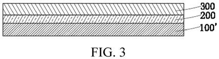
- Step S2 as shown in FIG. 3 , forming, through deposition, an inorganic insulation layer 300 on the graphene semiconductor active layer 200 in order to provide protection to the graphene semiconductor active layer 200 for preventing influence caused by an organic base, which is formed subsequently, on the graphene semiconductor active layer 200.
- Step S2 chemical vapor deposition (CVD) is used to deposit and form the inorganic insulation layer 300, and the inorganic insulation layer 300 is made of material that comprises an inorganic material, including for example silicon nitride (SiNx), silicon oxide (Si02), diyttrium trioxide, and hafnium dioxide (Hf02).
- CVD chemical vapor deposition
- Step S3 as shown in FIG. 4 , forming an organic base 400 on the inorganic insulation layer 300 to form a primary structure.
- the organic base 400 is formed through solution coating and curing and the organic base 400 is made of a material that can be polydimethylsiloxane (PDMS).
- PDMS polydimethylsiloxane
- Step S4 as shown in FIG. 5 , turning up-side down the primary structure formed in Step S3 to set the organic base 400 as a bottommost layer and the metal foil 100' as a topmost layer, and forming a photoresist (PR) layer 500, through a patterning operation with a mask, on the metal foil 100'.
- PR photoresist
- the patterning operation specifically comprises a coating step, an exposure step, and a development step that are carried out in sequence.
- Step S5 as shown in FIG. 6 , subjecting the metal foil 100' to etching by using the photoresist layer 500 as a shielding layer so as to form a source electrode 110 and a drain electrode 120 that are spaced from each other.
- Step S5 a wet etching operation is applied to subject the metal foil 100' to etching.
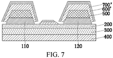
- Step S6 as shown in FIG. 7 , forming an organic insulation layer 600' on the photoresist layer 500 and the graphene semiconductor active layer 200, and forming, through deposition, a gate electrode conductor layer 700' on the organic insulation layer 600'.
- Step S6 a coating operation is applied to form the organic insulation layer 600', and the organic insulation layer 600' can be formed on the photoresist layer 500 at a low temperature.
- the organic insulation layer 600' has a dielectric constant that is three times of the dielectric constant of vacuum, such as having a material of polymethylmethacrylate (PMMA).
- Step S6 physical vapor deposition (PVD) is used to deposit and form the gate electrode conductor layer 700', and the gate electrode conductor layer 700' is made of a material that is a metal or oxide having electrical conductivity, such as aluminum (Al), copper, and indium tin oxide (ITO).
- PVD physical vapor deposition
- Al aluminum
- ITO indium tin oxide
- Step S7 as shown in FIG. 8 , applying a photoresist peeling agent to remove the photoresist layer 500 and also to have portions of the organic insulation layer 600' and the gate electrode conductor layer 700' that are located on the photoresist layer 500 removed simultaneously with the photoresist layer 500 such that a gate insulation layer 600 is obtained with a remaining portion of the organic insulation layer 600' so as to be located on the graphene semiconductor active layer 200 and between the source electrode 110 and the drain electrode 120 and a gate electrode 700 is obtained with a remaining portion of the gate electrode conductor layer 700' so as to be located on the gate insulation layer 600.
- the organic base 400 functions as a base that is located on the outermost side to provide a support to a TFT device and is made of a material that is resistant to acid, alkali, and water and can be selected as PDMS or other materials that can be formed through solution coating process.
- the TFT substrate manufacturing method according to the present invention may further comprises Step S8: as shown in FIG. 9 , providing a reinforcement base 800 and melting the organic base 400 for attaching to the reinforcement base 800.
- the reinforcement base 800 can be made of glass, a plastic material of polyethylene terephthalate (PET), or a silicon plate.
- PET polyethylene terephthalate
- an operation of tuning up-side down is involved to allow a metal foil 100' that is used to deposit a graphene film to be re-used as an electrode material for formation of source and drain electrodes 110, 120 so that an effect of lowering down manufacturing cost and simplifying operations can be achieved. And, through application of lift-off technique, only one mask is necessary to obtain patterned source electrode 110, drain electrode 120, and gate electrode 700.
- the present invention provides a TFT substrate manufacturing method, which comprises first depositing a graphene film on a metal foil, followed by applying an operation of changing graphene bang gap to form a graphene semiconductor active layer, and then, sequentially forming an inorganic insulation layer and an organic base on the graphene semiconductor active layer, wherein through an operation turning up-side down, the metal foil is set on a topmost layer, followed by forming a photoresist layer, through a patterning operation, on the metal foil, subjecting the metal foil to etching with the photoresist layer serving as a shielding layer to form a source electrode and a drain electrode, and then, sequentially forming an organic insulation layer and a gate electrode conductor layer on the photoresist layer and the graphene semiconductor active layer, and finally, applying a photoresist peeling agent to remove the photoresist layer with portions of the organic insulation layer and the gate electrode conductor layer located on the photoresist layer being simultaneously therewith to thereby form patterned gate insulation layer
- the manufacturing method involves an operation of turning up-side down to to allow the metal foil that is used to deposit a graphene film to be re-used as an electrode material for formation of the source and drain electrodes so that an effect of lowering down manufacturing cost and simplifying operations can be achieved. And, through application of lift-off technique, only one mask is necessary to obtain patterned source electrode, drain electrode, and gate electrode.
Landscapes
- Thin Film Transistor (AREA)
- Electrodes Of Semiconductors (AREA)
Abstract
Description
- The present invention relates to the field of display technology, and more particular to a thin-film transistor (TFT) substrate manufacturing method.
- In the active matrix display technology, pixels are each driven by a thin-film transistor (TFT) integrated therewith on the back side in order to achieve a desired screen displaying effect of high speed, high brightness, and high contrast. TFTs that are commonly available are made up of three electrodes of gate, source, and drain, an insulation layer, and a semiconductor layer.
- Graphene is the thinnest and toughest nanometer material that is currently known in the world and is one of the hot spots of study and research due to excellent conductivity adjustability, mechanical properties, and thermal conductivity. Being a novel material that is extremely thin and has extremely high electrical conductivity, graphene has greater potential for application in electronic elements and transistors. Graphene is reportedly having extremely low sheet resistance (less than 100 Ω/□), but can become a wide-band two-dimensional insulation material after being subjected to doping. Thus, having been treated properly, graphene may show property of n type or p type semiconductor and can be used in TFT devices of the display business. Contemporarily, for fabrication of large-area graphene, a technique that is commonly used and may provide better performance of graphene is chemical vapor deposition (CVD). A process involving such a technique to fabricate a TFT device is first depositing, through CVD, graphene on a metal base, such as copper and nickel, followed by etching off the metal base to obtain a graphene film, and then transferring the graphene film, through a roll-to-roll process or other processes, to a base on which a desired film has been deposited for being assembled into a TFT device. Such a process suffers various disadvantages, such as long cycle time, complicated operations, and increased expenditure for the metal base.
- Thus, it is very important to develop a manufacturing method for graphene-contained TFT substrates with simple operations and low cost.
- An objective of the present invention is to provide a thin film transistor (TFT) substrate manufacturing method, which lowers down manufacturing costs, simplifies operations, and reducing the number of mask involved.
- To achieve the above objective, the present invention provides a TFT substrate manufacturing method, which comprises the following steps:
- Step S1: providing a metal foil, depositing a graphene film on the metal foil, and applying an operation of changing graphene band gap to obtain a graphene semiconductor active layer;
- Step S2: forming, through deposition, an inorganic insulation layer on the graphene semiconductor active layer;
- Step S3: forming an organic base on the inorganic insulation layer to form a primary structure;
- Step S4: turning up-side down the primary structure formed in Step S3 to set the organic base as a bottommost layer and the metal foil as a topmost layer, and forming a photoresist layer, through a patterning operation with a mask, on the metal foil;
- Step S5: subjecting the metal foil to etching by using the photoresist layer as a shielding layer so as to form a source electrode and a drain electrode that are spaced from each other;
- Step S6: forming an organic insulation layer on the photoresist layer and the graphene semiconductor active layer, and forming, through deposition, a gate electrode conductor layer on the organic insulation layer; and
- Step S7: applying a photoresist peeling agent to remove the photoresist layer and also to have portions of the organic insulation layer and the gate electrode conductor layer that are located on the photoresist layer removed simultaneously with the photoresist layer such that a gate insulation layer is obtained with a remaining portion of the organic insulation layer so as to be located on the graphene semiconductor active layer and between the source electrode and the drain electrode and a gate electrode is obtained with a remaining portion of the gate electrode conductor layer so as to be located on the gate insulation layer.
- The metal foil is made of a material of copper or nickel.
- In Step S1, the operation of changing graphene band gap involves chemical doping, wherein chemical doping is conducted on the graphene film at the same time of deposition thereof so that graphene so deposited is a doped graphene film so as to obtain the graphene semiconductor active layer; or, alternatively,
the operation of changing graphene band gap involves photolithography, wherein, after the deposition of the graphene film, the graphene film is cut into thin ribbons to form graphene nanoribbon, so as to obtain the graphene semiconductor active layer. - In Step S1, plasma enhanced chemical vapor deposition is used to deposit the graphene film, and the graphene film so deposited is a single-layered graphene film; and the graphene semiconductor active layer has a bang gap that is greater than 0.1 eV.
- In Step S2, chemical vapor deposition is used to deposit and form the inorganic insulation layer, and the inorganic insulation layer is made of a material comprising silicon nitride, silicon oxide, diyttrium trioxide, or hafnium dioxide.
- In Step S3, the organic base is formed through solution coating and curing and the organic base is made of a material of polydimethylsiloxane.
- In Step S5, a wet etching operation is applied to subject the metal foil to etching.
- In Step S6, a coating operation is applied to form the organic insulation layer, and the organic insulation layer is made of a material of polymethylmethacrylate.
- In Step S6, physical vapor deposition is applied deposit and form the gate electrode conductor layer, and the gate electrode conductor layer is made of a material comprising aluminum, copper, or indium tin oxide.
- The TFT substrate manufacturing method further comprises Step S8 of providing a reinforcement base and melting the organic base for attaching to the reinforcement base;
wherein the reinforcement base comprises glass, a plastic material of polyethylene terephthalate, or a silicon plate. - The present invention also provides a TFT substrate manufacturing method, which comprises the following steps:
- Step S1: providing a metal foil, depositing a graphene film on the metal foil, and applying an operation of changing graphene band gap to obtain a graphene semiconductor active layer;
- Step S2: forming, through deposition, an inorganic insulation layer on the graphene semiconductor active layer;
- Step S3: forming an organic base on the inorganic insulation layer to form a primary structure;
- Step S4: turning up-side down the primary structure formed in Step S3 to set the organic base as a bottommost layer and the metal foil as a topmost layer, and forming a photoresist layer, through a patterning operation with a mask, on the metal foil;
- Step S5: subjecting the metal foil to etching by using the photoresist layer as a shielding layer so as to form a source electrode and a drain electrode that are spaced from each other;
- Step S6: forming an organic insulation layer on the photoresist layer and the graphene semiconductor active layer, and forming, through deposition, a gate electrode conductor layer on the organic insulation layer; and
- Step S7: applying a photoresist peeling agent to remove the photoresist layer and also to have portions of the organic insulation layer and the gate electrode conductor layer that are located on the photoresist layer removed simultaneously with the photoresist layer such that a gate insulation layer is obtained with a remaining portion of the organic insulation layer so as to be located on the graphene semiconductor active layer and between the source electrode and the drain electrode and a gate electrode is obtained with a remaining portion of the gate electrode conductor layer so as to be located on the gate insulation layer;
- The efficacy of the present invention is that the present invention provides a TFT substrate manufacturing method, which comprises first depositing a graphene film on a metal foil, followed by applying an operation of changing graphene bang gap to form a graphene semiconductor active layer, and then, sequentially forming an inorganic insulation layer and an organic base on the graphene semiconductor active layer, wherein through an operation turning up-side down, the metal foil is set on a topmost layer, followed by forming a photoresist layer, through a patterning operation, on the metal foil, subjecting the metal foil to etching with the photoresist layer serving as a shielding layer to form a source electrode and a drain electrode, and then, sequentially forming an organic insulation layer and a gate electrode conductor layer on the photoresist layer and the graphene semiconductor active layer, and finally, applying a photoresist peeling agent to remove the photoresist layer with portions of the organic insulation layer and the gate electrode conductor layer located on the photoresist layer being simultaneously therewith to thereby form patterned gate insulation layer and gate electrode. The manufacturing method involves an operation of turning up-side down to to allow the metal foil that is used to deposit a graphene film to be re-used as an electrode material for formation of the source and drain electrodes so that an effect of lowering down manufacturing cost and simplifying operations can be achieved. And, through application of lift-off technique, only one mask is necessary to obtain patterned source electrode, drain electrode, and gate electrode.
- For better understanding of the features and technical contents of the present invention, reference will be made to the following detailed description of the present invention and the attached drawings. However, the drawings are provided only for reference and illustration and are not intended to limit the present invention.
- The technical solution, as well as other beneficial advantages, of the present invention will become apparent from the following detailed description of embodiments of the present invention, with reference to the attached drawings. In the drawings:
-
FIG. 1 is a flow chart illustrating a thin-film transistor (TFT) substrate manufacturing method according to the present invention; -
FIG. 2 is a schematic view illustrating Step S1 of the TFT substrate manufacturing method according to the present invention; -
FIG. 3 is a schematic view illustrating Step S2 of the TFT substrate manufacturing method according to the present invention; -
FIG. 4 is a schematic view illustrating Step S3 of the TFT substrate manufacturing method according to the present invention; -
FIG. 5 is a schematic view illustrating Step S4 of the TFT substrate manufacturing method according to the present invention; -
FIG. 6 is a schematic view illustrating Step S5 of the TFT substrate manufacturing method according to the present invention; -
FIG. 7 is a schematic view illustrating Step S6 of the TFT substrate manufacturing method according to the present invention; -
FIG. 8 is a schematic view illustrating Step S7 of the TFT substrate manufacturing method according to the present invention; and -
FIG. 9 is a schematic view illustrating Step S8 of the TFT substrate manufacturing method according to the present invention. - To further expound the technical solution adopted in the present invention and the advantages thereof, a detailed description will be given with reference to the preferred embodiments of the present invention and the drawings thereof.
- Referring to
FIG. 1 , the present invention provides a TFT substrate manufacturing method, which comprises the following steps:
Step S1: as shown inFIG. 2 , providing a metal foil 100', depositing a graphene film on the metal foil 100', and applying an operation of changing graphene band gap to obtain a graphene semiconductoractive layer 200. - Specifically, in the present invention, the metal foil 100' is made of a material that serves as a material of a base for forming, through deposition, the graphene film and also possesses electrical conductivity to serve, subsequently, a material of an electrode, such as a metal material, including copper (Cu) or nickel (Ni).
- Specifically, in Step S1, the operation of changing graphene band gap involves chemical doping, which is, specifically, conducting chemical doping to the graphene film at the same time of deposition thereof so that the graphene film so deposited is a doped graphene film so as to obtain the graphene semiconductor
active layer 200; or, alternatively,
the operation of changing graphene band gap involves photolithography, which is, specifically, cutting, after the deposition of the graphene film, the graphene film into thin ribbons to form graphene nanoribbon (GNR), so as to obtain the graphene semiconductoractive layer 200. - Specifically, in Step S1, the graphene semiconductor
active layer 200 so obtained has a bang gap that is greater than 0.1 eV. - Specifically, in Step S1, plasma enhanced chemical vapor deposition (PECVD) is used to deposit the graphene film, and the graphene film so deposited is preferably a single-layered graphene film having a thickness that is preferably less than 5 nm.
- Step S2: as shown in
FIG. 3 , forming, through deposition, aninorganic insulation layer 300 on the graphene semiconductoractive layer 200 in order to provide protection to the graphene semiconductoractive layer 200 for preventing influence caused by an organic base, which is formed subsequently, on the graphene semiconductoractive layer 200. - Specifically, in Step S2, chemical vapor deposition (CVD) is used to deposit and form the
inorganic insulation layer 300, and theinorganic insulation layer 300 is made of material that comprises an inorganic material, including for example silicon nitride (SiNx), silicon oxide (Si02), diyttrium trioxide, and hafnium dioxide (Hf02). - Step S3: as shown in
FIG. 4 , forming anorganic base 400 on theinorganic insulation layer 300 to form a primary structure. - Specifically, in Step S3, the
organic base 400 is formed through solution coating and curing and theorganic base 400 is made of a material that can be polydimethylsiloxane (PDMS). - Step S4: as shown in
FIG. 5 , turning up-side down the primary structure formed in Step S3 to set theorganic base 400 as a bottommost layer and the metal foil 100' as a topmost layer, and forming a photoresist (PR)layer 500, through a patterning operation with a mask, on the metal foil 100'. - Specifically, in Step S4, the patterning operation specifically comprises a coating step, an exposure step, and a development step that are carried out in sequence.
- Step S5: as shown in
FIG. 6 , subjecting the metal foil 100' to etching by using thephotoresist layer 500 as a shielding layer so as to form asource electrode 110 and adrain electrode 120 that are spaced from each other. - Specifically, in Step S5, a wet etching operation is applied to subject the metal foil 100' to etching.
- Step S6: as shown in
FIG. 7 , forming an organic insulation layer 600' on thephotoresist layer 500 and the graphene semiconductoractive layer 200, and forming, through deposition, a gate electrode conductor layer 700' on the organic insulation layer 600'. - Specifically, in Step S6, a coating operation is applied to form the organic insulation layer 600', and the organic insulation layer 600' can be formed on the
photoresist layer 500 at a low temperature. The organic insulation layer 600' has a dielectric constant that is three times of the dielectric constant of vacuum, such as having a material of polymethylmethacrylate (PMMA). - Specifically, in Step S6, physical vapor deposition (PVD) is used to deposit and form the gate electrode conductor layer 700', and the gate electrode conductor layer 700' is made of a material that is a metal or oxide having electrical conductivity, such as aluminum (Al), copper, and indium tin oxide (ITO).
- Step S7: as shown in
FIG. 8 , applying a photoresist peeling agent to remove thephotoresist layer 500 and also to have portions of the organic insulation layer 600' and the gate electrode conductor layer 700' that are located on thephotoresist layer 500 removed simultaneously with thephotoresist layer 500 such that agate insulation layer 600 is obtained with a remaining portion of the organic insulation layer 600' so as to be located on the graphene semiconductoractive layer 200 and between thesource electrode 110 and thedrain electrode 120 and agate electrode 700 is obtained with a remaining portion of the gate electrode conductor layer 700' so as to be located on thegate insulation layer 600. - In a TFT substrate formed with the present invention, the
organic base 400 functions as a base that is located on the outermost side to provide a support to a TFT device and is made of a material that is resistant to acid, alkali, and water and can be selected as PDMS or other materials that can be formed through solution coating process. Further, the TFT substrate manufacturing method according to the present invention may further comprises Step S8: as shown inFIG. 9 , providing areinforcement base 800 and melting theorganic base 400 for attaching to thereinforcement base 800. - Specifically, the
reinforcement base 800 can be made of glass, a plastic material of polyethylene terephthalate (PET), or a silicon plate. - In the above-described TFT substrate manufacturing method, an operation of tuning up-side down is involved to allow a metal foil 100' that is used to deposit a graphene film to be re-used as an electrode material for formation of source and drain
electrodes source electrode 110,drain electrode 120, andgate electrode 700. - In summary, the present invention provides a TFT substrate manufacturing method, which comprises first depositing a graphene film on a metal foil, followed by applying an operation of changing graphene bang gap to form a graphene semiconductor active layer, and then, sequentially forming an inorganic insulation layer and an organic base on the graphene semiconductor active layer, wherein through an operation turning up-side down, the metal foil is set on a topmost layer, followed by forming a photoresist layer, through a patterning operation, on the metal foil, subjecting the metal foil to etching with the photoresist layer serving as a shielding layer to form a source electrode and a drain electrode, and then, sequentially forming an organic insulation layer and a gate electrode conductor layer on the photoresist layer and the graphene semiconductor active layer, and finally, applying a photoresist peeling agent to remove the photoresist layer with portions of the organic insulation layer and the gate electrode conductor layer located on the photoresist layer being simultaneously therewith to thereby form patterned gate insulation layer and gate electrode. The manufacturing method involves an operation of turning up-side down to to allow the metal foil that is used to deposit a graphene film to be re-used as an electrode material for formation of the source and drain electrodes so that an effect of lowering down manufacturing cost and simplifying operations can be achieved. And, through application of lift-off technique, only one mask is necessary to obtain patterned source electrode, drain electrode, and gate electrode.
- Based on the description given above, those having ordinary skills in the art may easily contemplate various changes and modifications of he technical solution and the technical ideas of the present invention. All these changes and modifications are considered belonging to the protection scope of the present invention as defined in the appended claims.
wherein in Step S3, the organic base is formed through solution coating and curing and the organic base is made of a material of polydimethylsiloxane.
Claims (18)
- A thin-film transistor (TFT) substrate manufacturing method, comprising the following steps:Step S1: providing a metal foil, depositing a graphene film on the metal foil, and applying an operation of changing graphene band gap to obtain a graphene semiconductor active layer;Step S2: forming, through deposition, an inorganic insulation layer on the graphene semiconductor active layer;Step S3: forming an organic base on the inorganic insulation layer to form a primary structure;Step S4: turning up-side down the primary structure formed in Step S3 to set the organic base as a bottommost layer and the metal foil as a topmost layer, and forming a photoresist layer, through a patterning operation with a mask, on the metal foil;Step S5: subjecting the metal foil to etching by using the photoresist layer as a shielding layer so as to form a source electrode and a drain electrode that are spaced from each other;Step S6: forming an organic insulation layer on the photoresist layer and the graphene semiconductor active layer, and forming, through deposition, a gate electrode conductor layer on the organic insulation layer; andStep S7: applying a photoresist peeling agent to remove the photoresist layer and also to have portions of the organic insulation layer and the gate electrode conductor layer that are located on the photoresist layer removed simultaneously with the photoresist layer such that a gate insulation layer is obtained with a remaining portion of the organic insulation layer so as to be located on the graphene semiconductor active layer and between the source electrode and the drain electrode and a gate electrode is obtained with a remaining portion of the gate electrode conductor layer so as to be located on the gate insulation layer.
- The TFT substrate manufacturing method as claimed in Claim 1, wherein the metal foil is made of a material of copper or nickel.
- The TFT substrate manufacturing method as claimed in Claim 1, wherein in Step S1, the operation of changing graphene band gap involves chemical doping, wherein chemical doping is conducted on the graphene film at the same time of deposition thereof so that graphene so deposited is a doped graphene film so as to obtain the graphene semiconductor active layer; or, alternatively,
the operation of changing graphene band gap involves photolithography, wherein, after the deposition of the graphene film, the graphene film is cut into thin ribbons to form graphene nanoribbon, so as to obtain the graphene semiconductor active layer. - The TFT substrate manufacturing method as claimed in Claim 1, wherein in Step S1, plasma enhanced chemical vapor deposition is used to deposit the graphene film, and the graphene film so deposited is a single-layered graphene film; and the graphene semiconductor active layer has a bang gap that is greater than 0.1 eV.
- The TFT substrate manufacturing method as claimed in Claim 1, wherein in Step S2, chemical vapor deposition is used to deposit and form the inorganic insulation layer, and the inorganic insulation layer is made of a material comprising silicon nitride, silicon oxide, diyttrium trioxide, or hafnium dioxide.
- The TFT substrate manufacturing method as claimed in Claim 1, wherein in Step S3, the organic base is formed through solution coating and curing and the organic base is made of a material of polydimethylsiloxane.
- The TFT substrate manufacturing method as claimed in Claim 1, wherein in Step S5, a wet etching operation is applied to subject the metal foil to etching.
- The TFT substrate manufacturing method as claimed in Claim 1, wherein in Step S6, a coating operation is applied to form the organic insulation layer, and the organic insulation layer is made of a material of polymethylmethacrylate.
- The TFT substrate manufacturing method as claimed in Claim 1, wherein in Step S6, physical vapor deposition is applied deposit and form the gate electrode conductor layer, and the gate electrode conductor layer is made of a material comprising aluminum, copper, or indium tin oxide.
- The TFT substrate manufacturing method as claimed in Claim 1 further comprising Step S8 of providing a reinforcement base and melting the organic base for attaching to the reinforcement base;
wherein the reinforcement base comprises glass, a plastic material of polyethylene terephthalate, or a silicon plate. - A thin-film transistor (TFT) substrate manufacturing method, comprising the following steps:Step S1: providing a metal foil, depositing a graphene film on the metal foil, and applying an operation of changing graphene band gap to obtain a graphene semiconductor active layer;Step S2: forming, through deposition, an inorganic insulation layer on the graphene semiconductor active layer;Step S3: forming an organic base on the inorganic insulation layer to form a primary structure;Step S4: turning up-side down the primary structure formed in Step S3 to set the organic base as a bottommost layer and the metal foil as a topmost layer, and forming a photoresist layer, through a patterning operation with a mask, on the metal foil;Step S5: subjecting the metal foil to etching by using the photoresist layer as a shielding layer so as to form a source electrode and a drain electrode that are spaced from each other;Step S6: forming an organic insulation layer on the photoresist layer and the graphene semiconductor active layer, and forming, through deposition, a gate electrode conductor layer on the organic insulation layer; andStep S7: applying a photoresist peeling agent to remove the photoresist layer and also to have portions of the organic insulation layer and the gate electrode conductor layer that are located on the photoresist layer removed simultaneously with the photoresist layer such that a gate insulation layer is obtained with a remaining portion of the organic insulation layer so as to be located on the graphene semiconductor active layer and between the source electrode and the drain electrode and a gate electrode is obtained with a remaining portion of the gate electrode conductor layer so as to be located on the gate insulation layer;wherein in Step S2, chemical vapor deposition is used to deposit and form the inorganic insulation layer, and the inorganic insulation layer is made of a material comprising silicon nitride, silicon oxide, diyttrium trioxide, or hafnium dioxide; and
wherein in Step S3, the organic base is formed through solution coating and curing and the organic base is made of a material of polydimethylsiloxane. - The TFT substrate manufacturing method as claimed in Claim 11, wherein the metal foil is made of a material of copper or nickel.
- The TFT substrate manufacturing method as claimed in Claim 11, wherein in Step S1, the operation of changing graphene band gap involves chemical doping, wherein chemical doping is conducted on the graphene film at the same time of deposition thereof so that graphene so deposited is a doped graphene film so as to obtain the graphene semiconductor active layer; or, alternatively,
the operation of changing graphene band gap involves photolithography, wherein, after the deposition of the graphene film, the graphene film is cut into thin ribbons to form graphene nanoribbon, so as to obtain the graphene semiconductor active layer. - The TFT substrate manufacturing method as claimed in Claim 11, wherein in Step S1, plasma enhanced chemical vapor deposition is used to deposit the graphene film, and the graphene film so deposited is a single-layered graphene film; and the graphene semiconductor active layer has a bang gap that is greater than 0.1 eV.
- The TFT substrate manufacturing method as claimed in Claim 11, wherein in Step S5, a wet etching operation is applied to subject the metal foil to etching.
- The TFT substrate manufacturing method as claimed in Claim 11, wherein in Step S6, a coating operation is applied to form the organic insulation layer, and the organic insulation layer is made of a material of polymethylmethacrylate.
- The TFT substrate manufacturing method as claimed in Claim 11, wherein in Step S6, physical vapor deposition is applied deposit and form the gate electrode conductor layer, and the gate electrode conductor layer is made of a material comprising aluminum, copper, or indium tin oxide.
- The TFT substrate manufacturing method as claimed in Claim 11 further comprising Step S8 of providing a reinforcement base and melting the organic base for attaching to the reinforcement base;
wherein the reinforcement base comprises glass, a plastic material of polyethylene terephthalate, or a silicon plate.
Applications Claiming Priority (2)
| Application Number | Priority Date | Filing Date | Title |
|---|---|---|---|
| CN201710340896.1A CN107146773B (en) | 2017-05-15 | 2017-05-15 | The production method of TFT substrate |
| PCT/CN2017/089247 WO2018209751A1 (en) | 2017-05-15 | 2017-06-20 | Method for manufacturing tft substrate |
Publications (3)
| Publication Number | Publication Date |
|---|---|
| EP3627543A1 true EP3627543A1 (en) | 2020-03-25 |
| EP3627543A4 EP3627543A4 (en) | 2021-06-23 |
| EP3627543B1 EP3627543B1 (en) | 2022-08-24 |
Family
ID=59778566
Family Applications (1)
| Application Number | Title | Priority Date | Filing Date |
|---|---|---|---|
| EP17909921.3A Active EP3627543B1 (en) | 2017-05-15 | 2017-06-20 | Method for manufacturing tft substrate |
Country Status (6)
| Country | Link |
|---|---|
| US (1) | US10153354B2 (en) |
| EP (1) | EP3627543B1 (en) |
| JP (1) | JP6857750B2 (en) |
| KR (1) | KR102190783B1 (en) |
| CN (1) | CN107146773B (en) |
| WO (1) | WO2018209751A1 (en) |
Families Citing this family (6)
| Publication number | Priority date | Publication date | Assignee | Title |
|---|---|---|---|---|
| CN109741881B (en) * | 2019-01-04 | 2020-09-04 | 宁波石墨烯创新中心有限公司 | A kind of graphene flexible electrode and preparation method thereof |
| CN110265303B (en) | 2019-06-12 | 2021-04-02 | 深圳市华星光电半导体显示技术有限公司 | Manufacturing method of display panel |
| CN110729184A (en) * | 2019-10-24 | 2020-01-24 | 宁波石墨烯创新中心有限公司 | Thin film transistor, method and device for making the same |
| KR20220097678A (en) | 2020-12-30 | 2022-07-08 | 삼성디스플레이 주식회사 | Display apparatus |
| JP7610103B2 (en) * | 2021-01-28 | 2025-01-08 | 富士通株式会社 | Electronic device, manufacturing method for electronic device, and electronic equipment |
| KR102848510B1 (en) | 2023-01-11 | 2025-08-20 | 선병수 | Smart factory-based agricultural product smart warehousing management system |
Family Cites Families (15)
| Publication number | Priority date | Publication date | Assignee | Title |
|---|---|---|---|---|
| KR20110050580A (en) * | 2008-08-04 | 2011-05-16 | 파나소닉 주식회사 | Flexible semiconductor device and its manufacturing method |
| CN102629579B (en) * | 2011-09-29 | 2014-04-16 | 京东方科技集团股份有限公司 | Flexible TFT array substrate and manufacturing method thereof and display device |
| CN102629578B (en) | 2011-09-29 | 2014-05-07 | 京东方科技集团股份有限公司 | TFT array substrate and manufacturing method thereof and display device |
| JP5978600B2 (en) * | 2011-11-21 | 2016-08-24 | 富士通株式会社 | Manufacturing method of semiconductor device |
| JP5910294B2 (en) * | 2012-05-10 | 2016-04-27 | 富士通株式会社 | Electronic device and manufacturing method of laminated structure |
| JP2014055086A (en) * | 2012-09-13 | 2014-03-27 | Panasonic Corp | Method for producing graphene |
| KR20140114199A (en) | 2013-03-18 | 2014-09-26 | 삼성전자주식회사 | Heterogeneous layered structure, method for preparing the heterogeneous layered structure, and electric device including the heterogeneous layered structure |
| JP6195266B2 (en) * | 2013-05-01 | 2017-09-13 | 富士通株式会社 | Manufacturing method of electronic device |
| CN103318881B (en) | 2013-07-10 | 2015-04-08 | 合肥微晶材料科技有限公司 | Preparation method and application method of 'dunk-get' type graphene |
| CN103365004B (en) * | 2013-07-26 | 2016-04-13 | 深圳市华星光电技术有限公司 | Transparency conducting layer, the CF substrate with this transparency conducting layer and preparation method thereof |
| CN103769025B (en) * | 2014-01-15 | 2015-12-09 | 华中科技大学 | Microbubble generator and preparation method thereof |
| JP6241318B2 (en) * | 2014-02-28 | 2017-12-06 | 富士通株式会社 | Method for manufacturing graphene film and method for manufacturing semiconductor device |
| CN103922321B (en) * | 2014-03-21 | 2015-10-14 | 京东方科技集团股份有限公司 | The preparation method of Graphene, thin film transistor, array substrate and display panel |
| KR20150121682A (en) * | 2015-07-05 | 2015-10-29 | 이윤택 | graphene manufacturing method and graphene atomic layer etching of graphene manufacturing method and wafer combination method of graphene bendng transistor and graphene bendng transistor |
| US20170117417A1 (en) * | 2015-07-13 | 2017-04-27 | Board Of Regents, The University Of Texas System | Integration of air-sensitive two-dimensional materials on arbitrary substrates for the manufacturing of electronic devices |
-
2017
- 2017-05-15 CN CN201710340896.1A patent/CN107146773B/en active Active
- 2017-06-20 US US15/570,369 patent/US10153354B2/en active Active
- 2017-06-20 WO PCT/CN2017/089247 patent/WO2018209751A1/en not_active Ceased
- 2017-06-20 JP JP2019562541A patent/JP6857750B2/en active Active
- 2017-06-20 EP EP17909921.3A patent/EP3627543B1/en active Active
- 2017-06-20 KR KR1020197037105A patent/KR102190783B1/en active Active
Also Published As
| Publication number | Publication date |
|---|---|
| KR102190783B1 (en) | 2020-12-15 |
| EP3627543A4 (en) | 2021-06-23 |
| EP3627543B1 (en) | 2022-08-24 |
| JP2020520119A (en) | 2020-07-02 |
| JP6857750B2 (en) | 2021-04-14 |
| WO2018209751A1 (en) | 2018-11-22 |
| US10153354B2 (en) | 2018-12-11 |
| CN107146773B (en) | 2019-11-26 |
| US20180331200A1 (en) | 2018-11-15 |
| CN107146773A (en) | 2017-09-08 |
| KR20200007937A (en) | 2020-01-22 |
Similar Documents
| Publication | Publication Date | Title |
|---|---|---|
| US10153354B2 (en) | TFT substrate manufacturing method | |
| CN105552027B (en) | The production method and array substrate of array substrate | |
| CN103700706B (en) | Preparation method of thin film transistor and array substrate | |
| CN101488459B (en) | A method of fabricating a self-aligned metal oxide thin film transistor | |
| CN105470197B (en) | The preparation method of low temperature polycrystalline silicon array base palte | |
| CN103354218B (en) | Array base palte and preparation method thereof and display device | |
| US9431544B2 (en) | Polysilicon thin-film transistor array substrate and method for preparing the same, and display device | |
| CN103700665B (en) | Metal oxide thin-film transistor array base palte and preparation method thereof, display unit | |
| CN103022149B (en) | Thin film transistor, array base plate, manufacturing method and display device | |
| CN202631914U (en) | Array substrate and display equipment | |
| JP2010041058A (en) | Thin film transistor, substrate and manufacturing method thereof | |
| CN106449667B (en) | Array base palte and preparation method thereof, display device | |
| US10121883B2 (en) | Manufacturing method of top gate thin-film transistor | |
| CN104600077B (en) | Array base palte and its manufacture method for liquid crystal display device | |
| CN104952880A (en) | Bi-grid TFT (thin film transistor) substrate manufacturing method and bi-grid TFT substrate structure | |
| CN104779302A (en) | Thin film transistor and manufacturing method, array substrate and display device thereof | |
| CN105633170A (en) | Metal oxide thin film transistor and preparation method therefor, array substrate and display apparatus | |
| CN106449655A (en) | Thin film transistor array substrate and manufacturing method thereof | |
| CN103887245A (en) | Manufacturing method of array substrate | |
| CN106298815A (en) | Thin film transistor (TFT) and preparation method thereof, array base palte and display device | |
| CN106876451A (en) | Thin film transistor (TFT) and preparation method thereof, array base palte | |
| CN102709328B (en) | Array substrate, manufacturing method thereof, display panel and display device | |
| US20160027904A1 (en) | Method for manufacturing coplanar oxide semiconductor tft substrate | |
| CN107768241B (en) | A thin film transistor and its manufacturing method, and a display panel | |
| CN104576759A (en) | Metal oxide semiconductor thin film transistor and manufacturing method thereof |
Legal Events
| Date | Code | Title | Description |
|---|---|---|---|
| STAA | Information on the status of an ep patent application or granted ep patent |
Free format text: STATUS: THE INTERNATIONAL PUBLICATION HAS BEEN MADE |
|
| PUAI | Public reference made under article 153(3) epc to a published international application that has entered the european phase |
Free format text: ORIGINAL CODE: 0009012 |
|
| STAA | Information on the status of an ep patent application or granted ep patent |
Free format text: STATUS: REQUEST FOR EXAMINATION WAS MADE |
|
| 17P | Request for examination filed |
Effective date: 20191212 |
|
| AK | Designated contracting states |
Kind code of ref document: A1 Designated state(s): AL AT BE BG CH CY CZ DE DK EE ES FI FR GB GR HR HU IE IS IT LI LT LU LV MC MK MT NL NO PL PT RO RS SE SI SK SM TR |
|
| AX | Request for extension of the european patent |
Extension state: BA ME |
|
| DAV | Request for validation of the european patent (deleted) | ||
| DAX | Request for extension of the european patent (deleted) | ||
| A4 | Supplementary search report drawn up and despatched |
Effective date: 20210525 |
|
| RIC1 | Information provided on ipc code assigned before grant |
Ipc: H01L 21/336 20060101AFI20210518BHEP Ipc: H01L 21/04 20060101ALI20210518BHEP Ipc: H01L 29/786 20060101ALI20210518BHEP Ipc: H01L 29/16 20060101ALI20210518BHEP Ipc: H01L 29/66 20060101ALI20210518BHEP Ipc: H01L 27/12 20060101ALN20210518BHEP |
|
| REG | Reference to a national code |
Ref country code: DE Ref legal event code: R079 Ref document number: 602017061122 Country of ref document: DE Free format text: PREVIOUS MAIN CLASS: H01L0021840000 Ipc: H01L0021336000 |
|
| GRAP | Despatch of communication of intention to grant a patent |
Free format text: ORIGINAL CODE: EPIDOSNIGR1 |
|
| STAA | Information on the status of an ep patent application or granted ep patent |
Free format text: STATUS: GRANT OF PATENT IS INTENDED |
|
| RIC1 | Information provided on ipc code assigned before grant |
Ipc: H01L 27/12 20060101ALN20220408BHEP Ipc: H01L 29/66 20060101ALI20220408BHEP Ipc: H01L 29/16 20060101ALI20220408BHEP Ipc: H01L 29/786 20060101ALI20220408BHEP Ipc: H01L 21/04 20060101ALI20220408BHEP Ipc: H01L 21/336 20060101AFI20220408BHEP |
|
| INTG | Intention to grant announced |
Effective date: 20220518 |
|
| RIN1 | Information on inventor provided before grant (corrected) |
Inventor name: XIA, HUI |
|
| GRAS | Grant fee paid |
Free format text: ORIGINAL CODE: EPIDOSNIGR3 |
|
| GRAA | (expected) grant |
Free format text: ORIGINAL CODE: 0009210 |
|
| STAA | Information on the status of an ep patent application or granted ep patent |
Free format text: STATUS: THE PATENT HAS BEEN GRANTED |
|
| AK | Designated contracting states |
Kind code of ref document: B1 Designated state(s): AL AT BE BG CH CY CZ DE DK EE ES FI FR GB GR HR HU IE IS IT LI LT LU LV MC MK MT NL NO PL PT RO RS SE SI SK SM TR |
|
| REG | Reference to a national code |
Ref country code: CH Ref legal event code: EP |
|
| REG | Reference to a national code |
Ref country code: IE Ref legal event code: FG4D |
|
| REG | Reference to a national code |
Ref country code: AT Ref legal event code: REF Ref document number: 1514234 Country of ref document: AT Kind code of ref document: T Effective date: 20220915 Ref country code: DE Ref legal event code: R096 Ref document number: 602017061122 Country of ref document: DE |
|
| REG | Reference to a national code |
Ref country code: LT Ref legal event code: MG9D |
|
| REG | Reference to a national code |
Ref country code: NL Ref legal event code: MP Effective date: 20220824 |
|
| PG25 | Lapsed in a contracting state [announced via postgrant information from national office to epo] |
Ref country code: SE Free format text: LAPSE BECAUSE OF FAILURE TO SUBMIT A TRANSLATION OF THE DESCRIPTION OR TO PAY THE FEE WITHIN THE PRESCRIBED TIME-LIMIT Effective date: 20220824 Ref country code: RS Free format text: LAPSE BECAUSE OF FAILURE TO SUBMIT A TRANSLATION OF THE DESCRIPTION OR TO PAY THE FEE WITHIN THE PRESCRIBED TIME-LIMIT Effective date: 20220824 Ref country code: PT Free format text: LAPSE BECAUSE OF FAILURE TO SUBMIT A TRANSLATION OF THE DESCRIPTION OR TO PAY THE FEE WITHIN THE PRESCRIBED TIME-LIMIT Effective date: 20221226 Ref country code: NO Free format text: LAPSE BECAUSE OF FAILURE TO SUBMIT A TRANSLATION OF THE DESCRIPTION OR TO PAY THE FEE WITHIN THE PRESCRIBED TIME-LIMIT Effective date: 20221124 Ref country code: NL Free format text: LAPSE BECAUSE OF FAILURE TO SUBMIT A TRANSLATION OF THE DESCRIPTION OR TO PAY THE FEE WITHIN THE PRESCRIBED TIME-LIMIT Effective date: 20220824 Ref country code: LV Free format text: LAPSE BECAUSE OF FAILURE TO SUBMIT A TRANSLATION OF THE DESCRIPTION OR TO PAY THE FEE WITHIN THE PRESCRIBED TIME-LIMIT Effective date: 20220824 Ref country code: LT Free format text: LAPSE BECAUSE OF FAILURE TO SUBMIT A TRANSLATION OF THE DESCRIPTION OR TO PAY THE FEE WITHIN THE PRESCRIBED TIME-LIMIT Effective date: 20220824 Ref country code: FI Free format text: LAPSE BECAUSE OF FAILURE TO SUBMIT A TRANSLATION OF THE DESCRIPTION OR TO PAY THE FEE WITHIN THE PRESCRIBED TIME-LIMIT Effective date: 20220824 |
|
| REG | Reference to a national code |
Ref country code: AT Ref legal event code: MK05 Ref document number: 1514234 Country of ref document: AT Kind code of ref document: T Effective date: 20220824 |
|
| PG25 | Lapsed in a contracting state [announced via postgrant information from national office to epo] |
Ref country code: PL Free format text: LAPSE BECAUSE OF FAILURE TO SUBMIT A TRANSLATION OF THE DESCRIPTION OR TO PAY THE FEE WITHIN THE PRESCRIBED TIME-LIMIT Effective date: 20220824 Ref country code: IS Free format text: LAPSE BECAUSE OF FAILURE TO SUBMIT A TRANSLATION OF THE DESCRIPTION OR TO PAY THE FEE WITHIN THE PRESCRIBED TIME-LIMIT Effective date: 20221224 Ref country code: HR Free format text: LAPSE BECAUSE OF FAILURE TO SUBMIT A TRANSLATION OF THE DESCRIPTION OR TO PAY THE FEE WITHIN THE PRESCRIBED TIME-LIMIT Effective date: 20220824 Ref country code: GR Free format text: LAPSE BECAUSE OF FAILURE TO SUBMIT A TRANSLATION OF THE DESCRIPTION OR TO PAY THE FEE WITHIN THE PRESCRIBED TIME-LIMIT Effective date: 20221125 |
|
| PG25 | Lapsed in a contracting state [announced via postgrant information from national office to epo] |
Ref country code: SM Free format text: LAPSE BECAUSE OF FAILURE TO SUBMIT A TRANSLATION OF THE DESCRIPTION OR TO PAY THE FEE WITHIN THE PRESCRIBED TIME-LIMIT Effective date: 20220824 Ref country code: RO Free format text: LAPSE BECAUSE OF FAILURE TO SUBMIT A TRANSLATION OF THE DESCRIPTION OR TO PAY THE FEE WITHIN THE PRESCRIBED TIME-LIMIT Effective date: 20220824 Ref country code: ES Free format text: LAPSE BECAUSE OF FAILURE TO SUBMIT A TRANSLATION OF THE DESCRIPTION OR TO PAY THE FEE WITHIN THE PRESCRIBED TIME-LIMIT Effective date: 20220824 Ref country code: DK Free format text: LAPSE BECAUSE OF FAILURE TO SUBMIT A TRANSLATION OF THE DESCRIPTION OR TO PAY THE FEE WITHIN THE PRESCRIBED TIME-LIMIT Effective date: 20220824 Ref country code: CZ Free format text: LAPSE BECAUSE OF FAILURE TO SUBMIT A TRANSLATION OF THE DESCRIPTION OR TO PAY THE FEE WITHIN THE PRESCRIBED TIME-LIMIT Effective date: 20220824 Ref country code: AT Free format text: LAPSE BECAUSE OF FAILURE TO SUBMIT A TRANSLATION OF THE DESCRIPTION OR TO PAY THE FEE WITHIN THE PRESCRIBED TIME-LIMIT Effective date: 20220824 |
|
| REG | Reference to a national code |
Ref country code: DE Ref legal event code: R097 Ref document number: 602017061122 Country of ref document: DE |
|
| PG25 | Lapsed in a contracting state [announced via postgrant information from national office to epo] |
Ref country code: SK Free format text: LAPSE BECAUSE OF FAILURE TO SUBMIT A TRANSLATION OF THE DESCRIPTION OR TO PAY THE FEE WITHIN THE PRESCRIBED TIME-LIMIT Effective date: 20220824 Ref country code: EE Free format text: LAPSE BECAUSE OF FAILURE TO SUBMIT A TRANSLATION OF THE DESCRIPTION OR TO PAY THE FEE WITHIN THE PRESCRIBED TIME-LIMIT Effective date: 20220824 |
|
| PG25 | Lapsed in a contracting state [announced via postgrant information from national office to epo] |
Ref country code: AL Free format text: LAPSE BECAUSE OF FAILURE TO SUBMIT A TRANSLATION OF THE DESCRIPTION OR TO PAY THE FEE WITHIN THE PRESCRIBED TIME-LIMIT Effective date: 20220824 |
|
| PLBE | No opposition filed within time limit |
Free format text: ORIGINAL CODE: 0009261 |
|
| STAA | Information on the status of an ep patent application or granted ep patent |
Free format text: STATUS: NO OPPOSITION FILED WITHIN TIME LIMIT |
|
| 26N | No opposition filed |
Effective date: 20230525 |
|
| PG25 | Lapsed in a contracting state [announced via postgrant information from national office to epo] |
Ref country code: SI Free format text: LAPSE BECAUSE OF FAILURE TO SUBMIT A TRANSLATION OF THE DESCRIPTION OR TO PAY THE FEE WITHIN THE PRESCRIBED TIME-LIMIT Effective date: 20220824 |
|
| REG | Reference to a national code |
Ref country code: DE Ref legal event code: R119 Ref document number: 602017061122 Country of ref document: DE |
|
| PG25 | Lapsed in a contracting state [announced via postgrant information from national office to epo] |
Ref country code: MC Free format text: LAPSE BECAUSE OF FAILURE TO SUBMIT A TRANSLATION OF THE DESCRIPTION OR TO PAY THE FEE WITHIN THE PRESCRIBED TIME-LIMIT Effective date: 20220824 |
|
| PG25 | Lapsed in a contracting state [announced via postgrant information from national office to epo] |
Ref country code: MC Free format text: LAPSE BECAUSE OF FAILURE TO SUBMIT A TRANSLATION OF THE DESCRIPTION OR TO PAY THE FEE WITHIN THE PRESCRIBED TIME-LIMIT Effective date: 20220824 |
|
| REG | Reference to a national code |
Ref country code: CH Ref legal event code: PL |
|
| REG | Reference to a national code |
Ref country code: BE Ref legal event code: MM Effective date: 20230630 |
|
| GBPC | Gb: european patent ceased through non-payment of renewal fee |
Effective date: 20230620 |
|
| PG25 | Lapsed in a contracting state [announced via postgrant information from national office to epo] |
Ref country code: LU Free format text: LAPSE BECAUSE OF NON-PAYMENT OF DUE FEES Effective date: 20230620 |
|
| REG | Reference to a national code |
Ref country code: IE Ref legal event code: MM4A |
|
| PG25 | Lapsed in a contracting state [announced via postgrant information from national office to epo] |
Ref country code: LU Free format text: LAPSE BECAUSE OF NON-PAYMENT OF DUE FEES Effective date: 20230620 |
|
| PG25 | Lapsed in a contracting state [announced via postgrant information from national office to epo] |
Ref country code: IE Free format text: LAPSE BECAUSE OF NON-PAYMENT OF DUE FEES Effective date: 20230620 |
|
| PG25 | Lapsed in a contracting state [announced via postgrant information from national office to epo] |
Ref country code: IE Free format text: LAPSE BECAUSE OF NON-PAYMENT OF DUE FEES Effective date: 20230620 Ref country code: DE Free format text: LAPSE BECAUSE OF NON-PAYMENT OF DUE FEES Effective date: 20240103 Ref country code: CH Free format text: LAPSE BECAUSE OF NON-PAYMENT OF DUE FEES Effective date: 20230630 Ref country code: GB Free format text: LAPSE BECAUSE OF NON-PAYMENT OF DUE FEES Effective date: 20230620 |
|
| PG25 | Lapsed in a contracting state [announced via postgrant information from national office to epo] |
Ref country code: IT Free format text: LAPSE BECAUSE OF FAILURE TO SUBMIT A TRANSLATION OF THE DESCRIPTION OR TO PAY THE FEE WITHIN THE PRESCRIBED TIME-LIMIT Effective date: 20220824 Ref country code: FR Free format text: LAPSE BECAUSE OF NON-PAYMENT OF DUE FEES Effective date: 20230630 Ref country code: BE Free format text: LAPSE BECAUSE OF NON-PAYMENT OF DUE FEES Effective date: 20230630 |
|
| PG25 | Lapsed in a contracting state [announced via postgrant information from national office to epo] |
Ref country code: BG Free format text: LAPSE BECAUSE OF FAILURE TO SUBMIT A TRANSLATION OF THE DESCRIPTION OR TO PAY THE FEE WITHIN THE PRESCRIBED TIME-LIMIT Effective date: 20220824 |
|
| PG25 | Lapsed in a contracting state [announced via postgrant information from national office to epo] |
Ref country code: BG Free format text: LAPSE BECAUSE OF FAILURE TO SUBMIT A TRANSLATION OF THE DESCRIPTION OR TO PAY THE FEE WITHIN THE PRESCRIBED TIME-LIMIT Effective date: 20220824 |
|
| PG25 | Lapsed in a contracting state [announced via postgrant information from national office to epo] |
Ref country code: CY Free format text: LAPSE BECAUSE OF FAILURE TO SUBMIT A TRANSLATION OF THE DESCRIPTION OR TO PAY THE FEE WITHIN THE PRESCRIBED TIME-LIMIT; INVALID AB INITIO Effective date: 20170620 |
|
| PG25 | Lapsed in a contracting state [announced via postgrant information from national office to epo] |
Ref country code: HU Free format text: LAPSE BECAUSE OF FAILURE TO SUBMIT A TRANSLATION OF THE DESCRIPTION OR TO PAY THE FEE WITHIN THE PRESCRIBED TIME-LIMIT; INVALID AB INITIO Effective date: 20170620 |
|
| PG25 | Lapsed in a contracting state [announced via postgrant information from national office to epo] |
Ref country code: TR Free format text: LAPSE BECAUSE OF FAILURE TO SUBMIT A TRANSLATION OF THE DESCRIPTION OR TO PAY THE FEE WITHIN THE PRESCRIBED TIME-LIMIT Effective date: 20220824 |