EP3618129B1 - Circuit board and light-emitting device provided with same - Google Patents
Circuit board and light-emitting device provided with same Download PDFInfo
- Publication number
- EP3618129B1 EP3618129B1 EP18791223.3A EP18791223A EP3618129B1 EP 3618129 B1 EP3618129 B1 EP 3618129B1 EP 18791223 A EP18791223 A EP 18791223A EP 3618129 B1 EP3618129 B1 EP 3618129B1
- Authority
- EP
- European Patent Office
- Prior art keywords
- reflective layer
- layer
- circuit board
- roughness
- substrate
- Prior art date
- Legal status (The legal status is an assumption and is not a legal conclusion. Google has not performed a legal analysis and makes no representation as to the accuracy of the status listed.)
- Active
Links
- 239000000463 material Substances 0.000 claims description 42
- 239000004020 conductor Substances 0.000 claims description 38
- 239000000758 substrate Substances 0.000 claims description 38
- 229920005989 resin Polymers 0.000 claims description 22
- 239000011347 resin Substances 0.000 claims description 22
- 239000010931 gold Substances 0.000 claims description 14
- PCHJSUWPFVWCPO-UHFFFAOYSA-N gold Chemical compound [Au] PCHJSUWPFVWCPO-UHFFFAOYSA-N 0.000 claims description 13
- 229910052737 gold Inorganic materials 0.000 claims description 13
- RYGMFSIKBFXOCR-UHFFFAOYSA-N Copper Chemical compound [Cu] RYGMFSIKBFXOCR-UHFFFAOYSA-N 0.000 description 22
- 229910052802 copper Inorganic materials 0.000 description 20
- 239000010949 copper Substances 0.000 description 20
- 238000005259 measurement Methods 0.000 description 20
- PXHVJJICTQNCMI-UHFFFAOYSA-N Nickel Chemical compound [Ni] PXHVJJICTQNCMI-UHFFFAOYSA-N 0.000 description 16
- 238000007747 plating Methods 0.000 description 15
- TWNQGVIAIRXVLR-UHFFFAOYSA-N oxo(oxoalumanyloxy)alumane Chemical compound O=[Al]O[Al]=O TWNQGVIAIRXVLR-UHFFFAOYSA-N 0.000 description 13
- 239000000919 ceramic Substances 0.000 description 11
- 238000000034 method Methods 0.000 description 10
- RTAQQCXQSZGOHL-UHFFFAOYSA-N Titanium Chemical compound [Ti] RTAQQCXQSZGOHL-UHFFFAOYSA-N 0.000 description 9
- 238000005498 polishing Methods 0.000 description 9
- 239000000126 substance Substances 0.000 description 9
- 239000010936 titanium Substances 0.000 description 9
- 229910052719 titanium Inorganic materials 0.000 description 9
- BQCADISMDOOEFD-UHFFFAOYSA-N Silver Chemical compound [Ag] BQCADISMDOOEFD-UHFFFAOYSA-N 0.000 description 8
- 229910052759 nickel Inorganic materials 0.000 description 8
- 229910052709 silver Inorganic materials 0.000 description 8
- 239000004332 silver Substances 0.000 description 8
- 238000004519 manufacturing process Methods 0.000 description 7
- 239000011224 oxide ceramic Substances 0.000 description 7
- 239000010409 thin film Substances 0.000 description 7
- 239000011256 inorganic filler Substances 0.000 description 6
- 229910003475 inorganic filler Inorganic materials 0.000 description 6
- 229910052574 oxide ceramic Inorganic materials 0.000 description 6
- RVTZCBVAJQQJTK-UHFFFAOYSA-N oxygen(2-);zirconium(4+) Chemical compound [O-2].[O-2].[Zr+4] RVTZCBVAJQQJTK-UHFFFAOYSA-N 0.000 description 6
- 229920002050 silicone resin Polymers 0.000 description 6
- 229910001928 zirconium oxide Inorganic materials 0.000 description 6
- QVQLCTNNEUAWMS-UHFFFAOYSA-N barium oxide Chemical compound [Ba]=O QVQLCTNNEUAWMS-UHFFFAOYSA-N 0.000 description 5
- PMHQVHHXPFUNSP-UHFFFAOYSA-M copper(1+);methylsulfanylmethane;bromide Chemical compound Br[Cu].CSC PMHQVHHXPFUNSP-UHFFFAOYSA-M 0.000 description 5
- 238000011156 evaluation Methods 0.000 description 5
- 239000003960 organic solvent Substances 0.000 description 5
- KDLHZDBZIXYQEI-UHFFFAOYSA-N Palladium Chemical compound [Pd] KDLHZDBZIXYQEI-UHFFFAOYSA-N 0.000 description 4
- GWEVSGVZZGPLCZ-UHFFFAOYSA-N Titan oxide Chemical compound O=[Ti]=O GWEVSGVZZGPLCZ-UHFFFAOYSA-N 0.000 description 4
- XLOMVQKBTHCTTD-UHFFFAOYSA-N Zinc monoxide Chemical compound [Zn]=O XLOMVQKBTHCTTD-UHFFFAOYSA-N 0.000 description 4
- TZCXTZWJZNENPQ-UHFFFAOYSA-L barium sulfate Chemical compound [Ba+2].[O-]S([O-])(=O)=O TZCXTZWJZNENPQ-UHFFFAOYSA-L 0.000 description 4
- 238000013508 migration Methods 0.000 description 4
- 230000005012 migration Effects 0.000 description 4
- 229920001296 polysiloxane Polymers 0.000 description 4
- OGIDPMRJRNCKJF-UHFFFAOYSA-N titanium oxide Inorganic materials [Ti]=O OGIDPMRJRNCKJF-UHFFFAOYSA-N 0.000 description 4
- ZMXDDKWLCZADIW-UHFFFAOYSA-N N,N-Dimethylformamide Chemical compound CN(C)C=O ZMXDDKWLCZADIW-UHFFFAOYSA-N 0.000 description 3
- 238000005530 etching Methods 0.000 description 3
- 239000010408 film Substances 0.000 description 3
- 238000010438 heat treatment Methods 0.000 description 3
- 229910052751 metal Inorganic materials 0.000 description 3
- 239000002184 metal Substances 0.000 description 3
- MOFOBJHOKRNACT-UHFFFAOYSA-N nickel silver Chemical compound [Ni].[Ag] MOFOBJHOKRNACT-UHFFFAOYSA-N 0.000 description 3
- 239000010956 nickel silver Substances 0.000 description 3
- 238000000206 photolithography Methods 0.000 description 3
- -1 polysiloxane Polymers 0.000 description 3
- 239000000843 powder Substances 0.000 description 3
- 238000004544 sputter deposition Methods 0.000 description 3
- 238000012360 testing method Methods 0.000 description 3
- QAOWNCQODCNURD-UHFFFAOYSA-N Sulfuric acid Chemical compound OS(O)(=O)=O QAOWNCQODCNURD-UHFFFAOYSA-N 0.000 description 2
- 229910002113 barium titanate Inorganic materials 0.000 description 2
- JRPBQTZRNDNNOP-UHFFFAOYSA-N barium titanate Chemical compound [Ba+2].[Ba+2].[O-][Ti]([O-])([O-])[O-] JRPBQTZRNDNNOP-UHFFFAOYSA-N 0.000 description 2
- 238000005422 blasting Methods 0.000 description 2
- 239000011889 copper foil Substances 0.000 description 2
- SWXVUIWOUIDPGS-UHFFFAOYSA-N diacetone alcohol Chemical compound CC(=O)CC(C)(C)O SWXVUIWOUIDPGS-UHFFFAOYSA-N 0.000 description 2
- NJLLQSBAHIKGKF-UHFFFAOYSA-N dipotassium dioxido(oxo)titanium Chemical compound [K+].[K+].[O-][Ti]([O-])=O NJLLQSBAHIKGKF-UHFFFAOYSA-N 0.000 description 2
- LZCLXQDLBQLTDK-UHFFFAOYSA-N ethyl 2-hydroxypropanoate Chemical compound CCOC(=O)C(C)O LZCLXQDLBQLTDK-UHFFFAOYSA-N 0.000 description 2
- 239000012212 insulator Substances 0.000 description 2
- HJOVHMDZYOCNQW-UHFFFAOYSA-N isophorone Chemical compound CC1=CC(=O)CC(C)(C)C1 HJOVHMDZYOCNQW-UHFFFAOYSA-N 0.000 description 2
- 230000007774 longterm Effects 0.000 description 2
- 229910052763 palladium Inorganic materials 0.000 description 2
- BASFCYQUMIYNBI-UHFFFAOYSA-N platinum Chemical compound [Pt] BASFCYQUMIYNBI-UHFFFAOYSA-N 0.000 description 2
- 239000003566 sealing material Substances 0.000 description 2
- 238000000926 separation method Methods 0.000 description 2
- HBMJWWWQQXIZIP-UHFFFAOYSA-N silicon carbide Chemical compound [Si+]#[C-] HBMJWWWQQXIZIP-UHFFFAOYSA-N 0.000 description 2
- 229910010271 silicon carbide Inorganic materials 0.000 description 2
- 230000003746 surface roughness Effects 0.000 description 2
- 239000011787 zinc oxide Substances 0.000 description 2
- CYSGHNMQYZDMIA-UHFFFAOYSA-N 1,3-Dimethyl-2-imidazolidinon Chemical compound CN1CCN(C)C1=O CYSGHNMQYZDMIA-UHFFFAOYSA-N 0.000 description 1
- FPZWZCWUIYYYBU-UHFFFAOYSA-N 2-(2-ethoxyethoxy)ethyl acetate Chemical compound CCOCCOCCOC(C)=O FPZWZCWUIYYYBU-UHFFFAOYSA-N 0.000 description 1
- YSWBFLWKAIRHEI-UHFFFAOYSA-N 4,5-dimethyl-1h-imidazole Chemical compound CC=1N=CNC=1C YSWBFLWKAIRHEI-UHFFFAOYSA-N 0.000 description 1
- MHAJPDPJQMAIIY-UHFFFAOYSA-N Hydrogen peroxide Chemical compound OO MHAJPDPJQMAIIY-UHFFFAOYSA-N 0.000 description 1
- 229910052581 Si3N4 Inorganic materials 0.000 description 1
- 239000006061 abrasive grain Substances 0.000 description 1
- WUOACPNHFRMFPN-UHFFFAOYSA-N alpha-terpineol Chemical compound CC1=CCC(C(C)(C)O)CC1 WUOACPNHFRMFPN-UHFFFAOYSA-N 0.000 description 1
- 229910052782 aluminium Inorganic materials 0.000 description 1
- XAGFODPZIPBFFR-UHFFFAOYSA-N aluminium Chemical compound [Al] XAGFODPZIPBFFR-UHFFFAOYSA-N 0.000 description 1
- PNEYBMLMFCGWSK-UHFFFAOYSA-N aluminium oxide Inorganic materials [O-2].[O-2].[O-2].[Al+3].[Al+3] PNEYBMLMFCGWSK-UHFFFAOYSA-N 0.000 description 1
- 238000006243 chemical reaction Methods 0.000 description 1
- 230000000052 comparative effect Effects 0.000 description 1
- 239000002131 composite material Substances 0.000 description 1
- 238000012790 confirmation Methods 0.000 description 1
- SQIFACVGCPWBQZ-UHFFFAOYSA-N delta-terpineol Natural products CC(C)(O)C1CCC(=C)CC1 SQIFACVGCPWBQZ-UHFFFAOYSA-N 0.000 description 1
- 230000001419 dependent effect Effects 0.000 description 1
- 229910003460 diamond Inorganic materials 0.000 description 1
- 239000010432 diamond Substances 0.000 description 1
- KZHJGOXRZJKJNY-UHFFFAOYSA-N dioxosilane;oxo(oxoalumanyloxy)alumane Chemical compound O=[Si]=O.O=[Si]=O.O=[Al]O[Al]=O.O=[Al]O[Al]=O.O=[Al]O[Al]=O KZHJGOXRZJKJNY-UHFFFAOYSA-N 0.000 description 1
- 230000005611 electricity Effects 0.000 description 1
- 239000003822 epoxy resin Substances 0.000 description 1
- 229940116333 ethyl lactate Drugs 0.000 description 1
- 230000020169 heat generation Effects 0.000 description 1
- 238000005286 illumination Methods 0.000 description 1
- RLSSMJSEOOYNOY-UHFFFAOYSA-N m-cresol Chemical compound CC1=CC=CC(O)=C1 RLSSMJSEOOYNOY-UHFFFAOYSA-N 0.000 description 1
- 229940100630 metacresol Drugs 0.000 description 1
- 238000000465 moulding Methods 0.000 description 1
- 229910052863 mullite Inorganic materials 0.000 description 1
- 229920006136 organohydrogenpolysiloxane Polymers 0.000 description 1
- URLKBWYHVLBVBO-UHFFFAOYSA-N p-dimethylbenzene Natural products CC1=CC=C(C)C=C1 URLKBWYHVLBVBO-UHFFFAOYSA-N 0.000 description 1
- 230000002093 peripheral effect Effects 0.000 description 1
- 229910052697 platinum Inorganic materials 0.000 description 1
- 229920000647 polyepoxide Polymers 0.000 description 1
- 238000004080 punching Methods 0.000 description 1
- 238000004445 quantitative analysis Methods 0.000 description 1
- HQVNEWCFYHHQES-UHFFFAOYSA-N silicon nitride Chemical compound N12[Si]34N5[Si]62N3[Si]51N64 HQVNEWCFYHHQES-UHFFFAOYSA-N 0.000 description 1
- 238000005245 sintering Methods 0.000 description 1
- 229940116411 terpineol Drugs 0.000 description 1
- 238000004876 x-ray fluorescence Methods 0.000 description 1
Images
Classifications
-
- H—ELECTRICITY
- H05—ELECTRIC TECHNIQUES NOT OTHERWISE PROVIDED FOR
- H05K—PRINTED CIRCUITS; CASINGS OR CONSTRUCTIONAL DETAILS OF ELECTRIC APPARATUS; MANUFACTURE OF ASSEMBLAGES OF ELECTRICAL COMPONENTS
- H05K1/00—Printed circuits
- H05K1/02—Details
- H05K1/03—Use of materials for the substrate
- H05K1/0306—Inorganic insulating substrates, e.g. ceramic, glass
-
- H—ELECTRICITY
- H01—ELECTRIC ELEMENTS
- H01L—SEMICONDUCTOR DEVICES NOT COVERED BY CLASS H10
- H01L33/00—Semiconductor devices having potential barriers specially adapted for light emission; Processes or apparatus specially adapted for the manufacture or treatment thereof or of parts thereof; Details thereof
- H01L33/48—Semiconductor devices having potential barriers specially adapted for light emission; Processes or apparatus specially adapted for the manufacture or treatment thereof or of parts thereof; Details thereof characterised by the semiconductor body packages
- H01L33/58—Optical field-shaping elements
- H01L33/60—Reflective elements
-
- H—ELECTRICITY
- H01—ELECTRIC ELEMENTS
- H01L—SEMICONDUCTOR DEVICES NOT COVERED BY CLASS H10
- H01L33/00—Semiconductor devices having potential barriers specially adapted for light emission; Processes or apparatus specially adapted for the manufacture or treatment thereof or of parts thereof; Details thereof
- H01L33/48—Semiconductor devices having potential barriers specially adapted for light emission; Processes or apparatus specially adapted for the manufacture or treatment thereof or of parts thereof; Details thereof characterised by the semiconductor body packages
- H01L33/62—Arrangements for conducting electric current to or from the semiconductor body, e.g. lead-frames, wire-bonds or solder balls
-
- H—ELECTRICITY
- H01—ELECTRIC ELEMENTS
- H01L—SEMICONDUCTOR DEVICES NOT COVERED BY CLASS H10
- H01L2933/00—Details relating to devices covered by the group H01L33/00 but not provided for in its subgroups
- H01L2933/0008—Processes
- H01L2933/0033—Processes relating to semiconductor body packages
- H01L2933/0058—Processes relating to semiconductor body packages relating to optical field-shaping elements
-
- H—ELECTRICITY
- H01—ELECTRIC ELEMENTS
- H01L—SEMICONDUCTOR DEVICES NOT COVERED BY CLASS H10
- H01L2933/00—Details relating to devices covered by the group H01L33/00 but not provided for in its subgroups
- H01L2933/0008—Processes
- H01L2933/0033—Processes relating to semiconductor body packages
- H01L2933/0066—Processes relating to semiconductor body packages relating to arrangements for conducting electric current to or from the semiconductor body
-
- H—ELECTRICITY
- H05—ELECTRIC TECHNIQUES NOT OTHERWISE PROVIDED FOR
- H05K—PRINTED CIRCUITS; CASINGS OR CONSTRUCTIONAL DETAILS OF ELECTRIC APPARATUS; MANUFACTURE OF ASSEMBLAGES OF ELECTRICAL COMPONENTS
- H05K1/00—Printed circuits
- H05K1/18—Printed circuits structurally associated with non-printed electric components
- H05K1/181—Printed circuits structurally associated with non-printed electric components associated with surface mounted components
-
- H—ELECTRICITY
- H05—ELECTRIC TECHNIQUES NOT OTHERWISE PROVIDED FOR
- H05K—PRINTED CIRCUITS; CASINGS OR CONSTRUCTIONAL DETAILS OF ELECTRIC APPARATUS; MANUFACTURE OF ASSEMBLAGES OF ELECTRICAL COMPONENTS
- H05K2201/00—Indexing scheme relating to printed circuits covered by H05K1/00
- H05K2201/01—Dielectrics
- H05K2201/0183—Dielectric layers
- H05K2201/0195—Dielectric or adhesive layers comprising a plurality of layers, e.g. in a multilayer structure
-
- H—ELECTRICITY
- H05—ELECTRIC TECHNIQUES NOT OTHERWISE PROVIDED FOR
- H05K—PRINTED CIRCUITS; CASINGS OR CONSTRUCTIONAL DETAILS OF ELECTRIC APPARATUS; MANUFACTURE OF ASSEMBLAGES OF ELECTRICAL COMPONENTS
- H05K2201/00—Indexing scheme relating to printed circuits covered by H05K1/00
- H05K2201/10—Details of components or other objects attached to or integrated in a printed circuit board
- H05K2201/10007—Types of components
- H05K2201/10106—Light emitting diode [LED]
-
- H—ELECTRICITY
- H05—ELECTRIC TECHNIQUES NOT OTHERWISE PROVIDED FOR
- H05K—PRINTED CIRCUITS; CASINGS OR CONSTRUCTIONAL DETAILS OF ELECTRIC APPARATUS; MANUFACTURE OF ASSEMBLAGES OF ELECTRICAL COMPONENTS
- H05K2201/00—Indexing scheme relating to printed circuits covered by H05K1/00
- H05K2201/20—Details of printed circuits not provided for in H05K2201/01 - H05K2201/10
- H05K2201/2054—Light-reflecting surface, e.g. conductors, substrates, coatings, dielectrics
-
- H—ELECTRICITY
- H05—ELECTRIC TECHNIQUES NOT OTHERWISE PROVIDED FOR
- H05K—PRINTED CIRCUITS; CASINGS OR CONSTRUCTIONAL DETAILS OF ELECTRIC APPARATUS; MANUFACTURE OF ASSEMBLAGES OF ELECTRICAL COMPONENTS
- H05K2203/00—Indexing scheme relating to apparatus or processes for manufacturing printed circuits covered by H05K3/00
- H05K2203/03—Metal processing
- H05K2203/0307—Providing micro- or nanometer scale roughness on a metal surface, e.g. by plating of nodules or dendrites
-
- H—ELECTRICITY
- H05—ELECTRIC TECHNIQUES NOT OTHERWISE PROVIDED FOR
- H05K—PRINTED CIRCUITS; CASINGS OR CONSTRUCTIONAL DETAILS OF ELECTRIC APPARATUS; MANUFACTURE OF ASSEMBLAGES OF ELECTRICAL COMPONENTS
- H05K2203/00—Indexing scheme relating to apparatus or processes for manufacturing printed circuits covered by H05K3/00
- H05K2203/07—Treatments involving liquids, e.g. plating, rinsing
- H05K2203/0703—Plating
- H05K2203/072—Electroless plating, e.g. finish plating or initial plating
-
- H—ELECTRICITY
- H05—ELECTRIC TECHNIQUES NOT OTHERWISE PROVIDED FOR
- H05K—PRINTED CIRCUITS; CASINGS OR CONSTRUCTIONAL DETAILS OF ELECTRIC APPARATUS; MANUFACTURE OF ASSEMBLAGES OF ELECTRICAL COMPONENTS
- H05K2203/00—Indexing scheme relating to apparatus or processes for manufacturing printed circuits covered by H05K3/00
- H05K2203/07—Treatments involving liquids, e.g. plating, rinsing
- H05K2203/0703—Plating
- H05K2203/0723—Electroplating, e.g. finish plating
-
- H—ELECTRICITY
- H05—ELECTRIC TECHNIQUES NOT OTHERWISE PROVIDED FOR
- H05K—PRINTED CIRCUITS; CASINGS OR CONSTRUCTIONAL DETAILS OF ELECTRIC APPARATUS; MANUFACTURE OF ASSEMBLAGES OF ELECTRICAL COMPONENTS
- H05K3/00—Apparatus or processes for manufacturing printed circuits
- H05K3/10—Apparatus or processes for manufacturing printed circuits in which conductive material is applied to the insulating support in such a manner as to form the desired conductive pattern
- H05K3/14—Apparatus or processes for manufacturing printed circuits in which conductive material is applied to the insulating support in such a manner as to form the desired conductive pattern using spraying techniques to apply the conductive material, e.g. vapour evaporation
- H05K3/16—Apparatus or processes for manufacturing printed circuits in which conductive material is applied to the insulating support in such a manner as to form the desired conductive pattern using spraying techniques to apply the conductive material, e.g. vapour evaporation by cathodic sputtering
-
- H—ELECTRICITY
- H05—ELECTRIC TECHNIQUES NOT OTHERWISE PROVIDED FOR
- H05K—PRINTED CIRCUITS; CASINGS OR CONSTRUCTIONAL DETAILS OF ELECTRIC APPARATUS; MANUFACTURE OF ASSEMBLAGES OF ELECTRICAL COMPONENTS
- H05K3/00—Apparatus or processes for manufacturing printed circuits
- H05K3/22—Secondary treatment of printed circuits
- H05K3/24—Reinforcing the conductive pattern
- H05K3/244—Finish plating of conductors, especially of copper conductors, e.g. for pads or lands
-
- H—ELECTRICITY
- H05—ELECTRIC TECHNIQUES NOT OTHERWISE PROVIDED FOR
- H05K—PRINTED CIRCUITS; CASINGS OR CONSTRUCTIONAL DETAILS OF ELECTRIC APPARATUS; MANUFACTURE OF ASSEMBLAGES OF ELECTRICAL COMPONENTS
- H05K3/00—Apparatus or processes for manufacturing printed circuits
- H05K3/22—Secondary treatment of printed circuits
- H05K3/26—Cleaning or polishing of the conductive pattern
-
- H—ELECTRICITY
- H05—ELECTRIC TECHNIQUES NOT OTHERWISE PROVIDED FOR
- H05K—PRINTED CIRCUITS; CASINGS OR CONSTRUCTIONAL DETAILS OF ELECTRIC APPARATUS; MANUFACTURE OF ASSEMBLAGES OF ELECTRICAL COMPONENTS
- H05K3/00—Apparatus or processes for manufacturing printed circuits
- H05K3/22—Secondary treatment of printed circuits
- H05K3/28—Applying non-metallic protective coatings
- H05K3/284—Applying non-metallic protective coatings for encapsulating mounted components
Definitions
- the present disclosure relates to a circuit board and a light-emitting device provided with the same.
- LEDs are attracting attention as a light-emitting element with low power consumption.
- a circuit board is used for mounting such a light-emitting element, which includes an insulating substrate and a conductive layer that is located on this substrate and serves as a circuit (wiring).
- Improvement of luminous efficiency is required for a light-emitting device with a light-emitting element mounted on the circuit board having the above-described configuration.
- a surface of the substrate is covered with a white tone resin (see Patent Literature 1, for example).
- Patent Literature 1 Japanese Patent Application Laid-open No. 2009-129801 WO 2014/042201 A1 discloses a copper foil comprising a copper foil carrier, a release layer, and a thin copper layer layered onto the release layer, wherein the thin copper layer has a Rz of 1.6 um or less, as measured with a non-contact roughness meter; JP 2009 129801 A discloses a metal-based circuit board including a metal board, an insulating layer stacked on a surface of the metal board, a circuit formed on an exposed surface of the insulating layer, and a white film stacked on the insulating layer and the exposed surface; and JP 2016 018068 A discloses an anti-glare-film provided on a substrate, the anti-glare film having an arithmetic mean surface roughness Ra of either 0.112-0.700 um or 0.158-0.500 ⁇ m.
- the present invention provides a circuit board according to claim 1 and a light-emitting device according to claim 5. Preferred embodiments are described in the dependent claims.
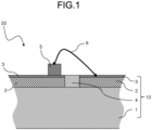
- FIG. 1 is a cross-sectional view schematically illustrating an example of peripherals of a light-emitting element in a light-emitting device of the present disclosure.
- a circuit board of the present disclosure has a high reflectance.
- the circuit board of the present disclosure is described in detail below, referring to FIG. 1 .
- a circuit board 10 of the present disclosure includes a substrate 1, a conductor layer 2 located on the substrate 1, a reflective layer 3 located on the conductor layer 2, and a resin layer 4 located on the substrate 1 to be in contact with the conductor layer 2 and the reflective layer 3.
- arithmetic mean roughness Ra obtained from a roughness profile is less than 0.2 um, and a ratio (Rku/Rsk) of kurtosis Rku obtained from the roughness profile to skewness Rsk obtained from the roughness profile is 5 or more and 15 or less.
- the surface of the reflective layer 3 refers to an exposed surface of the reflective layer 3 which reflects light.
- the arithmetic mean roughness Ra is a value defined in JIS B 0601(2013).
- the skewness Rsk is defined in JIS B 0601(2013) and is a measure of a ratio of peaks and valleys when a mean height in a roughness profile is assumed as a center line.
- the kurtosis Rku is defined in JIS B 0601(2013) and is a measure of kurtosis that is a scale of sharpness of a surface.
- the surface of the reflective layer 3 in the circuit board 10 of the present disclosure can suppress diffuse reflection of light. Further, because Rku/Rsk is 5 or more and 15 or less, the surface of the reflective layer 3 has such a surface texture that a portion around an apex of a peak becomes sharp and a ratio of valleys is large. Therefore, light can be totally reflected easily. Accordingly, the circuit board 10 of the present disclosure has a high reflectance. In the surface of the reflective layer 3 in the circuit board 10 of the present disclosure, the skewness Rsk is 1.8 or more and 2.3 or less and the kurtosis Rku is 9.0 or more and 31.9 or less, for example.
- the arithmetic mean roughness Ra, the skewness Rsk, and the kurtosis Rku in the surface of the reflective layer 3 can be obtained by performing measurement in conformity to JIS B 0601(2013). It suffices that a measurement condition is set in such a manner that a measurement length is 2.5 mm, a cut-off value is 0.08 mm, a stylus with a stylus radius of 2 ⁇ m is used, and a scan rate is 0.6 mm/s, for example. It suffices that the measurement is performed at at least three positions in the surface of the reflective layer 3 and an average value is obtained.
- a ratio (Mr2/Mr1) of a material portion Mr2 of a roughness core in a projecting valley obtained from a roughness profile to a material portion Mr1 of a roughness core in a projecting peak obtained from the roughness profile may be larger than 3.
- the material portion Mr1 of the roughness core in the projecting peak and the material portion Mr2 of the roughness core in the projecting valley are defined in JIS B 0671-2(2002) in the following manner.
- a secant line of a material ratio curve which is drawn in a center portion of the material ratio curve including 40% of measured points of a roughness profile with a difference of material portions set to 40% and which has the gentlest slope, is assumed as an equivalent line.
- a portion between two height positions of intersections of this equivalent line and the vertical axis at a material portion of 0% and at a material portion of 100% is assumed as a roughness core.
- a material portion at an intersection of the roughness profile and a separation line that separates a projecting peak above the roughness core from the roughness core is Mr1.
- a material portion at an intersection of the roughness profile and a separation line that separates a projecting valley below the roughness core from the roughness core is Mr2.
- the surface of the reflective layer 3 meets the above conditions of the configuration, a bottom of the projecting valley in that surface is wide, and therefore a regular reflectance of the reflective layer 3 becomes high, so that the circuit board 10 of the present disclosure is more excellent in a reflectance.
- the material portion Mr1 of the roughness core in the projecting peak is 24 or less and the material portion Mr2 of the roughness core in the projecting valley is 74 or more.
- a reduced valley depth Rvk obtained from the roughness profile is smaller than a reduced peak height Rpk obtained from the roughness profile.
- the reduced valley depth Rvk and the reduced peak height Rpk are defined in JIS B 0671-2(2002).
- the average depth of projecting valleys below the above-described roughness core is the reduced valley depth Rvk
- the average height of projecting peaks above the above-described roughness core is the reduced peak height Rpk.
- the surface of the reflective layer 3 meets the above conditions of the configuration, there are few projecting valleys in that surface. Therefore, a regular reflectance of the reflective layer 3 becomes high, so that the circuit board 10 of the present disclosure is further excellent in a reflectance.
- the reduced valley depth Rvk is 0.07 um or less and the reduced peak height Rpk is 0.10 um or more, for example.
- a rate of plateau whose relative material length obtained from the roughness profile is 10 to 60%, Hp(10-60%) may be 0.30 um or less, and a ratio (Hp(10-60%)/Hp(10-20%)) of the rate of plateau Hp(10-60%) to a rate of plateau whose relative material length obtained from the roughness profile is 10 to 20%, Hp(10-20%), may be less than 3.5.
- a rate of plateau Hp is defined in JIS B 0671-2(2002) in the following manner.
- the rate of plateau whose relative material length is 10 to 60%, Hp(10-60%) represents a distance between a depth at which a ratio of contact areas of a surface when the reflective layer 3 is shaved to a certain depth and a virtual plane becomes 10% and a depth at which that ratio of contact areas becomes 60%.
- the rate of plateau whose relative material length is 10 to 20%, Hp(10-20%) represents a distance between the depth at which the ratio of contact areas of the surface when the reflective layer 3 is shaved to a certain depth and the virtual plane becomes 10% and a depth at which that ratio of contact areas becomes 20%.
- the surface of the reflective layer 3 meets the above conditions of the configuration, there are few peaks and valleys in that surface. Therefore, a regular reflectance component is increased, so that a reflectance of the circuit board 10 of the present disclosure is further improved.
- the material portion Mr1 of the roughness core in the projecting peak, the material portion Mr2 in the projecting valley, the reduced valley depth Rvk, the reduced peak height Rpk, the rate of plateaus Hp in the surface of the reflective layer 3 can be obtained by performing measurement under the same measurement condition as that for the arithmetic mean roughness Ra, the skewness Rsk, and the kurtosis Rku described above, in conformity to JIS B 0671-2(2002).
- the substrate 1 in the circuit board 10 of the present disclosure is an insulator.
- the insulator include aluminum oxide ceramic, zirconium oxide ceramic, ceramic composite of aluminum oxide and zirconium oxide, silicon nitride ceramic, aluminum nitride ceramic, silicon carbide ceramic, and mullite ceramic. If the substrate 1 is made of aluminum oxide ceramic, it can be easily processed and has excellent mechanical strength. If the substrate 1 is made of aluminum nitride ceramic, it has an excellent heat dissipating property.
- aluminum oxide ceramic contains 70 mass% or more of aluminum oxide in 100 mass% of all components of ceramic.
- the material of the substrate 1 in the circuit board 10 of the present disclosure can be confirmed by the following method. First of all, measurement is performed for the substrate 1 by using an X-ray diffractometer (XRD), and identification from obtained 2 ⁇ (2 ⁇ is a diffraction angle) is performed by using a JCPDS card. Subsequently, quantitative analysis of components is performed by using an ICP atomic emission spectrophotometer (ICP) or an X-ray fluorescence spectrometer (XRF).
- ICP ICP atomic emission spectrophotometer
- XRF X-ray fluorescence spectrometer
- the material of interest is aluminum oxide ceramic. As for other ceramics, the same method can be applied.
- the conductor layer 2 in the circuit board 10 of the present disclosure may be made of any material as long as that material is conductive. If the conductor layer 2 mainly contains copper or silver, an electrical resistivity is low, and a thermal conductivity is high. Therefore, it is possible to mount a light-emitting element 5 with a large amount of heat generation on the conductor layer 2.
- the main component of the conductor layer 2 is a component whose mass% exceeds 50 mass% in 100 mass% of all components of the conductor layer 2.
- the reflective layer 3 in the circuit board 10 of the present disclosure contains at least one of gold and silver and may contain 90 mass% or more of gold and silver in total in 100 mass% of all components of the reflective layer 3.
- the reflective layer 3 in the circuit board 10 of the present disclosure may contain 95 mass% or more of gold in 100 mass% of all components of the reflective layer 3. If the reflective layer 3 contains 95 mass% or more of gold, migration hardly occurs in the reflective layer 3 when a current is caused to flow in the reflective layer 3. Therefore, the circuit board 10 of the present disclosure has excellent long-term reliability.
- the resin layer 4 in the circuit board 10 of the present disclosure has a higher reflectance than the substrate 1.
- the resin layer 4 is a resin that presents a white tone.
- the resin that presents a white tone include silicone resin, epoxy resin, or the like that contains white inorganic filler such as titanium oxide, aluminum oxide, zirconium oxide, barium oxide, barium sulfate, zinc oxide, barium titanate, or potassium titanate.
- the circuit board 10 is cut to obtain a cross-section illustrated in FIG. 1 , and the obtained cross-section is polished with a cross-section polisher (CP). Subsequently, it suffices that the polished cross-section is observed as an observation surface by using a scanning electron microscope (SEM) and the respective components of the conductor layer 2, the reflective layer 3, and the resin layer 4 are confirmed by using an energy dispersive x-ray spectrometer (EDS) attached to the SEM. Alternatively, confirmation can be performed by shaving off a portion of each of the conductor layer 2, the reflective layer 3, and the resin layer 4 and using the ICP or the XRF.
- SEM scanning electron microscope
- EDS energy dispersive x-ray spectrometer
- the substrate 1 in the circuit board 10 of the present disclosure may have a through hole. If an electrode made of a conductive material is provided in the through hole of the substrate 1, it is possible to connect the electrode to an external power supply or the like and enable electricity to be supplied. If a thermal via made of a high thermal conductivity material is provided in the through hole of the substrate 1, the heat dissipating property of the substrate 1 can be improved.
- a light-emitting device 20 of the present disclosure includes the circuit board 10 having the above-described configuration and the light-emitting element 5 located on the circuit board 10.
- FIG. 1 illustrates an example in which the light-emitting element 5 is located on a reflective layer 3 and the light-emitting element 5 is electrically connected to a reflective layer 3 by a bonding wire 6.
- a surface of the light-emitting device 20 on a side where the light-emitting element 5 is mounted, which includes the light-emitting element 5, may be covered with a sealing material or the like to protect the light-emitting element 5, although not illustrated.
- the sealing material may contain a fluorescent material and the like for wavelength conversion.
- a substrate of aluminum nitride ceramic or aluminum oxide ceramic is prepared as the substrate 1 by a known molding method and a known sintering method.
- aluminum oxide ceramic is formed, at least one of barium oxide (BaO) and zirconium oxide (ZrO 2 ) may be contained to improve a reflectance of the substrate 1.
- the through hole is formed together with an outer shape when a molded body is formed, or is formed by punching, blasting, or using laser in a molded body in which only its outer shape has been processed, or is formed in a sintered body by blasting or using laser.
- the thickness of the substrate 1 is 0.15 mm or more and 1.5 mm or less, for example.
- the average thickness of the titanium layer is 0.03 ⁇ m or more and 0.2 ⁇ m or less and the average thickness of the copper layer is 0.5 ⁇ m or more and 2 um or less, for example.
- a resist pattern is formed on the thin film by photolithography, and a new copper layer is formed by electrolytic copper plating.
- the conductor layer 2 is obtained.
- the average thickness of the copper layer formed by electrolytic copper plating is 40 ⁇ m or more and 100 ⁇ m or less, for example. Further, buffing or chemical polishing may be performed for a surface of the conductor layer 2.
- the reflective layer 3 of silver is obtained on the conductor layer 2 by performing electrolytic nickel-silver plating and/or electroless silver plating.
- the reflective layer 3 of gold is obtained on the conductor layer 2 by performing electroless nickel plating and thereafter performing electroless gold plating.
- the reflective layer 3 of gold is obtained on the conductor layer 2 by performing electroless nickel plating, electroless palladium plating, and electroless gold plating in this order.
- the reflective layer 3 In a case where a nickel layer is arranged between the conductor layer 2 and the reflective layer 3, the reflective layer 3 easily becomes glossy, so that a reflectance can be increased.
- the average thickness of the nickel layer is 1 ⁇ m or more and 10 um or less, for example.
- the average thickness of a palladium layer is 0.05 ⁇ m or more and 0.5 ⁇ m or less, for example.
- the average thickness of the reflective layer 3 is 0.1 ⁇ m or more and 10 ⁇ m or less, for example.
- the reflective layer 3 with an average thickness of 0.2 ⁇ m or more has a particularly high reflectance.
- the resist pattern is removed, and protruding portions of the thin layers of titanium and copper are removed by etching.
- the paste for resin layer is a paste in which a silicone resin material and white inorganic filler powder are dispersed in an organic solvent, for example.
- organo polysiloxane organohydrogen polysiloxane, platinum-containing polysiloxane, and the like can be used.
- white inorganic filler titanium oxide, aluminum oxide, zirconium oxide, barium oxide, barium sulfate, zinc oxide, barium titanate, potassium titanate, and the like can be used.
- organic solvent one selected from carbitol, carbitol acetate, terpineol, metacresol, dimethylimidazole, dimethyl imidazolidinone, dimethylformamide, diacetone alcohol, triethylene glycol, paraxylene, ethyl lactate, and isophorone or two or more that are selected from those materials and are mixed with each other can be used.
- a mass ratio in the paste for resin layer materials are mixed in such a manner that a mass ratio of the white inorganic filler is 0.5 to 4 and a mass ratio of the organic solvent is 20 to 100 with respect to the silicone resin material whose mass ratio is assumed as 1, for example.
- the paste for resin layer is then printed to be in contact with the conductor layer 2 and the reflective layer 3 on the substrate 1.
- the thickness of the paste for resin layer is set to be approximately equal to a total thickness of the conductor layer 2 and the reflective layer 3.
- the substrate 1 is subjected to heat treatment by being held at a maximum temperature of 140°C or more and 200°C or less for 0.5 hours or more and 3 hours or less.
- buffing is performed for surfaces of the reflective layer 3 and the resin layer 4.
- a buffing condition it suffices that abrasive grain of silicon carbide, white alumina, or diamond having a grit size of 400 or more and 3000 or less is used, and a feed rate is set to 500 mm/s or more and 2000 mm/s or less.
- chemical polishing may be additionally performed after buffing.
- a condition of chemical polishing it suffices that hydrogen peroxide solution with sulfuric acid added thereto is heated to a temperature of 50°C or more and 65°C or less, and the substrate 1 is immersed in this solution for 15 minutes or more and 45 minutes or less.
- the light-emitting device 20 of the present disclosure can be obtained by mounting the light-emitting element 5 on the reflective layer 3 of the circuit board 10 of the present disclosure, for example.
- Samples were manufactured which were different in arithmetic mean roughness Ra, skewness Rsk, and kurtosis Rku in a surface of a reflective layer, and were subjected to reflectance measurement.
- Thin layers of titanium and copper were then formed on the substrate by sputtering.
- the titanium layer and the copper layer were formed to have average thicknesses of 0.1 ⁇ m and 1.0 ⁇ m, respectively.
- a resist pattern was formed on a thin film by photolithography, and a copper layer with an average thickness of 60 um was formed by electrolytic copper plating. In this manner, a conductor layer was obtained.
- a nickel layer between the conductor layer and the reflective layer was formed to have an average thickness of 5 um, and the reflective layer was formed to have an average thickness of 3 ⁇ m.
- a paste was prepared as a paste for resin layer, in which polysiloxane as a silicone resin material and titanium oxide as white inorganic filler powder were dispersed in an organic solvent.
- the paste for resin layer was then printed to be in contact with the conductor layer and the reflective layer on the substrate. Thereafter, the substrate was subjected to heat treatment by being held at a maximum temperature of 150°C for one hour.
- the arithmetic mean roughness Ra, the skewness Rsk, and the kurtosis Rku in the surface of the reflective layer were measured by using a contact-type surface roughness measuring device in conformity to JIS B 0601(2013).
- a measurement condition a measurement length was set to 2.5 mm, a cut-off value was set to 0.08 mm, a stylus with a stylus radius of 2 ⁇ m was used, and a scan rate was set to 0.6 mm/s. The measurement was performed at three positions in the surface of the reflective layer and an average value was obtained.
- a spectrophotometer Minolta, CM-3700A
- a wavelength range was 360 to 740 nm
- a field was 10°
- an illumination diameter was 3 ⁇ 5 mm, so that a reflectance at 500 nm was measured from the measurement result.
- the reflectance of each of Samples Nos. 3 to 7 was 90.2% or more, which was higher than that of each of Samples Nos. 1, 2, and 8. It is found from this result that a surface of a reflective layer has a high reflectance when the arithmetic mean roughness Ra is smaller than 0.2 ⁇ m and a ratio of the kurtosis Rku to the skewness Rsk is 5 or more and 15 or less.
- samples were manufactured which were different in a material portion Mr1 of a roughness core in a projecting peak and a material portion Mr2 of a roughness core in a projecting valley in a surface of a reflective layer, and were subjected to reflectance measurement.
- each sample was identical to the method of manufacturing Sample No. 4 in Example 1 except that buffing and chemical polishing were performed to make a surface texture of the surface of the reflective layer have values in Table 2.
- Sample No. 9 is the same as Sample No. 4 in Example 1.
- the material portion Mr1 of the roughness core in the projecting peak and the material portion Mr2 of the roughness core in the projecting valley in the surface of the reflective layer were then measured for each of the obtained samples.
- the measurement condition was identical to that in Example 1 based on JIS B 0671-2(2002).
- a reflectance of each sample was also evaluated by the same method as that in Example 1.
- samples were manufactured which were different in a magnitude relation between a reduced valley depth Rvk and a reduced peak height Rpk in a surface of a reflective layer, and were subjected to reflectance measurement.
- each sample was identical to the method of manufacturing Sample No. 4 in Example 1 except that buffing and chemical polishing were performed to make a surface texture of the surface of the reflective layer have values in Table 3.
- Sample No. 15 is the same as Sample No. 4 in Example 1.
- the reduced valley depth Rvk and the reduced peak height Rpk in the surface of the reflective layer were measured.
- the measurement condition was identical to that in Example 1 based on JIS B 0671-2(2002).
- a reflectance of each sample was also evaluated by the same method as that in Example 1.
- each sample was identical to the method of manufacturing Sample No. 4 in Example 1 except that buffing and chemical polishing were performed to make a surface texture of the surface of the reflective layer have values in Table 4.
- Sample No. 16 is the same as Sample No. 4 in Example 1.
- the rate of plateau HP(10-60%) and the rate of plateau Hp(10-20%) in the surface of the reflective layer were measured.
- the measurement condition was identical to that in Example 1 based on JIS B 0671-2(2002).
- a reflectance of each sample was also evaluated by the same method as that in Example 1.
- Results are represented in Table 4.
- Table 4 Sample No. Hp (10-60%) ( ⁇ m) Hp (10-20%) ( ⁇ m) Hp (10-60%) /Hp(10-20%) Reflectance (%) 16 0.36 0.07 5.14 92.1 17 0.32 0.07 4.57 92.5 18 0.30 0.09 3.33 93.5 19 0.25 0.09 2.78 93.7 20 0.18 0.09 2.00 93.9 21 0.18 1.00 0.18 93.9
- samples were manufactured which were different in a component of a reflective layer, and were subjected to reflectance measurement and a migration test.
- titanium film thin layers of titanium and copper (hereinafter, simply “thin film”) were formed on the substrate by sputtering.
- the titanium layer and the copper layer were formed to have average thicknesses of 0.1 ⁇ m and 1.0 ⁇ m, respectively.
- a resist pattern was formed on the thin film by photolithography, and a copper layer with an average thickness of 60 ⁇ m was formed by electrolytic copper plating. In this manner, a conductor layer was obtained.
- the resist pattern was set in such a manner that the number of conductor layers was two after the resist pattern was removed. Specifically, the resist pattern was set in such a manner that the two conductor layers were arranged to face to such a direction that longer directions thereof were aligned with each other, and an interval between the conductor layers was 80 um.
- Each of the two conductor layers was formed to be a rectangle having a size of 400 ⁇ m ⁇ 250 um as the size of the longer direction ⁇ the shorter direction.
- electrolytic nickel-silver plating was performed to obtain a silver reflective layer on the two conductor layers.
- a nickel layer between the conductor layer and the reflective layer was formed to have an average thickness of 5 ⁇ m, and the reflective layer was formed to have an average thickness of 3 ⁇ m.
- a paste was prepared as a paste for resin layer, in which polysiloxane as a silicone resin material and titanium oxide as white inorganic filler powder were dispersed in an organic solvent.
- the paste for resin layer was printed on the substrate in the form of a square having a size of 800 ⁇ m ⁇ 800 um as the size of the longer direction ⁇ the shorter direction, to embed a gap between the two stacks and cover the stacks. Thereafter, the substrate was subjected to heat treatment by being held at a maximum temperature of 150°C for one hour.
- each sample was cut, and a cut cross-section was polished with a CP. Subsequently, the polished cross-section was observed as an observation surface by using a SEM and the components of the reflective layer were confirmed by using an EDS attached to the SEM.
- the reflective layer in Sample No. 22 contained 95 mass% or more of silver in 100 mass% of all components of the reflective layer. Meanwhile, the reflective layer in Sample No. 23 contained 95 mass% or more of gold in 100 mass% of all components of the reflective layer.
- a migration test was performed for each sample. First of all, two reflective layers in each sample were connected to each other by a conducting wire. Subsequently, each sample was placed in an environment of a high temperature (85°C) and a high humidity (85%), and was left in a state where a current was caused to flow in the reflective layers in the sample. Each sample was then taken out from the above environment every 50 hours after a current started to flow, the conducting wire connecting the two reflective layers was detached, and it was checked if the two reflective layers were electrically conducting.
- a high temperature 85°C
- 85% high humidity
- Evaluation was then performed in such a manner that an evaluation result was represented by a cross when it was confirmed that the two reflective layers were electrically conducting before 250 hours passed after a current started to flow, an evaluation result was represented by a triangle when it was confirmed that the two reflective layers were electrically conducting before 1000 hours passed after a current started to flow, and an evaluation result was represented by a circle when it was not confirmed that the two reflective layers were electrically conducting before 1000 hours passed after a current started to flow.
Landscapes
- Engineering & Computer Science (AREA)
- Microelectronics & Electronic Packaging (AREA)
- Manufacturing & Machinery (AREA)
- Computer Hardware Design (AREA)
- Power Engineering (AREA)
- Chemical & Material Sciences (AREA)
- Ceramic Engineering (AREA)
- Inorganic Chemistry (AREA)
- Led Device Packages (AREA)
- Structure Of Printed Boards (AREA)
Applications Claiming Priority (2)
| Application Number | Priority Date | Filing Date | Title |
|---|---|---|---|
| JP2017088504 | 2017-04-27 | ||
| PCT/JP2018/016330 WO2018198982A1 (ja) | 2017-04-27 | 2018-04-20 | 回路基板およびこれを備える発光装置 |
Publications (3)
| Publication Number | Publication Date |
|---|---|
| EP3618129A1 EP3618129A1 (en) | 2020-03-04 |
| EP3618129A4 EP3618129A4 (en) | 2021-01-13 |
| EP3618129B1 true EP3618129B1 (en) | 2023-03-29 |
Family
ID=63918204
Family Applications (1)
| Application Number | Title | Priority Date | Filing Date |
|---|---|---|---|
| EP18791223.3A Active EP3618129B1 (en) | 2017-04-27 | 2018-04-20 | Circuit board and light-emitting device provided with same |
Country Status (5)
| Country | Link |
|---|---|
| US (1) | US10950768B2 (zh) |
| EP (1) | EP3618129B1 (zh) |
| JP (1) | JPWO2018198982A1 (zh) |
| CN (1) | CN110603654B (zh) |
| WO (1) | WO2018198982A1 (zh) |
Families Citing this family (1)
| Publication number | Priority date | Publication date | Assignee | Title |
|---|---|---|---|---|
| JP6903210B2 (ja) * | 2019-10-15 | 2021-07-14 | Dowaエレクトロニクス株式会社 | 半導体発光素子及びその製造方法 |
Family Cites Families (18)
| Publication number | Priority date | Publication date | Assignee | Title |
|---|---|---|---|---|
| CN101410994B (zh) | 2006-03-29 | 2011-06-15 | 京瓷株式会社 | 发光装置 |
| CN101361026B (zh) * | 2006-09-27 | 2013-07-24 | 凸版印刷株式会社 | 光学元件、带标签物品、光学配套元件及判断方法 |
| JP2009129801A (ja) | 2007-11-27 | 2009-06-11 | Denki Kagaku Kogyo Kk | 金属ベース回路基板 |
| CN102257647B (zh) * | 2008-12-19 | 2014-07-23 | 古河电气工业株式会社 | 光半导体装置用引线框及其制造方法 |
| KR101718575B1 (ko) * | 2010-06-15 | 2017-03-21 | 후루카와 덴키 고교 가부시키가이샤 | 광반도체 장치용 리드 프레임, 광반도체 장치용 리드 프레임의 제조방법, 및 광반도체 장치 |
| JP2012124310A (ja) * | 2010-12-08 | 2012-06-28 | Nitto Denko Corp | 反射膜およびその製造方法 |
| JP2012151191A (ja) | 2011-01-17 | 2012-08-09 | Ibiden Co Ltd | Led用配線基板、発光モジュール、led用配線基板の製造方法、及び発光モジュールの製造方法 |
| US8846421B2 (en) * | 2011-03-10 | 2014-09-30 | Mds Co. Ltd. | Method of manufacturing lead frame for light-emitting device package and light-emitting device package |
| TW201327909A (zh) * | 2011-11-11 | 2013-07-01 | Neomax Materials Co Ltd | 發光元件用基板,發光模組及發光模組之製造方法 |
| JP5881501B2 (ja) * | 2012-03-29 | 2016-03-09 | 株式会社Neomaxマテリアル | 発光素子用基板および発光モジュール |
| JP5481577B1 (ja) * | 2012-09-11 | 2014-04-23 | Jx日鉱日石金属株式会社 | キャリア付き銅箔 |
| JP2015072754A (ja) * | 2013-10-02 | 2015-04-16 | 積水テクノ成型株式会社 | 導光板及びその製造方法 |
| JP6197696B2 (ja) | 2014-02-28 | 2017-09-20 | 日亜化学工業株式会社 | 発光装置の製造方法及び発光装置 |
| WO2015170773A1 (ja) * | 2014-05-09 | 2015-11-12 | 京セラ株式会社 | 発光素子搭載用基板および発光装置 |
| JP2016018068A (ja) * | 2014-07-08 | 2016-02-01 | 旭硝子株式会社 | 防眩膜付き基材および物品 |
| CN107113982B (zh) * | 2014-12-25 | 2020-04-10 | 住友电气工业株式会社 | 印刷配线板用基板、制作印刷配线板用基板的方法、印刷配线板、制作印刷配线板的方法以及树脂基材 |
| JP6374339B2 (ja) | 2015-03-26 | 2018-08-15 | 日亜化学工業株式会社 | 発光装置 |
| JP2017041467A (ja) * | 2015-08-17 | 2017-02-23 | ローム株式会社 | 光半導体装置 |
-
2018
- 2018-04-20 WO PCT/JP2018/016330 patent/WO2018198982A1/ja unknown
- 2018-04-20 EP EP18791223.3A patent/EP3618129B1/en active Active
- 2018-04-20 CN CN201880026881.0A patent/CN110603654B/zh active Active
- 2018-04-20 US US16/608,654 patent/US10950768B2/en active Active
- 2018-04-20 JP JP2018552888A patent/JPWO2018198982A1/ja active Pending
Also Published As
| Publication number | Publication date |
|---|---|
| JPWO2018198982A1 (ja) | 2019-06-27 |
| CN110603654B (zh) | 2023-03-21 |
| CN110603654A (zh) | 2019-12-20 |
| EP3618129A1 (en) | 2020-03-04 |
| US10950768B2 (en) | 2021-03-16 |
| US20200194640A1 (en) | 2020-06-18 |
| EP3618129A4 (en) | 2021-01-13 |
| WO2018198982A1 (ja) | 2018-11-01 |
Similar Documents
| Publication | Publication Date | Title |
|---|---|---|
| EP2387083B1 (en) | Substrate for mounting light-emitting element and light-emitting device | |
| EP2369903A1 (en) | Substrate for light-emitting element and light-emitting device | |
| EP2372798A1 (en) | Substrate for light-emitting element and light-emitting device employing it | |
| KR20110103307A (ko) | 발광 장치 | |
| JP5518168B2 (ja) | 発光素子実装用基体および発光装置 | |
| EP2413390A2 (en) | Substrate for mounting light-emitting element, production process thereof and light-emitting device | |
| EP2541629A1 (en) | Substrate for mounting light emitting element, and light emitting device | |
| JP2015120621A (ja) | ガラスセラミックス組成物、発光素子用基板、および発光装置 | |
| EP3142159B1 (en) | Substrate for mounting light-emitting element, and light-emitting device | |
| EP3618129B1 (en) | Circuit board and light-emitting device provided with same | |
| EP3355369B1 (en) | Light emitting element-mounting substrate and light emitting apparatus | |
| US20210037644A1 (en) | Circuit board and light emitting device provided with same | |
| KR20130062898A (ko) | 소자 탑재용 기판 및 그 제조 방법 | |
| CN110800118B (zh) | 电路基板以及具备该电路基板的发光装置 | |
| JP2013239546A (ja) | 発光素子搭載用基板および発光装置 | |
| JP2015070088A (ja) | 発光素子用基板および発光装置 |
Legal Events
| Date | Code | Title | Description |
|---|---|---|---|
| STAA | Information on the status of an ep patent application or granted ep patent |
Free format text: STATUS: THE INTERNATIONAL PUBLICATION HAS BEEN MADE |
|
| PUAI | Public reference made under article 153(3) epc to a published international application that has entered the european phase |
Free format text: ORIGINAL CODE: 0009012 |
|
| STAA | Information on the status of an ep patent application or granted ep patent |
Free format text: STATUS: REQUEST FOR EXAMINATION WAS MADE |
|
| 17P | Request for examination filed |
Effective date: 20191022 |
|
| AK | Designated contracting states |
Kind code of ref document: A1 Designated state(s): AL AT BE BG CH CY CZ DE DK EE ES FI FR GB GR HR HU IE IS IT LI LT LU LV MC MK MT NL NO PL PT RO RS SE SI SK SM TR |
|
| AX | Request for extension of the european patent |
Extension state: BA ME |
|
| DAV | Request for validation of the european patent (deleted) | ||
| DAX | Request for extension of the european patent (deleted) | ||
| A4 | Supplementary search report drawn up and despatched |
Effective date: 20201211 |
|
| RIC1 | Information provided on ipc code assigned before grant |
Ipc: H05K 1/03 20060101ALI20201207BHEP Ipc: H05K 3/24 20060101ALN20201207BHEP Ipc: H05K 3/28 20060101ALN20201207BHEP Ipc: H01L 33/60 20100101AFI20201207BHEP Ipc: H05K 1/18 20060101ALN20201207BHEP Ipc: H01L 33/62 20100101ALI20201207BHEP Ipc: H05K 3/16 20060101ALN20201207BHEP Ipc: H05K 3/26 20060101ALN20201207BHEP |
|
| GRAP | Despatch of communication of intention to grant a patent |
Free format text: ORIGINAL CODE: EPIDOSNIGR1 |
|
| STAA | Information on the status of an ep patent application or granted ep patent |
Free format text: STATUS: GRANT OF PATENT IS INTENDED |
|
| INTG | Intention to grant announced |
Effective date: 20221012 |
|
| GRAS | Grant fee paid |
Free format text: ORIGINAL CODE: EPIDOSNIGR3 |
|
| GRAA | (expected) grant |
Free format text: ORIGINAL CODE: 0009210 |
|
| STAA | Information on the status of an ep patent application or granted ep patent |
Free format text: STATUS: THE PATENT HAS BEEN GRANTED |
|
| AK | Designated contracting states |
Kind code of ref document: B1 Designated state(s): AL AT BE BG CH CY CZ DE DK EE ES FI FR GB GR HR HU IE IS IT LI LT LU LV MC MK MT NL NO PL PT RO RS SE SI SK SM TR |
|
| REG | Reference to a national code |
Ref country code: CH Ref legal event code: EP |
|
| REG | Reference to a national code |
Ref country code: DE Ref legal event code: R096 Ref document number: 602018047800 Country of ref document: DE |
|
| REG | Reference to a national code |
Ref country code: AT Ref legal event code: REF Ref document number: 1557269 Country of ref document: AT Kind code of ref document: T Effective date: 20230415 |
|
| REG | Reference to a national code |
Ref country code: IE Ref legal event code: FG4D |
|
| P01 | Opt-out of the competence of the unified patent court (upc) registered |
Effective date: 20230505 |
|
| REG | Reference to a national code |
Ref country code: LT Ref legal event code: MG9D |
|
| PG25 | Lapsed in a contracting state [announced via postgrant information from national office to epo] |
Ref country code: RS Free format text: LAPSE BECAUSE OF FAILURE TO SUBMIT A TRANSLATION OF THE DESCRIPTION OR TO PAY THE FEE WITHIN THE PRESCRIBED TIME-LIMIT Effective date: 20230329 Ref country code: NO Free format text: LAPSE BECAUSE OF FAILURE TO SUBMIT A TRANSLATION OF THE DESCRIPTION OR TO PAY THE FEE WITHIN THE PRESCRIBED TIME-LIMIT Effective date: 20230629 Ref country code: LV Free format text: LAPSE BECAUSE OF FAILURE TO SUBMIT A TRANSLATION OF THE DESCRIPTION OR TO PAY THE FEE WITHIN THE PRESCRIBED TIME-LIMIT Effective date: 20230329 Ref country code: LT Free format text: LAPSE BECAUSE OF FAILURE TO SUBMIT A TRANSLATION OF THE DESCRIPTION OR TO PAY THE FEE WITHIN THE PRESCRIBED TIME-LIMIT Effective date: 20230329 Ref country code: HR Free format text: LAPSE BECAUSE OF FAILURE TO SUBMIT A TRANSLATION OF THE DESCRIPTION OR TO PAY THE FEE WITHIN THE PRESCRIBED TIME-LIMIT Effective date: 20230329 |
|
| PGFP | Annual fee paid to national office [announced via postgrant information from national office to epo] |
Ref country code: DE Payment date: 20230425 Year of fee payment: 6 |
|
| REG | Reference to a national code |
Ref country code: NL Ref legal event code: MP Effective date: 20230329 |
|
| REG | Reference to a national code |
Ref country code: AT Ref legal event code: MK05 Ref document number: 1557269 Country of ref document: AT Kind code of ref document: T Effective date: 20230329 |
|
| PG25 | Lapsed in a contracting state [announced via postgrant information from national office to epo] |
Ref country code: SE Free format text: LAPSE BECAUSE OF FAILURE TO SUBMIT A TRANSLATION OF THE DESCRIPTION OR TO PAY THE FEE WITHIN THE PRESCRIBED TIME-LIMIT Effective date: 20230329 Ref country code: NL Free format text: LAPSE BECAUSE OF FAILURE TO SUBMIT A TRANSLATION OF THE DESCRIPTION OR TO PAY THE FEE WITHIN THE PRESCRIBED TIME-LIMIT Effective date: 20230329 Ref country code: GR Free format text: LAPSE BECAUSE OF FAILURE TO SUBMIT A TRANSLATION OF THE DESCRIPTION OR TO PAY THE FEE WITHIN THE PRESCRIBED TIME-LIMIT Effective date: 20230630 Ref country code: FI Free format text: LAPSE BECAUSE OF FAILURE TO SUBMIT A TRANSLATION OF THE DESCRIPTION OR TO PAY THE FEE WITHIN THE PRESCRIBED TIME-LIMIT Effective date: 20230329 |
|
| PG25 | Lapsed in a contracting state [announced via postgrant information from national office to epo] |
Ref country code: SM Free format text: LAPSE BECAUSE OF FAILURE TO SUBMIT A TRANSLATION OF THE DESCRIPTION OR TO PAY THE FEE WITHIN THE PRESCRIBED TIME-LIMIT Effective date: 20230329 Ref country code: RO Free format text: LAPSE BECAUSE OF FAILURE TO SUBMIT A TRANSLATION OF THE DESCRIPTION OR TO PAY THE FEE WITHIN THE PRESCRIBED TIME-LIMIT Effective date: 20230329 Ref country code: PT Free format text: LAPSE BECAUSE OF FAILURE TO SUBMIT A TRANSLATION OF THE DESCRIPTION OR TO PAY THE FEE WITHIN THE PRESCRIBED TIME-LIMIT Effective date: 20230731 Ref country code: ES Free format text: LAPSE BECAUSE OF FAILURE TO SUBMIT A TRANSLATION OF THE DESCRIPTION OR TO PAY THE FEE WITHIN THE PRESCRIBED TIME-LIMIT Effective date: 20230329 Ref country code: EE Free format text: LAPSE BECAUSE OF FAILURE TO SUBMIT A TRANSLATION OF THE DESCRIPTION OR TO PAY THE FEE WITHIN THE PRESCRIBED TIME-LIMIT Effective date: 20230329 Ref country code: AT Free format text: LAPSE BECAUSE OF FAILURE TO SUBMIT A TRANSLATION OF THE DESCRIPTION OR TO PAY THE FEE WITHIN THE PRESCRIBED TIME-LIMIT Effective date: 20230329 |
|
| PG25 | Lapsed in a contracting state [announced via postgrant information from national office to epo] |
Ref country code: SK Free format text: LAPSE BECAUSE OF FAILURE TO SUBMIT A TRANSLATION OF THE DESCRIPTION OR TO PAY THE FEE WITHIN THE PRESCRIBED TIME-LIMIT Effective date: 20230329 Ref country code: PL Free format text: LAPSE BECAUSE OF FAILURE TO SUBMIT A TRANSLATION OF THE DESCRIPTION OR TO PAY THE FEE WITHIN THE PRESCRIBED TIME-LIMIT Effective date: 20230329 Ref country code: IS Free format text: LAPSE BECAUSE OF FAILURE TO SUBMIT A TRANSLATION OF THE DESCRIPTION OR TO PAY THE FEE WITHIN THE PRESCRIBED TIME-LIMIT Effective date: 20230729 |
|
| REG | Reference to a national code |
Ref country code: CH Ref legal event code: PL |
|
| PG25 | Lapsed in a contracting state [announced via postgrant information from national office to epo] |
Ref country code: LU Free format text: LAPSE BECAUSE OF NON-PAYMENT OF DUE FEES Effective date: 20230420 |
|
| REG | Reference to a national code |
Ref country code: DE Ref legal event code: R097 Ref document number: 602018047800 Country of ref document: DE |
|
| REG | Reference to a national code |
Ref country code: BE Ref legal event code: MM Effective date: 20230430 |
|
| PG25 | Lapsed in a contracting state [announced via postgrant information from national office to epo] |
Ref country code: MC Free format text: LAPSE BECAUSE OF FAILURE TO SUBMIT A TRANSLATION OF THE DESCRIPTION OR TO PAY THE FEE WITHIN THE PRESCRIBED TIME-LIMIT Effective date: 20230329 |
|
| PG25 | Lapsed in a contracting state [announced via postgrant information from national office to epo] |
Ref country code: MC Free format text: LAPSE BECAUSE OF FAILURE TO SUBMIT A TRANSLATION OF THE DESCRIPTION OR TO PAY THE FEE WITHIN THE PRESCRIBED TIME-LIMIT Effective date: 20230329 Ref country code: LI Free format text: LAPSE BECAUSE OF NON-PAYMENT OF DUE FEES Effective date: 20230430 Ref country code: DK Free format text: LAPSE BECAUSE OF FAILURE TO SUBMIT A TRANSLATION OF THE DESCRIPTION OR TO PAY THE FEE WITHIN THE PRESCRIBED TIME-LIMIT Effective date: 20230329 Ref country code: CZ Free format text: LAPSE BECAUSE OF FAILURE TO SUBMIT A TRANSLATION OF THE DESCRIPTION OR TO PAY THE FEE WITHIN THE PRESCRIBED TIME-LIMIT Effective date: 20230329 Ref country code: CH Free format text: LAPSE BECAUSE OF NON-PAYMENT OF DUE FEES Effective date: 20230430 |
|
| PLBE | No opposition filed within time limit |
Free format text: ORIGINAL CODE: 0009261 |
|
| STAA | Information on the status of an ep patent application or granted ep patent |
Free format text: STATUS: NO OPPOSITION FILED WITHIN TIME LIMIT |
|
| REG | Reference to a national code |
Ref country code: IE Ref legal event code: MM4A |
|
| GBPC | Gb: european patent ceased through non-payment of renewal fee |
Effective date: 20230629 |
|
| PG25 | Lapsed in a contracting state [announced via postgrant information from national office to epo] |
Ref country code: BE Free format text: LAPSE BECAUSE OF NON-PAYMENT OF DUE FEES Effective date: 20230430 |
|
| 26N | No opposition filed |
Effective date: 20240103 |
|
| PG25 | Lapsed in a contracting state [announced via postgrant information from national office to epo] |
Ref country code: IE Free format text: LAPSE BECAUSE OF NON-PAYMENT OF DUE FEES Effective date: 20230420 |
|
| PG25 | Lapsed in a contracting state [announced via postgrant information from national office to epo] |
Ref country code: IE Free format text: LAPSE BECAUSE OF NON-PAYMENT OF DUE FEES Effective date: 20230420 Ref country code: GB Free format text: LAPSE BECAUSE OF NON-PAYMENT OF DUE FEES Effective date: 20230629 |
|
| PG25 | Lapsed in a contracting state [announced via postgrant information from national office to epo] |
Ref country code: SI Free format text: LAPSE BECAUSE OF FAILURE TO SUBMIT A TRANSLATION OF THE DESCRIPTION OR TO PAY THE FEE WITHIN THE PRESCRIBED TIME-LIMIT Effective date: 20230329 |